JAEA-Review-2010-065.pdf:15.99MB - 日本原子力研究開発機構
JAEA-Review-2010-065.pdf:15.99MB - 日本原子力研究開発機構
JAEA-Review-2010-065.pdf:15.99MB - 日本原子力研究開発機構

You also want an ePaper? Increase the reach of your titles
YUMPU automatically turns print PDFs into web optimized ePapers that Google loves.
4-06<br />
Atomistic Study of Irradiation-induced Mass<br />
Transport Process<br />
Y. Ikoma a) , T. Motooka a) , H. Sakita a) , Hafizal Yahaya a) ,<br />
H. Naramoto b) , K. Narumi b) , S. Sakai b) b, c)<br />
and Y. Maeda<br />
a) Department of Materials Science and Engineering, Kyushu University,<br />
b) Advanced Science Research Center, <strong>JAEA</strong>, c) Faculty of Engineering, Kyoto University<br />
A nanometer-sized pores (nanopores) is of great interest<br />
for a possible application to molecular sensors such as DNA<br />
sequencers 1) . These nanopores are fabricated using<br />
biomaterials and insulators. Especially, insulator<br />
nanopores are mainly fabricated by means of ion beam<br />
2, 3) 4)<br />
sculpting or electron beam exposure . We have<br />
investigated the nanopore formations utilizing the structural<br />
change in Si and by ion irradiation 5, 6) and smart cut process<br />
by hydrogen ion implantation into nanopore-formed<br />
Silicon-on-Insulator (SOI) substrates 7) .<br />
In the case of the ion irradiation technique, SOI(100)<br />
substrates with the top Si layer of 180 nm. The initial<br />
m-size holes were prepared by ~30 keV Ga + focused ion<br />
beam irradiation using HITACHI FB-2000 at Kyushu<br />
University. Then the B + , Si + , P + , and Ar + ions with the<br />
energy of 10 keV were implanted into the hole region at<br />
room temperature with doses of 4.4 × 10¹⁶ /cm 2 , 4.3 ×<br />
10 16 /cm 2 , 0.9 × 10¹⁶ /cm 2 , and 1.5 × 10¹⁶ /cm 2 , respectively.<br />
These implantations were carried out by 400 kV ion<br />
implanter at TIARA. In order to avoid possible carbon<br />
contaminations on the sample surfaces, the irradiation<br />
chamber was kept cooled by surrounding cold shrouds.<br />
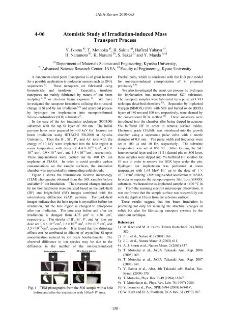
Figure 1 shows the transmission electron microscopy<br />
(TEM) photographs obtained from the SOI samples before<br />
and after P + ion irradiation. The structural changes induced<br />
by ion bombardments were analyzed based on the dark-field<br />
(DF) and bright-field (BF) images combined with the<br />
selected-area diffraction (SAD) patterns. The dark-field<br />
images indicate that the hole region is crystalline before ion<br />
irradiation, but the hole region is changed to amorphous<br />
after ion irradiation. The pore area before and after ion<br />
irradiations is changed from 4.73 m 2 to 4.56 m 2 ,<br />
respectively. The shrinks of B + , Si + , P + , and Ar + ions per<br />
dose are 0.5 × 10⁻²⁵ cm 4 , 1.8 × 10⁻²⁵ cm 4 , 1.9 × 10⁻²⁵ cm 4 , and<br />
5.5 × 10⁻²⁵ cm 4 , respectively. It is found that the shrinkage<br />
effects can be attributed to dilation of crystalline Si upon<br />
amorphization induced by ion beam bombardments. The<br />
observed difference in ion species may be due to the<br />
difference in the number of the ion-beam-induced<br />
Fig. 1 TEM photographs from the SOI sample with a hole<br />
before and after the irradiation with 10 keV P + ions.<br />
<strong>JAEA</strong>-<strong>Review</strong> <strong>2010</strong>-065<br />
- 130 -<br />
Frenkel-pairs, which is consistent with the D-D pair model<br />
for ion-beam-induced amorphization of Si proposed<br />
previously 8, 9) .<br />
We also investigated the smart cut process by hydrogen<br />
ion implantation into nanopore-formed SOI substrates.<br />
The nanopore samples were fabricated by a pulse jet CVD<br />
10)<br />
technique described elsewhere . Separation by Implanted<br />
Oxygen (SIMOX) (100) with SOI and buried oxide (BOX)<br />
layers of 180 nm and 100 nm, respectively, were cleaned by<br />
the conventional RCA method 11) . These substrates were<br />
introduced into the chamber after being dipped in aqueous<br />
5% buffered HF in order to remove surface oxides.<br />
Electronic grade CH 3SiH 3 was introduced into the growth<br />
chamber using a supersonic pulse valve with a nozzle<br />
diameter of 0.8 mm. The pulse width and frequency were<br />
set at 100 µs and 10 Hz, respectively. The substrate<br />
temperature was set at 850 °C. After forming the SiC<br />
heteroepitaxial layer and the {111} faceted pits on SOI layer,<br />
these samples were dipped into 5% buffered HF solution for<br />
10 min in order to remove the BOX layer under the pits.<br />
Hydrogen ion implantation was performed at room<br />
temperature with 1.44 MeV H 2 + up to the dose of 1 ×<br />
10 17 H/cm 2 utilizing 3 MV single-ended accelerator at TIARA.<br />
In order to separate the nanopore-grown film from SIMOX<br />
substrates, we heated the as-implanted sample at ~500 °C in<br />
air. From the scanning electron microscopy observation, it<br />
was confirmed that the sample surface was successfully cut<br />
with the depth at 10m from the substrate surface.<br />
These results suggest that ion beam irradiation is<br />
promising not only for inducing the structural changes of<br />
solids but also for fabricating nanopore systems by the<br />
smart-cut technique.<br />
References<br />
1) M. Rhee and M. A. Burns, Trends Biotechnol. 24 (2006)<br />
580.<br />
2) J. Li et al., Nature 412 (2001) 166.<br />
3) J. Li et al., Nature Mater. 2 (2003) 611.<br />
4) A. J. Storm et al., Nature Mater. 2 (2003) 537.<br />
5) T. Motooka et al., <strong>JAEA</strong> Takasaki Ann. Rep. 2006<br />
(2008) 169.<br />
6) T. Motooka et al., <strong>JAEA</strong> Takasaki Ann. Rep. 2007<br />
(2008) 140.<br />
7) Y. Ikoma et al., Abst. 4th Takasaki adv. Radiat. Res.<br />
Symp. (2009) 170.<br />
8) T. Motooka, Phys. Rev. B 49 (1994) 16367.<br />
9) T. Motooka et al., Phys. Rev. Lett. 78 (1997) 2980.<br />
10) Y. Ikoma et al., Proc. SPIE 6984 (2008) 69841V.<br />
11) W. Kern and D. A. Puotinen, RCA Rev. 31 (1970) 187.