An improved family of ZVS-PWM active-clamping DC-to ... - Ivo Barbi
An improved family of ZVS-PWM active-clamping DC-to ... - Ivo Barbi
An improved family of ZVS-PWM active-clamping DC-to ... - Ivo Barbi

You also want an ePaper? Increase the reach of your titles
YUMPU automatically turns print PDFs into web optimized ePapers that Google loves.
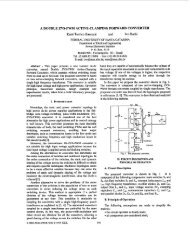
IEEE TRANSACTIONS ON POWER ELECTRONICS, VOL. 17, NO. 1, JANUARY 2002 1<br />
<strong>An</strong> Improved Family <strong>of</strong> <strong>ZVS</strong>-<strong>PWM</strong> Active-Clamping<br />
<strong>DC</strong>-<strong>to</strong>-<strong>DC</strong> Converters<br />
Cláudio Manoel C. Duarte, Member, IEEE, and <strong>Ivo</strong> <strong>Barbi</strong>, Senior Member, IEEE<br />
Abstract—A new <strong>family</strong> <strong>of</strong> dc-<strong>to</strong>-dc converters featuring<br />
<strong>clamping</strong> action, <strong>PWM</strong> modulation and s<strong>of</strong>t-switching (<strong>ZVS</strong>) in<br />
both <strong>active</strong> and passive switches, is proposed <strong>to</strong> overcome the<br />
limitations <strong>of</strong> clamped mode dc-<strong>to</strong>-dc converters. The new <strong>family</strong><br />
<strong>of</strong> converters is generated and the new circuits are presented. As<br />
the resonant circuits absorb all parasitic reactances, including<br />
transis<strong>to</strong>r output capacitance and diode junction capacitance,<br />
these converters are suitable for high-frequency operation.<br />
Principle <strong>of</strong> operation, <strong>of</strong> Boost converter, theoretical analysis,<br />
simulation and experimental results are presented, taken from<br />
a labora<strong>to</strong>ry pro<strong>to</strong>type rated at 1600 W, input voltage <strong>of</strong> 300 V,<br />
output voltage <strong>of</strong> 400 V, and operating at 100 kHz. The measured<br />
efficiency at full load was 98%.<br />
Index Terms—Active-<strong>clamping</strong>, dc-<strong>to</strong>-dc converters, s<strong>of</strong>tswitching.<br />
I. INTRODUCTION<br />
THE objective <strong>of</strong> high frequency operation in dc–dc converters<br />
is the reduction <strong>of</strong> re<strong>active</strong> components size and<br />
cost. As in any power application, high efficiency is essential,<br />
and hence the increasing <strong>of</strong> frequency can be problematic because<br />
<strong>of</strong> the direct dependence <strong>of</strong> switching losses on frequency.<br />
The use <strong>of</strong> s<strong>of</strong>t-switching techniques [1], [2], <strong>ZVS</strong> and ZCS, is<br />
an attempt <strong>to</strong> substantially reduce switching losses, and hence<br />
attain high efficiency at increased frequency.<br />
Different techniques has been proposed <strong>to</strong> operate dc-dc converters<br />
in high frequency [3]–[7]. The <strong>active</strong> <strong>clamping</strong> technique<br />
[8], [9] has the advantages <strong>of</strong> <strong>PWM</strong> modulation, s<strong>of</strong>t-commutation<br />
(<strong>ZVS</strong>) on main switches and low voltage stresses due <strong>to</strong><br />
the <strong>clamping</strong> action. Besides operating at constant frequency<br />
and with reduced commutation losses there is no significant increasing<br />
on circulating re<strong>active</strong> energy that would cause large<br />
conduction losses.<br />
The parasitic ringings caused by the interaction <strong>of</strong> the junction<br />
capacitance <strong>of</strong> the rectifier, in the clamped mode Boost converter<br />
[Fig. 1(a)], [10], and the resonant induc<strong>to</strong>r are eliminated<br />
by the inclusion <strong>of</strong> an auxiliary <strong>clamping</strong> diode [11], as shown in<br />
Fig. 1(b), limiting the voltage stress on the rectifier <strong>to</strong> the output<br />
voltage. It is important <strong>to</strong> note that <strong>to</strong> simplify the analysis, in all<br />
figures in the paper, the input filter inductance is assumed large<br />
enough <strong>to</strong> be considered as a current source and the capaci<strong>to</strong>r<br />
is selected <strong>to</strong> have a large capacitance so that the voltage<br />
Manuscript received December 22, 1999; revised July 25, 2001. Recommended<br />
by Associate Edi<strong>to</strong>r J. Qian.<br />
C. M. C. Duarte is with the Catholic University <strong>of</strong> Pelotas, Pelotas 96010-000,<br />
Brazil (e-mail: cmcd@atlas.ucpel.tche.br).<br />
I. <strong>Barbi</strong> is with the INEP, Power Electronics Institute, Federal University<br />
<strong>of</strong> Santa Catarina, Florianópolis (SC) 88040-970, Brazil (e-mail: ivo@<br />
inep.ufsc.br).<br />
Publisher Item Identifier S 0885-8993(02)02166-X.<br />
0885–8993/02$17.00 © 2002 IEEE<br />
(a) (b)<br />
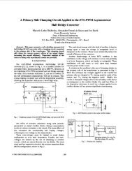
Fig. 1. Clamped mode converters: (a) without diode h and (b) with diode<br />
h .<br />
(a) (b) (c)<br />
(d) (e) (f)<br />
Fig. 2. New <strong>family</strong> <strong>of</strong> converters: (a) Buck, (b) Boost, (c) Buck-boost, (d) Cuk,<br />
(e) Sepic, and (f) Zeta.<br />
, across the capaci<strong>to</strong>r , could be considered as a constant<br />
one. Although the voltage stress on the rectifier has been eliminated,<br />
by this approach, both and diodes still present<br />
hard switching commutation and the voltages across these devices<br />
still rise in a high rate, which means compatibility<br />
electromagnetic problems and switching losses.<br />
This paper presents an <strong>improved</strong> <strong>family</strong> <strong>of</strong> dc-dc converters<br />
featuring <strong>clamping</strong> action, <strong>PWM</strong> modulation and s<strong>of</strong>t-switching<br />
(<strong>ZVS</strong>) in both <strong>active</strong> and passive switches. The inclusion <strong>of</strong><br />
capaci<strong>to</strong>r and <strong>clamping</strong> diode , in the Boost converter,<br />
as shown in Fig. 2(b), results in reduced voltage and<br />
s<strong>of</strong>t-switching conditions for all switching devices, including<br />
diodes and . Therefore all parasitic reactances are absorbed,<br />
including transis<strong>to</strong>r output capacitance and diode junction<br />
capacitance, resulting in high efficiency at high frequency<br />
operation without significant increasing in voltage and current<br />
stresses on switches.<br />
All basic dc-<strong>to</strong>-dc converters (Buck, Boost, Buck-boost, Cuk,<br />
Sepic, and Zeta) are generated from the same commutation cell
2 IEEE TRANSACTIONS ON POWER ELECTRONICS, VOL. 17, NO. 1, JANUARY 2002<br />
(a) (b)<br />
(c) (d)<br />
(e) (f)<br />
(g) (h)<br />
Fig. 3. Topological stages <strong>of</strong> Boost converter.<br />
(one switch and one diode). Therefore, if the concept <strong>of</strong> commutation<br />
cell were applied <strong>to</strong> the proposed Boost converter,<br />
shown in Fig. 1(b) with addition <strong>of</strong> capaci<strong>to</strong>r , a new commutation<br />
cell can be found. This cell is formed by or<br />
, and , and from it basic dc-<strong>to</strong>-dc<br />
<strong>to</strong>pologies are generated, the converters shown in Fig. 2. Thus,<br />
these six converters present the same behavior, in terms <strong>of</strong> commutation,<br />
and the same transfer energy principle when compared<br />
<strong>to</strong> the basic dc-<strong>to</strong>-dc converters.<br />
II. OPERATION AND ANALYSIS OF THE BOOST CONVERTER<br />
The eight <strong>to</strong>pological stages and key waveforms <strong>of</strong> the<br />
proposed Boost converter, <strong>to</strong> one switching cycle, are shown<br />
in Figs. 3 and 4, respectively. Where represents current<br />
through .<br />
From Figs. 3 and 4 it can be seen that the two switches<br />
are switched in a complementary way and s<strong>of</strong>t-switching is<br />
achieved for all switches and diodes. The main switch is<br />
turned <strong>of</strong>f at , when the switching cycle starts.<br />
A. Stage 1 ; Resonant Stage, Fig. 3(a)<br />
Prior <strong>to</strong> , the main switch is on, the auxiliary switch<br />
is <strong>of</strong>f and the <strong>clamping</strong> diode is conducting. When is<br />
turned <strong>of</strong>f, at , the first resonant stage has started, as<br />
shown in Fig. 3(a). The capaci<strong>to</strong>r is charged in a resonant<br />
way. When reaches , the antiparallel diode <strong>of</strong><br />
starts conducting and this stage ends with voltage<br />
clamped at .<br />
Fig. 4. Theoretical waveforms <strong>of</strong> Boost converter.<br />
This stage is described by<br />
where<br />
where<br />
(1)<br />
(2)<br />
B. Stage 2 ; Linear Stage [Fig. 3(b)]<br />
In this stage, the current ramps down until reaches ,<br />
when the <strong>clamping</strong> diode becomes reversibly biased and<br />
diode starts conducting.<br />
The state equations <strong>to</strong> this stage are<br />
(3)<br />
(4)<br />
(5)<br />
(6)<br />
(7)<br />
(8)<br />
(9)<br />
(10)
DUARTE AND BARBI: IMPROVED FAMILY OF <strong>ZVS</strong>-<strong>PWM</strong> ACTIVE-CLAMPING <strong>DC</strong>-TO-<strong>DC</strong> CONVERTERS 3<br />
and<br />
where<br />
(11)<br />
(12)<br />
(13)<br />
C. Stage 3 ; Resonant Stage [Fig. 3(c)]<br />
When the <strong>clamping</strong> diode ends conducting, the current<br />
through decreases and the capaci<strong>to</strong>r is charged in a resonant<br />
way. When reaches , the diode becomes forward<br />
biased and starts conducting.<br />
The equations that describe this stage are<br />
where<br />
where<br />
(14)<br />
(15)<br />
(16)<br />
(17)<br />
(18)<br />
(19)<br />
(20)<br />
D. Stage 4 ; Linear Stage [Fig. 3(d)]<br />
The current ramps down, because is considered as a<br />
constant voltage source, until it reaches zero, when it changes<br />
its direction and rises again. When the antiparallel diode <strong>of</strong><br />
is conducting, the auxiliary switch should be switched on <strong>to</strong><br />
and<br />
achieve a loss-less turn-on. This stage ends when is turned<br />
<strong>of</strong>f at .<br />
This stage is described by<br />
and<br />
where<br />
(21)<br />
(22)<br />
(23)<br />
(24)<br />
and (25)<br />
(26)<br />
E. Stage 5 ; Resonant Stage [Fig. 3(e)]<br />
The voltage across falls, due <strong>to</strong> the resonance between<br />
and , until it reaches zero at . This stage ends when<br />
becomes null and the antiparallel diode <strong>of</strong><br />
ducting [see (27)–(31) at the bot<strong>to</strong>m <strong>of</strong> the page].<br />
begins con-<br />
F. Stage 6 ; Resonant Stage [Fig. 3(f)]<br />
In stage 6, is turned on without switching losses, in a<br />
<strong>ZVS</strong> way, because became null. The current through<br />
changes its polarity and ramps up <strong>to</strong> reaches at . Then<br />
the diode becomes reversibly biased and turns <strong>of</strong>f.<br />
The state equations are<br />
and<br />
where<br />
(32)<br />
(33)<br />
(34)<br />
(35)<br />
(36)<br />
(37)<br />
(27)<br />
(28)<br />
(29)<br />
(30)<br />
(31)
4 IEEE TRANSACTIONS ON POWER ELECTRONICS, VOL. 17, NO. 1, JANUARY 2002<br />
G. Stage 7 ; Resonant Stage [Fig. 3(g)]<br />
When diode is turned <strong>of</strong>f, capaci<strong>to</strong>r and induc<strong>to</strong>r<br />
begins resonate. The voltage across reduces <strong>to</strong> zero and current<br />
through rises. This stage ends when voltage across<br />
becomes null and the <strong>clamping</strong> diode<br />
ased<br />
becomes forward bi-<br />
and<br />
(38)<br />
(39)<br />
(40)<br />
(41)<br />
(42)<br />
(43)<br />
H. Stage 8 ; Resonant Stage [Fig. 3(h)]<br />
At , the diode is conducting and the current through<br />
is clamped at . The diode is reversibly biased<br />
and power is not transferred <strong>to</strong> the load. This stage ends when<br />
is turned <strong>of</strong>f at the end <strong>of</strong> the switching cycle:<br />
and<br />
where<br />
III. CURRENT THROUGH DIODE<br />
(44)<br />
(45)<br />
(46)<br />
(47)<br />
(48)<br />
(49)<br />
The exceeding s<strong>to</strong>rage energy in (responsible by the increasing<br />
<strong>of</strong> its current beyond ) is equal <strong>to</strong> s<strong>to</strong>rage energy<br />
in capaci<strong>to</strong>r during one operation cycle , because<br />
during stage 7, transfers its whole energy <strong>to</strong> , resulting<br />
in decreasing <strong>of</strong> input voltage from <strong>to</strong> zero and increasing <strong>of</strong><br />
from <strong>to</strong> . Therefore, we have<br />
where<br />
(50)<br />
(51)<br />
(52)<br />
Thus, from (51), it may be noted that the peak value <strong>of</strong> current<br />
through depends directly on . Therefore, as greater is<br />
greater will be this current and peak current through main<br />
switch .<br />
Fig. 5. Main simplified waveforms.<br />
IV. VOLTAGE CONVERSION RATIO AND<br />
CLAMPING RATIO<br />
VOLTAGE<br />
As we can see from the waveforms <strong>of</strong> Fig. 4 and mathematical<br />
expressions from Section II, the behavior <strong>of</strong> this new boost converter<br />
is quite different respect <strong>to</strong> boost-buck-boost converter<br />
presented in [10]. However, using suitable approximations, it is<br />
possible <strong>to</strong> derive useful relations which can greatly simplify the<br />
design procedure.<br />
Thus, considering that the duration <strong>of</strong> intervals and<br />
are very small compared <strong>to</strong> switching cycle, as can be<br />
seen from Fig. 5, we have from the current balance on<br />
By assuming and<br />
(53)<br />
(54)<br />
where represents the dead time and , and solving<br />
(53), we have<br />
where<br />
(55)<br />
(56)<br />
(57)
DUARTE AND BARBI: IMPROVED FAMILY OF <strong>ZVS</strong>-<strong>PWM</strong> ACTIVE-CLAMPING <strong>DC</strong>-TO-<strong>DC</strong> CONVERTERS 5<br />
(a) (b)<br />
Fig. 6. (a) Voltage conversion ratio; (b) Voltage <strong>clamping</strong> ratio.<br />
(58)<br />
(59)<br />
As the average current through induc<strong>to</strong>r must be null in<br />
one switching cycle, we have<br />
and, as the average voltage across is<br />
so, equating (60) with (61) gives<br />
(60)<br />
(61)<br />
(62)<br />
Note that and cannot be solved analytically and are<br />
dependent, and is the normalized load current. However,<br />
based on (55) and (62), design curves can be generated for design<br />
purposes.<br />
A set <strong>of</strong> design curves showing the relationship between<br />
voltage conversion ratio and normalized load current ,<br />
for different values <strong>of</strong> duty cycle is shown in<br />
Fig. 6(a). It can be seen that for a given value <strong>of</strong> , a larger<br />
gives a lower voltage conversion ratio. This behavior is similar<br />
<strong>to</strong> that <strong>of</strong> boost-buck-boost converter [10].<br />
In Fig. 6(b) we can see a set <strong>of</strong> design curves showing the relationship<br />
between voltage <strong>clamping</strong> ratio and normalized load<br />
current , for different values <strong>of</strong> duty cycle . It can be seen<br />
that for a given value <strong>of</strong> , a larger gives a larger voltage<br />
<strong>clamping</strong> ratio, consequently a larger . In the same way, this<br />
behavior is similar <strong>to</strong> that <strong>of</strong> boost-buck-boost converter [10].<br />
The mathematical model developed here holds while<br />
is greater then zero. Therefore, from (20), we have the following<br />
constraint:<br />
This constraint is shown in Fig. 6(a).<br />
(63)<br />
V. ZERO VOLTAGE CONDITIONS<br />
In order <strong>to</strong> achieve zero voltage turn-on for , there must<br />
be sufficient energy s<strong>to</strong>red in the resonant induc<strong>to</strong>r <strong>to</strong> completely<br />
discharge the resonant capaci<strong>to</strong>r at . Thus we have<br />
then<br />
(64)<br />
(65)<br />
Equation (65) gives another constraint on . Which means that<br />
there is a minimum value <strong>of</strong> load current in CCM where <strong>ZVS</strong><br />
turn-on for is kept, and it depends directly on .<br />
VI. EXPERIMENTAL RESULTS OF THE BOOST CONVERTER<br />
The new Boost converter was implemented, with the following<br />
specifications: output power W; input<br />
voltage V; output voltage V; switching<br />
frequency kHz. The power stage consists <strong>of</strong> the<br />
following parameters:<br />
—switches and : power MOSFET’s IRFP460;—diode<br />
: APT30D60;—diode : APT15D100k—extern resonant<br />
capaci<strong>to</strong>r pF kV—extern resonant capaci<strong>to</strong>r<br />
pF kV;—capaci<strong>to</strong>r F V;—output<br />
filter : 4 capaci<strong>to</strong>rs (100 F/250 V) in series and parallel<br />
( F);—resonant induc<strong>to</strong>r H, core<br />
(E-45/15)-Thorn<strong>to</strong>n;—input filter H, core (E-55)<br />
Thorn<strong>to</strong>n.<br />
Experimentally obtained waveforms <strong>of</strong> the switches current<br />
and drain-<strong>to</strong>-source voltages and the resonant induc<strong>to</strong>r current<br />
and voltage across the resonant capaci<strong>to</strong>r are shown in Fig. 7.<br />
The voltage across diodes and and the current through<br />
those diodes are shown in Fig. 8. These waveforms agree with<br />
those predicted theoretically, and as it can be noted from the<br />
waveforms shown in Fig. 7, the main switches ( and )<br />
present <strong>ZVS</strong> commutation with clamped voltages. From Fig. 7,
6 IEEE TRANSACTIONS ON POWER ELECTRONICS, VOL. 17, NO. 1, JANUARY 2002<br />
(a) (b)<br />
Fig. 7. (a) Drain-<strong>to</strong>-source voltage across ƒ and current through ƒ<br />
(c)<br />
and g ; (b) drain-<strong>to</strong>-source voltage across ƒ and current through ƒ ; (c) voltage across<br />
g and current through v . (voltage: 100 V/div; current: 5 A/div; time scale: 2 "s/div).<br />
(a) (b)<br />
Fig. 8. (a) Voltage across h and current through h (voltage: 100 V/div; current: 5 A/div; time scale: 2 "s/div); (b) voltage across h and current through h<br />
(voltage: 100 V/div; current: 2 A/div; time scale: 2 "s/div).<br />
Fig. 9. Output voltage with different load conditions and duty cycle.<br />
it is possible <strong>to</strong> note that the diodes present ideal commutation<br />
conditions.<br />
In Fig. 9, the output voltage as a function <strong>of</strong> output current<br />
is shown, for different duty cycles, and in Fig. 10, the voltage<br />
across <strong>clamping</strong> capaci<strong>to</strong>r for the same conditions can be noted.<br />
In Fig. 11 it is shown the efficiency measurement <strong>of</strong> the<br />
<strong>ZVS</strong>-<strong>PWM</strong> Active-Clamping Boost Converter as a function <strong>of</strong><br />
Fig. 10. Voltage across the <strong>clamping</strong> capaci<strong>to</strong>r with different load conditions<br />
and duty cycle.<br />
the output power, in comparison with the conventional<br />
Hard-switching <strong>PWM</strong> Boost converter’s efficiency, at the same<br />
input and output data, and operating at the same switching<br />
frequency (100 kHz). The experimentally obtained efficiency<br />
from the new <strong>ZVS</strong>-<strong>PWM</strong> boost converter is equal <strong>to</strong> 98%, and<br />
from the conventional Hard-switching boost converter is equal
DUARTE AND BARBI: IMPROVED FAMILY OF <strong>ZVS</strong>-<strong>PWM</strong> ACTIVE-CLAMPING <strong>DC</strong>-TO-<strong>DC</strong> CONVERTERS 7<br />
Fig. 11. Experimental efficiency curve with constant output and input voltage.<br />
Fig. 12. Duty cycle variation <strong>to</strong> keep output voltage constant with different<br />
load conditions.<br />
<strong>to</strong> 95%, for rated load. The duty cycle necessary <strong>to</strong> keep the<br />
output voltage at 400 V, is shown in Fig. 12.<br />
VII. CONCLUSION<br />
A new <strong>family</strong> <strong>of</strong> dc-<strong>to</strong>-dc converters featuring <strong>clamping</strong><br />
action, <strong>PWM</strong> modulation and s<strong>of</strong>t-switching (<strong>ZVS</strong>) in both<br />
<strong>active</strong> and passive switches, is proposed <strong>to</strong> overcome the limitations<br />
<strong>of</strong> clamped mode dc-<strong>to</strong>-dc converters. As the resonant<br />
circuits absorb all parasitic reactances, including transis<strong>to</strong>r<br />
output capacitance and diode junction capacitance, these new<br />
converters operate with favorable switching conditions in all<br />
switching devices. Therefore, these converters are suitable for<br />
high-frequency operation.<br />
REFERENCES<br />
[1] K. H. Liu and F. C. Lee, “Resonant switches—A unified approach <strong>to</strong> improve<br />
performance <strong>of</strong> switching converters,” in Proc. INTELEC, 1984,<br />
pp. 344–351.<br />
[2] , “Zero-voltage switching techniques in dc/dc converter circuits,”<br />
in Proc. PESC, 1986, pp. 58–70.<br />
[3] K. W. Liu, R. Oruganti, and F. C. Lee, “Quasiresonant converters—Topologies<br />
and characteristics,” IEEE Trans. Power Electron.,<br />
vol. PEL-2, pp. 62–71, Jan. 1987.<br />
[4] M. F. Tabisz and F. C. Lee, “Zero-voltage switching multi-resonant technique—A<br />
novel approach <strong>to</strong> improve performance <strong>of</strong> high-frequency<br />
quasiresonant converters,” in Proc. PESC, 1988, pp. 9–17.<br />
[5] I. <strong>Barbi</strong>, J. C. Bolacell, D. C. Martins, and F. B. Libano, “Buck quasiresonant<br />
converter operating at constant frequency: <strong>An</strong>alysis, design and<br />
experimentation,” IEEE Trans. Power Electron., vol. 5, pp. 276–283,<br />
July 1990.<br />
[6] G. Hua, C. S. Leu, and F. C. Lee, “Novel zero-voltage-transition <strong>PWM</strong><br />
converters,” in Proc. PESC, 1992, pp. 55–61.<br />
[7] G. Hua, X. Yang, Y. Jiang, and F. C. Lee, “Novel zero-current-transition<br />
<strong>PWM</strong> converters,” in Proc. PESC, 1993, pp. 538–544.<br />
[8] R. Watson, F. C. Lee, and G. C. Hua, “Utilization <strong>of</strong> an <strong>active</strong>-clamp<br />
circuit <strong>to</strong> achieve s<strong>of</strong>t switching in flyback converters,” in Proc. PESC,<br />
1994, pp. 909–916.<br />
[9] C. M. C. Duarte and I. <strong>Barbi</strong>, “A <strong>family</strong> <strong>of</strong> <strong>ZVS</strong>-<strong>PWM</strong> <strong>active</strong>-<strong>clamping</strong><br />
dc-<strong>to</strong>-dc converters: Synthesis, analysis, design, and experimentation,”<br />
in Proc. INTELEC, 1995, pp. 502–509.<br />
[10] , “A new <strong>family</strong> <strong>of</strong> <strong>ZVS</strong>-<strong>PWM</strong> <strong>active</strong>-<strong>clamping</strong> dc-<strong>to</strong>-dc boost converters:<br />
Synthesis, analysis, and experimentation,” in Proc. INTELEC,<br />
1996, pp. 305–312.<br />
[11] M. Jovanovic, “A technique for reducing rectifier reverse-recovery-related<br />
losses in high-voltage, high-power boost converters,” in Proc.<br />
APEC, 1997, pp. 1000–1007.<br />
Cláudio Manoel C. Duarte (M’98) was born<br />
in Pelotas, Rio Grande do Sul, Brazil, in 1960.<br />
He received the B.S. degree from the Catholic<br />
University <strong>of</strong> Pelotas, Brazil, in 1982 and the M.S.<br />
and Ph.D. degrees from the Federal University <strong>of</strong><br />
Santa Catarina, Florianópolis, Brazil, in 1993 and<br />
1997, respectively, all in electrical engineering.<br />
Since August 1983, he has been Assistant<br />
Pr<strong>of</strong>essor in the Engineering School, Catholic<br />
University <strong>of</strong> Pelotas. His research interests are<br />
in the areas <strong>of</strong> dc-dc converters and power fac<strong>to</strong>r<br />
correction. He is the Vice-Rec<strong>to</strong>r <strong>of</strong> the Catholic University <strong>of</strong> Pelotas.<br />
<strong>Ivo</strong> <strong>Barbi</strong> (SM’80) was born in Gaspar, Santa<br />
Catarina, Brazil in 1949. He received the B.S. and<br />
M.S. degrees in electrical engineering from the<br />
Federal University <strong>of</strong> Santa Catarina, Florianópolis,<br />
Brazil, in 1973 and 1976, respectively, and the Ph.D.<br />
degree from the Institute National Polytechnique de<br />
Toulouse, France, in 1979.<br />
He founded The Brazilian Power Electronics<br />
Society and the Power Electronics Institute, Federal<br />
University <strong>of</strong> Santa Catarina. Currently, he is a<br />
Pr<strong>of</strong>essor <strong>of</strong> the Power Electronics Institute.<br />
Dr. <strong>Barbi</strong> has been an Associate Edi<strong>to</strong>r <strong>of</strong> the Power Converters Section, IEEE<br />
TRANSACTIONS ON INDUSTRIAL ELECTRONICS, since January 1992.