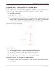
BJT Characteristic Curves
BJT Characteristic Curves
BJT Characteristic Curves

You also want an ePaper? Increase the reach of your titles
YUMPU automatically turns print PDFs into web optimized ePapers that Google loves.
Section C4: <strong>BJT</strong> <strong>Characteristic</strong> <strong>Curves</strong><br />
It is sometimes helpful to view the characteristic curves of the transistor in<br />
graphical form. This is very similar to the graphical approach used with<br />
diodes, but now we have three possible points where something could be<br />
happening (base, emitter, collector). We’re still going to concentrate on<br />
normal active mode operation here and talk about the two pn junctions in<br />
the <strong>BJT</strong> separately.<br />
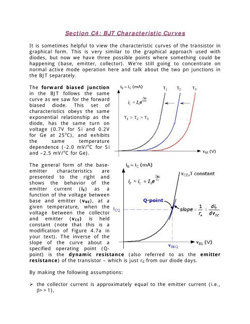
The forward biased junction<br />
in the <strong>BJT</strong> follows the same<br />
curve as we saw for the forward<br />
biased diode. This set of<br />
characteristics obeys the same<br />
exponential relationship as the<br />
diode, has the same turn on<br />
voltage (0.7V for Si and 0.2V<br />
for Ge at 25 o C), and exhibits<br />
the same temperature<br />
dependence (-2.0 mV/ o C for Si<br />
and –2.5 mV/ o C for Ge).<br />
The general form of the baseemitter<br />
characteristics are<br />
presented to the right and<br />
shows the behavior of the<br />
emitter current (iE) as a<br />
function of the voltage between<br />
base and emitter (vBE), at a<br />
given temperature, when the<br />
voltage between the collector<br />
and emitter (vCE) is held<br />
constant (note that this is a<br />
modification of Figure 4.7a in<br />
your text). The inverse of the<br />
slope of the curve about a<br />
specified operating point (Qpoint)<br />
is the dynamic resistance (also referred to as the emitter<br />
resistance) of the transistor – which is just rd from our diode days.<br />
By making the following assumptions:<br />
the collector current is approximately equal to the emitter current (i.e.,<br />
β>>1),
the nonideality factor n is equal to one, and<br />
room temperature operation;<br />
the emitter resistance may be calculated by (bear with me please, I don’t<br />
like to have massive quantities of derivations, but I had to go back and<br />
prove this to myself again so I decided to write it down):<br />
1<br />
r<br />
e<br />
=<br />
di<br />
dv<br />
E<br />
BE<br />
I<br />
=<br />
V<br />
Substituting VT=26mV at room temperature, iE (iC) at the Q-point, and<br />
solving for re (rd), we get<br />
r<br />
d<br />
0<br />
T<br />
= r<br />
e<br />
e<br />
v<br />
V<br />
BE<br />
T<br />
i<br />
=<br />
V<br />
E<br />
T<br />
.<br />
26mV<br />
=<br />
ICQ<br />
. (Equation 4.19)<br />
Note that, if the temperature changes, VT will no longer be 26mV.<br />
The actual iC-vBE characteristics behave identically to the curve above, but<br />
have a scaling factor of α (I0 in the equation above becomes αI0). However,<br />
since usually α ≈ 1, this is generally disregarded. Similarly, the iB-vBE<br />
characteristics have the same appearance, but with a scaled current of I0/β.<br />
Finally, the curves for a pnp transistor will look the same, but the polarity<br />
on the base-emitter voltage will be switched (vBE becomes –vBE=vEB).<br />
The second set of<br />
characteristics we’re going to<br />
be interested in is illustrated<br />
to the right as a family of iCvCE<br />
curves (note that this is a<br />
modified combination of<br />
Figures 4.7(b) and 4.8 of your<br />
text). Each of the curves in<br />
this family illustrates the<br />
dependence of the collector<br />
current (iC) on the collector<br />
emitter voltage (vCE) when<br />
the base current (iB) has a<br />
constant value (i.e., vBE is<br />
held constant).<br />
There are three distinct
egions of these characteristics that are of importance:<br />
As the magnitude of vCE decreases, there comes a point when the<br />
collector voltage becomes less than the base voltage. When this happens,<br />
the transistor leaves the linear region of operation and enters the<br />
saturation region, which is highly nonlinear and is not usable for<br />
amplification.<br />
The cutoff region of operation occurs for base currents near zero. In the<br />
cutoff region, the collector current approaches zero in a nonlinear manner<br />
and is also avoided for amplification applications.<br />
The linear region is where we want to be for amplification. In the linear<br />
(or active) region the curves would ideally be horizontal straight lines,<br />
indicating that the collector behaves as a constant current source<br />
independent of the collector voltage, as illustrated in the hybrid-π model<br />
(iC = βiB). Practically, these curves have a slight positive slope. If these<br />
curves are extended to the left along the –vCE axis, they will converge to<br />
a point known as the Early voltage, shown as –VA in the figure below (a<br />
modified version of Figure 4.10 in your text).<br />
The Early Voltage (note that VA > 0), is a figure of merit that is<br />
dependent on the particular transistor and defines how close to ideal the<br />
ideal behaves (for an ideal curve, the Early Voltage would be infinity).<br />
The magnitude of the Early voltage typically falls in the range of 50 –<br />
100V for practical devices.<br />
Using the value of VA, we can define the output resistance of the<br />
transistor (ro in the hybrid-π model or hoe -1 in the h-parameter model) for<br />
a specific value of collector current. Although ro is strictly defined as the<br />
inverse of the partial derivative of iC with respect to vCE at a constant<br />
value of iB (yikes!), the same result is achieved by taking the inverse of<br />
the slope of the curve and realizing that VA >> VCE:
V<br />
r o =<br />
I<br />
A<br />
C<br />
. (Equation 4.21)<br />
The characteristic curves for a transistor provide a<br />
powerful tool in the design and analysis of transistor<br />
circuits. Figure 4.9, slightly modified and presented<br />
to the right, illustrates a simple transistor circuit. By<br />
using KVL around the collector to emitter loop<br />
(remember that the other side of VCC is tied to<br />
ground), by using the approximation that iC ≈ iE, and<br />
by restricting ourselves to the dc values of circuit<br />
parameters,<br />
V CC = IC<br />
( RC<br />
+ RE<br />
) + VCE<br />
. (Equation 4.20)<br />
By defining the two extremes in this equation; i.e., when<br />
IC = 0, VCE= VCC and<br />
VCE=0, IC=VCC/(RE+RC);<br />
the endpoints of the dc load line are defined as illustrated in the figure<br />
below (Figure 4.8-ish of your text). The dc load line is determined by the<br />
resistors RC and RE in the circuit, where the quantity RE+RC has been given<br />
the designation Rdc, or dc circuit resistance, in the calculation of ICC. The<br />
intersection of the dc load line with a specific iB curve defines the quiescent<br />
point (Q-point) for circuit operation in terms of IBQ, ICQ and VCEQ. We’re just<br />
talking about dc right now, but we’ll see that the Q-point represents the dc<br />
bias, or starting point, for the transistor circuit and that the variations about<br />
this point carry the information (ac signals) in the circuit. Also, the Rdc<br />
designation will make more sense… we’ll see that under ac operation we<br />
may have a different equivalent circuit resistance that, big surprise, we’re<br />
going to call Rac!
We’ve now got enough information in terms of models and<br />
characteristics to actually do something with the <strong>BJT</strong>! In the<br />
remainder of this section of our studies, we’re going to discuss the<br />
general characteristics of single stage <strong>BJT</strong> amplifiers in terms of<br />
configurations, biasing, and power considerations. Hang on!