MEMS Accelerometers
MEMS Accelerometers
MEMS Accelerometers

You also want an ePaper? Increase the reach of your titles
YUMPU automatically turns print PDFs into web optimized ePapers that Google loves.
<strong>MEMS</strong><br />
<strong>Accelerometers</strong><br />
Constantine, Friedman & Goldberg, LLP<br />
<strong>MEMS</strong> Accelerometer
Outline<br />
Accelerometer Quick Study<br />
– Background and device market<br />
– Purpose and function<br />
– Control variables<br />
Proposed Modification<br />
– Impacting performance by process modification<br />
– Preventing failure modes<br />
Economic Model<br />
– Drivers of cost structure<br />
– Impact of proposal<br />
<strong>MEMS</strong> Accelerometer
Quick-Study: Background<br />
<strong>MEMS</strong><br />
– Micro ElectroMechanical Systems<br />
– Small devices that perform the same function as larger<br />
mechanical systems<br />
– Usually “machined” out of silicon<br />
<strong>Accelerometers</strong><br />
– Devices that are used to measure acceleration<br />
– Used for airbag sensors, etc.<br />
– <strong>MEMS</strong> version is smaller, lighter, and cheaper than<br />
traditional alternatives<br />
<strong>MEMS</strong> Accelerometer
Quick-Study: Accelerometer Market<br />
Primary Market<br />
– Automobile Airbag Sensors<br />
– Approximately 50 million sensors/year<br />
– Sensors sell for approximately $10 each<br />
Secondary Markets<br />
– Computer Joysticks<br />
– Military Applications<br />
– Amusement Park Technology<br />
<strong>MEMS</strong> Accelerometer
Quick-Study: Purpose and Function<br />
Purpose: microchip sensor to detect<br />
acceleration<br />
<strong>MEMS</strong> Accelerometer
Quick-Study: Purpose and Function<br />
Purpose: microchip sensor to detect<br />
acceleration<br />
Functional Features:<br />
<strong>MEMS</strong> Accelerometer
Quick-Study: Purpose and Function<br />
Purpose: microchip sensor to detect<br />
acceleration<br />
Functional Features:<br />
Proof Mass<br />
<strong>MEMS</strong> Accelerometer
Quick-Study: Purpose and Function<br />
Purpose: microchip sensor to detect<br />
acceleration<br />
Functional Features:<br />
Proof Mass<br />
Suspension Arms<br />
<strong>MEMS</strong> Accelerometer
Quick-Study: Purpose and Function<br />
Purpose: microchip sensor to detect<br />
acceleration<br />
Functional Features:<br />
Proof Mass<br />
Suspension Arms<br />
Substrate with Circuitry<br />
<strong>MEMS</strong> Accelerometer
Quick-Study: Purpose and Function<br />
Purpose: microchip sensor to detect<br />
acceleration<br />
Functional Features:<br />
Proof Mass<br />
Suspension Arms<br />
Substrate with Circuitry<br />
Axis of Response<br />
<strong>MEMS</strong> Accelerometer
Quick-Study: Purpose and Function<br />
Purpose: microchip sensor to detect<br />
acceleration<br />
Functional Features:<br />
Proof Mass<br />
Suspension Arms<br />
Substrate with Circuitry<br />
Axis of Response<br />
Sensing Function<br />
<strong>MEMS</strong> Accelerometer
Quick-Study: Purpose and Function<br />
Purpose: microchip sensor to detect<br />
acceleration<br />
Functional Features:<br />
Proof Mass<br />
Suspension Arms<br />
Substrate with Circuitry<br />
Axis of Response<br />
Sensing Function<br />
Piezoresistive Strain Gauge<br />
Piezo<br />
Material on<br />
Suspension<br />
Arm<br />
<strong>MEMS</strong> Accelerometer
Quick-Study: Purpose and Function<br />
Purpose: microchip sensor to detect<br />
acceleration<br />
Functional Features:<br />
Proof Mass<br />
Suspension Arms<br />
Substrate with Circuitry<br />
Axis of Response<br />
Sensing Function<br />
Capacitive<br />
Capacitance<br />
Varies with<br />
Gap Spacing<br />
<strong>MEMS</strong> Accelerometer
Quick-Study: Purpose and Function<br />
Purpose: microchip sensor to detect<br />
acceleration<br />
Functional Features:<br />
Proof Mass<br />
Suspension Arms<br />
Substrate with Circuitry<br />
Axis of Response<br />
Sensing Function<br />
Capacitive (Analog Devices)<br />
<strong>MEMS</strong> Accelerometer
Quick Study: Control Variables<br />
Dash pot, c Mass, m Spring, k<br />
Motion Limiters<br />
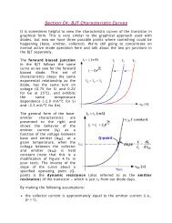
Modeled as a spring/dashpot: F = ma = kx + cx .<br />
Model gives control relationships...<br />
1. Static sensitivity:<br />
x static (s)<br />
a(s)<br />
M<br />
=<br />
K<br />
=<br />
1<br />
ω r 2<br />
ω r = (K / M) 1/2 = Natural Resonance Frequency<br />
2. Total Noise: =<br />
(4KTc)<br />
M<br />
1/2<br />
TN<br />
Increased Increased mass mass more sensitive, less noise<br />
<strong>MEMS</strong> Accelerometer
Proposed Modification: Economics<br />
Increased Increased mass mass more sensitive, less noise<br />
Increase the density<br />
Decrease the size of the proof mass<br />
Increase the number of devices per<br />
wafer<br />
Obtain greater throughput or decreased<br />
material input.<br />
<strong>MEMS</strong> Accelerometer
Techniques to Add Mass<br />
Ion Implanting of Metal<br />
CVD of Metal<br />
Sputtering of Metal<br />
<strong>MEMS</strong> Accelerometer
Ion Implanting<br />
Benefits<br />
– No masking and post-mask etching required.<br />
– Sensitive control of deposited quantities<br />
Problems<br />
– Causes high stress, therefore annealing is required.<br />
– Damages the underlying silicon crystal structure, I.e. fracture points that may<br />
remain after the anneal.<br />
– Sputter some of the surface silicon.<br />
– Most expensive equipment<br />
– Only small gains in densification<br />
(+2%) w/annealing<br />
(+0.4%) w/heavy metal doping<br />
<strong>MEMS</strong> Accelerometer
CVD of Metal<br />
Benefits<br />
– Rich history of use for metal interconnects (Al/Cu, or W)<br />
i.e. WF6(g) + 3H2(s) = W(s) + 6HF(g)<br />
– Relatively low stress application (no annealing required)<br />
– Equipment is already used by <strong>MEMS</strong> Accelerometer manufacturers<br />
(although not for metallization).<br />
Problems<br />
– HF formation causes “worm-holes.”<br />
– Impurities in metal cause “encroachment”, where Si and SiO2 layers<br />
separate.<br />
– Pure tungsten layers de-laminate at the edges.<br />
– CVD metallization is new for <strong>MEMS</strong> accelerometer manufacturers<br />
– sputtered metal film pretreatment is required for adhesion of metal.<br />
<strong>MEMS</strong> Accelerometer
Sputtering Metal<br />
The Best Choice<br />
Problems<br />
– Annealing is required after application.<br />
– High sputter rates lead to non-uniform coverage (cosine law).<br />
– Typically lower growth rate than CVD.<br />
– Plasma energy must be optimized.<br />
Benefits<br />
– Rich history of use.<br />
– This is “line-of-sight.”<br />
– Alloy concentrations can be carefully controlled.<br />
– This equipment is already used for metallization of <strong>MEMS</strong>!!<br />
– Adding W-Ti alloy is recommended<br />
<strong>MEMS</strong> Accelerometer
Best Choice<br />
Sputtering<br />
– Problems with the other technologies<br />
CVD has “worm-holes” and encroachment, and requires<br />
sputtering pretreatment.<br />
Ion Implanting causes damage and has expensive<br />
equipment.<br />
<strong>MEMS</strong> Accelerometer
The Process of Adding Mass<br />
Proof Mass<br />
=<br />
=<br />
=<br />
=<br />
Doped Silicon<br />
Photoresist<br />
Fluoropolymer<br />
Metal Layer<br />
Proof Mass<br />
Pattern Photoresist W-Ti Sputtering<br />
Proof Mass<br />
Lift-Off (acetone)<br />
Proof Mass<br />
Fluoropolymer<br />
Deposition<br />
(prevents stiction)<br />
Proof Mass<br />
<strong>MEMS</strong> Accelerometer
Modes of Failure<br />
Stiction<br />
– 2 clean Si surfaces stuck together by Van der Waals<br />
forces<br />
– prevent with fluoropolymer and motion stops<br />
Adhesion<br />
– metal layer delamination<br />
– prevent with Ti “glue” layer which creates strong<br />
W/Ti/Si bond<br />
Dirt/junk/dust in capacitive gaps<br />
– stops motion of proof mass; obscures signal<br />
– prevented with careful packaging of device<br />
<strong>MEMS</strong> Accelerometer
Economic Justification<br />
It is possible to add a<br />
layer with a density of<br />
16.6 g/cm 3 .<br />
– Assume this layer is 0.5<br />
microns thick<br />
This makes the density<br />
of the proof mass 5.2<br />
g/cm 3<br />
– (Silicon [ρ=2.3g/cm 3 ] is 2<br />
microns thick, 80% of<br />
volume, rest is metal layer)<br />
<strong>MEMS</strong> Accelerometer
Economic Justification<br />
Given that the proof mass is 1µg<br />
– And assuming Length = 2 Width, thickness = 2 micron<br />
– The original proof mass is 660 by 330 microns.<br />
With the new density and thickness<br />
– The new proof mass is 200 by 400 microns.<br />
Assuming that the device can be scaled<br />
based on the longer dimension.<br />
– This gives 15% additional devices per wafer = 9 M<br />
additional devices per year - without changing throughput!<br />
<strong>MEMS</strong> Accelerometer
Conclusion<br />
Sensitivity directly varies with mass; noise<br />
decreases with increasing mass<br />
Can make more sensitive devices of same size<br />
or smaller devices of same sensitivity<br />
Evaluation of processing options shows<br />
sputtering with W/Ti is optimal and<br />
economically viable<br />
Modes of failure preventable ensuring<br />
continued reliable devices with new process<br />
<strong>MEMS</strong> Accelerometer
QUESTIONS?<br />
<strong>MEMS</strong> Accelerometer