2011 - Cooperative Institute for Research in Environmental Sciences ...
2011 - Cooperative Institute for Research in Environmental Sciences ...
2011 - Cooperative Institute for Research in Environmental Sciences ...

Create successful ePaper yourself
Turn your PDF publications into a flip-book with our unique Google optimized e-Paper software.
Lang Farmer<br />
Development of a Micro<strong>in</strong>terdigitated<br />
Electrode Array <strong>for</strong> Use <strong>in</strong> High-Precision<br />
TIMS-Based Isotope Ratio Determ<strong>in</strong>ations<br />
FUNDING: NATIONAL SCIENCE FOUNDATION<br />
34 CIRES Annual Report <strong>2011</strong><br />
Thermal ionization<br />
mass spectrometry (TIMS)<br />
rema<strong>in</strong>s the method of<br />
choice <strong>for</strong> high-precision<br />
lead (Pb) isotopic measurements,<br />
but “silica gel”<br />
techniques used to generate<br />
thermalized Pb ions<br />
have ionization efficiencies<br />
of only 10 percent at best.<br />
To improve Pb ionization<br />
efficiencies from liquid<br />
glass ion emitters and,<br />
ultimately, the precision of<br />
uranium-Pb age determ<strong>in</strong>ations,<br />
we are us<strong>in</strong>g<br />
electrochemical techniques<br />
to <strong>in</strong>crease Pb ionization<br />
efficiencies <strong>in</strong> situ <strong>in</strong> liquid<br />
glasses. Our <strong>in</strong>itial work demonstrated that Pb-doped hightemperature<br />
(about 1,300°C) liquid glass can serve as the<br />
electrolyte <strong>in</strong> an electrochemical cell and that Pb metal atoms<br />
prevalent <strong>in</strong> the glass under vacuum conditions can be oxidized<br />
to Pb+ by the application of about 1 V across plat<strong>in</strong>um<br />
wire electrodes.<br />
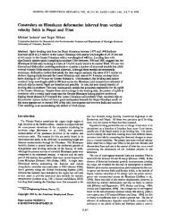
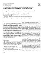
To take advantage of this ionization mechanism, we are<br />
develop<strong>in</strong>g a micro-<strong>in</strong>terdigitated electrode array (IDA) <strong>for</strong><br />
use as an “electrochemical” ion source. This array consists<br />
of a “comb” structure of <strong>in</strong>terleaved tungsten electrode “f<strong>in</strong>gers”<br />
sputtered onto a pure silicon wafer. The array fabrication<br />
process <strong>in</strong>cludes sp<strong>in</strong>n<strong>in</strong>g photoresist on an oxidized 275<br />
μm-thick silicon wafer and expos<strong>in</strong>g the wafer to ultraviolet<br />
light through a photomask. The DC (direct current) sputter<br />
deposition system applies a 1-μm layer of tungsten to the<br />
wafer. A photoresist liftoff procedure removes most of the<br />
metal layer, leav<strong>in</strong>g the IDA structures on the wafer. The electrode<br />
lengths and widths range from 100–200 μm and 10–200<br />
μm, respectively. There are one to 14 pairs of these electrodes<br />
on each IDA, with gap widths of 10–15 μm. Our <strong>in</strong>itial results<br />
reveal that a Pb-doped silica suspension can be dried and<br />
melted on the IDA surface by a metal ribbon resistive heater<br />
placed <strong>in</strong> contact with the electrically nonconduct<strong>in</strong>g silicon<br />
wafer substrate of the IDA. Our next step will be to <strong>in</strong>stall<br />
the IDA and heater ribbon <strong>in</strong> a F<strong>in</strong>nigan-MAT 261 TIMS, and<br />
to connect the assembly to a specially designed potentiostat<br />
that will allow the IDA to float at 10 kV while a differential<br />
voltage from 0.1 to 10 V is applied across the IDA electrodes.<br />
This work is currently <strong>in</strong> progress.<br />
Silica wafer with several different micro-<strong>in</strong>terdigitated<br />
electrode arrays, each <strong>for</strong>med from tungsten layers<br />
sputtered onto the wafer surface.