- Page 1 and 2:
Xilinx Synthesis Technology (XST) U
- Page 3 and 4:
About This Manual Manual Contents T
- Page 5 and 6:
Resource Description/URL About This
- Page 7 and 8:
Conventions Typographical This manu
- Page 9 and 10:
Contents About This Manual Conventi
- Page 11 and 12:
Contents 8-bit Shift-Left Register
- Page 13 and 14:
Contents Dividers .................
- Page 15 and 16:
Contents Verilog Flow: ............
- Page 17 and 18:
Contents Sequential Process with a
- Page 19 and 20:
Introduction Architecture Support X
- Page 21 and 22:
Introduction 4. Set the desired Syn
- Page 23 and 24:
Figure 1-1 View Synthesis Report In
- Page 25 and 26:
HDL Coding Techniques This chapter
- Page 27 and 28:
HDL Coding Techniques The following
- Page 29 and 30:
HDL Coding Techniques The following
- Page 31 and 32:
Table 2-1 VHDL and Verilog Examples
- Page 33 and 34:
Table 2-1 VHDL and Verilog Examples
- Page 35 and 36:
Table 2-1 VHDL and Verilog Examples
- Page 37 and 38:
Signed/Unsigned Support Registers H
- Page 39 and 40:
Flip-flop with Positive-Edge Clock
- Page 41 and 42:
HDL Coding Techniques The following
- Page 43 and 44:
VHDL Code HDL Coding Techniques Fol
- Page 45 and 46:
HDL Coding Techniques The following
- Page 47 and 48:
IO Pins Description CE Clock Enable
- Page 49 and 50:
Log File HDL Coding Techniques The
- Page 51 and 52:
HDL Coding Techniques Verilog Code
- Page 53 and 54:
HDL Coding Techniques 4-bit Latch w
- Page 55 and 56:
Tristates Log File HDL Coding Techn
- Page 57 and 58:
VHDL Code HDL Coding Techniques Fol
- Page 59 and 60:
Counters HDL Coding Techniques XST
- Page 61 and 62:
VHDL Code HDL Coding Techniques Fol
- Page 63 and 64:
HDL Coding Techniques 4-bit Unsigne
- Page 65 and 66:
HDL Coding Techniques entity counte
- Page 67 and 68:
Verilog Code HDL Coding Techniques
- Page 69 and 70:
HDL Coding Techniques 4-bit Unsigne
- Page 71 and 72:
VHDL Code HDL Coding Techniques Fol
- Page 73 and 74:
Accumulators HDL Coding Techniques
- Page 75 and 76:
VHDL Code HDL Coding Techniques Fol
- Page 77 and 78:
HDL Coding Techniques • shift mod
- Page 79 and 80:
Log File HDL Coding Techniques The
- Page 81 and 82:
Verilog Code HDL Coding Techniques
- Page 83 and 84:
HDL Coding Techniques 8-bit Shift-L
- Page 85 and 86:
VHDL Code HDL Coding Techniques Fol
- Page 87 and 88:
VHDL Code HDL Coding Techniques Fol
- Page 89 and 90:
Verilog Code HDL Coding Techniques
- Page 91 and 92:
Verilog Code HDL Coding Techniques
- Page 93 and 94:
Dynamic Shift Register module shift
- Page 95 and 96:
library IEEE; use IEEE.std_logic_11
- Page 97 and 98:
HDL Coding Techniques The following
- Page 99 and 100:
neither Full nor Parallel module no
- Page 101 and 102:
Related Constraints Related constra
- Page 103 and 104:
HDL Coding Techniques entity mux is
- Page 105 and 106:
Verilog Code HDL Coding Techniques
- Page 107 and 108:
Decoders Log File HDL Coding Techni
- Page 109 and 110:
VHDL (One-Cold) Following is the VH
- Page 111 and 112:
VHDL Following is the VHDL code. li
- Page 113 and 114:
VHDL Following is the VHDL code. li
- Page 115 and 116:
Priority Encoders Log File HDL Codi
- Page 117 and 118:
Verilog Logical Shifters HDL Coding
- Page 119 and 120:
Example 1 HDL Coding Techniques The
- Page 121 and 122:
VHDL Following is the VHDL code. li
- Page 123 and 124:
Verilog Arithmetic Operations Follo
- Page 125 and 126: Unsigned 8-bit Adder HDL Coding Tec
- Page 127 and 128: HDL Coding Techniques Verilog Follo
- Page 129 and 130: HDL Coding Techniques Verilog Follo
- Page 131 and 132: Simple Signed 8-bit Adder HDL Codin
- Page 133 and 134: Unsigned 8-bit Adder/Subtractor HDL
- Page 135 and 136: Comparators (=, /=,=) HDL Coding Te
- Page 137 and 138: HDL Coding Techniques this, XST can
- Page 139 and 140: Dividers HDL Coding Techniques VHDL
- Page 141 and 142: HDL Coding Techniques Verilog Follo
- Page 143 and 144: B C A OPER +/- RES OPER X8984 HDL C
- Page 145 and 146: HDL Coding Techniques • RAM descr
- Page 147 and 148: HDL Coding Techniques entity raminf
- Page 149 and 150: HDL Coding Techniques VHDL The foll
- Page 151 and 152: HDL Coding Techniques Verilog The f
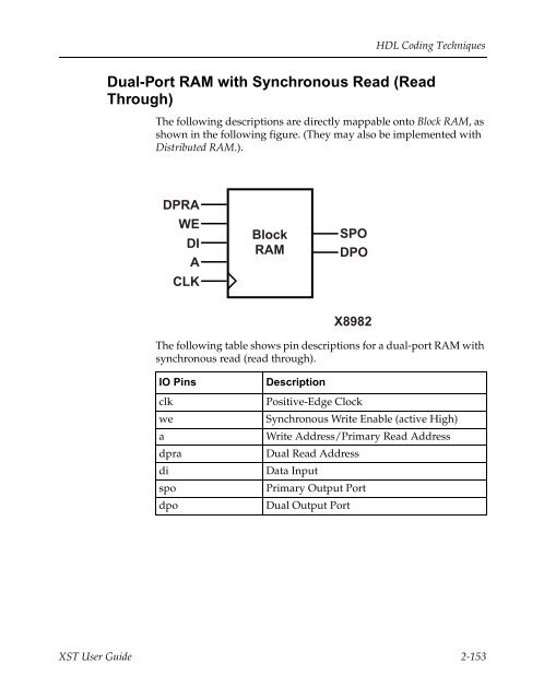
- Page 153 and 154: HDL Coding Techniques VHDL The foll
- Page 155 and 156: Log File HDL Coding Techniques The
- Page 157 and 158: VHDL Following is the VHDL code for
- Page 159 and 160: HDL Coding Techniques Single-Port R
- Page 161 and 162: Verilog HDL Coding Techniques Follo
- Page 163 and 164: VHDL Following is the VHDL code. li
- Page 165 and 166: HDL Coding Techniques Single-Port R
- Page 167 and 168: Verilog Following is the Verilog co
- Page 169 and 170: VHDL HDL Coding Techniques Followin
- Page 171 and 172: Dual-Port RAM with Asynchronous Rea
- Page 173 and 174: Verilog Following is the Verilog co
- Page 175: VHDL HDL Coding Techniques Followin
- Page 179 and 180: Verilog HDL Coding Techniques Follo
- Page 181 and 182: HDL Coding Techniques architecture
- Page 183 and 184: HDL Coding Techniques Dual-Port RAM
- Page 185 and 186: Verilog HDL Coding Techniques Follo
- Page 187 and 188: VHDL HDL Coding Techniques Followin
- Page 189 and 190: Verilog HDL Coding Techniques Follo
- Page 191 and 192: VHDL HDL Coding Techniques Followin
- Page 193 and 194: Verilog Following is the Verilog co
- Page 195 and 196: VHDL Following is the VHDL code for
- Page 197 and 198: Inputs Next State Function RESET CL
- Page 199 and 200: FSM with 1 Process HDL Coding Techn
- Page 201 and 202: Inputs FSM with 2 Processes HDL Cod
- Page 203 and 204: Verilog HDL Coding Techniques Follo
- Page 205 and 206: process2 : process (state, x1) begi
- Page 207 and 208: State Registers HDL Coding Techniqu
- Page 209 and 210: Compact HDL Coding Techniques Compa
- Page 211 and 212: Black Box Support Log File HDL Codi
- Page 213 and 214: Verilog Following is the Verilog co
- Page 215 and 216: FPGA Optimization Introduction This
- Page 217 and 218: Macro Generation • Number of Cloc
- Page 219 and 220: Multiplexers FPGA Optimization For
- Page 221 and 222: RAMs FPGA Optimization Two types of
- Page 223 and 224: Flip-Flop Retiming FPGA Optimizatio
- Page 225 and 226: FPGA Optimization INCREMENTAL_SYNTH
- Page 227 and 228:
FPGA Optimization Note In the curre
- Page 229 and 230:
FPGA Optimization generated NGC fil
- Page 231 and 232:
FPGA Optimization The problem most
- Page 233 and 234:
Log File Analysis FPGA Optimization
- Page 235 and 236:
FPGA Optimization • Tristates Thi
- Page 237 and 238:
FPGA Optimization NOTE: THESE TIMIN
- Page 239 and 240:
FPGA Optimization The start point a
- Page 241 and 242:
FPGA Optimization If the box_type a
- Page 243 and 244:
Instantiation of MUXF5 FPGA Optimiz
- Page 245 and 246:
Verilog Following is the Verilog co
- Page 247 and 248:
Specifying INITs and RLOCs in HDL C
- Page 249 and 250:
FPGA Optimization for registers onl
- Page 251 and 252:
PCI Flow FPGA Optimization To succe
- Page 253 and 254:
CPLD Optimization This chapter cont
- Page 255 and 256:
Implementation Details for Macro Ge
- Page 257 and 258:
CPLD Optimization • Final results
- Page 259 and 260:
CPLD Optimization The CPLD fitter m
- Page 261 and 262:
Design Constraints Chapter 5 This c
- Page 263 and 264:
Synthesis Options Design Constraint
- Page 265 and 266:
Design Constraints Figure 5-4 Synth
- Page 267 and 268:
• Mux Extraction • Mux Style
- Page 269 and 270:
Design Constraints For FPGA device
- Page 271 and 272:
XST Constraint File (XCF) Design Co
- Page 273 and 274:
Design Constraints Timing Constrain
- Page 275 and 276:
Design Constraints • Add IO Buffe
- Page 277 and 278:
Design Constraints the components c
- Page 279 and 280:
HDL Constraints Design Constraints
- Page 281 and 282:
FPGA Constraints (non-timing) Desig
- Page 283 and 284:
Design Constraints • Number of Cl
- Page 285 and 286:
Design Constraints This constraint
- Page 287 and 288:
Timing Constraints Design Constrain
- Page 289 and 290:
Design Constraints See the “CLOCK
- Page 291 and 292:
Design Constraints The following ti
- Page 293 and 294:
Design Constraints • TIMEGRP TIME
- Page 295 and 296:
Design Constraints See the “INPAD
- Page 297 and 298:
Constraint Name clock_buffer bufgdl
- Page 299 and 300:
Constraint Name move_last- _stage m
- Page 301 and 302:
Constraint Name xor_collapse yes, n
- Page 303 and 304:
Constraint Name synthesis/ synopsis
- Page 305 and 306:
Design Constraints The following ta
- Page 307 and 308:
*Also Supported in XCF format. Impl
- Page 309 and 310:
Design Constraints The binary equiv
- Page 311 and 312:
Table 5-5 Third Party Constraints N
- Page 313 and 314:
Table 5-5 Third Party Constraints N
- Page 315 and 316:
Constraints Precedence Design Const
- Page 317 and 318:
VHDL Language Support Chapter 6 Thi
- Page 319 and 320:
VHDL Language Support 'W' means wea
- Page 321 and 322:
VHDL Language Support compiled in t
- Page 323 and 324:
Record Types Objects in VHDL MATRIX
- Page 325 and 326:
Entity Declaration VHDL Language Su
- Page 327 and 328:
VHDL Language Support Example 6-2 g
- Page 329 and 330:
VHDL Language Support Example 6-3 4
- Page 331 and 332:
egin Y 13), port map (X,Y,C1); C2
- Page 333 and 334:
VHDL Language Support Example 6-5 M
- Page 335 and 336:
VHDL Language Support Example 6-8 N
- Page 337 and 338:
Example 6-10 Combinatorial Process
- Page 339 and 340:
VHDL Language Support Example 6-12
- Page 341 and 342:
For...Loop Statement VHDL Language
- Page 343 and 344:
Sequential Process without a Sensit
- Page 345 and 346:
egin if RST = '1' then DO
- Page 347 and 348:
Multiple Wait Statements Descriptio
- Page 349 and 350:
Functions and Procedures VHDL Langu
- Page 351 and 352:
VHDL Language Support Example 6-24
- Page 353 and 354:
STANDARD Package VHDL Language Supp
- Page 355 and 356:
VHDL Language Support Note Function
- Page 357 and 358:
Packages Enumeration Types Integer
- Page 359 and 360:
Table 6-4 Objects VHDL Language Sup
- Page 361 and 362:
Wait Statement Loop Statement Table
- Page 363 and 364:
VHDL Reserved Words The following t
- Page 365 and 366:
Verilog Language Support Chapter 7
- Page 367 and 368:
Behavioral Verilog Features Verilog
- Page 369 and 370:
Verilog Language Support Example 7-
- Page 371 and 372:
Table 7-1 Expressions Bitwise Negat
- Page 373 and 374:
Modules Verilog Language Support In
- Page 375 and 376:
Procedural Assignments Verilog Lang
- Page 377 and 378:
Verilog Language Support Casez trea
- Page 379 and 380:
While Loops Verilog Language Suppor
- Page 381 and 382:
Verilog Language Support Example 7-
- Page 383 and 384:
Verilog Language Support The main l
- Page 385 and 386:
Verilog Language Support • You ca
- Page 387 and 388:
Example 7-9 Function Declaration an
- Page 389 and 390:
Blocking Versus Non-Blocking Proced
- Page 391 and 392:
Include Files Verilog Language Supp
- Page 393 and 394:
Verilog Language Support Each insta
- Page 395 and 396:
Parameters Verilog Language Support
- Page 397 and 398:
Verilog Language Support • Design
- Page 399 and 400:
Verilog Meta Comments Verilog Langu
- Page 401 and 402:
Table 7-4 Data Types Registers Vect
- Page 403 and 404:
Table 7-8 Design Hierarchy Module d
- Page 405 and 406:
Verilog Reserved Keywords Verilog L
- Page 407 and 408:
Command Line Mode Introduction Chap
- Page 409 and 410:
Command Line Mode • Script File
- Page 411 and 412:
Command Line Mode • Second column
- Page 413 and 414:
Table 8-4 HDL Options (VHDL and Ver
- Page 415 and 416:
Command Line Mode Table 8-6 Target
- Page 417 and 418:
Command Line Mode • To get a list
- Page 419 and 420:
Elaborate Command Time Command Comm
- Page 421 and 422:
♦ smallcntr.vhd Command Line Mode
- Page 423 and 424:
Command Line Mode You can improve t
- Page 425 and 426:
Command Line Mode Sometimes, XST is
- Page 427 and 428:
XST Shell Command Line Mode To use
- Page 429 and 430:
Case 2 Command Line Mode Each desig
- Page 431 and 432:
Log File Analysis Introduction This
- Page 433 and 434:
Quiet Mode Timing Report Log File A
- Page 435 and 436:
RAM Style : Auto ROM Extraction : y
- Page 437 and 438:
Synthesizing Unit . Related source
- Page 439 and 440:
# Counters : 2 # 4-bit up counter :
- Page 441 and 442:
Log File Analysis Data Path: sixty_
- Page 443 and 444:
CPLD Log File Log File Analysis The
- Page 445 and 446:
Analyzing Entity (Architecture ).
- Page 447 and 448:
Log File Analysis =================
- Page 449 and 450:
XST Naming Conventions This appendi