Glass Wafer - Catalogue - SCHOTT North America
Glass Wafer - Catalogue - SCHOTT North America Glass Wafer - Catalogue - SCHOTT North America
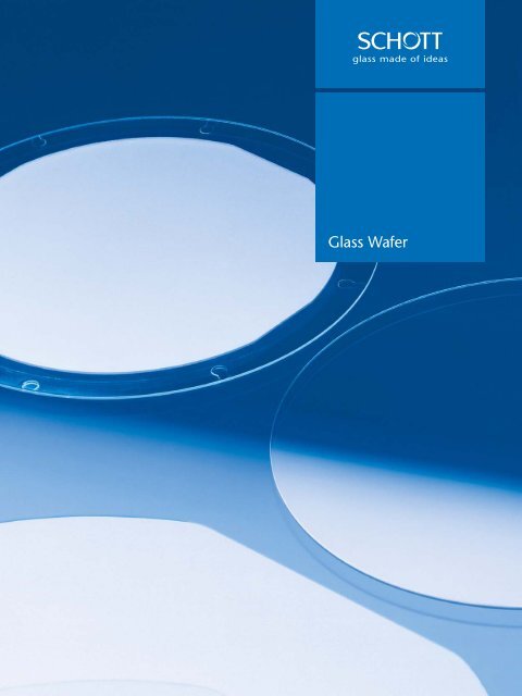
Glass Wafer
- Page 2 and 3: 2 SCHOTT is an international techno
- Page 4: 4 Typical Applications Wafers are u
- Page 7 and 8: Down-Draw Process The key character
- Page 9 and 10: D 263 ® T eco Thin Glass Specifica
- Page 11 and 12: MEMpax ® Specifications Applicatio
- Page 13 and 14: Main Competences in Glass Wafer Pro
- Page 15 and 16: Table 2 Process capabilities Edge T
- Page 18 and 19: 18 Wafer Manufacturing Network Adva
- Page 20: Advanced Optics SCHOTT North Americ
<strong>Glass</strong> <strong>Wafer</strong>
2<br />
<strong>SCHOTT</strong> is an international technology group with more than 125 years<br />
of experience in the areas of specialty glasses, materials and advanced<br />
technologies. With our high-quality products and intelligent solutions,<br />
we contribute to our customers’ success and make <strong>SCHOTT</strong> part of<br />
everyone’s life.<br />
<strong>SCHOTT</strong> Advanced Optics, with its deep technological expertise, is<br />
a valuable partner for its customers in developing products and cus-<br />
tomized solutions for applications in optics, lithography, astronomy,<br />
opto-electronics, life sciences, and research. With a product portfolio<br />
of more than 100 optical glasses, special materials and components,<br />
we master the value chain: from customized glass development to<br />
high-precision optical product finishing and metrology.<br />
<strong>SCHOTT</strong>: Your Partner for Excellence in Optics.<br />
Figure 1<br />
<strong>Wafer</strong> with Notch
Unique <strong>Wafer</strong> Portfolio with Solutions for Your Applications<br />
As “Your Partner for Excellence in Optics” Advanced Optics holds very close relationship with its customers and develops<br />
solutions and products reflecting the market’ needs.<br />
This is a reason why <strong>SCHOTT</strong> is today the world’s leading supplier of thin and ultra thin glass wafers made of different<br />
materials in sizes between 4” and 12” with different surface qualities and customized features.<br />
Applying proprietary production processes, leveraging a selection of different materials and the continuous expansion of<br />
state-of-the-art processing capabilities make our wafer-offerings unique in the industry.<br />
Our wafer-offerings and processing technologies are presented in this catalog.<br />
3
4<br />
Typical Applications<br />
<strong>Wafer</strong>s are used in a great variety of applications within<br />
the Semiconductor, Electronics and Biotech industry.<br />
<strong>Wafer</strong>s can be found in nearly every CMOS (complemen-<br />
tary metal oxide semiconductor) or CCD (charges coupled<br />
device) image sensor in the market of smart phones, tablet<br />
PCs and digital cameras. The combination of semiconductor<br />
image sensors and <strong>SCHOTT</strong> glass wafers in state-of-the-art<br />
packaging technologies such as <strong>Wafer</strong> Level Chip Size<br />
Packaging (WLCSP) meets the demands for smallest form<br />
factors and highest quality levels.<br />
Thin glass wafers are also used as carrier substrates and<br />
spacers for compact and cost efficient lens systems. For other<br />
applications like MEMS (micro electro mechanical systems)<br />
sensors in automotive and consumer products <strong>SCHOTT</strong> is<br />
supplying structured glass wafers with holes or cavities to<br />
meet the specific needs of those products.<br />
Figure 2<br />
Structured glass wafer
6<br />
Thin <strong>Glass</strong> at <strong>SCHOTT</strong><br />
<strong>SCHOTT</strong> has a long standing history in producing thin glass and developed various proprietary production processes.<br />
The thinnest glass substrates available from <strong>SCHOTT</strong> are less than 50 µm in thickness and will soon be even commercially<br />
available on a reel.<br />
This expertise forms the principle pillar for being the leading supplier for <strong>Wafer</strong>s. The relevant materials for our wafer-<br />
offerings are made in a special down-draw process. Detailed characteristics of these glass types (AF 32 ® eco, D 263 ® T eco,<br />
MEMpax ® ) are presented on the following pages.<br />
<strong>SCHOTT</strong> is also contributing to environmental safety and sustainability and offers the “green”<br />
glass types AF 32 ® eco and D 263 ® T eco from a melting process which does not utilize any hazardous<br />
refining agents.<br />
Through offering such eco glass types <strong>SCHOTT</strong> has done a major step in supporting the realization<br />
of “green” end-user products.
Down-Draw Process<br />
The key characteristics of the down-draw process<br />
(AF 32 ® eco, D 263 ® T eco, MEMpax ® ) are:<br />
• Fire-polished surface with surface roughness < 1 nm<br />
• Wide thickness range, from 1.1 mm down to 25 µm<br />
• Fast changeover between different glass types<br />
• High flexibility regarding throughput and thickness<br />
Figure 3<br />
Thin glass (50 μm)<br />
Figure 4<br />
Down-Draw process at <strong>SCHOTT</strong><br />
Molten glass<br />
Roller<br />
Annealing<br />
furnace<br />
Roller<br />
<strong>Glass</strong> ribbon<br />
7
8<br />
AF 32 ® eco<br />
Thin <strong>Glass</strong><br />
Specifications<br />
Applications<br />
Forms of Supply<br />
Technical Data<br />
Dimensions<br />
Round and square custom size wafer<br />
formats, e. g. 6“, 8“ or 12“<br />
Thickness 0.03 mm up to 1.1 mm<br />
Luminous transmittance τ vD65 (d = 0.5 mm) 91.9 %<br />
Coefficient of mean linear thermal expansion<br />
α (20 °C; 300 °C) (static measurement)<br />
Transformation temperature T g<br />
Dielectric constant ε r at 1 MHZ 5.1<br />
Refractive index n D<br />
3.2 · 10 –6 K –1<br />
717 °C<br />
1.5099<br />
Density ρ (annealed at 40 °C/h) 2.43 g/cm 3<br />
• CTE matching silicon<br />
• High transmittance<br />
• Fire-polished surface with low roughness<br />
• Environmentally friendly production without hazardous refining agents<br />
• <strong>Wafer</strong> Level Chip Size Packaging<br />
• <strong>Wafer</strong> Level Optics<br />
• Microsheet<br />
• <strong>Wafer</strong> from 4“ to 12“ diameter<br />
• Sheet up to 300 mm x 300 mm<br />
• Microsheet on reel (sampling)
D 263 ® T eco Thin <strong>Glass</strong><br />
Specifications<br />
Applications<br />
Forms of Supply<br />
Technical Data<br />
Dimensions<br />
440 mm x 360 mm, other size<br />
on request<br />
Thickness 0.03 mm up to 1.1 mm<br />
Luminous transmittance τvD65 (d = 1.1 mm) 91.7 %<br />
Coefficient of mean linear thermal expansion<br />
α (20 °C; 300 °C) (static measurement)<br />
7.2 · 10 –6 K –1<br />
Transformation temperature Tg 557 °C<br />
Dielectric constant εr at 1 MHZ 6.7<br />
Refractive index nD 1.5230<br />
Density ρ (annealed at 40 °C/h) 2.51 g/cm3 • High chemical resistance<br />
• Stable against sunlight and heat<br />
• High luminous transmittance<br />
• Environmentally friendly production without hazardous refining agents<br />
• Resistive touch panel applications<br />
• Substrate glass for IR cut-off filter for camera modules in mobile phones<br />
• Microsheet<br />
• Wide range of thicknesses<br />
• Variety of in-stock sizes and shapes<br />
• Microsheet on reel (sampling)<br />
9
10<br />
Figure 5<br />
Structured wafer for sensor application
MEMpax ®<br />
Specifications<br />
Applications<br />
Forms of Supply<br />
Technical Data<br />
Dimensions 6”, 8” or 12” <strong>Wafer</strong><br />
Thickness 0.1 mm to 1.1 mm<br />
Luminous transmittance τ vD65 (d = 0.5 mm) 91,7 %<br />
Coefficient of mean linear thermal expansion<br />
α (20 °C; 300 °C) (static measurement)<br />
3.25 · 10 –6 K –1<br />
Transformation temperature Tg 525 °C<br />
Dielectric constant εr at 1 MHZ 4.6<br />
Refractive index n D<br />
1.4714<br />
Density ρ (annealed at 40 °C/h) 2.2 g/cm 3<br />
• Fire-polished surface<br />
• CTE matching silicon<br />
• High thermal stability<br />
• Enabling anodic bonding with silicon wafers<br />
• Excellent transmission<br />
• Physical and chemical properties identical with Borofloat ® 33<br />
• MEMS<br />
• <strong>Wafer</strong> level packaging<br />
• Biotechnology<br />
• Optical sensors<br />
• Lighting solutions<br />
• 6“, 8“ or 12“ wafer<br />
11
12<br />
Figure 6<br />
Structured glass wafer
Main Competences in <strong>Glass</strong> <strong>Wafer</strong> Processing<br />
Besides offering wafers made of different materials and different sizes <strong>SCHOTT</strong> has built up extensive experiences and<br />
know-how in glass processing.<br />
Learning from a <strong>SCHOTT</strong> history of glass melting and processing of more than 125 years and leveraging a strong network<br />
with experts and partners <strong>SCHOTT</strong> is able to offer wafers in almost any customized structure, surface quality and with<br />
individual features. This makes our products unique!<br />
Here you find an overview, details of our competencies are gives on the following pages.<br />
Process capabilities<br />
Cutting<br />
• Laser or Diamond Cutting<br />
• <strong>Wafer</strong> sizes 4“ – 12“ (round)<br />
• Substrates up to 400 x 500 mm<br />
Edge Treatment<br />
• Flat or Notch<br />
• C- or facet shape<br />
• Seaming<br />
Surface Refinement<br />
• Polishing or Lapping<br />
• Coating<br />
Structuring<br />
• Ultrasonic Lapping<br />
• Powder Blasting<br />
Washing Process<br />
• Ultrasonic Washing<br />
• End cleaning with DI water<br />
Clean Room Packaging<br />
• Clean Room Production<br />
• Inspection and Measurement under Clean Room Conditions<br />
• Packaging into flow boxes<br />
13
14<br />
Our Competencies in Detail<br />
Polishing<br />
Table 1<br />
Options for polishing<br />
Structuring<br />
Figure 7<br />
Sonotrode<br />
Figure 8<br />
Structured substrate<br />
With our state-of-art polishing operations and long experience in polishing of thin<br />
glass, we can meet and exceed all industry standards and customer requirements.<br />
Properties Fire polishing Standard polishing Advanced polishing<br />
Materials<br />
Edge grinding<br />
AF 32 ® eco<br />
D 263 ® T eco<br />
MEMpax ®<br />
Cut<br />
C-shape<br />
Facet<br />
AF 32 ® eco<br />
D 263 ® T eco<br />
BOROFLOAT ® 33<br />
C-shape<br />
Facet<br />
AF 32 ® eco<br />
D 263 ® T eco<br />
BOROFLOAT ® 33<br />
C-shape<br />
Facet<br />
Notch Possible Possible SEMI<br />
TTV ≤ 5 µm ≤ 10 µm < 2 µm to 5 µm<br />
Flatness (warp)<br />
Depending on<br />
raw material<br />
Roughness (Ra) < 0.8 nm < 2 nm<br />
Surface defects<br />
(Scratch / Digs)<br />
according to<br />
MIL-PRF 13830B<br />
≥ 5/1 to 10/5<br />
(cut 40/10)<br />
≥ 20 µm 10 µm to 20 µm<br />
≥ 10/5 to 20105<br />
≥ 5/1 to 10/5<br />
(> 3 µm to 5 µm visible)<br />
≥ 5/1 to 10/5<br />
(> 3 µm to 5 µm visible)<br />
With the Powder blasting technology and the Ultrasonic lapping process <strong>SCHOTT</strong><br />
has established a variety of capabilities to provide specific solutions for structured<br />
glass wafers.
Table 2<br />
Process capabilities<br />
Edge Treatment<br />
Options for edge processing<br />
Ultrasonic lapping Powder blasting<br />
Size 100 mm to 200 mm Max. 400 mm x 400 mm<br />
Thickness range 0.4 mm up to 3 mm 0.05 mm up to 3 mm<br />
Different hole configurations Round holes<br />
Round, rectangular holes<br />
and caverns<br />
Positioning tolerances ± 65 µm* ± 65 µm*<br />
Min. hole diameter 0.4 mm 0.1 mm<br />
* Tighter tolerances on request<br />
Our expertise in edge treatment offers the choice between flat and notch<br />
orientation marking according SEMI industry standards. <strong>Wafer</strong> edges can be<br />
processed to C-shape or facet shape.<br />
Flats<br />
C-Shape<br />
Notches<br />
Facet Shape<br />
15
16<br />
Ultra Sonic Washing<br />
Our expertise in ultra sonic washing under clean room<br />
conditions enables us to provide highest precision and to<br />
deliver products into the semiconductor industry.<br />
Key characteristics of the washing process<br />
• High cleaning results with sour and alkaline cleaner<br />
• End cleaning with DI-Water<br />
• Drying with Infrared lamps<br />
• Situated in a clean-room (Class 1000) and packaged<br />
in flowboxes (class 100)<br />
Out side<br />
feed in<br />
station<br />
Clean Room class 1000<br />
1<br />
process ow<br />
Clean Room Packaging<br />
2 3 4 5 6 7 8 9<br />
We have the capability of Clean Room Production<br />
where all wafers are inspected under clean room<br />
conditions (class 1000) using special measurement<br />
and testing instrumentation. <strong>Wafer</strong>s can be packed<br />
in wafer shipment boxes (flow boxes) and under clean<br />
room condition.<br />
Figure 9<br />
Ultra sonic washing process<br />
Figure 10<br />
Carrier with structured glass wafers<br />
additional clean room benches<br />
IR-drying buffer
18<br />
<strong>Wafer</strong> Manufacturing Network<br />
Advanced Optics<br />
<strong>SCHOTT</strong> AG<br />
Mainz, Germany<br />
Headquarter, R & D,<br />
Product Management<br />
<strong>SCHOTT</strong> <strong>Glass</strong> Malaysia Sdn. Bhd.<br />
<strong>SCHOTT</strong> <strong>Glass</strong> Malaysia Components Sdn. Bhd.<br />
Perai, Penang, Malaysia<br />
<strong>Wafer</strong> Processing, Polishing, Structuring<br />
Advanced Optics<br />
<strong>SCHOTT</strong> AG<br />
Grünenplan, Germany<br />
Production & Thin <strong>Glass</strong><br />
Competence Center<br />
<strong>SCHOTT</strong><br />
Customer Service &<br />
Technology Center<br />
China, Japan
Quality Assurance<br />
Quality control is based on statistical process control, as well as on rigorous final<br />
inspection of the finished component. <strong>Glass</strong> properties are measured for every<br />
melt. Measurement instruments include a broad range of interferometers,<br />
spectrophotometers, physical property test systems, vision systems, and a laser<br />
test bed.<br />
Figure 11<br />
EN ISO 9001:2008 Certificate<br />
19
Advanced Optics<br />
<strong>SCHOTT</strong> <strong>North</strong> <strong>America</strong>, Inc.<br />
400 York Avenue<br />
Duryea, PA 18642<br />
USA<br />
Phone: 1-570-457-7485<br />
Fax: 1-570-457-7330<br />
info.optics@us.schott.com<br />
www.us.schott.com/advanced_optics<br />
10364 ENGLISH-USA 01120.25 kn/odd Printed in Germany


