Technology Trends—Fourth Quarter 1986
Technology Trends—Fourth Quarter 1986
Technology Trends—Fourth Quarter 1986

You also want an ePaper? Increase the reach of your titles
YUMPU automatically turns print PDFs into web optimized ePapers that Google loves.
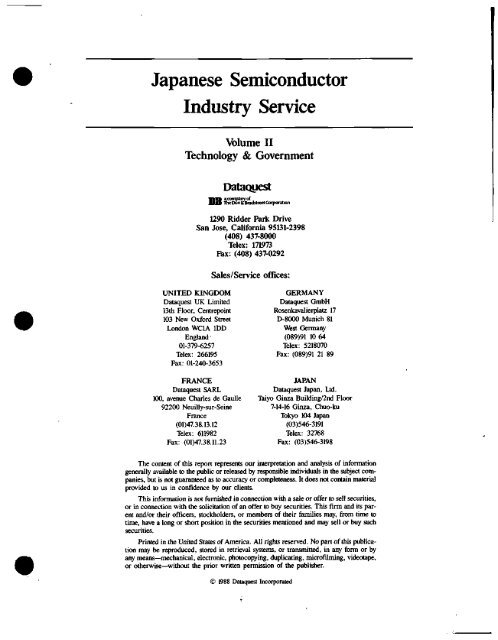
Japanese Semiconductor<br />
Industry Service<br />
Volume II<br />
<strong>Technology</strong> & Government<br />
Dataquest<br />
n n a company of<br />
The Dun & Bradstreet Corporation<br />
1290 Ridder Park Drive<br />
San Jose, California 95131-2398<br />
(408) 437-8000<br />
Telex: 171973<br />
Fax: (408) 437-0292<br />
Sales/Service offices:<br />
UNITED KINGDOM GERMANY<br />
Dataquest UK Limited Dataquest GmbH<br />
13th Floor, Centrepoint Rosenkavalierplatz 17<br />
103 New Oxford Street D-8000 Munich 81<br />
London WCIA IDD West Germany<br />
England (089)91 10 64<br />
01-379-6257 Telex: 5218070<br />
Telex: 266195 Fax: (089)91 21 89<br />
Fax: 01-240-3653<br />
FRANCE JAPAN<br />
Dataquest SARL Dataquest Japan, Ltd.<br />
100, avenue Charles de Gaulle Taiyo Ginza Building/2nd Floor<br />
92200 Neuilly-sur-Seine 7-14-16 Ginza, Chuo-ku<br />
France Tokyo 104 Japan<br />
(01)4738.13.12 (03)546-3191<br />
Telex: 611982 Telex: 32768<br />
Fax: (01)4738.11.23 Fax: (03)546-3198<br />
The content of this report represents our interpretation and analysis of information<br />
generally available to the public or released by responsible individuals in the subject companies,<br />
but is not guaranteed as to accuracy or completeness. It does not contain material<br />
provided to us in confidence by our clients.<br />
This information is not furnished in connection with a sale or offer to sell securities,<br />
or in connection with the solicitation of an offer to buy securities. This firm and its parent<br />
and/or their officers, stockholders, or members of their families may, from time to<br />
time, have a long or short position in the securities mentioned and may sell or buy such<br />
securities.<br />
Printed in the United States of America. All rights reserved. No part of this publication<br />
may be reproduced, stored in retrieval systems, or transmitted, in wny form or by<br />
any means—mechanical, electronic, photocopying, duplicating, microfilming, videotape,<br />
or otherwise—without the prior written permission of the publisher.<br />
© 1988 Dataquest Incorporated
Introduction to the Service<br />
The Japanese Semiconductor Industry Service (JSIS) docximents,<br />
analyzes, and interprets all important aspects of the Japanese<br />
semiconductor industry and the Japanese manufacturers that participate in<br />
the world markets. The service comprises;<br />
• Three loose-leaf data base binders containing sections that are<br />
continuously revised and updated as developments occur or<br />
additional information becomes available<br />
• Timely newsletters reporting on significant industry<br />
developments—additional binders are provided for these<br />
newsletters<br />
• I.e. ASIA> a semimonthly report on the Japanese and Asian<br />
integrated circuit industry, and I.C. USA, a semimonthly report<br />
on the U.S. integrated circuit industry, focusing on start-ups,<br />
strategic alliances, and government activity<br />
• Direct access to research staff in Tokyo and San Jose for<br />
background information and questions pertaining to information<br />
contained in each volume<br />
The service analyzes, interprets, and reports on the products,<br />
markets, and strategies of the major Japanese companies in the<br />
semiconductor industry, with a specific focus on the Japanese market.<br />
This service also presents valuable information on Japanese government,<br />
economy, and industrial policy, and will provide periodic pertinent<br />
updates to these subjects. JSIS provides data with which to make<br />
strategic decisions. We perform the following functions:<br />
• Track Japanese semiconductor production, inventory, shipments,<br />
exports, imports, and consumption for the major products<br />
• Forecast 10-year consumption figures for all semiconductor<br />
categories<br />
• Examine and analyze the consumer and industrial electronics<br />
end-user markets<br />
• Analyze trends in CAD tools and plant automation<br />
• Analyze trends in strategic alliances<br />
JSIS Volume II O 1987 Dataquest Incorporated April
Introduction to the Service<br />
Monitor Japanese R&D projects and corporate spending for the<br />
following areas:<br />
Semiconductors<br />
Computers<br />
Telecommunications<br />
Issue periodic reports on trends in patent applications and<br />
technical papers<br />
Analyze semiconductor technology trends on a quarterly basis<br />
Evaluate plant capacity expansion and design center activity<br />
Profile the major Japanese semiconductor companies, emphasizing<br />
their products and strategies<br />
Analyze the forces affecting the Japanese semiconductor markets<br />
Investigate the fundamental operation of Japanese industries<br />
Dataquest monitors the Japanese Semiconductor Industry using the<br />
system shown in Figure 1. Generally, we observe that RStD projects<br />
precede new products by four to eight years; technical papers and patents<br />
precede new products by three to four years.<br />
e 1987 Dataquest Incorporated April JSIS Volume II
C4<br />
01<br />
H<br />
m<br />
<<br />
o<br />
\o<br />
00<br />
O<br />
P)<br />
ft<br />
lO<br />
o<br />
u<br />
ft<br />
n<br />
o<br />
»d<br />
o<br />
•i<br />
PI<br />
ft<br />
(D<br />
0><br />
•1<br />
ita<br />
R&D<br />
Spending<br />
Corporate<br />
R&D<br />
Government<br />
R&D<br />
Industrial<br />
Policy<br />
• Taxes<br />
• Financing<br />
> Tectinopolis<br />
Patents<br />
Technical<br />
Papers<br />
Figure 1<br />
JAPANESE SEMICONDUCTOB INDUSTBY ANALYSIS<br />
•<br />
Capital<br />
Spending<br />
<strong>Technology</strong><br />
Trends<br />
CAD Tools<br />
Equipment<br />
Automation<br />
Rant<br />
Capacity<br />
Consumption<br />
Forecast<br />
,<br />
New Products<br />
,<br />
Strategic<br />
Alliances<br />
Major Users<br />
End Use<br />
Consumption<br />
Production<br />
Inventory<br />
•<br />
impons/<br />
Exports<br />
. 1<br />
Distribution<br />
_ 1<br />
Shipments<br />
,<br />
Company<br />
Profiles
HEED FOR THE SERVICE<br />
Introduction to the Service<br />
Since 1975, Dataquest's Semiconductor Industry Service has offered<br />
comprehensive worldwide market research to semiconductor manufacturers,<br />
semiconductor users, and suppliers of semiconductor manufacturing<br />
equipment and materials. As individual geographical markets expanded, it<br />
became obvious that each of these areas was developing its own unique<br />
characteristics. This was especially true of Japan, since it has become<br />
a major industrial power and, in fact, has attained the number one<br />
position in the world for merchant market semiconductor unit and value<br />
production.<br />
Much has been written on the Japanese, but there is no other single<br />
detailed, comprehensive, continuously updated and unbiased analytical<br />
service in the semiconductor market. With the movement of both finished<br />
and unfinished semiconductor products across geographical borders,<br />
available industry statistics sources have become less useful. Hence,<br />
there is a growing need for the type of data that Dataquest provides<br />
through its continuous industry coverage, updated data base, and analyses<br />
of observed trends.<br />
SERVICE STROCTORE AMD TERMINOLOGY<br />
Detailed discussions of semiconductor consumption, production, and<br />
shipments are broken out in three ways:<br />
• Product technology<br />
• Product function for integrated circuits<br />
• End-user market<br />
Product TechnolooY<br />
Total S«niconductor<br />
• Integrated Circuits<br />
Bipolar digital—This category includes all monolithic<br />
bipolar digital logic and memory devices.<br />
MOS—This includes all monolithic digital MOS memory and<br />
logic devices; this total is further divided into PMOS,<br />
MMOS, and CMOS.<br />
O 1987 Dataquest Incorporated April JSIS Volume II
Discrete<br />
Introduction to the Service<br />
Linear—This includes all linear integrated circuits;<br />
hybrids manufactured and packaged by the same company are<br />
included.<br />
Transistors<br />
* Small-signal transistors—Silicon or germanitim<br />
transistors with a power dissipation of less than one<br />
watt; includes all radio frequency and microwave<br />
small-signal transistors, dual transistors, fieldeffect<br />
transistors, and general-purpose bipolar signal<br />
transistors<br />
. Power transistors—Silicon or germaniiim transistors<br />
with a power dissipation of one watt or more; includes<br />
radio frequency and microwave power transistors and<br />
Darlington power transistors<br />
Diodes<br />
Small-signal diodes—All diodes rated at less than one<br />
ampere; includes microwave diodes, varactor tuning<br />
diodes, tunnel diodes, and discrete rectifiers<br />
Power diodes—All diodes rated at more than one<br />
ampere; includes all discrete rectifiers and<br />
assemblies thereof with current ranges of more than<br />
one ampere, selenium rectifiers, and other<br />
polycrystalline devices<br />
, Zener diodes~All voltage reference and regulator<br />
diodes<br />
Thyristors—Includes all unidirectional and bidirectional<br />
thyristors<br />
Other discrete—Includes all discrete devices not<br />
specifically classified above<br />
Optoelectronics—This group is further divided into LED lamps,<br />
LED displays (single- or multidigit), couplers, and other. The<br />
"other" category includes photo transistors, photo diodes, photo<br />
conductive devices, and infrared lamps. Not included are solar<br />
cells, liquid crystal devices and displays, and incandescent<br />
lamps and displays.<br />
JSIS Volume II O 1987 Dataquest Incorporated April
Introduction to the Service<br />
Product yy^^t-ion for Integrated Circuits<br />
• Total bipolar digital ICs<br />
Memory<br />
Logic<br />
• Total MOS digital ICs<br />
Memory<br />
Micro devices<br />
Logic<br />
• Total linear ICs<br />
End-User MarXet<br />
• Consumer electronics<br />
Video<br />
Audio<br />
Home appliances<br />
• Industrial electronics<br />
Computers<br />
Commercial peripherals<br />
Word processors<br />
Communication<br />
Industrial<br />
Transportation<br />
9 1987 Dataguest Incorporated April JSIS Volume II
SERVICE ORGANIZATIOH<br />
Introduction to the Service<br />
Throughout the JSIS three-ring binders, the terms factory shipments<br />
and production are particularly significant when used in conjunction with<br />
geographical regions. The term factory shipments refers to devices<br />
produced and shipped in a particular region, but the term production<br />
refers to the country in which a company has its headquarters. For<br />
example, devices produced by an Hitachi subsidiary in the United States<br />
would be counted in U.S. factory shipments, but would also be counted as<br />
part of the Japanese companies' total production.<br />
Volume I—Markets<br />
Volume I contains specifics of the semiconductor industry both in<br />
Japan and overseas. It is divided into the following sections:<br />
• History of the Industry—Discusses the history of the industry,<br />
distribution and sales channels to the market, production, and<br />
productivity figures<br />
• Production/Consiimption—Contains Japeuiese semiconductor shipments,<br />
production, consiimption history, and consumption forecasts<br />
• Market Share Estimates—Contains worldwide shares for the major<br />
Japanese manufacturers and market shares in Japan for the major<br />
Japanese, U.S., European, and Rest of World manufacturers<br />
• Exports/Imports—Analyzes Japanese exports, imports, and balance<br />
of trade in the major semiconductor families, particularly<br />
emphasizing trade between the United States and Japan<br />
• Market Access—Analyzes history and status of the U.S.-Japan<br />
Semiconductor Trade Arrangement; also includes monthly<br />
statistics on selected electronic equipment markets in Japan,<br />
such as copiers, personal computers, and DAS players<br />
• Semiconductor End Use—Analyzes the major semiconductor products<br />
that are used in the consumer and industrial markets and the<br />
major subsections of those markets; explores specific<br />
application trends such as VTRs, personal computers, robotics,<br />
and facsimile machines; examines who buys what and how much<br />
• Distribution—Analyzes trends in Japanese semiconductor sales<br />
through distribution; explains who the major distributors are;<br />
examines differences between distribution in Japan and the<br />
United States<br />
JSIS Volume II O 1987 Dataquest Incorporated April
Introduction to the Service<br />
Electronics Industry—Provides an overview of the Japanese<br />
electronics industry, including the increasing part that the<br />
electronics industry plays in Japan; includes annual production<br />
forecast and history of 50 specific categories of electronic<br />
equipment<br />
Volume II—Tef^^^rtni ntjY anri fiovemment<br />
Volume II of JSIS contains separate sections for each of the<br />
following:<br />
<strong>Technology</strong>—Discusses major trends in Japanese semiconductor<br />
technology<br />
Strategic Alliances—Analyzes joint venture, licensing, and<br />
second-sourcing agreements entered by Japanese semiconductor<br />
device and equipment makers<br />
Start-ups/Newcomers—Reviews trends among semiconductor start-up<br />
companies and major Japanese companies entering the industry<br />
Corporate R&D—Evaluates trends in corporate R&D spending and<br />
the opening of new basic research laboratories<br />
Government R&D—Reviews the major national R&D projects covering<br />
semiconductors, computers, and telecommunications<br />
Industrial Policy—Explores MITI's administrative guidance of<br />
industry. Discusses MITI's relationship with the hightechnology<br />
industries, with details on the growth of specific<br />
strategic industries<br />
INS Program—Describes Nippon Telegraph and Telephone's<br />
Information Network System (INS) development plans<br />
Technopolis Sites—Reviews the 19 high-technology research<br />
cities planned by MITI<br />
Design Centers/ASICs—Analyzes trends among Japanese vendors and<br />
design centers<br />
CAD Tools/Artificial Intelligence—Examines CAD trends and the<br />
growing use of expert systems in VLSI<br />
Plant Capacity—Analyzes plemt capacity additions in Japan and<br />
lists semiconductor plants, by company<br />
e 1987 Dataquest Incorporated April JSIS Volume II
Introduction to the Service<br />
• Economy—Presents macroeconomic statistics on industrial<br />
production, capacity utilization, exports, imports, balance of<br />
payments, plant and equipment expenditures, wholesale and<br />
consumer prices, inventories, and financial data for the major<br />
industries<br />
Volume III—Companies<br />
The third volume includes profiles of major Japanese merchant<br />
semiconductor companies, including analyses of sales channels, financial<br />
structure, and product portfolios. It also includes examinations of<br />
factory locations, their technologies, and their organizational<br />
structures. Semiconductor revenues for most companies are split by<br />
geographical region.<br />
The companies covered include:<br />
Fuji Electric<br />
Fujitsu<br />
Hitachi<br />
Matsushita<br />
Mitsubishi<br />
NEC<br />
NTT<br />
Oki<br />
Rohm<br />
Sanken<br />
Sanyo<br />
Seiko Epson<br />
Sharp<br />
Sony<br />
Toshiba<br />
JSIS Volume II 9 1987 Dataquest Incorporated April
SERVICE FEATDHES AMD PROCEDURES<br />
Introduction to the Service<br />
The date of preparation is noted on the bottom of each page o£ a<br />
document. Sections are updated on a regular basis, and filing instructions<br />
are sent with the new versions. A complete table of contents is<br />
produced on a regular basis to enable you to verify that your binders are<br />
current and complete.<br />
Newsletters are published at monthly intervals and should be filed in<br />
the Newsletter binder. The newsletters are devoted to current topics of<br />
specific Japanese interest and to international industry developments.<br />
The inquiry privilege permits the binderholder to contact Dataquest<br />
by mail, fax, telegram, telephone, telex, or in person to request copies<br />
of printed material, data, or opinions on topics covered by the Japanese<br />
Semiconductor Industry Service staff. The principal information<br />
collections are maintained at our San Jose, California, headquarters and,<br />
with the exception of confidential or proprietary material, are available<br />
to all our subscribers. We also have a research staff in Tokyo that<br />
maintains pertinent information on the material contained in the JSIS<br />
data base.<br />
10 e 1987 Dataquest Incorporated April JSIS Volume II
DATAQUEST LOCATIONS<br />
Introduction to the Service<br />
The Japanese Semiconductor Industry Service (JSIS) has its<br />
headquarters in our San Jose, California, office. Clients in Europe, the<br />
United States, or Latin America should address their inquiries to this<br />
headquarters office. JSIS also maintains a staff in our Tokyo office;<br />
inquiries from subscribers in Japan and Asia should be addressed to our<br />
Tokyo office.<br />
Dataquest Incorporated<br />
1290 Ridder Park Drive<br />
San Jose, CA 95131-2398<br />
Telephone: (408) 971-9000<br />
Telex: 171973<br />
Fax: (408) 971-9003<br />
Dataquest UK Limited<br />
13th Floor, Centrepoint<br />
103 New Oxford Street<br />
London WCIA IDD<br />
England<br />
Telephone: (01)379-6257<br />
Telex: 266195<br />
Fax: (01)240-3653<br />
Dataquest Taiwan<br />
Room 801, 8th Floor,<br />
Ever Spring Building<br />
147, Sec. 2, Chien Kuo N. Road<br />
Taipei, Taiwem, R.O.C. 104<br />
Telephone: (02)501-7960/501-5592<br />
Telex: 27459<br />
Fax: (02)505-4265<br />
Dataquest Japan, Limited<br />
Taiyo Ginza Building/2nd Floor<br />
7-14-16, Ginza, Chuo-ku<br />
Tokyo 104 Japan<br />
Telephone: (03)546-3191<br />
Telex: J32768<br />
Fax: (03)546-3198<br />
Dataquest SARL<br />
100, Avenue Charles de Gaulle<br />
92200 Neuilly-sur-Seine<br />
France<br />
Telephone: (01)47.38.13.12<br />
Telex: 611982<br />
Fax: (01)47.38.11.23<br />
Dataquest GmbH<br />
Rosenkavalierplatz 17<br />
D-8000 Munich 81<br />
West Germany<br />
Telephone: (089) 91 1064<br />
Telex: 5218070<br />
Fax: (089)91 21 98<br />
JAPANESE SEMXCOMPnCTOR IMDUSTRY SERVICE STAFF CAPABILITIES<br />
The Dataquest Japanese Semiconductor Industry Service staff has a<br />
continuing, long-term commitment to the semiconductor and related<br />
electronic industries. The expertise and experience of the worldwide<br />
Semiconductor Industry Service staff and access to the resources of other<br />
Dataquest high-technology industry groups further enhances the quality of<br />
our service.<br />
JSIS Volume II 9 1987 Dataquest Incorporated April 11
Introduction to the Service<br />
Members of Dataguest's professional staff are freguent speakers at<br />
industry seminars and symposia. We participate in the leading<br />
professional societies related to the electronics industry. We maintain<br />
contact with a large user base through sophisticated sampling and<br />
interviewing technigues. Our staff regularly reviews all important<br />
publications related to the semiconductor industry and associated user<br />
industries.<br />
SERVICE STAFF<br />
Gene Norrett<br />
Mr. Norrett is Vice President and<br />
Director of Dataguest's Semiconductor<br />
Industry Group. Mr. Norrett is based in<br />
the Dataguest corporate headguarters<br />
and directs research staffs in the<br />
San Jose and Tokyo offices. Prior to<br />
joining Dataguest, Mr. Norrett spent<br />
14 years with the Motorola<br />
Semiconductor Group, serving in various<br />
marketing and management positions. He<br />
was most recently Manager of Market<br />
Research, where he was responsible for<br />
research analysis of worldwide<br />
semiconductor industry trends. In this<br />
capacity, he served as the company's<br />
representa> tive to the Semiconductor<br />
Industry Association and was Chairman<br />
of the Association's Trade Statistics<br />
Committee. Mr. Norrett has traveled<br />
extensively in Japan, Hong Kong,<br />
Taiwan, Korea, China, and Europe and<br />
has developed an awareness and thorough<br />
understanding of their semiconductor<br />
markets. His educational background<br />
includes a B.A. degree in Mathematics<br />
from Temple University and an<br />
M.Se degree in Applied Statistics from<br />
Villanova University. He has also<br />
taken graduate courses in marketing<br />
from Arizona State University.<br />
12 O 1987 Dataguest Incorporated April JSIS Volume II
Introduction to the Service<br />
Osamu Ohtake<br />
Mr. Ohtake is the Tokyo-based Associate<br />
Director for Dataguest's Japanese<br />
Semiconductor Industry Service and is<br />
responsible for strategic research on<br />
technologies, markets, products, and<br />
manufacturers. Prior to joining<br />
Dataquest, Mr. Ohtake worked for<br />
10 years as a reporter and then most<br />
recently as Components Group Manager<br />
for Dempa Shimbun. a daily electronics<br />
industry newspaper published in Japan.<br />
He has also authored reports on the<br />
Japanese VLSI project and on semiconductor<br />
materials and equipment markets.<br />
A native of Japan, Mr. Ohtake is a<br />
graduate of Tokyo Denki University,<br />
specializing in telecommunications.<br />
Sheridan M. Tatsuno<br />
Mr. Tatsuno is a Senior Industry<br />
Analyst working for Dataguest's<br />
Japanese Semiconductor Industry<br />
Service. He is responsible for<br />
analyzing trends in Japanese government<br />
policies, procurement, financial<br />
markets, industrial financing,<br />
subsidized R&D, overall economics, and<br />
industrial plant siting. Prior to<br />
joining Dataquest, he had seven years<br />
of experience in market research,<br />
planning, and international finance<br />
with Bechtel and Hoodward-Clyde<br />
Consultants, Mr. Tatsuno has a<br />
B.A. degree in Political Science from<br />
Yale University and a Master's degree<br />
in Planning and Policy Analysis from<br />
Harvard University's Kennedy School of<br />
Government. In addition to these<br />
credentials, Mr. Tatsuno is fluent in<br />
Japanese, French, and Spanish.<br />
JSIS Volume II e 1987 Dataquest Incorporated April 13
Introduction to the Service<br />
Patricia S. Cox<br />
Mrs. Coz is an Industry Analyst for<br />
Dataguest's Japanese Semiconductor<br />
Industry Service and Product Manager for<br />
the semimonthly I.C. ASIA and I.C. USA<br />
newsletters. She is responsible for<br />
maintaining Japanese export, import,<br />
shipments, production, and consumption<br />
data; collecting market share data;<br />
performing in-depth company analyses;<br />
managing the computerized statistical<br />
data base; and performing general<br />
research duties. Mrs. Cox has five<br />
years of market research experience.<br />
Before joining Dataguest, Mrs. Cox was<br />
Contract Administrator at a New Jersey<br />
management information firm. Mrs. Cox<br />
received a Bachelor's degree and a<br />
Master's degree from Indiana University.<br />
Kazunori Hayashi<br />
Mr. Hayashi is an Industry Analyst for<br />
Dataguest's Japanese Semiconductor<br />
Industry Service and is based in<br />
Tokyo. He covers the semiconductor<br />
equipment and materials area. Among<br />
his responsibilities are researching<br />
and compiling the JSIS capacity<br />
analysis data base and updating the<br />
semiconductor equipment and materials<br />
data base.<br />
Prior to joining Dataguest, Mr. Hayashi<br />
was a co-founder of Innov Japan and<br />
Techno System Research Coporation. He<br />
has had 12 years experience in the<br />
industry. During this time, he has<br />
authored publications and performed<br />
research and consulting on the Japanese<br />
semiconductor equipment industry.<br />
Mr. Hayashi is a graduate of Meiji<br />
University in commercial sciences.<br />
14 O 1987 Dataguest Incorporated April JSIS Volume II
Introduction to the Service<br />
Nagayoshi Hakauo<br />
Mr. Nakano is a Research Analyst for<br />
Dataquest's Japanese Semiconductor<br />
Industry Service and is based in Tokyo.<br />
He is responsible for gathering information,<br />
researching, analyzing, and<br />
compiling the JSIS end-use data base,<br />
and providing general research support<br />
on the Japanese market. Prior to<br />
joining Oataquest, Mr. Nakano worked<br />
for six years as a journalist, most<br />
recently as associate editor for the<br />
foreign correspondent department of<br />
Dempa Shimbun. Japan's largest daily<br />
electronics industry newspaper.<br />
Mr. Nakano is a graduate of Doshisha<br />
University, Kyoto, where he majored in<br />
English Linguistics.<br />
Hideaki Nemoto<br />
Mr. Nemoto is a Research Associate for<br />
Dataquest's Japanese Semiconductor<br />
Industry Service and is based in Tokyo.<br />
He is responsible for the translation<br />
and editing of the Japanese-language<br />
I.e. USA newsletter, gathering MITI and<br />
Ministry of Finance statistics, handling<br />
client inquiries, and providing<br />
general research support on the<br />
Japanese market.<br />
Prior to joining Dataquest, Mr. Nemoto<br />
worked for two years as a foreign<br />
correspondent for Dempa Publications,<br />
Inc.<br />
Mr. Nemoto is a graduate of Doshisha<br />
University.<br />
JSIS Volume II e 1987 Dataquest Incorporated April 15
SUBSCRIPTION TERMS<br />
Basic Terms<br />
Introduction to the Service<br />
The Service begins on the date of the first billing. At that time,<br />
the notebook holder receives four service binders containing complete,<br />
up-to-date material and copies of all recent newsletters. Additionally,<br />
the notebook holder receives I.C. ASIA and I.C. USA binders. For the<br />
duration of the subscription, the notebook holder receives a copy of each<br />
additional or replacement section of the notebook and each newsletter<br />
published. Direct access to service staff may be used for questions<br />
related to the Japanese Semiconductor Industry Service.<br />
Ad^-Qg SvbgCriptJQns<br />
Subsidiaries, divisions, regional offices, majority-owned affiliates,<br />
and parent companies of the subscribing organization are eligible for<br />
add-on subscriptions at a fraction of the base price for each additional<br />
subscription.<br />
Relation^^ilp ^,o DATAOUEST's Semiconductor Industry Service<br />
The Japanese Semiconductor Industry Service (JSIS) is intended to<br />
complement the existing Semiconductor Industry Service (SIS), and topics<br />
of broad general interest such as discussions of technological advances<br />
will only be covered to the extent that they specifically affect Japan.<br />
These companion services are offered separately as components of<br />
Dataquest's international semiconductor industry program.<br />
Base Price and Payment Terms<br />
Industrial clients will be billed for the full price of the service<br />
on an annual basis. Dataquest reserves the right to raise its<br />
subscription prices to reflect broadened scope or increased costs.<br />
Subscribers will be notified in advance of any such price increase.<br />
16 e 1987 Dataquest Incorporated April JSIS Volume II
#<br />
^<br />
\<br />
f<br />
m
Title Page<br />
INTRODUCTION*<br />
Introduction to the Service<br />
TABLE OF CONTENTS<br />
TECHNOLOGY TRENDS<br />
Table of Contents<br />
JAPANESE SEMICONDUCTOR INDUSTRY SERVICE<br />
Volume II<br />
<strong>Technology</strong> <strong>Trends—Fourth</strong> <strong>Quarter</strong> <strong>1986</strong><br />
<strong>Technology</strong> Trends—Third <strong>Quarter</strong> <strong>1986</strong><br />
<strong>Technology</strong> Trends—Second <strong>Quarter</strong> <strong>1986</strong><br />
<strong>Technology</strong> Trends—First <strong>Quarter</strong> <strong>1986</strong><br />
EMERGING TECHNOLOGIES<br />
Emerging Office and Home Systems<br />
STRATEGIC ALLIANCES<br />
<strong>1986</strong> Japcinese Alliances<br />
1985 Japanese Alliances<br />
1984 Japanese Alliances<br />
STARTUPS/NEWCOMERS<br />
Semiconductor Start-Up History—1977-1985<br />
CORPORATE RSD<br />
New Japanese Research Labs<br />
•Titles in capital letters signify tabs<br />
JSIS Volume II © 1987 Dataquest Incorporated September
GOVERNMENT R&D<br />
Table of Contents<br />
JAPANESE SEMICONDUCTOR INDUSTRY SERVICE<br />
Government R&D Projects<br />
Optoelectronics Project<br />
Supercomputer Project<br />
Fifth-Generation Project<br />
Next-Generation Industries Program<br />
Future Electron Devices Project<br />
New Materials Project<br />
Bioelectronics Project<br />
Advanced Robotics Project<br />
INDUSTRIAL POLICY<br />
MXTI Organization<br />
MITI R&D Laboratories<br />
MITI Industrial Policies<br />
INS PROGRAM<br />
INS Program<br />
TECHNOPOLIS SITES<br />
PLANT CAPACITY<br />
Plant Robotics<br />
DESIGN CENTERS/ASICS<br />
Voltune II (Continued)<br />
•Titles in capital letters signify tabs<br />
1987 Dataquest Incorporated September JSIS Volume II
CAD TOOLS/AI<br />
CAD Tools/AI<br />
ECONOMY<br />
Economic Data and Outlook<br />
Table of Contents<br />
JAPANESE SEMICONDUCTOR INDUSTRY SERVICE<br />
Volume II (Continued)<br />
*Titles in capital letters signify tabs<br />
JSIS Volume II © 1987 Dataquest Incorporated September
Title Page<br />
INTRODUCTION*<br />
Introduction<br />
COMPANY PROFILES<br />
Company Profiles<br />
FUJI ELECTRIC<br />
FUJITSU<br />
HITACHI<br />
MATSUSHITA<br />
MITSUBISHI<br />
NEC<br />
NTT<br />
OKI-<br />
ROHM<br />
SANKEN<br />
SANYO<br />
SEIKO EPSON<br />
SHARP<br />
SONY<br />
TOSHIBA<br />
OTHER COMPANIES<br />
Table of Contents<br />
JAPANESE SEMICONDUCTOR INDUSTRY SERVICE<br />
Volume III<br />
•Titles in capital letters signify tabs<br />
1987 Dataquest Incorporated September JSIS Volume II
<strong>Technology</strong> Trends<br />
The following is a list of the material in this section:<br />
<strong>Technology</strong> Trends 1st <strong>Quarter</strong> <strong>1986</strong><br />
<strong>Technology</strong> Trends 2nd <strong>Quarter</strong> <strong>1986</strong><br />
<strong>Technology</strong> Trends 3rd <strong>Quarter</strong> <strong>1986</strong><br />
<strong>Technology</strong> <strong>Trends—Fourth</strong> <strong>Quarter</strong> <strong>1986</strong><br />
<strong>Technology</strong> Trends 1st <strong>Quarter</strong> 1987<br />
<strong>Technology</strong> Trends Second <strong>Quarter</strong> 1987<br />
NOTE: The arrow symbol indicates the latest documents's location behind<br />
this subject tab.<br />
JSIS Volume II ©1987 Dataquest Incorporated November ed,
SUMMARY<br />
<strong>Technology</strong> Trends<br />
1st <strong>Quarter</strong> <strong>1986</strong><br />
"Science fiction or reality?" Within the last two years, DATAQUEST<br />
has observed that many technologies viewed as science fiction in the<br />
West, such as bioelectronics, synchrotron radiation, and automated<br />
translation systems, are being seriously pursued by Japanese companies in<br />
the research laboratory. Whether this situation suggests growing<br />
conservatism in western corporate research or differing market<br />
perspectives is open to debate, but one thing is clear: Japanese<br />
companies view bioelectronics, optoelectronics, and expert systems as<br />
commercializable technologies.<br />
Given this growing difference between Japanese and western<br />
semiconductor research attitudes and goals, we wonder if U.S. and<br />
European companies are prematurely forfeiting future technologies and<br />
markets, or whether Japanese industry will look radically different from<br />
that in the West in ten years.* In the past, Japanese semiconductor<br />
makers were heavily consumer-oriented, but are now shifting to industrial<br />
applications. In the West, semiconductor research is greatly influenced<br />
by military and space programs. With the search for new applications,<br />
this divergence in semiconductor technology trends raises major questions<br />
about the future competitiveness of Japanese and western manufacturers.<br />
In particular, we note the following:<br />
• Will Japanese companies also dominate industrial electronics?<br />
• Will U.S. and European companies retreat to military markets and<br />
commercial niche markets?<br />
• Will U.S.-Japanese cooperation in military research channel<br />
Japanese technology to U.S. suppliers or lead to Japanese<br />
commercialization of U.S. military technology?<br />
« Will western companies maintain R&D spending while investing in<br />
manufacturing automation?<br />
• Will western companies establish next-generation research<br />
centers to match the 76 basic research laboratories in Japan?<br />
DATAQUEST believes that these types of strategic issues must be<br />
addressed now if companies are to retain their international competitiveness<br />
in the 1990s.<br />
JSIS Volume II ® <strong>1986</strong> Dataquest Incorporated May
MAJOR TECHNOLOGY TRENDS<br />
<strong>Technology</strong> Trends<br />
1st <strong>Quarter</strong> <strong>1986</strong><br />
During the first quarter of <strong>1986</strong>, DATAQUEST observed the following<br />
trends in Japanese semiconductor technology:<br />
Development of small synchrotron radiation machines for 64Mb<br />
DRAMS and up (see Table 1)<br />
Opening of over 30 bioelectronics R&D laboratories to develop<br />
biosensors, biochips, photopolymers, and, eventually, biocomputers<br />
(see Table 2)<br />
Formation of corporate R&D consortiums to develop automotive<br />
electronics, 32-bit MRUs, supercomputers, diamond substrates,<br />
space-grown crystals, and robot sensors<br />
Commercialization of expert systems developed through MITI's<br />
Fifth Generation Computer Project and formation of an electronic<br />
dictionary joint program<br />
Introduction of video RAMs, 4Mb DRAMs, 256K SRAMs, 1Mb EPROMs,<br />
16K ECL RAMS, and 1Mb virtual SRAMs<br />
Aggressive push into IC cards using cell-based BPROMs and EEPROMs<br />
Increasing design-in of American 32-bit MPUs and a continuing<br />
Japanese push to enter the market by 1987<br />
Proliferation of digital signal processors (DSPs) for digital<br />
stereos, graphics terminals, televisions, and VTRs<br />
Spinoff of ECL gate arrays, ECL master slice arrays, and GaAs<br />
gate arrays from MITI's Supercomputer Project<br />
Heated competition to develop expert systems for VLSI CAD tools<br />
Development of 1.3- to 1.5-micron wavelength semiconductor<br />
lasers, indium phosphide crystals, and optoelectronic ICs<br />
(OEICs) for optical communication and future opto-computers<br />
Spinoff of ECL-compatible GaAs gate arrays, monolithic microwave<br />
ICs (MMICs), and GaAs logic ICs from MITI's Supercomputer Project<br />
Announcement of a potential breakthrough in Josephson junction<br />
technology<br />
Work on new niobium-based superconducting materials<br />
Introduction of steppers, direct-write electron beam equipment,<br />
and excimer lasers for sub-micron geometries<br />
© <strong>1986</strong> Dataquest Incorporated May JSIS Volume II
Company<br />
NEC/MOE High<br />
Physics Lab<br />
NTT/Hitachi/<br />
Toshiba<br />
MITI/Sumitomo<br />
Electric<br />
Sumitomo Heavy<br />
Machinery<br />
<strong>Technology</strong> Trends<br />
1st <strong>Quarter</strong> <strong>1986</strong><br />
Table 1<br />
SYNCHROTRON RADIATION (SOR) RESEARCH ACTIVITIES<br />
Activity Start<br />
Synchrotron for lMb+ DRAMs (Tsukuba) Jan. 1985<br />
64Mb+ DRAM synchrotron radiation (Atsugi Lab) Fall 1987<br />
10-meter industrial synchrotron radiation 1989<br />
equipment for VLSI research<br />
1-meter diameter synchrotron radiation ring <strong>1986</strong><br />
for 16Mb and above<br />
JSIS Volume II <strong>1986</strong> Dataquest Incorporated May<br />
Source: DATAQUEST<br />
May <strong>1986</strong>
Company<br />
Ajinomoto<br />
Asahi Chemical<br />
Dojin Chemical<br />
Fuji Electric<br />
Fujitsu<br />
Hitachi<br />
Hitachi Works<br />
Japan Suisan<br />
Kao<br />
Kirin Brewery<br />
Kuraray<br />
Kyowa Hakko<br />
Kyowa Hakko/<br />
Takeda Chemical<br />
Matsushita Elec.<br />
Matsushita Elec./<br />
Hayashibara<br />
Matsushita Denki<br />
Mitsubishi<br />
Mitsui Trading<br />
MITI/Tokyo U.<br />
NEC<br />
Ricoh<br />
Sanyo<br />
Sharp<br />
Sony<br />
Suntory<br />
Tokyo Institute<br />
of <strong>Technology</strong><br />
Tokyo University<br />
Toray<br />
Toshiba<br />
Toyo Brewery<br />
Toyobo<br />
<strong>Technology</strong> Trends<br />
1st <strong>Quarter</strong> <strong>1986</strong><br />
Table 2<br />
BIOELECTRONICS RESEARCH ACTIVITIES<br />
Activity<br />
Biochips, biosensors<br />
Organic semiconductors<br />
Langmuir-Blodgett thin films for biochips<br />
Alcohol sensors, glucose sensors (Yokosuka)<br />
Biosensors, biological data processing functions<br />
Biochips (Tokyo Central Laboratory)<br />
Biosensors, Langmuir-Blodgett film (Kagoshima)<br />
Sweetness biosensors<br />
Biochips<br />
Alcohol biosensors<br />
Implantable biosensors for blood pH monitoring<br />
Factory Automation and medical biosensors<br />
A joint venture to develop biosensors, biochips<br />
(other members include Toa Nenryo, Mitsubishi<br />
Chemical, and Toray Industries)<br />
Biochips (Kawasaki)<br />
Water-soluble photopolymers for VLSI chips<br />
Biosensors, water-soluable photopolymer<br />
Nerve functions, biosensors<br />
Biochips<br />
Bioholonics computer (MITI ETL, Tsukuba)<br />
Nerve functions, biosensors (Tsukuba)<br />
Organic semiconductors<br />
Biosensors, biochips (Tsukuba)<br />
Molecule recognition, vision data processing<br />
molecular devices, biochips biocomputers<br />
Biosensors, optical magnetic storage material<br />
Neuro-biology, central nervous systems (Senri)<br />
Biosensor mass production technology, biosensors<br />
(Professor Toyosaka Moriizumi)<br />
High-polymer membranes using organic monomers<br />
Biosensors, biochips, molecular memories<br />
Biosensors for measuring chemicals, biochips<br />
Biosensors for food quality analysis machines<br />
Medical and protein measuring biosensors<br />
Start<br />
1985<br />
1984<br />
1984<br />
1985<br />
1985<br />
Oct. 1985<br />
Feb. 1985<br />
1985<br />
1985<br />
1985<br />
1984<br />
1985<br />
<strong>1986</strong><br />
April <strong>1986</strong><br />
1985<br />
1985<br />
1985<br />
1985<br />
1985<br />
June 1987<br />
1985<br />
Oct. 1985<br />
1985<br />
1985<br />
<strong>1986</strong><br />
1985<br />
1984<br />
1985<br />
1985<br />
1985<br />
1985<br />
Source: DATAQUEST<br />
May <strong>1986</strong><br />
<strong>1986</strong> Dataquest Incorporated May JSIS Volume II
CORPORATE R&D PROJECTS<br />
<strong>Technology</strong> Trends<br />
1st <strong>Quarter</strong> <strong>1986</strong><br />
In a recent survey, Japanese electronics companies stated that they<br />
plan to increase their R&D spending by 20 percent to 30 percent in <strong>1986</strong><br />
to develop new products for the next recovery. Overall, R&D spending of<br />
major electronics companies is about 4 percent to 5 percent, up from<br />
3 percent to 4 percent in the past. For semiconductor makers, DATAQUEST<br />
estimates that Japanese R&D spending will average about 12 percent to<br />
15 percent of revenue in <strong>1986</strong>. We will issue estimates of Japanese<br />
semiconductor R&D spending in the Corporate R&D section of our new binder<br />
(JSIS, Volume II, <strong>Technology</strong> and Government) later this year.<br />
Synchrotron Radiation for Megabit DRAMs<br />
DATAQUEST notes growing interest among Japanese companies in<br />
synchrotron radiation (SOR) technology to develop 64Mb+ DRAMs. As shown<br />
in Table 1, special efforts are being made to downsize SOR equipment in<br />
order to expand its market potential.<br />
Bioelectronics Research Blossoms<br />
DATAQUEST observes that more than 20 Japanese electronics companies<br />
are engaged in bioelectronics research. As shown in Table 2, the<br />
immediate focus is biosensors for medical and factory automation<br />
applications. However, biochips and logic systems mimicking nerve<br />
systems are being developed for future sixth-generation biocomputers.<br />
Unlike in Europe and the United States, where bioelectronics research is<br />
conducted primarily for academic or military reasons, Japanese research<br />
is aimed at practical commercial uses. (We plan to issue a newsletter<br />
reviewing Japanese developments in bioelectronic research.)<br />
In March, a major bioelectronics joint venture was formed by five<br />
companies, including Kyowa Hakko, Mitsubishi Chemical, Takeda Chemical,<br />
Toa Nenryo, and Toray Industries. The companies will jointly<br />
develop biosensors, biochips, bio-pharmaceuticals, bioreactors, and<br />
bio-functional membranes. Temporarily called the Protein Engineering<br />
Research Institute, the venture is capitalized at ¥300 million<br />
($1.7 million) and is headed by Yoshikazu Ito, president of Toray<br />
Industries. The Japan Key <strong>Technology</strong> Center, jointly owned by MITI<br />
and the Ministry of Posts and Telecommunications (MPT), will provide<br />
70 percent of the funds, with the remaining 30 percent equally shared by<br />
the participating companies. The company plans to invest ¥30 billion<br />
($176 million) over the next ten years in protein engineering. A<br />
¥5 billion ($29 million) research center will be built in Senri (Osaka<br />
prefecture) by late 1987. The venture will include ten more companies.<br />
To date, Fujitsu, Kirin Brewery, Nihon DEC, and Showa Denko have already<br />
applied for capital participation.<br />
JSIS Volume II ® <strong>1986</strong> Dataquest Incorporated May
<strong>Technology</strong> Trends<br />
1st <strong>Quarter</strong> <strong>1986</strong><br />
Biocomputing is a hot area of basic research in Japan. MITI and<br />
various corporations are currently analyzing the neutral systems of the<br />
following organisms to understand simple biological logic circuits:<br />
• NEC's Basic Research Laboratory—1.0mm flatworms<br />
• Mitsubishi Electric's Central Research Laboratory—simple marine<br />
organisms<br />
• MITI's Electrotechnical Laboratory—squid<br />
Hitachi-GM Joint R&D Projects<br />
In February, Hitachi and General Motors agreed to an extensive tie-up<br />
to pursue joint R&D and production projects in five high-technology<br />
areas: automotive parts; semiconductors and other electronics;<br />
computers; optical fibers, magnetic materials, and other new materials;<br />
and factory automation. GM also agreed to make long-term purchases of<br />
electronic control systems produced by Hitachi's Kentucky plant. The two<br />
companies will focus on developing new automobile electronics<br />
technologies. DATAQUEST notes that Hitachi also participates in a<br />
recently formed automotive electronics R&D consortium (see next<br />
section). GM also has a joint venture with Toyota, an equity interest in<br />
Isuzu Motors and Suzuki Motor, a tie-up with Nissan Motor, and has<br />
acquired Lotus (U.K.).<br />
Mitsubishi Group Diamond Film Research Consortium<br />
Five Mitsubishi companies, including Mitsubishi Corporation,<br />
Mitsubishi Heavy Industries, Mitsubishi Electric, Mitsubishi Chemical,<br />
and Mitsubishi Research Institute, are cooperating to develop thin<br />
diamond films in gravity-free conditions. Their goal is to synthesize<br />
high-quality diamond structures for use as IC substrates, using a<br />
chemical vapor deposition (CVD) process, without encountering heat<br />
convection effects. Initial plans call for conducting experiments afc)oard<br />
the U.S. space shuttle.<br />
New Automotive Alloys Research Consortium<br />
Under the sponsorship of Tohoku University's Engineering Department<br />
and the Metallurgy Research Association of Sendai City, 25 Japanese<br />
companies formed a new research consortium, the Next Generation New<br />
Alloys Research Association. The consortium involves eight automobile<br />
makers (including Toyota and Nissan), six semiconductor makers (Hitachi,<br />
NEC, and others), and eleven materials companies. The group will focus<br />
on four areas: amorphous alloys, shaped memory alloys, fine ceramics,<br />
<strong>1986</strong> Dataquest Incorporated May JSIS Volume II
<strong>Technology</strong> Trends<br />
1st <strong>Quarter</strong> <strong>1986</strong><br />
and hydrogen storage alloys. DATAQUEST contacted the MITI office in<br />
Sendai City to ascertain whether foreign companies are invited to<br />
participate, but no decision has been made yet.<br />
Robot Sensor Joint R&D Program<br />
The Japan Robotics Association recently formed a two-year joint<br />
industry/government/university robot sensor R&D program. During <strong>1986</strong>,<br />
the group will investigate proximity sensors and touch sensors; during<br />
1987, it will study standards and applications. MITI's Machinery<br />
Research Laboratory and Electrotechnical Laboratory, Toshiba, Fujitsu,<br />
and robot makers will participate in this program.<br />
Sharp Supercomputer Research<br />
Sharp announced that it is developing a non-von Neumann "super<br />
personal computer" that will offer word processing, communications,<br />
facsimile, and data base functions. The minisupercomputer, which will<br />
feature parallel processing architecture, is' targeted for release<br />
in 1987. DATAQUEST notes that other Japanese companies (besides<br />
supercomputer leaders Fujitsu, Hitachi, and NEC) plan to announce minisupercomputers<br />
and mainframe supercomputers in 1987.<br />
NTT Restricts Technical Announcements<br />
DATAQUEST has learned that Nippon Telegraph and Telephone (NTT),<br />
which runs the Atsugi Electrical Communication Laboratory (ECL) for<br />
semiconductor research, will restrict all technical announcements to the<br />
print media and has set tough guidelines for NTT research papers<br />
announced at nonacademic conferences. This new policy, adopted since<br />
NTT's privatization in April 1985, is a major development since NTT is a<br />
world leader in VLSI, fiber optic, and digital communications research.<br />
NTT spent ¥170 billion ($1 billion) on research in fiscal 1985.<br />
GOVERNMENT R&D PROJECTS<br />
Science and <strong>Technology</strong> White Paper<br />
In March, the Nakasone Cabinet approved a Science and <strong>Technology</strong><br />
Agency (STA) policy proposal to promote more joint government/industry/<br />
university cooperation in basic and creative research. The plan calls<br />
for expanding national testing laboratories, increasing R&D spending and<br />
researcher training, and improving the diffusion of technical<br />
JSIS Volume II © <strong>1986</strong> Dataquest Incorporated May
<strong>Technology</strong> Trends<br />
1st <strong>Quarter</strong> <strong>1986</strong><br />
information. Sixteen high-technology fields will be emphasized,<br />
including aerospace, electronics, new materials, biotechnology, and<br />
health care.<br />
In electronics, the following research targets were identified:<br />
optical devices and beams, ion beams. X-ray analysis, ceramic particles,<br />
vacuum conditions, synchrotron radiation, bio devices, and new substrates.-<br />
Tokyo University TRON Project<br />
Fujitsu, Hitachi, and Mitsubishi are jointly developing MPU<br />
technology and operating systems under Professor Ken Sakamura of Tokyo<br />
University. In March, Hitachi announced TRON-based operating systems to<br />
be used with foreign MPUs in industrial applications. Hitachi has<br />
developed a system for Motorola's 68000, Fujitsu has a system for Intel's<br />
80286, and NEC announced a TRON-based operating system for its V Series.<br />
TRON-based systems offer 30 percent to 40 percent faster operating speeds<br />
in controlling MPUs for robots, motorized equipment, and other industrial<br />
machinery. The TRON Project also has the goal of developing 32-bit MPUs<br />
by 1987.<br />
Kyoto University Supercomputer Project<br />
Kyoto University's Engineering Department and Matsushita Electric are<br />
jointly developing a 2 to 3 GIGAFLOP (billion floating point operations<br />
per second) supercomputer utilizing 300 32-bit MPUs and parallel<br />
processing architecture. The machine will be unveiled in late <strong>1986</strong> or<br />
early 1987. Matsushita has assigned 100 technicians and ¥4 billion<br />
($23.5 million) to the project, which is headed by Assistant Tatsuo Nogi<br />
of Kyoto University's Engineering Department.<br />
MITI Optoelectronics Project<br />
MITI's Optoelectronics Project is developing manufacturing technology<br />
to evaluate GaAs crystals that will be used to produce optoelectronic ICs<br />
(OEICs) for future opto-computers. The goal is to develop defect-free<br />
GaAs crystals using epitaxial thin-film technology. MITI is lending<br />
equipment worth ¥3.5 billion ($20.6 million) at no cost to companies that<br />
are currently receiving consignment funding (itakuhi) to supplement their<br />
¥600 million ($3.5 million) in OEIC research spending. Project<br />
participants include Fujitsu, Koga Electric, Matsushita, the Max Planck<br />
Institute, Mitsubishi, MITI's Electrotechnical Laboratory, NEC, Oki<br />
Electric, Sumitomo Metals, and Toshiba.<br />
© <strong>1986</strong> Dataquest Incorporated May JSIS Volume II
<strong>Technology</strong> Trends<br />
1st <strong>Quarter</strong> <strong>1986</strong><br />
MITI Fifth-Generation Computer Project<br />
MITI's Next Generation Computer <strong>Technology</strong> Development Association<br />
(ICOT) plans to establish an Artificial Intelligence Center to develop<br />
practical AI systems. The center will focus on production equipment,<br />
printing, CAD/CAM, factory automation, and natural language processing.<br />
Members include Hitachi Seiki, Iwanami Publishing, Mitsubishi, NEC,<br />
Obunsha, Sanshodo, Sony-Tektronix, Toshiba, and Toyoda Machinery.<br />
Eight computer makers (Fujitsu, Hitachi, Matsushita Electric,<br />
Mitsubishi Electric, NEC, Oki Electric, Sharp, and Toshiba) recently<br />
formed a joint venture company to develop a 900,000-word electronic<br />
dictionary for fifth-generation computers. Four dictionaries will be<br />
developed: 300,000 basic words, 600,000 technical terms, a conceptual<br />
structure dictionary, and a conceptual description dictionary. Hardware<br />
will include workstations and data base machines to enable fifthgeneration<br />
computers to understand natural languages. The new venture,<br />
capitalized at ¥300 million ($1.7 million), was established in April and<br />
is located within the New Generation Computer <strong>Technology</strong> (ICOT)<br />
project. The seven-year project is initially budgeted at ¥20 billion<br />
($114 million), but may be expanded to ¥33 billion ($190 million).<br />
Participating companies will invest about ¥90 million ($514,000) and the<br />
Japanese government's Basic <strong>Technology</strong> Research Promotion Center will<br />
invest about ¥205 million ($1 million).<br />
ICOT has signed an agreement to jointly develop fifth-generation<br />
computers and exchange technical information with the Canadian Society<br />
for Fifth Generation Research (CSFGR).<br />
DATAQUEST observes that Japanese companies are utilizing expert<br />
system and artificial intelligence technology acquired through MITI's<br />
Fifth Generation Computer Project. Recently, several companies announced<br />
the following applications as shown in Table 3.<br />
MITI Excimer Laser Research<br />
MITI's Electrotechnical Laboratory has developed the world's highest<br />
output for a discharge-excitation excimer laser, which generated a<br />
520,000-kilowatt pulse. The previous record of 300,000 kW was set by the<br />
U.S. Naval Research Laboratory last year. Future applications for<br />
ultraviolet excimer lasers include ultra-large-scale integrated (ULSI)<br />
circuits, notably 64Mb DRAMs and higher.<br />
JSIS Volume II © <strong>1986</strong> Dataquest Incorporated May
Mitsubishi<br />
<strong>Technology</strong> Trends<br />
1st <strong>Quarter</strong> <strong>1986</strong><br />
Table 3<br />
COMMERCIAL APPLICATIONS OF EXPERT SYSTEMS IN JAPAN<br />
Company<br />
Hitachi/Nishi-Nippon Bank<br />
NEC<br />
Petroleum Corporation<br />
System Development Center<br />
Satellite Development Projects<br />
implication<br />
Personal sequential inference (PSI) machine<br />
from MITI's Project; 50 PSI computers<br />
delivered to the New Generation Computer<br />
<strong>Technology</strong> (ICOT) for evaluation;<br />
application for MITI funds to market the<br />
computers; developing expert system<br />
development tool for the PSI computer<br />
A joint project to develop a high-speed,<br />
compact expert system (an inference machine<br />
called Eureka) to assist commercial loan<br />
operations<br />
An Automated Computer Program Generator that<br />
automates software development; a minicomputer<br />
system utilizing LISP and PROLOG for<br />
internal processing and C language for<br />
man-machine interface that transforms<br />
information input in Japanese language and<br />
graphics into a COBOL computer program<br />
An expert system for excavating undersea oil<br />
wells using software (BRAINS) developed by<br />
Toyo Joho Systems<br />
A medical treatment expert system (MEDI-NET)<br />
utilizing a FACOM-M150F mainframe, PROLOGbased<br />
FACOM-Alpha computer, and a nationwide<br />
telecommunications network<br />
Source: DATAQUEST<br />
May <strong>1986</strong><br />
The Ministry of International Trade and Industry (MITI) and the<br />
Science and <strong>Technology</strong> Agency (STA) plan to launch unmanned experimental<br />
laboratories in the early 1990s. MITI's plan, supported by the Ministry<br />
of Education, involves launching a three-ton laboratory capsule (Free<br />
Flye.r) on the U.S. space shuttle in 1992 to experiment with proteins,<br />
enzymes, and high-purity semiconductor crystal-growing processes. MITI<br />
10 © <strong>1986</strong> Dataquest Incorporated May JSIS Volume II
<strong>Technology</strong> Trends<br />
1st <strong>Quarter</strong> <strong>1986</strong><br />
will allot ¥180 million ($1.0 million) to the project in fiscal <strong>1986</strong>.<br />
The three-ton STA space lab will be launched by a Japanese rocket,<br />
assembled in space, and attached to the U.S. space station. The project<br />
was budgeted at ¥32 million ($183,000) in fiscal <strong>1986</strong>.<br />
On February 12, the National Space Development Agency (NASDA)<br />
launched the BS-2b broadcasting satellite, which will offer two<br />
channels. The Japan Broadcasting Company (NHK) may offer pulse code<br />
modulation (PCM) audio broadcasting, with future plans for highdefinition<br />
television and facsimile broadcasting.<br />
The Space Development Corporation, a government corporation, has<br />
selected Mitsubishi, NEC, and Toshiba to jointly develop the ETS-VI, its<br />
sixth experimental communications satellite. The satellite will weigh<br />
two tons and enable satellite-to-satellite communications and communications<br />
with moving objects. With a projected budget of ¥40 billion<br />
($230 million), the ETS-VI will be the first satellite using only<br />
Japanese technology.<br />
NEW PRODUCTS AND TECHNOLOGY TRENDS<br />
Memory<br />
Fujitsu—A CMOS 256K SRAM (MB84256); 100/150ns access times;<br />
6.0 X 9.76mm chip; 32K x 8-bit organization; 5.5mW power<br />
consumption at standby (standard) or l.lmW at standby (low-power<br />
type); four asynchronous models; sampling at ¥9,800 ($57.65) in<br />
lots of 100<br />
Three CMOS 1Mb EPROMs; MBM27C1024 with 64K x 16-bit<br />
structure, 200/250ns access time, and 40-pin DIP;<br />
MBM27C1000/1001 with 128K x 8-bit structure, 200/250ns<br />
access times, and 32-pin DIP; MBM27C1028 with 64K x<br />
16-bit/128K x 8-bit, 150/200/250ns access times, and 28-pin<br />
DIP or 32-pin LCC; four minutes to write in 1Mb of data;<br />
160mW power dissipation during operation (5 MHz); 550-mW<br />
standby power; sampling at ¥12,000 ($70.60)<br />
Three 64K ECL RAMs (MBM10490/100490/101490); 1.0-micron<br />
design rule; 15/25ns access times; 64K x 1-bit structure<br />
integrating 270,000 transistors on a 4.46 x 8.6mm chip;<br />
1.56 watt power consumption for 15ns model and 1.04 watts<br />
for 25ns model; I/O compatible with lOK/lOOOK series;<br />
sampling at ¥15,000 ($88.23)<br />
JSIS Volume II © <strong>1986</strong> Dataquest Incorporated May 11
<strong>Technology</strong> Trends<br />
1st <strong>Quarter</strong> <strong>1986</strong><br />
Two CMOS 64K EEPROMs (MBM28C64/65); 8-bit structure with<br />
built-in ECC circuit; 250/350ns access times; sampling at<br />
5f4,000 ($23.53)<br />
Two low-power 256K PROMs; open collector output chip<br />
(MB7111L') ; a three-state output model (MB7112L) ; 40mA power<br />
consumption; 2.4mA current supply capacity; 35ns; four<br />
packages (16-pin ceramic DIP, 16-pin plastic DIP, 20-pad<br />
LCC, and 16-pin FPT); 1.8 x 2.5mm chip size; 16 x 12-micron<br />
memory cell area; 32K x 8-bit structure<br />
Two 4K PROMs with power register function; MB7226RA-20L<br />
priced at ¥2,000 ($11.76); MB7226RA-25LW priced at ¥3,800<br />
($22.35)<br />
Hitachi—A 64K EEPROM (HN58C65) that allows rewriting 8 Kbytes<br />
of program in 2.5 seconds; 200ns access time; 20mW power<br />
dissipation during operation and 5mW at standby; sampling at<br />
¥4,000 ($23.52 single) and ¥2,500 ($14.70 lots of 1,000) for DIP<br />
types; ¥4,500 ($26.47) for small outline package types<br />
Two CMOS 256K multiport video RAMs featuring built-in<br />
serial access memory and shift register; random port linked<br />
to RAM and serial port linked to serial access memory<br />
(SAM); simultaneous data transfer to CRT and display data<br />
rewrite coming from computer; 2.0-micron design rule; 100ns<br />
access time for RAM and 40ns minimum cycle time for SAM;<br />
64K X 4-bit RAM structure and 256-word x 4-bit SAM<br />
structure; HM53461 priced at ¥1,400 ($8.24) or ¥850 ($5) in<br />
lots of 1,000; HM53462 for ¥1,500 ($8.82) or ¥900 ($5.30),<br />
respectively<br />
A CMOS 1Mb pseudo-SRAM (HM658128P/LP); DRAM memory cell and<br />
SRAM-like peripheral circuits; 128K x 8-bit structure;<br />
sampling from April<br />
Two CMOS 16K SRAMs; 1.3-micron design rule; 4K x 4-bit<br />
structure; 90mA power consumption during operation and 2mA<br />
standby; 25ns device (HM6268P) priced at ¥3,000 ($17.64) or<br />
¥2,000 ($11.76) for 1,000-unit lots; 35ns device priced at<br />
¥2,100 ($12.35) and ¥1,400 ($8.24), respectively<br />
A 1Mb EPROM; 1.2-micron rule; 19.27 square micron memory<br />
cell; 26.4 square micron chip; 10 microsecond write-in<br />
time; lightly doped drain (LDD) structure<br />
12 © <strong>1986</strong> Dataquest Incorporated May JSIS Volume II
<strong>Technology</strong> Trends<br />
1st <strong>Quarter</strong> <strong>1986</strong><br />
Matsushita—A 1Mb video DRAM (MN4700) with 25ns access time and<br />
30ns cycle time; one television field stored on two chips;<br />
pipeline method and simple repeat circuit; 256K x 4-bit<br />
structure; double-layer polysilicon and double-layer aluminum<br />
interconnect; 1.2-micron design rule; 5.88 x 11.20mm chip with<br />
2.2 million elements; 40-pin DIP; 5V power supply; sampling in<br />
May at ¥20,000 ($117.65)<br />
Mitsubishi—Two CMOS 256K SRAMs; M5M5256P with a 1.3-micron<br />
rule, 32K x 8-bit structure, and three access times (100/120/<br />
150ns) priced at !fl3,000/¥ll,000/^10,000 ($75.47/$64.70/$58.82),<br />
respectively; M5M5256P-L low-power consumption model priced at<br />
5fl4,000/5fl2,000/¥ll,000 ($82.35/$70.59/$64.70) , respectively<br />
Two CMOS 64K SRAMs; 64K x 1-bit and 16K x 4-bit<br />
organization; ¥8,000 ($47.06) for 45ns type; ¥7,500<br />
($44.12) for 55ns type<br />
A CMOS 1Mb mask ROM (M5M23C100P), 165mW power dissipation<br />
during operation and 550mW at standby; 250ns access time;<br />
1.5-micron design rule; 18-pin DIP; sampling at ¥2,500<br />
($14.70)<br />
A prototype 4Mb DRAM expected by late <strong>1986</strong>; sampling from<br />
1988<br />
A CMOS 256K video RAM with built-in high-speed I/O<br />
functions (M5M4C264); 64K x 4-bit structure; RAM and SAM<br />
connected by 1,024 bi-directional bus lines, allowing the<br />
SAM to store output data from the RAM at 25 MHz; sampling<br />
at ¥1,500 ($8.82)<br />
•<br />
NEC—Two high-speed NMOS 256K line memories capable of processing<br />
video signals for television sets and VTRs in horizontal<br />
scanning line units; complete asynchronous read/write features;<br />
three-transistor memory cell; NTSC type with 34ns read/write<br />
cycle time (uPD41101C) ; 28ns for PAL type (uPD41102C) ; sampling<br />
at ¥4,000 ($23.53) since February<br />
An NMOS 4Mb DRAM prototype; 95ns access time; 0.8-micron<br />
design rule; 9.2 million elements on a 6.2 x 16.0mm chip;<br />
an improved trench configuration; transistor and storage<br />
electrodes connected within the trench capacitor; highpurity<br />
substrate; 0.8-micron diameter, 5.0-micron deep<br />
trench capacitor; 2.3 x 4.6-micron memory cell; 8.8 square<br />
microns per cell; three-layer wiring of the two-layered<br />
polycide and one-layer aluminum wiring and new memory cell<br />
structure (buried storage electrode cell); 425mW power<br />
consumption; 18-pin DIP; commercialization two to three<br />
years away<br />
JSIS Volume II © <strong>1986</strong> Dataquest Incorporated May 13
<strong>Technology</strong> Trends<br />
1st <strong>Quarter</strong> <strong>1986</strong><br />
A CMOS 1Mb EPROM (MuPD27C1000D); 0.1mm minimum write-in<br />
pulse width allowing user to write in memory in 30 seconds;<br />
64K X 16-bit organization; 500mW standby power; 150mW power<br />
dissipation during 5 MHz operation; sampling from March <strong>1986</strong><br />
A CMOS 256K SRAM with 25ns access time; 1.3-micron gate<br />
length; high-performance polyside gate electrode<br />
transistors and low-resistance aluminum double layer<br />
interconnect technology; 4.7 x 13.37mm chip size; 262,144<br />
word X 1-bit organization; 300 mil, 24-pin DIP; 70mA power<br />
dissipation during operation and 2mA at standby; sampling<br />
later this year<br />
A 16K ECL RAM with 4ns access time; 4K x 4-bit structure;<br />
1.25-micron design rule; 120,000 elements on a 5.5 x 4.9mm<br />
chip; compatible with ECL-IOOK Series; 1.6 watt power<br />
consumption; 28-pin 400-mil LCC<br />
A new memory cell technique using an epi-wafer containing<br />
boron; 0.8-micron trench method for reducing cell size by<br />
half; for use in 4Mb DRAMs and above<br />
NMB Semiconductor—CMOS 1Mb DRAM sampling; 1.2-micron rule; 1Mb<br />
X 1-bit and 256K x 4-bit structures; 10ns read time<br />
Sharp—A CMOS 64K and 128K EPROM; 256K EPROM expected soon<br />
Sony—A CMOS 256K SRAM; 30ns access time; NMOS memory cells and<br />
CMOS peripherals; 1.4-micron design rule; 50mA power consumption<br />
during operation and 2mA at standby; 1.6 million elements on a<br />
6.07 X 10.6mm chip; lOmW power dissipation at 1 MHz during<br />
operation and 500 nanowatts at standby; 260,000 memory cells,<br />
each with six transistors; sampling from April and mass<br />
production from December<br />
Two high-speed digital video signal processing memories for<br />
television sets and VTRs; CXK1201P with 66/33ns write/read<br />
cycle time, 8 x 910 x 2-bit structure, 30 MHz maximum<br />
operating frequency, and 28-pin DIP; CXK1202S with 25/25ns<br />
write/read cycle time, 1,136 x 8-bit structure; 200mW power<br />
consumption, 40 MHz maximum operation frequency, and<br />
28-pin, shrink DIP; sampling at 1^3,000 ($17.65) since<br />
February<br />
14 © <strong>1986</strong> Dataquest Incorporated May JSIS Volume II
<strong>Technology</strong> Trends<br />
1st <strong>Quarter</strong> <strong>1986</strong><br />
Three masked ROM sets for use as Chinese character<br />
generators; four NMOS 1.2Mb ROMs that form 7,000 characters<br />
on a 24 X 24-dot matrix; 250ns access time; 40-pin ceramic<br />
DIP; four-chip set priced at ¥20,000 ($117.65); six 1Mb<br />
ROMs for 24 x 24-dot and 16 x 16-dot matrix; 350ns access<br />
time; 28-pin ceramic DIL; six-chip set priced at 5f50,000<br />
($294.12)<br />
Two high-speed video memories for processing VTR and television<br />
digital signals (CXK1201P); non-interlace scanning<br />
performed after doubling the horizontal scanning frequency;<br />
IH delay line used for noise reduction, digital filter,<br />
time axis compressor, expander, and dropout compensator for<br />
VTRs; sampling at ¥3,000 ($17.14)<br />
Toshiba—A 1Mb virtual SRAM with memory cells structured like a<br />
DRAM; built-in refresh circuits; 128K x 8-bit structure; 5.99 x<br />
13.8mm chip size; 3.5 x 8.4-micron cell size; 1.0-micron design<br />
rule; twin-well CMOS process, using double layer polysilicon and<br />
aluminum interconnect wires; 16mA power consumption during<br />
operation and 20mA at standby; 32-pin, 600-mil dual inline<br />
Two CMOS 4Mb DRAM prototypes; 4Mb x 1-bit and 1Mb x 4-bit<br />
organizations; 8.7 million elements on a 7.84 x 17.48mm<br />
chip; 3.0 x 5.8-micron memory cell size; 80ns; trench<br />
method; 1.0-micron design rule; 40/80ns access times; 300mW<br />
power consumption in operation and 2.5mW in standby;<br />
1.0-micron design rule; commercialization two to three<br />
years away<br />
Three NMOS 72K SRAMs (TMM2089C); 25/35/45ns access times;<br />
8K X 9-bit structure; 1.5-micron process; shared word line<br />
that allows selective operation of memory cell array<br />
divided into four segments by a line address decoder and<br />
"activated decoder"; 743mW power dissipation during<br />
operation and 82.5mW at standby; sampling at 5fl2,000<br />
($70.60) for 25ns device; ¥11,000 ($63.86) for 35ns;<br />
¥10,000 ($57.14) for 45ns device<br />
- A floating gate method that reduces EPROM memory cell area<br />
40 percent; 1.0-micron gate length; 80 microsecond write-in<br />
time<br />
JSIS Volume II © <strong>1986</strong> Dataquest Incorporated May 15
Application-Specific Memory (ASM)<br />
<strong>Technology</strong> Trends<br />
1st <strong>Quarter</strong> <strong>1986</strong><br />
DATAQUEST observes that Japanese companies are preparing for a "video<br />
war" with South Korea and a domestic "IC card battle" in the early<br />
1990s. Research efforts are heating up, with major makers developing<br />
video RAMs and line memories, and inserting their EPROMs, EEPROMs, MPUs,<br />
and MCUs into standard cell libraries. Special attention is being paid<br />
to developing 16K and 64K EEPROM capabilities for IC cards. We will<br />
issue special newsletters on the emerging video RAM and IC card<br />
developments this summer.<br />
• Dai Nippon Printing—A contract to supply Siemens with 100,000<br />
IC cards incorporating 64K EEPROM; Siemens experimenting with<br />
electronic medical records from May, covering height, weight,<br />
blood type, blood pressure, and past illnesses; priced at<br />
¥17,000 ($100)<br />
• Hitachi Maxell—An ML series memory IC card; 8K/16K/32K memory<br />
types with CMOS SRAMs; 3.5mm thick; 3-year lithium battery<br />
• Japan LSI Card—A plastic molded 256K RAM disk card; 103 x 54<br />
X 3.8mm; 32 grams; 500 Kbps access speed; ¥10,000 ($58.82)<br />
• NEC—A 64K EEPROM for use in IC cards; others planning similar<br />
devices include Hitachi, Mitsubishi, and Oki Electric<br />
a Ministry of International Trade and Industry (MITI)—An IC card<br />
standards committee report covering future uses, markets,<br />
materials, terminals, switching protocols, data formatting, and<br />
JIS and ISO standards<br />
• Nippon Printing—An 3.5mm thick IC card (Nissha Card)<br />
• Nippon Telegraph & Telephone (NTT)—An IC card experiment with<br />
19 financial institutions near Yokohama Station, including<br />
7 city banks, 2 regional banks, 2 long-term credit banks,<br />
1 trading company, 5 trust banks, and 2 credit associations<br />
• Omron Tateishi—An automatic teller machine (ATM) that handles<br />
IC cards<br />
• Toshiba—An automatic IC card teller machine that can also be<br />
used for magnetic cards<br />
16 © <strong>1986</strong> Dataquest Incorporated May JSIS Volume II
Microprocessors/Microcontrollers<br />
<strong>Technology</strong> Trends<br />
1st <strong>Quarter</strong> <strong>1986</strong><br />
Nikkei Datapro recently conducted a survey on 32-bit MPU applications<br />
and reported the following usage among 364 companies: Motorola's MC68020<br />
(used by 42.5 percent of the companies surveyed), Intel's 80386<br />
(21.2 percent) , National's 32032 (2.4 percent), and NEC's V70<br />
(1.6 percent). There was no interest in NEC's V60, National's 32332, or<br />
Tokyo University's TRON chip. Among the most popular applications:<br />
Image processing—24.4 percent<br />
Engineering workstations—18.7 percent<br />
Robots/NC devices—16.3 percent<br />
Process controls—8.9 percent<br />
Measuring instruments—8.1 percent<br />
Office computers—4.9 percent<br />
• Communications controls—4.1 percent<br />
• Personal computers—2.4 percent<br />
Medical equipment—2.4 percent<br />
Super microcomputers—1.6 percent<br />
Minicomputers—1.6 percent<br />
Artificial intelligence workstations—0.8 percent<br />
Peripherals—0.8 percent<br />
Voice synthesizers—0.8 percent<br />
The following are major new products announced during the first<br />
quarter of <strong>1986</strong>:<br />
• Fujitsu—Two CMOS 4-bit single-chip MCUs; 256 x 4-bit RAM<br />
capacity, 68 I/O ports, 5-bit A/D converter, and 9-bit<br />
programmable pulse generator; MB88P551 priced at ¥2,500<br />
($14.70); 8K x 8-bit ROM capacity; MB88P551 with 8K x 8-bit ROM<br />
capacity; MB88P552 with 6K x 8-bit ROM<br />
JSIS Volume II © <strong>1986</strong> Dataquest Incorporated May 17
<strong>Technology</strong> Trends<br />
1st <strong>Quarter</strong> <strong>1986</strong><br />
Hitachi/Motorola—A jointly developed CMOS version of Motorola's<br />
68000 MPU (Hitachi HD68MC000/Motorola HC68HC000); lOOmW power<br />
consumption during operation and 200mW at peak (12.5 MHz);<br />
8/10/12.5 MHz versions; ceramic 68-pin grid array or 64-pin DIL<br />
packages<br />
Matsushita—A CMOS 32-bit MPU with 6 MIPS capability, making it<br />
five times as powerful as the 68020; 1.0-micron design rule;<br />
400,000 elements; 25 MHz clock frequency; sampling from fall <strong>1986</strong><br />
Mitsubishi—A CMOS 16-bit, single-chip MPU; 2-micron rule;<br />
130,000 elements; 500ns command execution time; three-stage<br />
pipelining technique; 16 Mbytes of address space; eleven 16-bit<br />
registers; 8 Kbytes of built-in ROM; 512 bytes of RAM; 72 basic<br />
instructions; 64 I/O ports<br />
NEC—A proprietary 32-bit MPU (V60 Series) that employs C as its<br />
high-level language and a UNIX operating system; CP/M and MS-DOS<br />
programs from V20 to V50 Series usable with an emulation mode;<br />
32-bit internal and 16-bit external CMOS MPU; 3.5 MIPs; 16 MHz<br />
clock speed; memory management unit, floating-point arithmetic<br />
function, six-stage pipeline structure, automatic debugging, and<br />
4 Gbytes of address space; 1.5-micron design rule, two-layer<br />
aluminum CMOS process; 375,000 transistors on a 13.9 x 13.8mm<br />
chip; sampling at ¥100,000 ($588.23); monthly production of<br />
10,000 units from August; second sourcing likely with Zilog,<br />
Sony, and Sharp; a 32/32-bit processor (V70) expected in 1987<br />
A peripheral device (MuPD4990C) with a 500 KHz maximum<br />
clock input frequency for use in facsimiles, word<br />
processors, and computers; priced at 5f400 ($2.35) in lots<br />
of 10,000<br />
Two 4-bit, single-chip MCUs with built-in controller/<br />
drivers for fluorescent display tubes; type with 6 Kbytes<br />
of mask ROM priced at ¥1,200 ($7.06); piggy-back type with<br />
EPROM priced at ¥15,000 ($88.24)<br />
A CMOS 8-bit, single-chip MPU (uP78312); 16-bit internal<br />
data processing capabilities; 16 x 16-bit multiplication in<br />
3.2 seconds; 32 x 16-bit multiplication in 8.2 seconds; a<br />
successive approximation 8-bit A/D converter; 2-micron<br />
process; 8 Kbytes of built-in ROM; 256 Kbytes of built-in<br />
RAM; 64 Kbytes of address space; 48 I/O ports; 64-pin<br />
shrink DIP, quad, and quad-in-line packages; priced at<br />
¥2,000 ($11.76)<br />
18 © <strong>1986</strong> Dataquest Incorporated May JSIS Volume II
<strong>Technology</strong> Trends<br />
1st <strong>Quarter</strong> <strong>1986</strong><br />
A CMOS single-chip controller (uPD72015) for Omninet<br />
(low-price LAN from Corvus Systems); sampling at ¥20,000<br />
($117.65) from mid-<strong>1986</strong><br />
NEC/Boeing—A single-chip controller LSI for Boeing's Digital<br />
Autonomous Terminal Access Communication (DATAC) System; 1-Mbs<br />
data transmission speed; 35mm square CMOS device with more than<br />
10,000 gates<br />
Oki Electric—A CMOS 8085A-type 8-bit MPU (MSM80C85A-2) produced<br />
under an Intel license; 5.0-MHz operation speed; 20mA power<br />
dissipation; 40-pin plastic DIN or 44-pin plastic flat package;<br />
priced at ¥1,500 ($8.82)<br />
Rohm—Two flexible disk controllers; IC for read/write' functions<br />
(BA6580K); drive logic controller (BU9500K); 5V power supply;<br />
750mW power dissipation; commercial device within one year<br />
Sanyo Electric—A single-chip controller for LCD panels with<br />
640 X 256 dots (LC7980) ; 10 Mbs data transmission rate; direct<br />
interface possible with Intel's 80 family and Motorola's 68<br />
family; LC7980 with 512K dot display capacity; priced at ¥1,500<br />
($8.82); LC7981 for use with 640 x 128-dot LCD panels; priced at<br />
¥1,000 ($5.88)<br />
A CMOS digital servo control MCU (LC7990) for hard disk<br />
drive spindle motors; 11-bit resolution speed comparison<br />
clock and iMHz or 2MHz clock signal; 1.5mA current<br />
consumption; 22-pin DIP; sampling at ¥700 ($4.11)<br />
Digital Signal Processors (DSPs)<br />
• Fujitsu—A CMOS digital stereo tuning 4-bit MPU (MB88561)<br />
incorporating a PLL synthesizer, A/D converter, prescaler, and<br />
LCD driver; built-in 192 x 4-bit RAM and 3 Kbytes ROM; 80-pin<br />
flat package; priced at ¥980 ($5.76)<br />
• Hitachi—Graphics signal processors; a compression/expansion<br />
chip for document images (HD63085Y) that compresses data to<br />
one-tenth to one-thirtieth of initial volume; 2-micron CMOS,<br />
two-layer aluminum wiring process; 8.3 x 8.2mm chip housed in a<br />
72-pin grid array; a graphics processing chip (HD63084) to<br />
eliminate distortion and convert CCD sensor signals to digital<br />
form; 5,000 pixels per second; CMOS process; 8-MH2 internal<br />
processing speed; sampling at ¥7,000 ($41.18)<br />
JSIS Volume II © <strong>1986</strong> Dataquest Incorporated May 19
<strong>Technology</strong> Trends<br />
1st <strong>Quarter</strong> <strong>1986</strong><br />
• Matsushita—A real-time image signal processor (RISP) with a<br />
20ns instruction execution time; proprietary bipolar Vertically<br />
Isolated Self-Aligned Transistor (VIST) technology; 45,000<br />
elements, including RAM memories and four arithmetic functions;<br />
50 million computations per second, including edge detection,<br />
noise reduction, contrast emphasis, monochrome graphics,<br />
thickening and narrowing lines, and matching patterns; 7.0 x<br />
7.1mm chip size; 5x5 picture element register; for use in<br />
robots, computer tomographic systems, and OA systems; priced at<br />
¥200,000 to ¥500,000 ($1,176 to $2,941)<br />
• Mitsubishi—A CMOS digital signal processor for improving<br />
television picture quality; lOOmW power consumption; 40ns cycle<br />
time; 88,000 transistors; 2-micron, double-poly CMOS<br />
Three color television signal processors; M51346AP for<br />
image and voice intermediate frequencies sampling at ¥400<br />
($2.35); M51308SP for PAL image, color, and deflection<br />
signal processing for ¥800 ($4.70); M51309SP for PAL/NTSC/<br />
SECAM image, color and deflection signal processing for<br />
¥800 ($4.70); 18-pin package<br />
Two hi-fi VCR audio signal processors; a noise reduction IC<br />
(M12652P) in a 48-pin dual inline package sampling at ¥800<br />
($4.70); a frequency modulation/demodulation IC (M51653P)<br />
in a 52-pin shrink DIP sampling for ¥1,050 ($6.18)<br />
• NEC—A 32-bit floating-point signal processor (uPD77230) with<br />
6.7 MFLOPS arithmetic capacity; 1.5-micron rule; aluminum<br />
double-layered CMOS process; 7.8 x 14.2mm chip size; three-stage<br />
instruction; 150ns instruction execution; 2K x 32-bit instruction<br />
ROM; IK X 32-bit data ROM; two-set structured 512 x 32-bit<br />
RAM for fast Fourier transformation; sampling at ¥80,000<br />
($470.60)<br />
A real-time clock (uPD4990C) for use in office automation<br />
equipment; 10-/30-/60-second interrupt function; sampling<br />
for ¥400 ($2.35)<br />
• NEC/Oki Electric—A jointly developed CMOS signal processor (NEC<br />
uPD77C20/Oki MSM77C20); NMOS compatible; power consumption<br />
reduced by 80 percent; monthly production of 50,000 to 100,000<br />
units<br />
• Oki Electric—A CMOS digital signal processor {MSM6992) with<br />
built-in floating-point arithmetic function; 100ns machine<br />
cycle; arithmetic power equal to 10 MFLOPS; 2.0-micron design<br />
rule; minimum 400mW power dissipation; built-in IK x 32-bit ROM<br />
and 128K x 22-bit x dual-side data RAM; sampling at ¥60,000<br />
($353)<br />
20 © <strong>1986</strong> Dataquest Incorporated May JSIS Volume II
<strong>Technology</strong> Trends<br />
1st <strong>Quarter</strong> <strong>1986</strong><br />
• Sony/Toshiba—Two jointly developed CD graphics processors; an<br />
image synchronized signal generator with 2,000 transistors; a<br />
picture element processor with 13,000 circuits; low-power CMOS<br />
process<br />
• Tokyo Sanyo—Fifteen VHS VTR image signal processors; four head<br />
amplifier ICs; seven brightness signal processors; four color<br />
signal processors<br />
• Toshiba—A 32-bit image processor; 50ns operating time;<br />
1.2-micron design rule; CMOS 2-layer aluminum wiring; 170,000<br />
elements on 13.5 x 13.5mm chip; for use in remote sensing,<br />
computer tomographics, magnetic resonance imaging, CAD, and<br />
medical equipment systems; 20-MHz frequency;<br />
- Six signal processors for VHS VCR compatible with HQ mode;<br />
sampling at ¥2,000 ($11.76)<br />
Application-Specific ICs (ASICs)<br />
• Fujitsu—A 1,520-gate high-electron mobility transistor (HEMT)<br />
gate array prototype; 8-bit multiplier with 3.1ns speed at minus<br />
196 degrees centigrade; 1,520 gates arranged in 76 x 20 rows and<br />
72 I/O cells; basic cells of four transistors measuring 132 x 54<br />
microns; plans to develop 3,000-gate array and 16K memory by 1988<br />
An ECL gate array incorporating 16K RAM with 2.8ns access<br />
time; 1.0-micron design rule; 9.4 x 9.5mm chip with 120,000<br />
elements; 1,248 gates, including 1,120 gates for internal<br />
circuit and 128 gates for output circuits; 280ps delay time<br />
per gate; RAM organized into four 256-word x 16-bit blocks;<br />
2.8ns data readout time; 4.4 watt power consumption;<br />
64 chips for use in central processing unit of FACOM M-780<br />
ultra-large-scale mainframe from spring 1987<br />
Two ECL gate arrays; 3,000 gates (MB125000); 4,500 gates<br />
(MB128000); 220ps gate delay time; 500ps standard load;<br />
1.0-micron design rule; oxide film isolation; ECL 10-KHz<br />
and TTL-level I/O signal levels; development cost of<br />
¥6.5 million ($38,235) and 1,000-unit price of ¥30,000<br />
($176) for the MB125000; ¥9.0 million ($52,940) and ¥45,000<br />
($265) for the MB128000; eight-week turnaround time<br />
A 350-gate TTL gate array (MB102000) with built-in circuit<br />
for large-current drivers; 48mA driving capacity; development<br />
cost of ¥1.5 million ($8,234) and unit prices of ¥650<br />
($3.82) in 1,000-unit lots<br />
JSIS Volume II © <strong>1986</strong> Dataquest Incorporated May 21
<strong>Technology</strong> Trends<br />
1st <strong>Quarter</strong> <strong>1986</strong><br />
Hitachi—Two CMOS gate arrays with built-in automatic diagnostic<br />
functions (HG62B Series); diagnostic time shortened by 30: 1.8ns<br />
gate delay time; 4,032-gate array (HG62B40) priced at ¥2,300<br />
($13.53); 7,136-gate device (HG62B71) for ¥13,000 ($76.47);<br />
12,000-gate device being developed<br />
Mitsubishi—An ECL master slice gate array with 17,800 gates;<br />
l.S-micron design rule; three-layer aluminum bipolar process;<br />
39,936 transistors and 53,248 polysilicon resistors on a 11.90 x<br />
11.96mm chip<br />
NEC—A 3,000-gate GaAs array; developed with MITI's Supercomputer<br />
Project; 7.5 x 7.4mm chip; basic cell of seven FETs and<br />
one diode; 56ps gate delay time, or 186ps with 2mm wiring load;<br />
power dissipation one-third of silicon gate arrays; 1.4-micron<br />
gate length; 2-micron interconnect wiring of titanium, gold, and<br />
white gold; 1.2-GHz maximum toggle frequency; propriety Side<br />
Wall Assist Self-Align (SWAT) process; buffered FET logic (BFL)<br />
using depression-type FETs for the basic circuits; 26,000<br />
elements; 4.6mW gate power consumption<br />
Two ECL gate arrays; 1.4-micron emitter width; 0.7ns gate<br />
delay time; 4,000-gate device (uPB6340) of 156 input and<br />
72 output terminals; 5,000-gate device (uPB6350) of 172<br />
input and 80 output terminals; 0.43ns input and 1.32ns<br />
output buffer delays; I/O compatible with ECL-IOOK/<br />
ECL-IOKH/TTL; 132-pin and 208-pin grid arrays; 4,000-gate<br />
development cost of ¥9.0 million ($52,941) and unit cost of<br />
¥40,000 ($235.29); 5,000-gate costs of ¥10.5 million<br />
($62,765) and ¥50,000 ($294.12), respectively<br />
A standard cell library using 1.5-micron CMOS process;<br />
1.4ns internal gate delays; up to 17,000 gates, with plans<br />
for 25,000 gates; 256 maximum I/O terminals; 30ns access<br />
times for on-chip ROM and 20ns for RAM; development fee for<br />
3,000 gates of ¥10 million ($58,820); price per chip of<br />
¥800 ($4.70); logic simulation and sample shipment from 70<br />
to 105 days<br />
Oki Electric—A 1.5-micron gate array series (MSM70V000), with<br />
arrays ranging from 700 to 10,008 gates; 66 to 172 I/Os; CMOS<br />
and TTL compatible; 1.2ns gate delays; clock rates up to<br />
100 MHz; dual-layer metal HCMOS process; 38 macro blocks and<br />
110 functional logic blocks<br />
Toshiba—CMOS standard cells (TC22SC Series) incorporating 4K<br />
RAMS and 16K ROMs; compatible with TC17G Series ultra-high-speed<br />
gate arrays; 1.5ns delay times; library of 200 cells and<br />
20 types of master chips from 470 to 10,000 gates; 13 to 18 week<br />
turnaround time<br />
22 ® <strong>1986</strong> Dataquest Incorporated May JSIS Volume II
CAD Systems<br />
<strong>Technology</strong> Trends<br />
1st <strong>Quarter</strong> <strong>1986</strong><br />
• Matsushita—An automatic design system for standard cell layout<br />
called STELLA (Standard Layout Design Automation System); layout<br />
process reduced to one-tenth time of conventional system<br />
• NEC/Anritsu—An in-circuit emulator for the NEC V40/V50 16-bit<br />
MPUs; priced at ¥2.4 to ¥2.8 .million ($14,118 to $16,470);<br />
development under way on an emulator for the 32-bit V60 MPU<br />
A VLSI CAD development division within the VLSI Devices<br />
Division<br />
• Oki Electric—A portable development system (Ease 51 Mark-II)<br />
supporting the 80C51/80C52/80C59; runs either CP/M-80 or PC-DOS<br />
on a personal computer; priced at ¥11.8 million ($69,412);<br />
Symbolic Debugger, Linker, and macro assembler software for<br />
¥104,500 ($614)<br />
Optoelectronics<br />
• Hitachi—An optoelectronic IC (OEIC) incorporating laser diodes,<br />
light wave paths, and optical switch; 1.6 x 1.0mm chip featuring<br />
X-shaped wave paths; InGaAs and phosphor used for laser and<br />
switch; optical switching speed of 20ns using a current of 15mA;<br />
distributed feedback lasers for long distance optical communications;<br />
for development of optical exchanges and optical<br />
computers<br />
• Hitachi Cable—A high-power linear LED array (LLA) with three to<br />
four times higher glow power; for optical printers<br />
• Kyoto Semiconductor—A GaAs double heterostructure LED offering<br />
23.6 percent light-emitting efficiency at 190nm wavelength;<br />
high-frequency response at 10-MHz cutoff frequency; 660/750/<br />
830/890nm wavelengths; priced from ¥75 to ¥600 ($0.44 to $3.52)<br />
• Kyoto University—An optoelectronic IC (OEIC) developed by<br />
Professor Akio Sasaki that combines phototransistors and LEDs in<br />
a single structure; thin layers of InP and InGaAsP stacked<br />
alternately on an InP substrate to form the four-layer LED;<br />
phototransistor built onto LED base by superimposing three<br />
layers of InP-type film; for use as a relay for no-noise<br />
high-speed signal processing and optical telephone exchanges<br />
JSIS Volume II - ® <strong>1986</strong> Dataquest Incorporated May 23
<strong>Technology</strong> Trends<br />
1st <strong>Quarter</strong> <strong>1986</strong><br />
• Matsushita—A laser noise carrier GaAs IC (MEL5005) with 280mW<br />
output for use in optical disk systems, CD-ROMs, and communications;<br />
0.87-micron wavelength; 4-pin plastic package; MOCVD<br />
production process; sampling from March at ¥500 ($2.94)<br />
• Mitsubishi—A 1.55-micron laser diode that doubles repeaterless<br />
transmission distance in optical fibers to 100km; P-type indium<br />
phosphor substrate and crescent-shape active layer; 10mA low<br />
threshold current; operable up to 115 degrees centigrade; other<br />
companies with 1.55-micron lasers include Fujitsu, Hitachi, and<br />
NEC<br />
• MITI Optoelectronics Project—A liquid phase Czochralski method<br />
that reduces production costs of single crystal indium phosphide<br />
(InP) by 90 percent; for the development of optoelectronic ICs<br />
• MITI Electrotechnical Lab—A new optical phenomenon that can be<br />
used to develop optical isolators and optoelectronic ICs;<br />
propagation of light through a crystal sheet a few microns<br />
thick, doped with bismuth; conversion of transverse electromagnetic<br />
waves into longitudinal form to prevent light<br />
scattering; 100 percent wave-form conversion efficiency<br />
• NEC—A 1.5-micron laser diode (NPL5050A) for optical fiber<br />
communications; double channel planar buried heterostructure<br />
device with built-in spherical lens for single-mode optical<br />
fibers; 30mW peak output; priced at !f500,000 ($2,941)<br />
An optoelectronic IC capable of sending 1.2 Gbs of data<br />
through ultra-high-speed long wavelength band fiber optic<br />
transmission systems; 1.3-micron transmitting laser<br />
integrating three lasers; photodiode and three transistors<br />
incorporated into receiver part; indium phosphide (InP)<br />
structure; samples in three to four years<br />
An AlGalnP semiconductor laser with 689.7nra band continuous<br />
visible light output at room temperature; 35mA oscillation<br />
threshold current; developed using an improved MOCVD<br />
crystal growth method<br />
A three-way InGaAs avalanche photodiode (NDL5500);<br />
80 percent signal conversion; a unique selective<br />
transversal spreading guardlink architecture; gas-phase<br />
one-time growth method; 90V reverse breakdown voltage;<br />
priced at ¥350,000 ($2,058)<br />
24 © <strong>1986</strong> Dataquest Incorporated May JSIS Volume II
<strong>Technology</strong> Trends<br />
1st <strong>Quarter</strong> <strong>1986</strong><br />
A single-chip indium-phosphor optoelectronic IC that allows<br />
12km repeaterless transmission at 1.2 Gbps; 1.3-micron band<br />
laser diode, three bipolar transistors, and laser in the<br />
transmitter device; a PIN photodiode and three FETs in the<br />
receiver device; mass production within three years<br />
^- Optoelectronics Research Lab (MITI)—A new technology to produce<br />
indium phosphide (InP) single crystal wafers at one-tenth<br />
conventional methods<br />
# Sharp—A semiconductor laser (LT090) with lOOmW maximum light<br />
output; proprietary V-channeled substrate inner stripe (VSIS)<br />
structure; a monitor photodiode housed in a high-precision,<br />
hermetically sealed package; sampling at 5f200,000 ($1,176)<br />
0- Sony—A light-receiving module for infrared remote control<br />
systems; receiver amplifier IC and photo diode; 5V power supply;<br />
40-KHz frequency; sampling at ¥500 to ¥575 ($2.91 to $3.38)<br />
• Tokyo Institute of <strong>Technology</strong>—An optoelectronic device that<br />
transmits signals 800 times faster than existing systems; laser<br />
diode and optical switching combined onto a single optoelectronic<br />
IC; theoretical light switching speed of Ips; superlattice<br />
structure of different molecular layers to form a<br />
multiquantum well structure; 1.5-micron wavelength laser beams<br />
emitted; 600-micron length; for use in switching, multiplexing,<br />
and signal processing of future opto-computers<br />
k Tokyo University—A prototype optical computer system using ten<br />
lenses and optoelectronic devices; data input at three intermediate<br />
points and directed using lenses; team headed by Kazuo<br />
Hotate of the Interdisciplinary Research Institute<br />
#: Tokyo University of Agriculture and <strong>Technology</strong>—Large single<br />
crystals of up to 55 grams created from organic substances for<br />
development of future optoelectronic ICs; solvent evaporation<br />
technique in which air is passed over an acetone solvent<br />
containing dissolved chloronitrobenzene to form huge single<br />
crystals in 190 hours; team headed by Assistant Professor<br />
Masakuni Matsuoka<br />
* Toshiba—A semiconductor laser for five-wavelength optical<br />
transmission system; 0.8- to 1.5-micron wavelength; 1.5-micron<br />
pitch; 0.7-micron depth; 0.3-micron structure<br />
JSIS Volume II ® <strong>1986</strong> Dataquest Incorporated May 25
Image Sensors<br />
Gallium Arsenide<br />
<strong>Technology</strong> Trends<br />
1st <strong>Quarter</strong> <strong>1986</strong><br />
Hitachi—A MOS image pickup device employing a horizontal<br />
readout (HE98241); 294,000 picture elements (600 x 490);<br />
1.5-micron line width; sensitivity three times and resolution<br />
17 percent greater than conventional MOS devices; vertical smear<br />
radically reduced; single 5V power supply; sampling at ¥25,000<br />
($147)<br />
NEC—A CCD image sensor incorporating 1.24 million picture<br />
elements; 1,280 x 970-element organization, with 960 television<br />
line resolution; 12.7 x 9.5mm image pick-up size; 9.9 x<br />
9.8-micron picture element size; 14.5 x 12.0mm chip size;<br />
improved LOCOS element isolation method and vertical overflow<br />
drain technology to enhance sensitivity and reduce blooming and<br />
smear phenomena; 48.2-MHz rapid picture scanning speed; 48dB<br />
signal/noise ratio<br />
Fujitsu—A 1,520-gate high electron mobility transistor (HEMT)<br />
array (see ASIC section for details)<br />
Matsushita—A 1.6-Gbs GaAs IC for optical communication, using<br />
the E-type FET approach; 0.5 watts power dissipation; 1-micron<br />
design rule for gate lengths; single 5V power supply; white<br />
gold, titanium, and gold combination used for gate; three<br />
types of commercial devices—multiplexer, demultiplexer,<br />
and recognition system "discriminator"; multiplexer with<br />
378 elements, 1.3 x 1.9mm chip size, and priced at ¥300,000<br />
($1,765); dumultiplexer with 495 elements, 0.9 x 1.15mm chip<br />
size, and priced at ¥100,000 ($588); discrimination recognition<br />
system with 96 elements; 0.9 x 1.15mm chip size, and priced at<br />
¥100,000 ($588)<br />
A single-chip GaAs noise canceller (MEL5005) using GaAs for<br />
the high-frequency oscillation circuit; to reduce noise<br />
generated by laser diodes in CD-ROMs and optical file<br />
systems; sampling at ¥500 ($2.94)<br />
A GaAs wideband, double-balanced mixer IC; 50- to 2,000-MHz<br />
zone; signal output five times higher than diode types;<br />
nearly zero conversion loss; sampling at ¥300 ($1.76);<br />
monthly production of 50,000 units since April<br />
26 © <strong>1986</strong> Dataquest Incorporated May JSIS Volume II
<strong>Technology</strong> Trends<br />
1st <strong>Quarter</strong> <strong>1986</strong><br />
Mitsubishi—Three monolithic microwave ICs (MMICs) designed as a<br />
medium frequency amplifier for direct broadcast satellites and<br />
television receiver only (TVRO); MFG7002 for 0.9 to 1.6 GHz,<br />
with a noise index of 2.5dB and a 17dB gain factor; sampling at<br />
¥820 ($4.82); MGF7003 for 0.2 to 1.8 GHz, with 2.5dB noise and<br />
9dB gain, ¥700 ($4.11); MGP7004 for 0.2 to 1.8 GHz, with 3dB<br />
noise and 9dB gain, ¥500 ($2.94)<br />
NEC—Three ECL-compatible GaAs logic ICs; 0.8 to 1.8-volt<br />
input/output levels; 5.2-volt power supply; a master/slave<br />
D-type flip-flop (MUPG700), a master/slave T-type. flip-flop<br />
(MUPG701), and three-input, OR/NOR gates (MuPG702); 2-GHz clock<br />
frequency; 130ps pulse rise and 120ps decline times; features<br />
include 0.8-micron gates, gate electrode of tungsten silicide,<br />
GaAs MESFET basic cell, air-bridge interconnect, hermetically<br />
sealed 16-pin ceramic package; sampling at ¥48,000 ($282); six<br />
more GaAs standard logic ICs by summer <strong>1986</strong><br />
A 3,000-gate GaAs array (see ASIC section for details)<br />
Oki Electric—A technique to layer GaAs circuits on silicon<br />
substrates; a dual-stage temperature method used during the<br />
MOCVD process that forms an amorphous layer; plans to make power<br />
FETs with 1-micron gate lengths<br />
Sharp—A IGHz GaAs MESET (LT300) with build-in protection diode;<br />
20dB gain; 14dB noise index; 0.52 x 0.54mm chip in a 2.9 x 1.5 x<br />
1.1mm mini-mold package for automatic mounting machines;<br />
sampling at ¥125 ($.73)<br />
Mitsubishi Metals—Mass production LEG technology for GaAs<br />
wafers; from GaAs Perfect Crystal Project headed by Professor<br />
Junichi Nishizawa of Tohoku University; arsenide pressure<br />
controlled pulling method; 2-inch and 3-inch wafers with under<br />
2,000 defects per square centimeter; for LED, laser diodes, and<br />
other optical devices; goal of 1,000 2-inch wafers per month<br />
Josephson Junctions<br />
Hitachi—A 4-bit x 4-bit multiplier based on a niobium Josephson<br />
junction device; 210ps; niobium for upper and lower electrodes;<br />
lead for lower electrode; aluminum oxide in barrier layer;<br />
270 elements; 3mW power dissipation; 16 x 16mm chip size;<br />
operation up to 11.9 GHz; 1.5-square micron surface;<br />
109 circuits; goal of 3,000-gate, lOps commercial device by 1988<br />
JSIS Volume II © <strong>1986</strong> Dataquest Incorporated May 27
Standard Logic<br />
<strong>Technology</strong> Trends<br />
1st <strong>Quarter</strong> <strong>1986</strong><br />
MITI Electrotechnical Laboratory—Two sequence circuits for<br />
Josephson junction devices; a shift register and a counter that<br />
act as a command post in the central processing unit; capable of<br />
handling 4 bits of data at a time, with plans for expanding to<br />
8-bits or 16-bits; size reduction one-thirtieth of IBM's design;<br />
potential breakthrough for development of practical Josephson<br />
junction devices<br />
• Fujitsu—An ECL gate array incorporating 16K RAM (see ASIC<br />
section for details)<br />
• Nippon Precision Circuits—A project to develop ultra-high-speed<br />
CMOS logic with a maximum clock frequency over 100 MHz, using<br />
molybdenum gate technology developed with Micro Power Systems;<br />
ECL speeds achieved with 2.0- to 2.5-micron design rule; plans<br />
to develop 1.5-micron design rule<br />
Bipolar Logic<br />
• Mitsubishi—A 17,800-gate ECL masterslice chip; 11.90 x 11.96mm<br />
chip incorporating 39,936 transistors and 53,248 polysilicon<br />
resistors; 1.5-micron triple aluminum layer process; a prototype<br />
32-bit multiplier equivalent to 10,700 gates; basic cells of<br />
three transistors and four resistors<br />
• Toshiba—A bipolar MOSFET (MG25N2CS1) with 1,000V dielectric<br />
strength; 25A rated amperage; sampling at ¥15,000 ($88.24); also<br />
MG50H2CS1 with 500V dielectric strength sampling at ¥12,000<br />
($70.59); 1.5-microsecond switching speed; 5V power source<br />
• Tokyo Institute of <strong>Technology</strong>—A high-speed bipolar transistor<br />
with GaAs performance; a heterobonded bipolar transistor (fIBT)<br />
in which amorphous silicon carbide and two layers of silicon<br />
crystal are layered vertically to form the emitter layer; for<br />
use in supercomputers and communications equipment; team headed<br />
by Professor Seijiro Furukawa<br />
Linear/Analog<br />
• Pioneer—Three custom ICs for large-screen television sets;<br />
PA0021/22/12 priced at ¥1,000 ($5.88), ¥700 ($4.12), and ¥800<br />
($4.70), respectively<br />
28 © <strong>1986</strong> Dataquest Incorporated May JSIS Volume II
Telecom ICs<br />
<strong>Technology</strong> Trends<br />
1st <strong>Quarter</strong> <strong>1986</strong><br />
Tokyo Sanyo—An AM stereo decoder IC employing a counter-type<br />
pilot signal detection circuit; capable of handling three types<br />
of AM stereo broadcasts; sampling at ¥500 ($2.94)<br />
• Corvus Systems/NEC—A CMOS single-chip LAN controller<br />
{MUPD72015); peripheral for NEC's V series MPUs; 4-Mbs data<br />
transmission speed; DMA controller with 24-bit address bus that<br />
addresses up to 16 Mbytes of memory space; 1.6-micron design<br />
rule; sampling at 5f20,000 ($118)<br />
• NEC—A single-chip/ high-speed (4,800-bit-per-second) modem;<br />
priced at ¥100,000 ($588), or half of conventional modems<br />
Three small power modules for 900-MHz portable car<br />
telephones (MC-5848/49/50); sampling at ¥5,000 ($28.60)<br />
A high-performance, single-chip CMOS LSI for data communications<br />
(UPD72001); 1.6 Mbs; 76mW power consumption;<br />
complements V Series MPUs; 8-MHz clock frequency;<br />
1.5-micron rule; 40,000 elements; dual-channel structure;<br />
75mW power consumption during operation and ImW during<br />
standby; 40-pin DIP; sampling at ¥5,000 ($29.42)<br />
• Sanyo Electric—Telephone dialing LSIs; 1.7V to 6V range for<br />
pulse operation and 2.5V to 6V for tone operation; IV minimum<br />
for redial memory retention; 22-pin DIP; sampling at ¥400<br />
($2.35)<br />
• Seiko-Epson—Two model LSIs; a one-chip, 1,200-kbs PSK-modulation<br />
CMOS LSI (ST9490C) compatible with the Bell 212A/<br />
CCITTV22; a CMOS LSI (ST9420C) that connects modems compatible<br />
with the Bell 102/CCITV21<br />
Discretes<br />
• Hitachi—Two high-withstand-voltage, high-current, power MOSFETs<br />
and two power FET modules; 120ns diode reverse recovery time;<br />
(see I.e. Asia, February 6, p. 6, for details)<br />
• Mitsubishi—A 500-ampere power transistor module (QM500HA-H);<br />
600-volt rating; 2,500 volt dielectric strength; sampling at<br />
¥32,000 ($188)<br />
JSIS Volume II © <strong>1986</strong> Dataquest Incorporated May 29
<strong>Technology</strong> Trends<br />
1st <strong>Quarter</strong> <strong>1986</strong><br />
• MITI Electrotechnical Lab—A single-crystal silicon carbide<br />
transistor that can withstand up to 300 degrees centigrade;<br />
1.0 to 2.0-micron silicon carbide film on silicon crystal bases;<br />
for future use in nuclear reactor cores and jet engines<br />
New Semiconductor Functions<br />
• Hitachi/Institute of Physical and Chemical Research (Tsukuba<br />
Science City)—A new superconductive device, the quantum<br />
magnetic flux parametron; 1 nanowatt power consumption; lOps<br />
switching speed; 20dB amplification; 1.8-GHz clock frequency<br />
• MITI Electrotechnical Laboratory—A 3-dimensional XMOS transistor;<br />
source, drain, and gate MOS transistors on top and<br />
bottom of gates<br />
• Riken/Hitachi—An ultra-high-speed switching element called the<br />
Quantum Flux Parametron (QFP) that combines Josephson junction<br />
and parametron characteristics; quantum magnetic flux used as<br />
the input signal, enabling operation with electrical voltage;<br />
power dissipation less than 1/1,000 of that of a Josephson<br />
junction; 0.2-nanowatt power consumption; 50ps switching speed;<br />
input signal amplified ten times; 1.8-GHz clock frequency<br />
Bioelectronics<br />
• Matsushita Electric/Hayashibara Biochemical—A new water-soluble<br />
photopolymer (Contrast Enhanced Lithography) for making<br />
0.6-micron semiconductor circuit patterns; a new photopolymer<br />
material produced from "pullulan," a polysugar developed by<br />
Hayashibara and a diazo reagent developed by Matsushita;<br />
photopolymer produced by Japan Synthetic Rubber on contract<br />
basis for Matsushita<br />
• Mitsubishi—A bio-device capable of transmitting electronics<br />
using protein molecules (titochrome C molecules extracted from a<br />
horse's heart); in protein film fabricated on an aluminumdeposited<br />
glass substrate; a fluorescent measuring system to<br />
verify the molecular orientation of protein molecules<br />
• National Chemical Laboratory for Industry (Tsukuba)—An organic<br />
electroconductive ultra-thin film displaying chemically stable<br />
properties; developed using Langmuir-Blodgett method to produce<br />
highly ordered, 32-layer membrane structures, each only several<br />
molecules thick (0.13-micron thickness); L-B mono- or multilayer<br />
amphiphilic molecules spread over a liquid surface, compressed<br />
into one-molecule layers, and transferred to glass substrates;<br />
headed by researchers Yasujiro Kawabata and Takayoshi Nakamura<br />
30 © <strong>1986</strong> Dataquest Incorporated May JSIS Volume II
New Processes<br />
Materials<br />
<strong>Technology</strong> Trends<br />
1st <strong>Quarter</strong> <strong>1986</strong><br />
Toshiba—A direct silicon bonding method to create diodes,<br />
transistors, and other devices without chemical processing;<br />
silicon boards heated in nitrogen gas to 1,000 degrees<br />
centigrade; oxide films removed to leave a thin hydrophilic<br />
layer; potential reduction in production costs by 40 percent and<br />
processing time to two hours; plans to commercialize a MOSFET<br />
for motor control parts<br />
Matsushita Electric—A garnet single crystal thin film<br />
containing bismuth for development of optical isolators;<br />
developed using liquid phase epitaxy method<br />
Nikon—Sputtering target material for 1Mb DRAMs; tungsten<br />
silicide material; CVD process utilized to achieve high purity<br />
and density<br />
Science and <strong>Technology</strong> Agency's (STA) National Research<br />
Institute for Metals—A niobium 3-aluminum superconducting strip<br />
capable of bearing one 20,000 ampere/square centimeter current<br />
load while maintaining superconductivity in a strong 23-tesla<br />
magnetic field; niobium titanium, niobium 3-tin, and other<br />
alloys limited to 14-tesla; potential for future superconductors<br />
and stronger magnets<br />
Sony—Two new single-crystal silicon technologies; one process<br />
produces crystal with 1.4 times higher oxygen density than<br />
conventional Czochralski method; a high-speed pulling technology<br />
two times faster than both conventional Czochralski and modified<br />
Czochralski methods<br />
Toshiba—An aluminum substrate with ten times the thermal<br />
conductivity of conventional substrates; 1,500 to 1,700 degrees<br />
centigrade metalizing process<br />
Tokyo Institute of <strong>Technology</strong>—An ultra-thin plastic film only<br />
one molecule thick for use as an insulating film for GaAs<br />
semiconductors; developed using the Langmuir-Blodgett method; a<br />
polyamic acid mixed with a long-chain alkyl amine to synthesize<br />
a polyimide precursor polymer, which was dripped onto a water<br />
surface to produce a monolayer film; film then mixed with acetic<br />
anhydride, pyridine, and benzene; joint project group headed by<br />
Professor Yoshio Imai<br />
JSIS Volume II © <strong>1986</strong> Dataquest Incorporated May 31
<strong>Technology</strong> Trends<br />
1st <strong>Quarter</strong> <strong>1986</strong><br />
University of Tokyo—A single atomic layer metal film developed<br />
by Professor Masao Tsuneyama and colleagues; a multilayer<br />
structure of copper and molybdenum ultra-thin films stacked<br />
alternately on a silicon base; for development of superconductors<br />
and powerful, lightweight magnets<br />
Manufacturing Processes<br />
• Sumitomo Heavy—A single magnet synchrotron radiation ring<br />
(1-meter diameter) that is smaller than conventional SOR<br />
systems; for use in developing VLSIs over 4Mb<br />
• Toshiba—A direct substrate welding technique, eliminating the<br />
need for epitaxial growth; P and N substrates directly welded to<br />
form PN junction; substrates heated in nitrogen gas at 1,000<br />
degrees centigrade for 80 minutes; 2-hour process; for use in<br />
making high dielectric bipolar MOSFETs over 1,000 volts<br />
Manufacturing Equipment<br />
• Anelva—Two sputtering machines for 1Mb and 4Mb DRAMs; multilayer<br />
film-forming technology; three sputtering chamber type<br />
(ILC-1015i) priced at ¥200 million ($1,176,000); type with one<br />
etching chamber and two sputtering chambers (ILC-1015b) priced<br />
at !fl80 million ($1,059,000)<br />
• Hitachi—A wafer stepper (RA-IOIVL) with 0.6-micron resolution<br />
for development of 4Mb memories and higher; capable of baking in<br />
10.4 square millimeter circuits in one cycle and handling<br />
five-inch wafers; priced at ¥170-180 million ($1.0-1.1 million)<br />
Two electron beam direct pattern drawing systems; a mass<br />
production machine (HL-600H) priced at ¥1.2 billion<br />
($7.1 million); capable of processing 12 seven-inch<br />
wafers in one lot; a low-cost R&D machine (HL-500L) for<br />
¥480 million ($2.8 million); capable of processing one<br />
six-inch wafer at a time<br />
• Mitsubishi—A cluster ion-beam evaporating unit (four models)<br />
for creating a thin metal film on substrates by evaporation;<br />
priced at ¥35 to ¥100 million ($205,880 to $588,235)<br />
Mitsubishi/Tokyo Electron—An optical/plasma-assist excimer<br />
laser-CVD machine for submicron designs up to 16Mb<br />
32 © <strong>1986</strong> Dataquest Incorporated May JSIS Volume II
<strong>Technology</strong> Trends<br />
1st <strong>Quarter</strong> <strong>1986</strong><br />
Nikon—A high-precision argon-ion laser lithography unit<br />
(LP-3000F) that draws circuit patterns by raster scanning of<br />
pixels on printed circuit boards without a master film<br />
Two reduction projection lenses for mask aligners; one lens<br />
with 20 square mm exposure and 1.2-micron resolution power;<br />
the second lens with 5 square mm reduction projection area<br />
and 0.6-micron resolution power<br />
Pioneer—An optical beam soldering system (FS-lOlO) capable of<br />
soldering a four-sided flat package lead; priced at ¥8.8 million<br />
($51,765)<br />
Factory Automation<br />
Sumitomo Metal—An experimental ECR reactive ion shower etcher<br />
• NEC—A robot system to weld custom VLSIs with legs 0.9mm apart<br />
onto printed circuit boards; visual sensor, two robots, and<br />
laser projector incorporated into system<br />
Test Equipment<br />
• Ando Electric—A 100-MHz, 512-pin compatible VLSI tester<br />
(DIC-9035); maximum 1,024 pins; 500ps timing accuracy; capable<br />
of testing ECL, GaAs, multipin gate arrays, 16-bit and 32-bit<br />
MPUs, and peripherals; pricing around ¥200 to ¥500 million<br />
($1.2 to $2.9 million)<br />
Packaging<br />
Ricoh—A chip-on-board (COB) method to mount semiconductor<br />
components without package directly onto a printed circuit<br />
board; two to four times higher mounting density possible<br />
JSIS Volume II ® <strong>1986</strong> Dataquest Incorporated May 33
<strong>Technology</strong> Trends<br />
1st <strong>Quarter</strong> <strong>1986</strong><br />
(Page intentionally left blank)<br />
34 © <strong>1986</strong> Dataquest Incorporated May JSIS Volume II
SUMMARY<br />
<strong>Technology</strong> Trends<br />
2nd <strong>Quarter</strong> <strong>1986</strong><br />
Four major issues—the yen shock, overcapacity/ the U.S.-Japan chip<br />
agreement, and "Star Wars"—have greatly influenced Japanese<br />
semiconductor research in <strong>1986</strong>. Dataquest observes that Japanese<br />
companies are responding to these events in the following ways:<br />
• Yen shock—Greater emphasis on basic research, access to foreign<br />
researchers, and innovative, high-value-added products to stay<br />
ahead of emerging Asian companies<br />
• Overcapacity—Foundry agreements and technology exchanges with<br />
U.S. vendors, especially start-ups and companies entering the<br />
Japanese market<br />
• U.S.-Japan chip agreement—Greater product diversification and<br />
closer joint development with users<br />
• "Star Wars"—Much interest in keeping up with U.S. state-of-theart<br />
developments, but continuing concern over U.S. commercialization<br />
of Japanese technology developed in the program<br />
JSIS has observed that since 1985 Japanese companies have been<br />
rapidly shifting to creative research. Recent events are accelerating<br />
this trend, as evidenced by the increased Japanese R&D spending and<br />
opening of new research centers. The Ministry of International Trade and<br />
Industry (MITI) estimated that R&D spending for the top 12 Japanese<br />
vendors was 17 percent in 1985, up from 10.6 percent in 1984. To help<br />
companies make the shift, MITI, the Ministry of Posts and Telecommunications<br />
(MPT), and the Science and <strong>Technology</strong> Agency (STA) are<br />
organizing new semiconductor R&D projects.<br />
Dataquest believes that there are many research opportunities for<br />
European and U.S. semiconductor makers in Japan. Under the new U.S.<br />
Japan chip agreement, foreign companies may be eligible for "national<br />
treatment" in Japanese semiconductor R&D projects. Potential areas<br />
include:<br />
• MITI and MPT national R&D projects, especially through the joint<br />
Japan Key <strong>Technology</strong> Center<br />
• Exploratory Research for Advanced <strong>Technology</strong> Organization<br />
(ERATO) projects, which operate under STA's Research and<br />
Development Corporation of Japan (JRDC)<br />
• Regional R&D consortiums in the 26 emerging technopolises<br />
(18 formally designated and 8 being reviewed by MITI)<br />
JSIS Volume II © <strong>1986</strong> Dataquest Incorporated October
<strong>Technology</strong> Trends<br />
2nd <strong>Quarter</strong> <strong>1986</strong><br />
• Joint R&D in national universities, possibly through university<br />
exchange programs<br />
• Nippon Telegraph and Telephone's Atsugi Semiconductor Lab<br />
We believe that companies with Japanese R&D centers or Japanese<br />
research partners will have a greater chance for participating in these<br />
projects. For our clients' convenience, we will issue a newsletter<br />
identifying all of the semiconductor R&D projects.<br />
MAJOR TECHNOLOGY TRENDS<br />
During the second quarter of <strong>1986</strong>, Dataguest observed the following<br />
trends in Japanese semiconductor technology:<br />
• Japanese government decision to participate in the Strategic<br />
Defense Initiative ("Star Wars")<br />
• Early research on small synchrotron orbital radiation (SOR)<br />
rings for 16Mb and 64Mb DRAMs (6 projects)<br />
• Plans for new TRON Project operating systems for 32-bit MPUs<br />
• New projects at MITI/MPT's Japan Key <strong>Technology</strong> Center,<br />
including new materials, machine translation, electronic<br />
dictionary, fiber optic communications, proteins, aerospace, and<br />
Teletopia network<br />
• A new $322 million STA Electronics Research Center planned for<br />
the Osaka region<br />
• Formation of MITI-sponsored second-generation optoelectronic<br />
IC (OEIC) project for optical computing and optical communications<br />
• MPT plans for a high-resolution television system by 1989<br />
• Advanced work on 4Mb/16Mb video memories and commercialization<br />
of 2Mb/4Mb mask ROM kanji generators<br />
• Development of specialized CRT and flexible disk drive<br />
controllers and image signal processors<br />
© <strong>1986</strong> Dataguest Incorporated October JSIS Volume II
CORPORATE RSD<br />
<strong>Technology</strong> Trends<br />
2nd <strong>Quarter</strong> <strong>1986</strong><br />
Automated CAD layout for standard cells<br />
Increasing commercialization of optoelectronics, GaAs devices,<br />
and high-electron mobility transistors (HEMT)<br />
Introduction of new processing equipment by semiconductor device<br />
makers<br />
Year 2000 Semiconductor <strong>Technology</strong> Outlook<br />
Nikkei Electronics recently interviewed six Japanese electronics<br />
industry leaders to obtain their views of semiconductor developments<br />
expected by the year 2000. The following is a summary of their views:<br />
• Kazuhiro Fuchi (MITI's Fifth Generation Computer<br />
Project)—Impact of AI on electronics, but no sudden development<br />
of natural language processors or AI chips<br />
• Eiryo Takahashi (Oki Electric)—GaAs, HEMT, optoelectronic ICs<br />
(OEIC), and AI-based CAD design systems, but no natural language<br />
processors<br />
• Kyusuke Oka (Mitsubishi Electronic)—"Humanware" and computerhuman<br />
interface<br />
• Kyohei Sato (MITI's AIST)—Some progress on biochips<br />
• Kyo Eii (Toshiba)—64Mb DRAMs, system-level ULSI chips, progress<br />
on knowledge data processors<br />
• Mizuno (Matsushita)—Home expert systems<br />
32-bit TRON Project<br />
In June, eight Japanese companies (Fujitsu, Hitachi, Matsushita,<br />
Mitsubishi, NEC, NTT, Oki Electric, and Toshiba) formed the TRON Council<br />
to accelerate the development of proprietary 32-bit MPU technology and<br />
several operating systems for next-generation microcomputers. TRON, the<br />
JSIS Volume II © <strong>1986</strong> Dataquest Incorporated October
<strong>Technology</strong> Trends<br />
2nd <strong>Quarter</strong> <strong>1986</strong><br />
tentative name, stands for "The Real-time Operating Nucleus." The newcouncil<br />
is headed by Hitachi's Kazuo Kanahara. In addition, three<br />
operating systems capable of handling Japanese and other foreign<br />
languages will be developed:<br />
• B-TRON for office automation equipment<br />
• I-TRON for real-time industrial systems<br />
• M-TRON for networking with distributed multiprocessors<br />
Because TRON is coded in C language, it will be hardware<br />
(MPU)-tolerant and allow the use of one I-TRON regardless of different<br />
MPUs. Since its formation, the project has made some progress:<br />
• NEC, Hitachi, and others have already developed several I-TRON<br />
operating systems for 16-bit MPUs, and are focusing on 32-bit<br />
versions.<br />
• Mitsubishi, Tokyo Sanyo, and Toshiba have developed 32-bit<br />
microcomputers around Intel's 80386.<br />
• Matsushita Electric completed a prototype personal computer<br />
design for the B-TRON operating system developed by Tokyo<br />
University. The TRON machine, designed around the 80286, is<br />
capable of processing the Japanese language, images, graphics,<br />
alphanumerics, and sound. System development is slightly behind<br />
the I-TRON.<br />
Synchrotron Orbital Radiation (SOR) for Megabit Memories<br />
Development of small-ring SOR equipment has accelerated recently due<br />
to intensifying research on 16Mb and 64Mb DRAMs. As shown in Table 1,<br />
six SOR projects are under way in Japan.<br />
© <strong>1986</strong> Dataguest Incorporated October JSIS Volume II
Companies<br />
NEC/MOE High<br />
Physics Lab<br />
NTT/Hitachi<br />
MITI/Sumitomo<br />
Electric<br />
Sumitomo Heavy<br />
Machinery<br />
MITI/MPT<br />
(13 companies)<br />
Science &<br />
<strong>Technology</strong><br />
Agency (STA)<br />
N/A = Not Available<br />
Software R&D Consortium<br />
<strong>Technology</strong> Trends<br />
2nd <strong>Quarter</strong> <strong>1986</strong><br />
Table 1<br />
JAPANESE SYNCHROTRON ORBITAL RADIATION RESEARCH<br />
Research Activity (Location)<br />
SOR for lMb+ DRAMs (Tsukuba)<br />
64Mb+ DRAM ring (NTT Atsugi Lab)<br />
4.19-meter diameter SOR for VLSI<br />
Research<br />
1-meter diameter SOR for 16Mb+<br />
Ultrasmall SOR machine in 8 years<br />
Large-scale SOR at Kansai Science<br />
S> <strong>Technology</strong> Basic Research Lab<br />
(total $322 million equipment)<br />
Budget Start<br />
N/A<br />
$42M<br />
N/A<br />
N/A<br />
$61M<br />
N/A<br />
Jan.' 1985<br />
Fall 1987<br />
1989<br />
<strong>1986</strong><br />
<strong>1986</strong><br />
1989<br />
Source; Dataquest<br />
October <strong>1986</strong><br />
Thirty-eight software houses formed the Japan Personal Computer<br />
Software <strong>Technology</strong> Laboratory (JPL) in May to coordinate large-scale<br />
R&D projects proposed by MITI. Capitalized at ¥100 million ($645,000),<br />
JPL includes Computer Services Kaisha, Konami Industries, Fujitsu BSC,<br />
Nippon SE, Pony, and others. Eight hardware companies and four banks<br />
will join in the fall.<br />
New Materials R&D Centers<br />
Due to funding from the joint MITI-MPT Japan Key <strong>Technology</strong> Center<br />
and growing industry interest, many new materials R&D centers have been<br />
formed in <strong>1986</strong>, including those shown in Table 2.<br />
JSIS Volume II © <strong>1986</strong> Dataquest Incorporated October
Research Center<br />
Fine Ceramics<br />
Center<br />
Japan High Polymer<br />
Center<br />
Japan Metals<br />
R&D Center<br />
Metal Surface<br />
Research<br />
Institute<br />
<strong>Technology</strong> Trends<br />
2nd <strong>Quarter</strong> <strong>1986</strong><br />
Table 2<br />
MITI/MPT JAPAN KEY TECHNOLOGY CENTER ACTIVITIES<br />
Participants<br />
Ceramic makers<br />
in Chubu area<br />
Mitsubishi Chemical<br />
Sumitomo Chemical<br />
18 other firms<br />
Nippon Steel<br />
39 other firms<br />
Nippon Steel<br />
Nippon Kokan<br />
Kawasaki Steel<br />
14 other firms<br />
New Glass Forum 80 glass, chemical,<br />
and ceramics firms<br />
New Material Center Kansi Economic<br />
Federation<br />
Osaka Science<br />
and <strong>Technology</strong><br />
Foundation<br />
Non-Oxide Glass Nippon Sheet Glass<br />
Hoya<br />
GOVERNMENT R&D PROJECTS<br />
Activities<br />
Fine ceramic standards and<br />
specifications<br />
Engineering plastics and<br />
composite materials; assay<br />
methods<br />
New materials for oil development<br />
and light-water nuclear<br />
reactors<br />
Heat- and corrosion-resistant<br />
metal surfaces<br />
High-grade glass<br />
Assay methods and standards<br />
for metal-based industrial<br />
materials<br />
Non-oxide glass, infrared<br />
transmitting glass, infrared<br />
rays in medical fields<br />
Source: Japan Economic Journal<br />
Dataquest<br />
October <strong>1986</strong><br />
During the 1980s, Japanese ministries have organized<br />
26 semiconductor-related joint R&D projects, as shown in Table 3.<br />
Dataguest observes that most of these projects are patterned after the<br />
highly successful VLSI Project (1976-1980), which developed the 64K DRAM<br />
and photolithography equipment.<br />
© <strong>1986</strong> Dataguest Incorporated October JSIS Volume II
Duration<br />
1979-86<br />
1979-91<br />
1981-86<br />
1981-86<br />
1981-90<br />
1981-90<br />
1981-90<br />
1982-87<br />
1983-88<br />
1983-88<br />
1983-90<br />
1984-90<br />
1985-90<br />
1985-91<br />
1985-90<br />
1985-93<br />
1985-88<br />
1985-N/A<br />
<strong>1986</strong>-96<br />
<strong>1986</strong>-96<br />
<strong>1986</strong>-96<br />
<strong>1986</strong>-88<br />
<strong>1986</strong>-88<br />
<strong>1986</strong>-N/A<br />
<strong>1986</strong>-N/A<br />
1987-N/A<br />
<strong>Technology</strong> Trends<br />
2nd <strong>Quarter</strong> <strong>1986</strong><br />
Table 3<br />
JAPANESE GOVERNMENT SEMICONDUCTOR-RELATED JOINT R&D PROJECTS<br />
Budget<br />
im)<br />
$112.5<br />
$375.0<br />
$ 11.0<br />
$ 11.0<br />
$143.7<br />
$114.0<br />
$ 50.0<br />
$ 10.0<br />
$ 10.0<br />
N/A<br />
$125.0<br />
$730.0<br />
N/A<br />
$156.3<br />
$ 40.0<br />
N/A<br />
N/A<br />
$ 23.5<br />
$ 93.6<br />
$ 62.5<br />
$625.0<br />
N/A<br />
N/A<br />
$ 1.9<br />
N/A<br />
N/A<br />
N/A = Not Available<br />
Acrency<br />
MITI<br />
MITI<br />
STA<br />
STA<br />
MITI<br />
MITI<br />
MITI<br />
STA<br />
STA<br />
STA<br />
MITI<br />
NTT<br />
STA<br />
MITI<br />
MITI<br />
MITI<br />
Tokyo U.<br />
Kyoto U.<br />
MITI<br />
MITI<br />
MPT/MITI<br />
JIRA<br />
MPT<br />
MPT/MITI<br />
Tohoku U<br />
MITI<br />
Project<br />
Optical Measurement and Control Systems<br />
Fifth Generation Computer<br />
Perfect GaAs Crystals<br />
Nanomechanisms<br />
Scientific Supercomputer<br />
Future Electron Devices<br />
Fine Ceramics<br />
Bioholonics Systems<br />
Bioinformation Transfer<br />
Speech Synthesis and Recognition<br />
Advanced Robotics (Jupiter)<br />
Information Network System (INS) Computer<br />
Solid State Surfaces<br />
Sigma Automated Software Development<br />
Biochips/Biocomputer<br />
Next-Generation IC Equipment<br />
TRON Project (32-bit MPU)<br />
Supercomputer (with Matsushita)<br />
Synchrotron Orbital Radiation (SCR)<br />
Optoelectronic ICs (OEICs) for Optocomputers<br />
Automated Translation Telephone<br />
Robot Sensors<br />
High Resolution TV System'<br />
Electronic Dictionary<br />
Automotive Electronics and Materials<br />
New Diamond Substrates<br />
Legend: MITI = Ministry of International Trade and Industry<br />
MPT = Ministry of Posts and Telecommunications<br />
STA = Science and <strong>Technology</strong> Agency<br />
NTT = Nippon Telegraph & Telephone (privatized in 1985)<br />
JIRA = Japan Industrial Robot Association<br />
JSIS Volume II © <strong>1986</strong> Dataquest Incorporated October<br />
Source; Dataquest<br />
October <strong>1986</strong>
MITI Research Plans for Fiscal <strong>1986</strong><br />
<strong>Technology</strong> Trends<br />
2nd <strong>Quarter</strong> <strong>1986</strong><br />
The Ministry of International Trade and Industry's (MITI) Agency of<br />
Industrial Science and <strong>Technology</strong> (AIST) has framed an R&D plan for<br />
fiscal <strong>1986</strong>, for 12 categories being promoted by the Research and<br />
Development Project of Basic <strong>Technology</strong> for Future Industries. The<br />
project, which began in 1981, includes the following categories: fine<br />
ceramics (10 years); high-crystal molecular materials (10 years); optical<br />
reactive materials (8 years from 1985), superlattices (10 years); and<br />
3-dimensional ICs (10 years). Fiscal <strong>1986</strong> is the sixth year of research.<br />
Project teams will reach the basic test manufacturing and evaluation<br />
phase by the end of the fiscal year (March 1987).<br />
MITI/MPT Japan Key <strong>Technology</strong> Center<br />
The Japan Key <strong>Technology</strong> Center, jointly formed in 1985 by MITI and<br />
the Ministry of Posts and Telecommunications (MPT), allocated ¥2 billion<br />
($12.9 million) in its fiscal 1985 budget for 25 large-scale<br />
R&D projects. The projects, which will last 5 to 10 years, include the<br />
following:<br />
Machine translation systems<br />
Electronic dictionary—Fujitsu, Toshiba, and six other companies<br />
in a new research institute<br />
Fiber optic communications<br />
Proteins—Mitsubishi Chemical, Kyowa Hakko Kogyo, and six others<br />
in new joint company with ¥200 million ($1.3 million) subsidy<br />
Aerospace--Ishikawajima-Harima Heavy, NEC, and four others in a<br />
new joint R&D organization with ¥75 million ($484,000) subsidy<br />
Teletopia Concept—MPT feasibility study of future urban<br />
communications for tourism, industries, and emergencies in<br />
34 test cities<br />
MPT/MITI Electronic Dictionary Project<br />
In May, eight electronics companies formed the Japan Electronic<br />
Dictionary Research Center under the auspices of the MITI-MPT Japan Key<br />
<strong>Technology</strong> Center. Capitalized at ¥300 million ($1.9 million), the<br />
consortium includes Fujitsu, Hitachi, Matsushita Electric, Mitsubishi<br />
Electric, NEC, Oki Electric, Sharp, and Toshiba. The goal is to develop<br />
© <strong>1986</strong> Dataquest Incorporated October JSIS Volume II
<strong>Technology</strong> Trends<br />
2nd <strong>Quarter</strong> <strong>1986</strong><br />
an electronic dictionary data management system, using up to a hundred<br />
32-bit workstations linked by local area networks (LANs). The consortium<br />
will work closely with NTT and MITI's Fifth Generation Computer Project<br />
(ICOT).<br />
New STA Electronics Research Center<br />
The Science and <strong>Technology</strong> Agency (STA) is establishing a new<br />
research center, the Kansai Institute of Physical and Chemical Research,<br />
in the Osaka (Kansai) area to promote basic research in electronics, new<br />
materials, and life sciences. Funded at ¥50 billion ($322 million), the<br />
center will be equipped with a synchrotron orbital radiation (SOR)<br />
machine for research on megabit DRAMs, new functional elements (3-D ICs<br />
and super-lattices), and biomaterials (bioelectronics). Two sites are<br />
being considered: the Nishi-Harima Technopolis (Hyogo prefecture) near<br />
Kobe, or the Kansai Cultural and Academic City (between Osaka, Kyoto, and<br />
Nara).<br />
Data Drive Microprocessor Project<br />
In June, a government-sponsored microprocessor group announced a<br />
prototype data drive microprocessor that increases the speed of<br />
microprocessors by 100 times. The project, which ended in March <strong>1986</strong>,<br />
employed parallel processing and asynchronous pipeline processing<br />
techniques. The four participating companies, including Matsushita,<br />
Mitsubishi Electric, Sanyo, and Sharp, have agreed to cooperate in<br />
developing commercial devices. Dataquest observes that these companies<br />
are also trying to develop minisupercomputers employing 32-bit<br />
microprocessors and parallel processing architectures through Tokyo<br />
University's TRON Project.<br />
MITT Optoelectronics Pro;)ect<br />
In April, MITI announced that it will provide consignment loans<br />
(itakuhi) to nine Japanese semiconductor makers to establish a new<br />
optoelectronics R&D consortium, the Optical <strong>Technology</strong> R&D Corporation.<br />
The consortium will focus on second-generation optoelectronic ICs (OEICs)<br />
for optocomputers and optical communications. Participating groups<br />
include MITI's Electrotechnical Laboratory, Oki Electric, Sumitomo<br />
Electric, NEC, Hitachi, Fujitsu, Furukawa Electric, Matsushita Electric,<br />
Mitsubishi Electric, and others. MITI will loan ¥3.5 billion<br />
($22.6 million) worth of GaAs crystal growth and crystal impurity<br />
evaluation equipment. For more details, see our Research Newsletter,<br />
"Japan's Push into Optocomputing," dated May <strong>1986</strong>.<br />
JSIS Volume II © <strong>1986</strong> Dataquest Incorporated October
<strong>Technology</strong> Trends<br />
2nd <strong>Quarter</strong> <strong>1986</strong><br />
MITI Fifth Generation Computer Project<br />
The Japanese and U.S. governments have agreed to cooperate on the<br />
development of fifth-generation computers. The National Science<br />
Foundation and MITI's Institute for New Generation Computer <strong>Technology</strong><br />
(ICOT) will exchange researchers and technical information beginning in<br />
the spring of 1987. Research will focus on inference subsystems and<br />
knowledge-based subsystems, which will incorporate next-generation<br />
VLSIs. Recently, companies announced new products coming from the<br />
project as follows:<br />
• Hitachi announced a relational data base processor for its three<br />
68X Series computers, which compete with IBM's 3090 Sierras.<br />
The H-P6085-6 relational data base processor has a data base<br />
processing speed reportedly 20 times faster than conventional<br />
methods.<br />
• Mitsubishi Electric announced a sequential inference machine,<br />
Melcom PSI, which runs on PROLOG and has a speed of<br />
40,000 logical inferences per second (LIPS). The language is<br />
ESP (Extended Self-Contained PROLOG) and the operating system is<br />
SIMPOS, also developed by ICOT. It is supported by the EXT<br />
Kernel expert system support tool, library, and interactive<br />
functions. The system includes a 20MB main memory, a 70KB cache<br />
memory, two 1MB flexible drives, a 200MB fixed disk, a 17-inch<br />
1,280 X 960 monochrome bit-map display, a kanji printer and<br />
programming, and operating systems. The basic system is priced<br />
at ¥20 million ($129,000).<br />
MITI Machine Translation Project<br />
The Ministry of International Trade and Industry (MITI) plans to<br />
develop a prototype machine translation system by 1988 or 1989, with the<br />
goal of commercializing the system between 1992 and 1994. The Japan<br />
Electronic Dictionary Research Center was founded this April by eight<br />
companies—Fujitsu, Hitachi, Matsushita Electric, Mitsubishi Electric,<br />
NEC, Oki Electric, Sharp, and Toshiba (see <strong>Technology</strong> Trends First<br />
<strong>Quarter</strong> <strong>1986</strong> Section, page 9 for details on consortium). MITI's<br />
Institute for New Generation Computer <strong>Technology</strong> (ICOT) will provide the<br />
hardware and operating system. The Cooperative Center for International<br />
Information will work with ICOT to develop translation systems for other<br />
Asian nations.<br />
Dataquest believes that this project is crucial because machine<br />
translation systems will have a major impact on the semiconductor and<br />
telecommunications industries. These machines will employ parallel<br />
processors, speech recognition and synthesis chips, fast logic, and other<br />
next-generation ICs.<br />
10 © <strong>1986</strong> Dataquest Incorporated October JSIS Volume II
<strong>Technology</strong> Trends<br />
2nd <strong>Quarter</strong> <strong>1986</strong><br />
U.S. strategic Defense Initiative (SDI)<br />
Hitachi, Mitsubishi, and NEC could become major participants in<br />
Japan's part in the Strategic Defense Initiative ("Star Wars" program)<br />
proposed by President Reagan. Recently, a survey was conducted by<br />
representatives from 21 Japanese companies and government agencies.<br />
Three areas being considered are:<br />
• ' Hitachi—Directional energy weapons (X-ray and chemical lasers)<br />
• Mitsubishi—Target searching, tracking, and monitoring of their<br />
destruction<br />
• NEC—Kinetic energy weapons (electromagnetic missiles)<br />
The Japanese government has committed itself to the SDI program, but<br />
is still evaluating its level of research involvement.<br />
MPT High-Resolution Television System<br />
The Ministry of Posts and Telecommunications (MPT) is sponsoring a<br />
program to develop by 1989 a high-resolution color television system that<br />
is completely compatible with existing broadcast facilities and<br />
NTCS receivers. The Extended Definition Television (EDTV) system<br />
improves vertical and horizontal resolution by about 60 percent.<br />
Although Japan Broadcasting Company (NHK) offers High Definition TV and<br />
the United States, Canada, and Europe are•developing the Multiplex Analog<br />
Component, they have only partial or no compatibility with NTSC systems.<br />
Companies currently participating in the EDTV program are Fujitsu<br />
General, Hitachi, JVC, Matsushita, Mitsubishi Electric, Pioneer, Sanyo,<br />
Sharp, Sony, and Toshiba.<br />
MPT Fiscal 1985 RSD Results<br />
The Ministry of Posts and Telecommunications (MPT) reported success<br />
with its R&D work on very wideband transmission, optical fiber cable<br />
television, and retransmission for satellite broadcasting. These tests<br />
included the following:<br />
• 550-MHz repeat amplifier, coaxial cable, and protector in a<br />
six-stage cascade connection, using a maximum frequency of<br />
300 MHz<br />
• Fiber optic multiplex transducer<br />
JSIS Volume II © <strong>1986</strong> Dataquest Incorporated October 11
<strong>Technology</strong> Trends<br />
2nd <strong>Quarter</strong> <strong>1986</strong><br />
• 1.3 GHz-repeat amplifier for retransmission of satellite<br />
broadcasting with cable television (frequency bands of 70, 250,<br />
470, 770, 1,035, and 1,335 MHz)<br />
Dataquest observes that MPT experiments are stimulating research on<br />
optoelectronic ICs (OEICs), semiconductor lasers, and GaAs microwave<br />
devices.<br />
NEW PRODUCTS AND TECHNOLOGY TRENDS<br />
Memory<br />
Japanese manufacturers are rapidly introducing 2Mb and 4Mb mask ROMs<br />
for kanji character generators, PC software, and other OA applications.<br />
Shipments begin in the second half of <strong>1986</strong>. Table 4 shows the available<br />
models.<br />
Company<br />
Fujitsu<br />
Fujitsu<br />
Hitachi<br />
Matsushita<br />
Mitsubishi<br />
Mitsubishi<br />
NEC<br />
NEC<br />
NEC<br />
Oki Electric<br />
Ricoh<br />
Ricoh<br />
Toshiba<br />
Type<br />
4Mb<br />
2Mb<br />
2Mb<br />
4Mb<br />
4Mb<br />
4Mb<br />
4Mb<br />
2Mb<br />
2Mb<br />
4Mb<br />
4Mb<br />
2Mb<br />
2Mb<br />
N/A = Not Available<br />
Table 4<br />
JAPANESE 2MB and 4MB MASK ROMS<br />
Structure<br />
x8/xl6<br />
x8<br />
x8/xl6<br />
x8/xl6<br />
x8/xl6<br />
x8<br />
x8/xl6<br />
x8/xl6<br />
x8<br />
x8/xl6<br />
x8/xl6<br />
x8/xl6<br />
x8<br />
Process<br />
CMOS<br />
CMOS<br />
CMOS<br />
NMOS<br />
CMOS<br />
CMOS<br />
CMOS<br />
CMOS<br />
CMOS<br />
CMOS<br />
CMOS<br />
CMOS<br />
CMOS<br />
Access<br />
250ns<br />
150/250ns<br />
200ns<br />
250ns<br />
250ns<br />
200ns<br />
250ns<br />
250ns<br />
250ns<br />
150ns<br />
150ns<br />
150ns<br />
200ns<br />
Desian Rule<br />
1.3<br />
1.4<br />
1.2<br />
1.2<br />
1.0<br />
1.2<br />
1.2<br />
1.2<br />
1.2<br />
1.2<br />
1.5<br />
N/A<br />
N/A<br />
micron<br />
micron<br />
micron<br />
micron<br />
micron<br />
micron<br />
micron<br />
micron<br />
micron<br />
micron<br />
micron<br />
Sample<br />
Q3/86<br />
Q3/86<br />
Ql/86<br />
-<br />
Q3/86<br />
Q4/86<br />
Q3/86<br />
Q2/85<br />
Q3/86<br />
Ql/87<br />
Q3/86<br />
Q3/86<br />
N/A<br />
Source: Nikkei Electronics<br />
Dataquest<br />
October <strong>1986</strong><br />
12 © <strong>1986</strong> Dataquest Incorporated October JSIS Volume II
<strong>Technology</strong> Trends<br />
2nd <strong>Quarter</strong> <strong>1986</strong><br />
Fujitsu—Two 256K SRAMs featuring 55/70ns access times<br />
(M881C86); 64K x 4-bit; NMOS memory cells and CMOS peripheral<br />
circuits; 1.3-micron process; low-resistance polycide for gate<br />
.electrode material; ATD circuit to add speed and to lower power<br />
consumption; 550mW power consumption during operation and 55mW<br />
at standby; 28-pin DIP or 32-pad LCC; sampling at ¥18,000 ($109)<br />
for DIP and ¥20,000 ($121) for LCC<br />
A 256K SRAM (MB81C81); 45ns access time; 256K x 1-bit;<br />
5.0 X 11.3mm chip; 550mW power consumption during operation<br />
and 83mW at standby; 1.3-micron MOS process; polycide<br />
material; address transient detector (ATD) circuit;<br />
sampling at ¥18,000 ($116)<br />
Three 64K ECL RAMs; I.IW and 730mW power consumption using<br />
a decoder circuit; MBM10490 with minus 5.2V service power<br />
voltage; MBM100490 with minus 4.5V; MBM101490 with<br />
minus 5.2V; 22-pin dual inline and flat package; priced at<br />
¥15,000 ($96.77)<br />
An NMOS 72K SRAM (TMM2089C); 35/45/55ns access times;<br />
8K X 9-bit with 1-bit parity for each 8-bit increment;<br />
1.5 micron; shared word line that allows selective<br />
operation of memory cell array; activated decoder that<br />
allows operation of an eighth of the line address decoder;<br />
743mW power dissipation during operation and 82.5mW at<br />
standby; sampling at ¥12,000 ($77.40)<br />
-: A dual port CMOS 16K SRAM for use as a shared memory in<br />
microprocessor systems; 2.0-micron design rule; 2K x 8-bit<br />
structure; 90ns read-out time; 660mW power consumption<br />
during operation; sampling at ¥4,000 ($25.80); monthly<br />
production of 100,000 from October<br />
Two CMOS 64K EEPROMs (MBM28C64/65) with error-correcting<br />
code (EEC) circuit; 50/350ns access times; CMOS for<br />
peripheral circuits; 20mA in reading and 40mA in writing<br />
A CMOS 256K EPROM (MBM27C256H); 100/120ns access times;<br />
50mA power consumption; 1ms basic pulse width; Intel's fast<br />
write-in method; polycide; 28-pin cerdip package; 32-pin<br />
LCC; sampling at ¥3,000 ($19.35)<br />
Two IK bipolar PROMs (MB7113L/MB7114L); 35/50ns access<br />
times; 40mA power consumption (standard 25mA); three-state<br />
output for 7114L; 16-pin DIL ceramic, DIL plastic, and flat<br />
plastic packages; 20-pad LCC ceramic package<br />
JSIS Volume II © <strong>1986</strong> Dataquest Incorporated October 13
<strong>Technology</strong> Trends<br />
2nd <strong>Quarter</strong> <strong>1986</strong><br />
Hitachi—A CMOS 1Mb pseudo-SRAM (HM558128P/LP) featuring DRAM<br />
memory cells and SRAM peripheral circuits; 128K x 8-bit;<br />
1.3-micron CMOS process; 120ns access time; 190ns shortest cycle<br />
time; 85mA power consumption during operation; 3.6 x 11 square<br />
micron memory cell; 4.99 x 14.4mm chip; 32-pin DIP; ¥14,000<br />
($84.84) to ¥16,000 ($96.97) per unit; sampling at ¥10,000<br />
($64.50) in 10,000-unit orders; monthly production of<br />
10,000 units by end of <strong>1986</strong><br />
A 4Mb bubble memory; 27 x 33 x 7mm and 26 grams (versus<br />
40 X 44 X 9mm and 55 grams for conventional models);<br />
2.0-watt power consumption; priced around ¥46,500 ($300);<br />
for use in portab.le and personal computers, POS terminals,<br />
and word processors<br />
Two CMOS 1Mb EPROMs (HN27C101 and HN27C301); 1.3-micron<br />
Hi-CMOS process; 128K x 8-bit structure; 200ns access time;<br />
150mW power consumption at 5 MHz; 0.6-inch pitch, 32-pin<br />
DIP package; sampling at ¥12,000 ($69), or ¥8,000 ($46) for<br />
1,000-unit lots; monthly production of 200,000 to 300,000<br />
by late <strong>1986</strong><br />
Two 2Mb CMOS mask ROMs; 64K x 16-bit (HN62302P) and<br />
128K X 8-bit (HN62402P); 40-pin plastic DIP; 50mA power<br />
consumption during operation and 20mA at standby;<br />
15.2mm chip; sampling at ¥2,600 ($16.78); ¥1,950 ($12.58)<br />
for 1,000-unit lots<br />
A CMOS 256K DRAM (HM51256L); 2-micron process; 256K x<br />
1-bit; standby mode added to the substrate bias generation<br />
circuit; 200 milli-Angstroms power consumption;<br />
256 cycles/32ms refresh time; 100ns access time<br />
A 64K ECL RAM using Hi-BiCMOS technology; 16K x 4-bit; 20ns<br />
access time; 500mW power consumption during operation and<br />
350mW at standby; 4.4 x 6.81mm chip size; small<br />
LCC package; shipping since June at ¥9,000 ($54.22) each<br />
for 10,000-unit lots<br />
A CMOS 256K SRAM (HM62256) using 1.3-micron Hi-CMOS<br />
process; 32K x 8-bit; 85ns access time; 40mW power<br />
consumption during operation at IMhz; 15mA power<br />
dissipation; 28-pin 600 mil DIP; 1.6 million elements<br />
A CMOS 16K SRAM (HM6268P); 1.3-micron Hi-CMOSIII<br />
technology; 4K x 4-bit; 25ns access time; 90mA operating<br />
power current and 2mA at standby; 4-partitioned memory<br />
array mode; sampling at ¥3,000 ($19.35) individually or<br />
¥2,000 ($12.90) each for 1,000-lot orders<br />
14 © <strong>1986</strong> Dataquest Incorporated October JSIS Volume II
<strong>Technology</strong> Trends<br />
2nd <strong>Quarter</strong> <strong>1986</strong><br />
A CMOS 16K EEPROM with 8-bit MCU (HD65901); 2,0-micron<br />
process; 5.6 x 5.7mm chip; 114,000 transistors; 24K mask<br />
ROM; 128-byte RAM; for use in IC cards, telephones, factory<br />
automation, and word processors<br />
A CMOS IK EEPROM with 8-bit MCU (HD401220); pulse width<br />
modulation method; 2-Kbyte ROM; 32-byte RAM; 10mA power<br />
consumption; 28-pin shrink DIP<br />
An 8K dual port memory (HD63310); IK x 8-bit; 200/250ns<br />
access times; two-surface FIFO; lOOmW power consumption;<br />
48-pin plastic DIP; priced at ¥2,700 ($17.42)<br />
• Matsushita—Prototype 4Mb and 16Mb DRAMs using three-dimensional<br />
structure; 4Mb DRAM test manufacturing by late <strong>1986</strong> and 16Mb by<br />
1987; volume production by Matsushita Electronics<br />
- A 4Mb DRAM frame memory for video equipment; 0.8-micron<br />
design rule; fabricated using trench capacitor technology;<br />
memory capable of storing image information for slow motion<br />
or freeze frame functions in television sets and VTRs;<br />
9 million elements; 10Mb of memory required to produce<br />
quality images in high-definition television sets;<br />
development to be announced at ISSCC 1987<br />
A prototype 16Mb DRAM featuring 0.5-micron design rule;<br />
100-square millimeter chip with 35 million elements capable<br />
of storing 64 pages of newspaper data; evaluation samples<br />
from 1987<br />
Two 1Mb video DRAMs (MN411000/1); -1Mb x 1-bit and<br />
256K X 4-bit types; NTSC method color television signals;<br />
30ns cycle time; eight 8-bit shift registers for<br />
A/D conversion; four 32K x 8-bit memory cell arrays; for<br />
color television sets and home VCRs<br />
• Mitsubishi—Three NMOS 512K EPROMs (M5L27512K);<br />
200ns/250ns/300ns access times; 1.8-micron process;<br />
64K X 8-bits; compatible with Intel 27512; 525mW power<br />
consumption during operation and 210mW at standby; 4.6 x 7.48mm.<br />
chip; 28-pin DIP package; sampling at ¥4,000 ($24.24) per unit;<br />
initial production of 100,000 units monthly<br />
A new memory cell technology for 4Mb DRAMs; double-layer<br />
diffusion structured thin capacitor cell; vertical trench<br />
cells 1.0 to 1.5-micron in diameter and 3.0 to 4.0-microns<br />
deep on a silicon wafer surface; P-layer formed using<br />
JSIS Volume II © <strong>1986</strong> Dataquest Incorporated October 15
<strong>Technology</strong> Trends<br />
2nd <strong>Quarter</strong> <strong>1986</strong><br />
boron-injection CVD method; N-layer formed using diffusion<br />
furnace; soft error rate reduced tenfold; plans for<br />
prototype 4Mb DRAM by late <strong>1986</strong><br />
Eighteen CMOS 1Mb DRAMs; 256K x 4-bit; 100/120/150ns access<br />
times; high-speed page mode or static column mode;<br />
1.2-micron design rule; 4.73 x 13.84mm chip; 330 to 440mW<br />
power consumption during operation and 5.5ms at standby<br />
A digital video line memory; PAL method; 8-bit A/D data<br />
conversion; 18,160-bit memory storage; 4-transistor memory<br />
cell; 19.5 x 20.0-micron cell; 5.83 x 4.29mm chip<br />
A video CMOS 256K dual-port memory (M5M4C264); 64K x 4-bit;<br />
120ns access time; 220ns cycle time; 100mA power<br />
consumption; 1.7-micron process; 4.86 x 9.14mm chip;<br />
59.2-sguare-micron memory cell; 24-pin DIP type sampling at<br />
¥1,400 ($9.00); 24-pin ZIP at ¥1,500 ($9.68)<br />
• NEC—A ciMOS 64K SRAM ( MPD4362C); 45/55/70ns access times;<br />
1.7-micron gate length; 16K x 4-bit; 495mW power consumption<br />
during operation and llOmW at standby; 22-pin DIP; ¥5,000<br />
($32.25) each for 1,000-lot orders<br />
Two NMOS 1Mb DRAMs; 1Mb x 1-bit; 120ns access time and<br />
18-pin DIP for page mode ( MPD411000); 150ns access time<br />
and 26-pin SOJ for nibble mode ( ;aPD411001)<br />
A CMOS 16K EEPROM with built-in 8-bit, single-chip MCU;<br />
IK RAM, 32K ROM; 5.43 x 6.06mm chip<br />
A large-capacity 256K CMOS FIFO RAM ( MPD42532C);<br />
high-speed register and control circuit on 7.0 x 8.0mm<br />
chip; 1.2-micron CMOS process; 32K x 8-bit; parallel<br />
input/output memory; 50ns access time; 100ns cycle time;<br />
for use as buffer memory in digital facsimiles, PBXs, disk<br />
and magnetic tape control equipment, data transmission/<br />
receiving equipment, and page printers; sampling at ¥10,000<br />
($64.50)<br />
Two FIFO DRAMs ( /uPD42505C); 50/75ns access times; 660mW<br />
power consumption; 300-mil 24-pin DIP; for digital signal<br />
processing for facsimiles; 75ns part sampling for ¥5,000<br />
($32.25)<br />
• Seiko Epson—Two 256K SRAMs; 100/120ns access times; 32K x 8-bit<br />
structure; 1.2-micron design rule; 40mA power consumption during<br />
operation for standard model and 13mA for low power model;<br />
priced at ¥4,000 ($25.80) and ¥5,000 ($32.25), respectively<br />
16 © <strong>1986</strong> Dataquest Incorporated October JSIS Volume II
<strong>Technology</strong> Trends<br />
2nd <strong>Quarter</strong> <strong>1986</strong><br />
Sharp—Two CMOS 64K EPROMs with 70ns access time; 1.6-micron<br />
design rule in cell section; 2.5-micron gate channel in<br />
peripheral circuits; bipolar PROM-compatible 24-pin DIP<br />
(LH5749J) and standard EPROM-compatible 28-pin DIP (LH5763J);<br />
16-second write-in time; sampling at ¥9,000 ($55)<br />
Two CMOS 1Mb DRAMs; 1.2-micron process; 67.5-square-mm chip<br />
size; 256K x 4-bit; 300-mil, 20-pin DIP package; static<br />
column mode and high-speed serial access mode versions;<br />
100ns access time in random access mode; 30ns in static<br />
column mode; 35ns in high-speed serial access mode;<br />
sampling in September <strong>1986</strong>; volume production from<br />
December <strong>1986</strong><br />
Two 256K SRAMs (SRM20256LC); 100/120ns access times;<br />
CMOS peripheral; 13mA power consumption at 1 MHz; 28-pin<br />
15.2mm plastic DIP; sampling at ¥5,000-¥6,000<br />
($32.25-$38.70)<br />
A 1Mb mask ROM (LH531000); 1.5-micron process; 128K x<br />
8-bits; ion injection system and single-layered polysilicon<br />
architecture; 5.55-square-mm chip; 25mA power consiimption<br />
using automatic power-down method; 250ns access time in<br />
normal mode and 100ns in nibble mode; input/output<br />
TTL compatible; 28-pin DIP and planned 44-pin QFP; sampling<br />
at ¥2,000 ($11.11); volume production of 100,000 units<br />
monthly planned<br />
A CMOS high-speed line memory (LH5015); 2-micron process;<br />
6.0 X 4.5mm chip size; 60,000 elements; 25ns access time;<br />
28-pin DIP; 90mA power consumption at 14.3 MHz; 40MHz<br />
maximum operating frequency; sampling at ¥2,000 ($11.76)<br />
Toshiba—Sub-micron production plans at its Oita plant from<br />
summer 1987; 1Mb DRAMs, 1Mb video RAMs, later 4Mb DRAMs;<br />
¥70 billion ($424 million) three-story clean room for 0.7 to<br />
0.8-micron design rule currently under construction<br />
A prototype CMOS 1Mb SRAM capable of storing 130,000<br />
alphanumeric characters; 1.0-micron process; 5.99 x 13.8mm<br />
chip; 2.2 million elements; 62ns access time<br />
CMOS 1Mb EPROM; 14-second write-in time; 1.2-micron design<br />
rule; 150/200ns access times; compatible with 1Mb mask ROM<br />
(TC571001D); 158mW power dissipation during operation and<br />
0.53mW at standby; 128K x 8-bit; 6.56 x 6.90mm chip; 32-pin<br />
DIP (JEDEC) and 28-pin DIPs compatible with IM mask ROMs;<br />
sampling from June at ¥10,000 ($64.50); volume production<br />
from September<br />
JSIS Volume II © <strong>1986</strong> Dataquest Incorporated October 17
<strong>Technology</strong> Trends<br />
2nd <strong>Quarter</strong> <strong>1986</strong><br />
Two 1Mb DRAMs; small outline package J (SOJ) lead type and<br />
plastic leaded chip carrier (PLCC) type; monthly production<br />
of 1 million units by end of <strong>1986</strong><br />
A CMOS 2Mb CMOS mask ROM (TC532000P); 1.5-micron process;<br />
200ns access time; sampling at ¥4,000 ($22.86) for 1,000unit<br />
lots; monthly production of 300,000 units from mid-<strong>1986</strong><br />
A 72K SRAM (TMM2089C); 1.5-micron process; 35/45/55ns<br />
access time; 8K x 8-bit consisting of 8K x 9-bits with<br />
parity bit added for memory; NMOS memory cell with high<br />
resistance load; shared word line that operates one of four<br />
divided memory cell arrays by row address decoder, and<br />
activated decoder that operates one-eighth of row address;<br />
743mW power consumption in operation and 82.5mW at standby;<br />
sampling at ¥12,000/¥11,000/¥10,000 ($77.42/$70.97/$64.52),<br />
respectively<br />
Six CMOS video field memories (TC9025F) for VTRs; 6-bit D/A<br />
and A/D converter; 10.74-MHz sampling wavelength; four<br />
256K DRAMs; two 64K DRAMs; 120ns cycle time; 10mA power<br />
consumption during operation; 67-pin flat package; sampling<br />
at ¥1,000 ($6.45) from August<br />
Application-Specific Memory (ASM)<br />
• Dai-Nippon Printing—An IC card with a 16K EEPROM and MCU;<br />
sampling from June at ¥3,000 ($18.07) each for 10,000-unit lots,<br />
¥2,000 ($12.05) each for 100,000-unit lots<br />
• Hitachi—Two video RAMs (HM53461/HM53462); 2-micron CMOS<br />
process; 100ns RAM access time; 40ns serial access memory cycle<br />
time; 120mA power consumption during operation and 5mA in<br />
standby; shift register of 256 bits<br />
• Ministry of Posts and Telecommunications (MPT)—Formation of an<br />
IC Card Application Association to study consumer needs and card<br />
reader environment; focusing on service content, memory<br />
management method, and card printing arrangements<br />
Microprocessors/Microcontrollers<br />
• Hitachi—An experimental 32-bit MPU (A132) developed with Tokyo<br />
University; object direction language; 1.3-micron CMOS process;<br />
12.0 X 11.6mm chip; 382,000 transistors; 4K EPROM; each unit<br />
18 © <strong>1986</strong> Dataguest Incorporated October JSIS Volume II
<strong>Technology</strong> Trends<br />
2nd <strong>Quarter</strong> <strong>1986</strong><br />
connected by two 32-bit bus controllers; 256 x 2 register field;<br />
tag architecture; 18 times faster than 68000 at 8MHz<br />
A single-chip 8-bit MCU (HD65901); 2K built-in EEPROM,<br />
3K mask ROM, and 128-bit RAM; 32-bytes of data rewritable<br />
once in the EEPROM; 5.6 x 5.7mm chip; data security<br />
function featuring a software key; sampling at ¥5,000<br />
($30) each in 500-unit orders and ¥1,900 ($11) per unit for<br />
10,000-unit orders; for use in IC cards, numerical<br />
controls, and other data storage equipment<br />
A CMOS 8-bit MCU (HD63701Y) with built-in 16 Kbyte PROM;<br />
sampled from April at ¥3,000 ($16.67) per unit for plastic<br />
DIP, 1-MHz version; priced at ¥2,300 ($12.78) each for<br />
1,000-unit lots<br />
A CMOS 8-bit, single-chip MCU (HD401220) with built-in<br />
256-bit EEPROM for use in VCRs and television tuner<br />
controllers; two peripheral LSIs (HD63484/63486); sampling<br />
from September at ¥1,500 ($8.82) each, or ¥900 ($5.29) per<br />
unit for 10,000-unit orders<br />
Two interface ICs for small hard disk drives<br />
(HA16662MP/HA16682MP); priced at ¥1,650 ($10.00) per unit<br />
or ¥1,100 ($6.67) in lots of 10,000; two motor drive ICs<br />
(HA13441/13442); priced at ¥1,500 ($9.09) and ¥2,100<br />
($12.73) per unit respectively, or ¥1,000 ($6.06) and<br />
¥1,400 ($8.48) in 10,000-unit lots<br />
Two CMOS CRT controllers (HD6345F/HD6445F); 2-micron<br />
process; 50mW power consumption at 4.5-MHz display action<br />
frequency; capable of controlling the display of a 1,280 x<br />
1,024-dot high-resolution CRT; HD6345 with 6800 bus<br />
interface; HD6445 with 8080 bus interface; 40-pin plastic<br />
DIP; sampling at ¥1,500 ($9.68) and ¥1,800 ($11.61),<br />
respectively<br />
Two CMOS CRT controllers (HD63645F/HD64645F) for 640 x 400pixel<br />
color display; 50mW power consumption at lOMHz;<br />
80-pin plastic flat package; ¥900 ($5.80) each for<br />
1,000-unit orders<br />
Two CRT controllers (HD63485); 640 x 400-pixel image; up to<br />
64 MHz systems; 2.0-micron Bi-CMOS process; 4.6 x 4.7mm<br />
chip (GMIC); 4.8 x 4.8mm (GVAC); 64-pin shrink DIP priced<br />
at ¥2,800 ($18.06); 68-pin PLCC priced at ¥3,100 ($20.00)<br />
JSIS Volume II © <strong>1986</strong> Dataquest Incorporated October 19
<strong>Technology</strong> Trends<br />
2nd <strong>Quarter</strong> <strong>1986</strong><br />
A 16-bit peripheral MPU (PIT HD68230) with direct memory<br />
access transfer for HD68000; system linked using HD68000 or<br />
HD58450 (direct memory access computer) with peripheral<br />
equipment; double buffer function; sampling at ¥1,900<br />
($12.25) or ¥1,300 ($8.39) each in 1,000-lot orders<br />
Mitsubishi—Nine CMOS 8-bit single-chip MCUs in MELPS740 series;<br />
total of 33 models; monthly production of 300,000 units since<br />
June<br />
Two 8-bit MCUs with built-in 16K EEPROMs (M50747E-SP and<br />
M50747E-ES); sampling at ¥2,000 ($15.06) for SP model and<br />
¥3,500 ($21.08) for ES model; initial production of<br />
100,000 units per month<br />
Six CMOS single-Chip 8-bit MCUs (M50930-FP/M50931-FP);<br />
IK RAM storage (M509320) or 2K storage (M50931); 16K ROM;<br />
4.3-MHz clock; 20mW power constimption at 4 MHz; 80-pin<br />
plastic flat package; sampling at ¥1,100 ($7.10) for M50930<br />
and ¥1,900 ($12.25) for M50941<br />
NEC—An electroliiminescent display driver PMOS/NMOS IC for<br />
1000 X 1000-dot panel; 300-320V drain pressure; NMOS transistors<br />
and n-well CMOS transistors<br />
Nippon Gakki (Yamaha)—A series of original MPUs using a static<br />
electricity induction transistor (SIT) structure; 16-bit,<br />
24-bit, and 32-bit MPUs combined with Yamaha's ASICs and<br />
SIT logic for use in videoprocessing; MPUs incorporated in<br />
Yamaha's cell library (Dataquest believes that more Japanese<br />
companies will introduce application-specific MPUs using<br />
standard cells and, eventually, specialized compiler technology.)<br />
Oki Electric—A CMOS flexible disk controller (MSM6241RS);<br />
software compatible with Western Digital's WD2795/2797; for 8-,<br />
5.25-, and 3.5-inch drives; lOOmW power consumption at 8 MHz;<br />
40-pin plastic DIP; 60-pin flat package; sampling at ¥3,000<br />
($19.35); ¥1,500 ($9.68) per unit for 10,000-lot orders<br />
Sanyo Electric—A CMOS digital servo control LSI (LC7990) for<br />
use in spindle motors of hard disk drives; 1- or 2-MH2 clock<br />
signal; four motor speed detection signals (120/180/240/360Hz);<br />
22-pin DIP; sampling at ¥700 ($4.50)<br />
20 © <strong>1986</strong> Dataquest Incorporated October JSIS Volume II
<strong>Technology</strong> Trends<br />
2nd <strong>Quarter</strong> <strong>1986</strong><br />
Sharp—Four V20 and V30 MPU versions second-sourced from NEC and<br />
a CMOS 4-bit, one-chip MCU<br />
LH70108-5; sample price of ¥3,000 ($18.18); equivalent to<br />
NEC's CMOS 16/8-bit MPU ( AtPD70108-5)<br />
LH70108-8; sample price of ¥3,500 ($21.21); equivalent to<br />
NEC's CMOS 16/8-bit MPU ( MPD70108-8)<br />
LH70116-5; sample price of ¥3,200 ($19.39); equivalent to<br />
NEC's CMOS 16-bit MPU ( MPD70116-5)<br />
LH70116-8; sample price of ¥3,700 ($22.42); equivalent to<br />
NEC's CMOS 16-bit MPU ( MPD70116-8)<br />
A CMOS 4-bit, one-chip MCU (SM5G4) with an inverter<br />
controller; CMOS silicon gate 2.5-micron process;<br />
5.67-square-mm chip; 64-pin SDIP or 64-pin QFP; 6,144 x<br />
9-bit ROM and 256 x 4-bit RAM; 17.5mW power consumption in<br />
operation and 5mW at standby<br />
Toshiba—Three original 4-bit CMOS MCUs (TMP47C800N); built-in<br />
8K X 8 ROM and 512 x 4 RAM; 1.2-microsecond minimum execution<br />
time; 35 eight-bit serial input/output ports switchable to four<br />
bits; two 12-bit timers and ports capable of driving 8 LEDs<br />
directly; TMP47C440AN and TMP47C441AN with built-in<br />
A/D converter; 42-pin . DIP; priced at ¥1,000 ($5.56) for<br />
TMP47C800N in 10,000-unit lots; ¥600 ($3.33) for TMP47C440AN;<br />
¥650 ($3.61) for TMP47C441AN; piggyback version priced at<br />
¥15,000 ($83.33) for each model<br />
A CMOS SOS 16-bit CPU module (T88000) for gas turbine<br />
engine control; developed with Ishikawaharima Heavy;<br />
MIL-STD-883D; 5004.6 method. Class B; minus 55 to plus<br />
125 degrees centigrade; peak speed of 3,000G; also an<br />
8,000-gate CMOS array and mask ROM<br />
JSIS Volume II <strong>1986</strong> Dataguest Incorporated October 21
Digital Siomal Processors (DSPs)<br />
<strong>Technology</strong> Trends<br />
2nd <strong>Quarter</strong> <strong>1986</strong><br />
At the <strong>1986</strong> International Conference on Acoustics, Speech, and Signal<br />
Processing, Japanese companies introduced the following DSP chips, as<br />
shown in Table 5.<br />
Sony<br />
Company<br />
Matsushita<br />
NTT<br />
Oki Electric<br />
NEC<br />
Mitsubishi<br />
Table 5<br />
JAPANESE DIGITAL SIGNAL PROCESSOR CHIPS<br />
Model<br />
N/A<br />
MN1900<br />
DSSP<br />
MSM6992<br />
MPD7723G<br />
mSP32<br />
Cycle<br />
75ns<br />
250ns<br />
50ns<br />
100ns<br />
150ns<br />
150ns<br />
Data<br />
32 X 16<br />
bits<br />
20-bit<br />
12+6-bit<br />
16+6-bit<br />
24+8-bit<br />
24+8-bit<br />
Internal Memorv<br />
None<br />
A description of the DSP chips is listed below;<br />
66 X 16-bit RAM<br />
2K X 32-bit ROM<br />
512 X 18-bit<br />
4K X 32-bit ROM<br />
128 X 22-bit x<br />
2 RAMs<br />
IK X 32-bit ROM<br />
256 X 16-bit<br />
IK X 16-bit ROM<br />
256 X 16-bit<br />
IK X 16-bit ROM<br />
Process<br />
CMOS<br />
2-micron<br />
CMOS<br />
1.2-micron<br />
CMOS<br />
2.0-micron<br />
CMOS<br />
1.3 micron<br />
CMOS<br />
1.3 micron<br />
CMOS<br />
Source: Nikkei Electronics<br />
DatagueSt<br />
October <strong>1986</strong><br />
• Hitachi—Two CMOS graphic signal processors; HD63085Y capable of<br />
shrinking data by 1/10 to 1/30 according to CCITT facsimile<br />
standards; 72-pin PGA; priced at ¥24,000 ($154) each or ¥16,000<br />
($103) each for 1,000-lot orders; HD63084 capable of converting<br />
signals from facsimile CCD line sensors into digital form; 8-MHz<br />
internal processing speed; graphic data conversion at 5 megapixels<br />
per second; 4mW power constunption; 64-pin plastic shrink<br />
package; sampling at ¥7,000 ($45.16) each or ¥5,000 ($32.25)<br />
each for 1,000-lot orders<br />
22 © <strong>1986</strong> Dataguest Incorporated October JSIS Volume II
<strong>Technology</strong> Trends<br />
2nd <strong>Quarter</strong> <strong>1986</strong><br />
Mitsubishi—A CMOS digital signal processor for color television<br />
receivers; 18K-bit line memory allows simultaneous storage of<br />
two scanning lines; built-in filter to separate brightness and<br />
color signals; TTL level I/O; 5V power; 450mW power consumption<br />
at 17.7 MHz; 40-pin DIP; also for use in VCRs and facsimiles<br />
NEC—A CMOS signal processor with built-in 32-bit floating-point<br />
operations capability ( /LIPD77230); 6.7 million floating-point<br />
calculations per second; 47-bit parallel shifter, 55-bitfloating<br />
point ALU; 55-bit by eight units working register;<br />
3-stage pipeline structure allows parallel processing; 150ns<br />
command execution time; 2K x 32-bit instruction ROM; IK x 32-bit<br />
data ROM; 512K x 32-bit data RAM; 150ns cycle time; 7.8 x 14.2mm<br />
chip; 1.5-micron dual layer aluminum CMOS process; 5V power<br />
source; 1.5W power consumption; 68-pin PGA; sampling at ¥80,000<br />
($516); 10,000 chips being produced monthly (see <strong>Technology</strong><br />
Trends 1st <strong>Quarter</strong>/<strong>1986</strong> section, page 20)<br />
Nippon Telegraph & Telephone (NTT)—An 18-bit floating-point<br />
DSP; 50ns cycle time; 4K x 32-bit command ROM; 512K x 18-bit<br />
dual-port data storage; 1.2-micron CMOS process; 9.22 x 9.61mm<br />
chip; 280,000 transistors; 64-Kbit/sec codec system also<br />
developed; for speech processing<br />
Oki Electric—A CMOS digital signal-processor (MSM6992) with a<br />
floating-point arithmetic function; 100ns maximum cycle;<br />
10-MFLOP-per-second capacity; 2-micron silicon CMOS process;<br />
400mW power consumption; IK x 32-bit built-in ROM and 128K x<br />
22-bit by two-surface data RAM; memories externally expandable<br />
to 64K words; priced at ¥60,000 ($387)<br />
Sony—Three signal processing ICs (CXA1030M/1082M/1083Q) for<br />
cellular car telephones; capable of signal processing in line<br />
with AMPS (North America standard); sampling at ¥2,000 ($12.12)<br />
TI Japan—A locally developed CMOS high-performance DSP chip<br />
(TMS320C25); 100ns cycle time; 64K masked ROM for storing<br />
control program; 8K RAM for temporarily storing computed data;<br />
1.8-micron design rule; for use in modems and voice processing<br />
systems<br />
JSIS Volume II © <strong>1986</strong> Dataquest Incorporated October 23
<strong>Technology</strong> Trends<br />
2nd <strong>Quarter</strong> <strong>1986</strong><br />
Tokyo Sanyo—A single-chip signal processor (LA 7650) for NTSC<br />
color television sets; 4.5 x 4.6mm chip integrating 1,900 analog<br />
circuits and 400 digital gates; 42-pin DIP package; 90mA and<br />
13mA power consumption; 9V and 7.8V power supply; sampling at<br />
¥1,000 ($6.45)<br />
A signal processing single-chip IC for NTSC standard color<br />
television sets (LA7650); 1,900 analog devices and<br />
400 digital gates on 4.5mm chip sampling from August at<br />
¥1,000 ($5.81)<br />
Image signal processing ICs (LA-7300 series); 15 types;<br />
VHS method VTR; 3-MHz clock speed; 5V power supply<br />
Four-color signal processors; record/playback low-pass<br />
filter; clock pulse generator for CCD; ID detector;<br />
sub/main converter; 3.58/4.43-MHz VXO; compatible with<br />
NTSC, PAL, and SECAM broadcast systems<br />
Seven brightness signal processors; video AGC/detect;<br />
sub/main pre-emphasis; white/dark clip; FM modulation for<br />
recording<br />
Application-Specific ICs (ASICs)<br />
Japanese ASIC makers introduced papers on a variety of gate arrays at<br />
the IEEE <strong>1986</strong> Custom Integrated Circuits Conference held in Rochester,<br />
New York, in May. Table 6 lists these ASIC devices:<br />
Maker<br />
Fujitsu<br />
Mitsubishi<br />
NEC<br />
Table 6<br />
JAPANESE GATE ARRAYS ANNOUNCED AT <strong>1986</strong> CICC<br />
# Gates<br />
30,000<br />
N/A<br />
624 to<br />
3,140<br />
Process<br />
1.8-micron CMOS<br />
1.3-micron CMOS<br />
Bi-CMOS, 1.6-micron gate<br />
Chip Size<br />
13 X 13mm<br />
10.2 X 12.7mm<br />
7.6 X 7.3mm<br />
NEC 540 1.5-micron bipolar ECL 6.24 X 6.24mm<br />
Pin Count<br />
256<br />
219<br />
152<br />
102<br />
Source: IEEE <strong>1986</strong> CICC<br />
Dataquest<br />
October <strong>1986</strong><br />
24 © <strong>1986</strong> Dataquest Incorporated October JSIS Volume II
<strong>Technology</strong> Trends<br />
2nd <strong>Quarter</strong> <strong>1986</strong><br />
The following are major ASIC announcements made during the second<br />
quarter:<br />
• Asahi Chemical—Dissolved capital tie-up with Gould AMI and<br />
signed new licensing agreement with Hitachi to secure process<br />
technologies for CMOS SRAMs, 4-bit MPUs, gate arrays, and masked<br />
ROMs<br />
• NEC—A Bi-CMOS gate array series; 624/124/2248/3140 gates; 0.8ns<br />
delay time; TTL-compatible CMOS interface; two NAND-gate MOS<br />
transistor; 1.5-micron thick n-type epi layer on a 0-type<br />
silicon substrate; 1.6-micron NMOS gate length; 1.8-micron<br />
PMOS gate length; 1.5 x 3.0 micron emitter method; ¥2.5 million<br />
($16,130) development cost for 624-gate device; cost range from<br />
¥2.5 million ($15,152) to ¥6 million ($36,364); unit price of<br />
¥700 ($4.50) for 5,000 units<br />
Experimental CMOS master slice ASICs employing analog and<br />
digital circuits; 2-layer polysilicon; 1- and 2-layer<br />
aluminum; parallel processing transistors; NMOS circuit<br />
with 2.6-micron channel length; PMOS circuit with<br />
2.8-micron channel length; CAD tool being developed<br />
• Nippon Telegraph and Telephone (NTT)—Three CMOS gate arrays for<br />
data flow processing; 3134/3941/4365 gates; 300ns access time;<br />
pipeline architecture; 192 and 400 pins<br />
A CMOS 4,850-gate array for network switching; 4 x 4<br />
switch; 32-bit data width<br />
• Ricoh—Considering a joint-development project with Monolithic<br />
Memories, Inc. (MMI) to avoid patent dispute over Ricoh's<br />
electrically programmable logic (EPL)<br />
• Rohm—A CMOS gate array series (BU1200 series); 156 to<br />
3,025 gates; 3ns access time<br />
• Seiko-Epson—A CMOS• programmable logic device (SLC2064J) with<br />
built-in SRAM; 8 x 8-bit logic microcell; 33-MHz clock speed;<br />
equivalent to 1,200-gate array; designed by Xilinx; priced at<br />
¥20,000 ($129); ¥10,000 ($64) each for 10,000-lot orders<br />
• Sharp—Plans to open a custom design center in New Jersey;<br />
eventually plans to open a manufacturing plant in the United<br />
States<br />
JSIS Volume II © <strong>1986</strong> Dataquest Incorporated October 25
<strong>Technology</strong> Trends<br />
2nd <strong>Quarter</strong> <strong>1986</strong><br />
Toshiba—New ASIC design centers planned for Los Angeles,<br />
Chicago, Boca Raton (Florida), and West Germany (two centers) by<br />
late 1987; existing centers in Boston, Dallas, and Sunnyvale<br />
Prototype CMOS 50,000-gate array family developed with<br />
LSI Logic; O.Tns gate delay; 1.5-micron gate length<br />
(PMOS/NMOS); NMOS graded double diffusion drain (ODD);<br />
2-layer aluminum wiring (3 layers optional); 130,000<br />
transistors; 13.3mm square chip; 20-MHz clock frequency<br />
Joint development of standard cells with Siemens; Toshiba<br />
to provide circuit design and 1.5-micron and 1.2-micron<br />
CMOS process; Siemens to provide CAD design software<br />
CAD Systems/Artificial Intelligence<br />
• Fujitsu—A standard cell layout CAD system; ROM, RAM, and FLA<br />
compiler developed; wiring algorithm based on Min-Cut method;<br />
2-level wiring; automated wiring for up to 4 memory blocks;<br />
18-second wiring on FACOM M-380 for layout of chip with 2 NAND<br />
gate, 2,293 circuits, 4 functional blocks; announced at the<br />
IEEE Custom Integrated Circuits Conference, May <strong>1986</strong><br />
A VLSI design personal computer CAD system (VIEWCAD);<br />
16-bit PC (FM16-FDII) using 1Mb DRAM chips; ¥1.24 million<br />
($8,000) or ¥100,000 ($645.20) for software only; logic<br />
circuit input and simulation; 0.1ns for simulation of<br />
10,000-gate vectorized circuit<br />
• Hitachi—An automatic translation system for consumer-type<br />
custom ICs utilizing an artificial intelligence system; designed<br />
for conversion of CMOS circuits into custom analog/digital logic<br />
circuits; HITACAM mainframe series and LONLI knowledge<br />
processing language used for AI system; one- to two-day<br />
conversion time; announced at 23rd Design Automation Conference,<br />
June <strong>1986</strong><br />
• Matsushita Electronics—A Standard Layout Design Automation<br />
System (STELLA) for laying out 3-layer wiring (one polysilicon<br />
layer and two metal layers) within one channel; capable of<br />
laying out 30,000 gates or 120,000 transistors; 300-gate design<br />
within 30 minutes; being used for MN72000 series standard cell<br />
models of 2-micron linewidth; plans for 1.5-micron series<br />
featuring high-speed operation and low-power CMOS structure<br />
26 © <strong>1986</strong> Dataquest Incorporated October JSIS Volume II
Optoelectronics<br />
<strong>Technology</strong> Trends<br />
2nd <strong>Quarter</strong> <strong>1986</strong><br />
Mitsubishi Electric—Plans to market its 32-bit AI workstation,<br />
Melcom PSI (personal sequential inference) in the United States;<br />
extended self-contained PROLOG language (named ESP); priced at<br />
¥20 million ($121,200); developed through MITI's Fifth-<br />
Generation Computer Project<br />
NEC—A VLSI expert system (VILLA) with multilevel operations;<br />
design object placed onto template in level 1; circuit rules<br />
input into knowledge base in level 2; currently developing<br />
design plan for large circuit blocks using heuristic rules<br />
Sega Enterprise—An AI home computer for computer-aided<br />
instruction (CAI) utilizing an NEC V20 MPU; AI language<br />
(Sega PROLOG) capable of Japanese language processing and image<br />
processing; graphics of child's daily activities drawn by<br />
inputting events in normal, everyday language ("Picture Diary");<br />
priced at ¥87,500 ($530); programs priced from ¥4,900 to ¥8,750<br />
($28 to $50)<br />
Waseda University—A new computer-aided machinery parts<br />
processing and manufacturing system named DREAMS (Drawing<br />
Recognizable Automatic Manufacturing System); handwritten plans<br />
input into personal computer via a CCD camera and black-andwhite<br />
picture display readout device; screw forms and curvedline<br />
drawings require further development work; project headed<br />
by Professor Hiroshi Nakazawa of Waseda's School of Science and<br />
Engineering<br />
Fujitsu—An optoelectronic IC (OEIC) prototype that integrates<br />
four laser diodes and a drive circuit on a 2 x 4 mm GaAs chip;<br />
heterostructure device consisting of alternate layers of AlGaAs<br />
and GaAs; four channels consisting of a 0.8-micron wavelength<br />
laser, photodiode, three FETs, and one resistor; 24 total<br />
elements; designed to couple with a four-channel OEIC consisting<br />
of a light-receiving element, four Schottky diodes, and two<br />
resistors on a 1.6 x 4.0mm chip; mass production system being<br />
planned to fabricate multichannel OEICs<br />
Hitachi—A distributed feedback laser diode ("6th generation<br />
laser") capable of transmitting data three to six times farther<br />
than conventional diodes; 1.3-micron device (HL-1341A) featuring<br />
a repeaterless transmission distance of 80 to 100km at 1-Gbps<br />
speeds; 1.55-micron device (HL-1341A) capable of transmitting<br />
data 100 to 200km at 1-Gbps speed; buried heterostructure;<br />
JSIS Volume II © <strong>1986</strong> Dataquest Incorporated October 27
<strong>Technology</strong> Trends<br />
2nd <strong>Quarter</strong> <strong>1986</strong><br />
5mW output; sampling at ¥400,000 ($2,424) for 1.3-micron device<br />
and ¥500,000 ($2,940) for 1.55-micron device; monthly production<br />
of 3,000 units for HL1341A and 1,000 units for HL1541A by<br />
March 1987<br />
Kodenshi—A GaAlAs LED diode (BL-23F) and a photodiode (HII-23F)<br />
for plastic optical fibers; 2.54 x 4.7 x 4.7mm size;<br />
2.54mm pitch; BL-23F with 20mA output at 660nm; HPI-23F with<br />
0.4A/W at 450 to lOSOnm<br />
Matsushita—A 280mW GaAs laser diode using a buried twin ridge<br />
substrate; 50mW commercial diodes available soon; for use in<br />
optical disk systems requiring 25mW write-in and 40mW for data<br />
erasing<br />
A second harmonic generation (SHG) device using niobic acid<br />
lithium crystal for optical laser in 0.4-micron zone; plans<br />
for practical use by employing semiconductor lasers and<br />
yttrium aluminum garnet (YAG) lasers<br />
MITI Optoelectronics Joint Research Lab—Optoelectronic IC<br />
(OEIC) technologies for transfer to Hamamatsu Photonics K.K. and<br />
Toshiba; project focused on key technologies for transmission<br />
speeds of more than 1-Gbs/sec<br />
Mitsubishi—A laser diode with 25mW maximum pulse light output;<br />
ML6000 Series; 780nm wavelength; for use as read-write devices<br />
for optical disk memory systems or pick-ups in compact disk<br />
players; sampling at ¥60,000 ($390)<br />
A 1.55-micron band, long wavelength semiconductor laser;<br />
10mA oscillation threshold current at 115 degrees<br />
centigrade; antimelt back layer built on InGaAsP active<br />
layer; for use in multiplex communication and fiber testers<br />
NEC—A single-chip optoelectronic IC (OEIC) for light emission<br />
and reception; 1.2Gb/sec transmission rate; 1.3-micron band;<br />
7.7dB gain for 12km transmission distance in a single-mode<br />
optical fiber; 9.9dB gain for 22km distance; one semiconductor<br />
laser and three heterojunction bipolar transistors integrated on<br />
a single chip; semi-insulating InP substrate; one Pin photodiode<br />
and three indium FETs integrated on receiver IC<br />
Sanyo—A third-beam laser diode for optical disk systems; one<br />
chip integrating two 20mW chips for writing and erasing and one<br />
5mW laser playback integrated on a chip; 810nm wavelength; 70mA<br />
for writing and erasing; 50mA for playback; ¥200,000 ($1,290)<br />
28 © <strong>1986</strong> Dataguest Incorporated October JSIS Volume II
Image Sensors<br />
<strong>Technology</strong> Trends<br />
2nd <strong>Quarter</strong> <strong>1986</strong><br />
Sony/Sharp—New standard for laser diodes used in compact disk<br />
and video disk players; jointly developed laser diode with<br />
5.6mm diameter generator, 2.0mm lead pin pitch, and 1.3 5mm<br />
base-to-chip distance; 70 percent of CD and video disk markets<br />
dominated by both companies; sampling from Sharp at ¥2,500<br />
($15.15)<br />
Tokyo Institute of <strong>Technology</strong>—A new quantum-well structure for<br />
future optical computers; capable of integrating 200 to<br />
300 optical switches on a single chip; activation time reduced<br />
to one 10-trillionths of a second; single chip with laser diode<br />
and optical signal detector; GalnAsP and InP layers of 6 to<br />
8 nanometers alternately stacked; 20 to 30 times more optical<br />
switches possible than using lithium niobate; project headed by<br />
Professor Yasuharau Suematsu<br />
Toshiba—Two infrared LEDs for auto-focusing cameras; TLN206<br />
with 14mW output and 250-micrometer spot diameter; TLN216 with<br />
15mW output and 380-micrometer spot diameter; sampling at ¥300<br />
($1.81) each<br />
A five-wavelength multiplex optical transmission system<br />
using five integrated semiconductor lasers of<br />
distributional feedback architecture; 1.3-micron band<br />
wavelength; submicron trenches of 0.7-micron in width and<br />
0.3-micron in depth lined in a row at a 1.5-micron pitch<br />
• NEC—A half-inch CCD color image sensor for NTSC broadcasting<br />
system; 6.75 x 8.0mm; 1.2-micron process; 220,000 picture<br />
elements; 8 lux with Fl or F2 lens; 280 X 350 lines; ImV dark<br />
output voltage; sampling at ¥30,000 ($194); monthly production<br />
of 100,000; plans for CCD sensor for PAL broadcasting system<br />
• Sharp—An interline transmission CCD sensor (LZ22250G);<br />
NTSC-type television signals; 490 x 510 pixels; 2/3-inch optical<br />
circuit; p-well structure; 22-pin DIP; sampling at ¥26,000 ($168)<br />
A CCD sensor for 2/3-inch NSTC-type black-and-white cameras<br />
(LZ22251); 510 x 490 pixels; sampling at ¥21,000 ($135)<br />
JSIS Volxime II © <strong>1986</strong> Dataquest Incorporated October 29'
Gallium Arsenide<br />
<strong>Technology</strong> Trends<br />
2nd <strong>Quarter</strong> <strong>1986</strong><br />
Fujitsu—A commercial high-electron mobility transistor (HEMT)<br />
to amplify minute signals transmitted from communications<br />
satellites (FHROIFH); Ku (12 to 18 GHz) and K (18 to 26.5 GHz)<br />
bands; ImW signal amplified ten times; 1.8dB noise index when<br />
amplifying 20-GHz signals; sampling at ¥150,000 to ¥200,000<br />
($909 to $1,212)<br />
A 1,500-gate HEMT array used to build an 8-bit, single-chip<br />
multiplier; 3.1ns at minus 196 degrees centigrade; 5.5 x<br />
5.6mm chip; 76 x 20 rows of gates; 72 I/O cells; 2-micron<br />
wiring linewidth; one depletion HEMT and three enhancement<br />
HEMTs in each gate; three depletion HEMTs and five<br />
enhancement HEMTs in each I/O cell; 0.12V threshold voltage<br />
for enhancement HEMTs; l.llV for depletion HEMTs; work<br />
under way on 3,000-gate array<br />
Matsushita—World's first GaAs operation amplifier IC; 200-MHz<br />
gain level; 100 times faster than conventional silicon op amp;<br />
18 FETs and 34 diodes on a 0.93 x 1.18mm chip; source-coupled<br />
FET logic; 1-micron gate length; for use in noise filters for<br />
digital imaging systems; sampling by end of 1985<br />
A 280mW output GaAlAs semiconductor laser using a buried<br />
twin-ridge substrate (BTRS) structure; 8-layer structure on<br />
a p-type GaAs substrate; volume production of 50mW lasers<br />
planned<br />
A one-chip laser noise canceler GaAs IC (MEL5005)<br />
integrating overlapping high-frequency oscillator circuits;<br />
15-dBm oscillation output; 500 to 1,000-MHz frequency;<br />
1.5-micron gate length; 0.7 x 0.45mm chip xsize; 25 FETs<br />
and 18 diodes; 4-pin plastic cross package; 475mW power<br />
consiunption; for use in optical disk filing systems and<br />
CD-ROMs; sampling at ¥500 ($3.23)<br />
Mitsubishi Electric—A 1.55-micron wavelength semiconductor<br />
laser capable of oscillation up to 115 degrees centigrade; 10mA<br />
threshold current<br />
A 1-GHz prescalar with 2.9mA current consumption; 4mA at<br />
1.2-GHz frequency; 128/129 frequency division ratio, dual<br />
modular GaAs chip; source-coupled logic circuity with<br />
"surface n-plus" layer, slightly recessed FET structure;<br />
1.9-GHz operating frequency at 9.2mA; 5V power supply<br />
30 © <strong>1986</strong> Dataquest Incorporated October JSIS Volume II
<strong>Technology</strong> Trends<br />
2nd <strong>Quarter</strong> <strong>1986</strong><br />
• MITI Electrotechnical Lab—A GaAs transistor called an<br />
inversion-base bipolar transistor (IBT) capable of speeds<br />
greater than HEMT devices; normal base replaced by an inversion<br />
layer of high-hole density inside the collector by applying an<br />
external negative field; thin films of single crystal GaAs for<br />
the base layer of hetero bipolar transistors (HBT) made possible<br />
using this simplified layout<br />
• Toshiba—A new method to produce high-purity 3-inch GaAs monocrystals<br />
(Super MLEC); 50 to 60 defect-free wafers produced from<br />
a single ingot (compared to 10 for conventional methods);<br />
magnetic field Czochralski method; intensity of magnetic field<br />
tripled to 34,000 gauss to reduce thermal convection of melt<br />
during ingot raising; temperature differential within the melt<br />
less than 1 degree centigrade; alvuninum nitride used for the<br />
crucible to prevent carbon mixing into the melt; computer<br />
program to control arsenic evaporation during crystal formation;<br />
fine ceramic melting pot used; based on 2-inch ingot formation<br />
technology from MITI's Optoelectronics Project (1979-<strong>1986</strong>)<br />
Josephson Junctions<br />
Standard Logic<br />
A 31-stage GaAs ring oscillator IC; 35ps per gate;<br />
10,000A per square cm emitter current density; 2.0 x 4.0micron<br />
CML inverter circuit; AlGaAs/GaAs heterostructure<br />
bipolar transistor technology<br />
A microwave amplifier HEMT (S8900); 1.6dB gain at 18 GHz;<br />
0.25-micron gate length; also a 1.3dB gain chip (S8901);<br />
sampling at ¥150,000 ($968)<br />
• Toshiba—A CMOS standard logic series (TC74AC); 3ns delay time;<br />
1.5-micron design rule and dual-layer metal interconnect method;<br />
three-layer structure; 10 types with plans for 50 types by<br />
spring of 1987; 150-MHz operating frequency at the flip-flop<br />
circuit level; 24mA generating power current<br />
JSIS Volume II © <strong>1986</strong> Dataquest Incorporated October 31
Bipolar Logic<br />
<strong>Technology</strong> Trends<br />
2nd <strong>Quarter</strong> <strong>1986</strong><br />
• Toshiba—A 32ps heterostructure bipolar transistor featuring<br />
GaAs collector layers and AlGaAs emitter layer and base;<br />
proprietary self-alignment technology (SAINT); single mask to<br />
form the external base layer, base electrode, and emitter<br />
electrode; 2-micron emitter width; 0.25-micron interval between<br />
emitter and base electrodes; enlarged electrodes used to handle<br />
error margins in mask alignment; phosphor ions injected to<br />
control horizontal diffusion of magnesium ions; prototype<br />
GaAs IC integrating 97 transistors on 0.35 x 1.5mm chip<br />
Linear/Analog<br />
• Fujitsu—An A/D master slice IC (A800) using op amp and analog<br />
switch macrocells; 60/000-gate macro; bipolar gate macro in CMOS<br />
structure; 16- to 28-pin DIP and SOP; development cost<br />
¥5 million ($32,260); sampling at ¥1,200 ($7.75) from October<br />
• Matsushita—Kits of three modem LSIs for data communications;<br />
1,200-baud class, full-duplex type; meets Bell 212A standard and<br />
CCITT V22 international standard; sampling at ¥5,000 ($29.07)<br />
per kit<br />
• Mitsubishi—A voltage control type amplifier IC for audio volume<br />
control use (M5241L); 36V to minus 18V power supply voltage<br />
range; 10-pin SIL resin package; sampling at ¥140 ($0.90); for<br />
radio cassette players, stereo decks, and electronic keyboard<br />
musical instruments<br />
An 8-bit CMOS A/D converter; 1.5-micron process; 30Mb/sec<br />
sampling rate; 180mW power consumption at 30 MHz; 60mW at<br />
20 MHz; 3.08 X 2.56mm chip; 10,179 elements<br />
• NEC—A linear power transistor for VHW zone transmitters<br />
(2SC3812); 200W at 230 MHz and 280V; sampling at ¥55,000<br />
($331.88) each<br />
Four CMOS 1-chip pulse code modulation (PCM) codecs<br />
( AtPD9513) family); A/D and D/A converter; 16-pin to<br />
24-pin DIP<br />
32 © <strong>1986</strong> Dataguest Incorporated October JSIS Volume II
Discretes<br />
<strong>Technology</strong> Trends<br />
2nd <strong>Quarter</strong> <strong>1986</strong><br />
• Matsushita—A single-chip Darlington transistor with power<br />
transistors connected between the drive stair and output stair;<br />
six families (12 models in complementary pairs) ranging from<br />
35W to lOOW of maximum collector loss; sampling at ¥150 ($0.90)<br />
each for 35W model, and ¥400 ($2.41) each for lOOW pair in lots<br />
of 100,000 pairs<br />
• Mitsubishi—Six high-current MOSFET modules suitable for 20-KHz<br />
to 100-KHz inverter control switching; sampling from ¥7,000<br />
($40.70) to ¥14,000 ($81.40)<br />
• NEC—Two 500-KHz power supply control ICs capable of directly<br />
driving power MOSFETs (PC1094C/G); sampling at ¥300 ($1.67);<br />
monthly production of 200,000 units in last half of fiscal <strong>1986</strong><br />
and 600,000 units in first half of fiscal 1987<br />
90 models of semipower, built-in resistance-type<br />
transistors capable of 2A collector current; single<br />
high-current amplification rate process and low-saturation<br />
voltage process used with mesh emitter structures;<br />
marketing of devices named "perfect protective transistors"<br />
• Sanken Electric—A power transistor array (SLA4061) with<br />
four transistor circuits and high-speed diodes for driving<br />
motors and solenoids used in OA equipment; maximum 5W output<br />
power; 1.0-1.5V collector saturation voltage; 12-pin single<br />
inline package<br />
• Sharp—Two high-input-resistance FET amplifiers; IR9082 with<br />
8-pin DIP; IR9082N with 8-pin SOP; junction FET and bipolar<br />
transistors integrated on a single chip; Bi-FET process;<br />
sampling at ¥130 ($0.84)<br />
New Semiconductor Functions<br />
• Sharp—A new insulator film for future 3-D ICs; silicon<br />
oxynitride film with a thermal expansion coefficient similar to<br />
silicon crystals being insulated to prevent warping; film formed<br />
by irradiating monosilane, ammonia, and nitrogen oxide gases<br />
with ultraviolet rays; six-layer circuits theoretically<br />
possible; same thermal expansion as silicon; film formation 3 to<br />
4 times faster than silicon oxide; Icm-thick layer capable of<br />
bearing 7 million volts; developed under MITI's Future Electron<br />
Devices Project (1981-1990)<br />
JSIS Volume II © <strong>1986</strong> Dataquest Incorporated October 33
New Processes<br />
Materials<br />
<strong>Technology</strong> Trends<br />
2nd <strong>Quarter</strong> <strong>1986</strong><br />
Kyoto University—A new method (ion cluster beam sputtering) to<br />
grow an alumina insulating film on silicon substrate at<br />
100 degrees centigrade; uniform growth achieved by ionizing the<br />
material and accelerating the charged particles onto the<br />
substrate; for use in organic transistors; project headed by<br />
Professor Isao Yamada of Kyoto's Ion Beam Engineering<br />
Experimental Laboratory<br />
Matsushita Electric—Method of joining materials using<br />
attraction force of atoms to create firm contact bond<br />
(interfacial attraction); oxygen and contaminants removed from<br />
surfaces by blowing argon ion gas; for use in semiconductors,<br />
and optical and large components used in nuclear fusion reactors<br />
and particle accelerators<br />
Sony—Two new methods for silicon single crystal growth; high<br />
oxygen density crystallization to obtain crystals with oxygen<br />
concentration 1.4 times that of Czochralski (CZ) process;<br />
enhanced version of the silicon single-crystal growth technology<br />
magnetic CZ (MCZ) developed by Sony in 1980; also a technology<br />
for raising crystals twice as fast as CZ and MCZ process;<br />
methods offer low crystal defect rate, high homogeneity, and<br />
excellent flatness<br />
Tokyo Institute of <strong>Technology</strong>—A new method for growing singlecrystal<br />
silicon at 200 degrees centrigrade (compared to normal<br />
800 to 1,000 degrees) for 4Mb DRAMs or larger; mercury vapor<br />
added to raw mixture and irradiated by low-pressure mercury<br />
lamp; electron mobility much lower than that of crystals<br />
developed by thermal CVD<br />
• All megabit DRAM makers—Developing new target materials for<br />
1Mb and 4Mb DRAMs; shifting from aluminiim used in 256K to<br />
molybdenum for 1Mb DRAMs; developing low-resistance tungsten and<br />
titanium for 1Mb, titanium, niobium, and tantalum for 4Mb DRAMs<br />
Manufacturing Processes<br />
• Hitachi—A hybrid beam system for fine pattern ion beam<br />
processing; for use in submicron design rules; simultaneous<br />
viewing of the operation at the atomic level possible; jointly<br />
developed with Toyohashi Institute of Science and <strong>Technology</strong>;<br />
plans for commercialization in two years for 64Mb DRAMs and<br />
higher<br />
34 © <strong>1986</strong> Dataquest Incorporated October JSIS Volume II
<strong>Technology</strong> Trends<br />
2nd <strong>Quarter</strong> <strong>1986</strong><br />
Ishii Tool and Engineering/Oita Prefecture Advanced <strong>Technology</strong><br />
Development Research Institute/Oita National Technical<br />
College—An automated IC assembly system using optical fiber<br />
sensors linking nine IC manufacturing stages; assembly time<br />
reduced from one hour to three minutes; 48 x 165cm base and<br />
152cm tall; one-tenth the size of existing machines<br />
Matsushita Electron—0.1-micron pattern drawn using conventional<br />
electron beam lithography (20 to 25 kilo accelerator voltage and<br />
0.5 to 1.0-micron thick photoresist); exposure time lengthened<br />
two to three times over normal times and special isopropyl<br />
alcohol rinse used; plans for use in fabricating X-ray masks<br />
using synchrotron orbital radiation (SOR) or high-performance<br />
GaAs devices<br />
Simulation technology for sub-micron photolithography;<br />
photoresist cross section predicted by inputting exposure<br />
time, development solution density, resist type and<br />
thickness, and 16 other variables; modified version of<br />
SAMPLE simulation program developed by Univers.ity of<br />
California at Berkeley; for 0.25-0.50 micron processes<br />
Mitsubishi—An X-ray exposure technology for 4Mb DRAM<br />
production; high-sensitivity, negative-type X-ray resist;<br />
successful test manufacturing of 3-micron VLSI<br />
MITI Electrotechnical Laboratory—An ultra-high precision mask/<br />
substrate alignment method using a laser beam and optical<br />
sensor; grating pattern engraved on mask and crystal base for<br />
alignment; 0.01-micron accuracy; for use in future gigabit DRAMs<br />
Manufacturing Equipment<br />
Anelva—A low-pressure CVD machine for high-melting-point metal<br />
film boring (LCV641); priced at ¥53 million ($319,000) with<br />
conveying equipment and ¥39.5 million ($238,000) without<br />
conveying equipment<br />
JEOL Limited—An ion beam lithography system (JIBL 150) for<br />
future VLSIs; automated positioning rated at 0.1 micron; capable<br />
of ion injection and direct etching on wafer without mask;<br />
1.0-micron design rule possible; 150KV maximum ion accelerator<br />
voltage system developed to NEC; priced at ¥1 billion<br />
($6.5 million)<br />
JSIS Volume II © <strong>1986</strong> Dataquest Incorporated October 35
<strong>Technology</strong> Trends<br />
2nd <strong>Quarter</strong> <strong>1986</strong><br />
• Japan Steel Works—An experimental high-precision ion beam<br />
etcher for 16Mb DRAMs, using the electron cyclotron resonance<br />
(ECR) principle; capable of 0.2-micron design rule; orders in<br />
late <strong>1986</strong><br />
• Matsushita—Etching and CVD equipment for next-generation VLSIs<br />
using technology from Nippon Telegraph and Telephone (NTT);<br />
trial runs under way and 10 units ordered<br />
• Mitsubishi Electric—An X-ray lithography system capable of<br />
fabricating prototype 4Mb DRAMs with 0.3-micron design rule;<br />
polymethyl styrene-based resist with chloride added for<br />
increased sensitivity (8 milli-joules per square cm); poor<br />
resolution reduced by using computer to control chloride<br />
additive and swelling of the resist<br />
An opto/plasma assist laser CVD machine using a high-output<br />
excimer laser, ultraviolet lamp, and plasma; capable of<br />
handling 6-inch wafers; developed jointly with Tokyo<br />
Electron (TEL)<br />
» Nippon Telegraph and Telephone (NTT)—A prototype electron beam<br />
lithography system (EB60) capable of drawing 0.5-micron<br />
patterns; theoretical processing of 16Mb DRAMs at a rate of<br />
20 wafers per hour; plans for in-house use before<br />
commercialization<br />
• RHD Inc./Gakei Electric—An InPGaAs single-crystal pulling<br />
machine; testing of single-crystal wafers soon; marketing<br />
planned within two years<br />
• Sumitomo Electric/MITI Electrotechnical Laboratory—An<br />
experimental 4.19-meter synchrotron orbital radiation (SOR) ring<br />
for use in ultra-large-scale ICs (ULSIs)<br />
• Sumitomo Heavy—A method to develop 1-meter-diameter synchrotron<br />
radiation ring for fabrication of new VLSIs over 4Mb; single<br />
magnet approach<br />
Packaging<br />
Hitachi—Super-high-density printed circuit board for megabit<br />
DRAMs featuring 50 layers of interconnect wiring in 4mm wide<br />
area; capable of accommodating up to 16Mb DRAMs; 5 to 15 times<br />
the mounting density of conventional polyimide boards; new<br />
polyimide resin offering low thermal distortion, allowing up to<br />
50 wiring layers and 1.2mm through-hole pitch; for boards up to<br />
64 X 50cm<br />
36 © <strong>1986</strong> Dataguest Incorporated October JSIS Volume II
<strong>Technology</strong> Trends<br />
2nd <strong>Quarter</strong> <strong>1986</strong><br />
NEC—A robot system to weld custom LSIs 0.9mm apart onto printed<br />
circuit boards; system featuring visual sensor, two robots, and<br />
laser projector; first robot for picking LSIs from tray; second<br />
robot for installation and laser welding of LSIs<br />
Shin Nippon Steel Chemical—A highly pure synthetic silica for<br />
ULSI packaging material; 0.1 parts per billion of uranium and<br />
thorium impurities; sol-gel process; for 1Mb and 4Mb DRAMs; new<br />
plant for annual production of 300 tons by late <strong>1986</strong><br />
JSIS Volume II © <strong>1986</strong> Dataguest Incorporated October 37
COMMENTMLY<br />
<strong>Technology</strong> Trends 3rd <strong>Quarter</strong> <strong>1986</strong><br />
The Optoelectronics Era; Ready or Not. Here It Comes<br />
During the past few years, Dataquest has monitored MITI's<br />
Optoelectronics Project (1979 to <strong>1986</strong>) and noted a sharp increase in new<br />
optical products, applications, and technology developments. On the<br />
applications side, 8mm video cameras, CD ROMs, fiber optics, compact<br />
disks, and laser printers have already reached the commercialization<br />
phase. On the device side, Japanese makers are pushing the performance<br />
of semiconductor lasers, CCD and MOS sensors, high-performance LEDs<br />
and photodiodes, and optoelectronic ICs. (For details, see the<br />
Optoelectronics subsection in each quarterly <strong>Technology</strong> Trends.)<br />
Recently, Japanese companies have organized the following projects that<br />
focus on next-generation optoelectronic (photonic) and video imaging<br />
technologies:<br />
• MITI's Optocomputer Project (<strong>1986</strong> to 1996)—Second-generation<br />
optoelectronic ICs (OEICs)<br />
• MITI's Future Electron Devices Project (1979 to 1990)—III-V<br />
heterojunction devices and semiconductor lasers<br />
• MPT's High-Resolution Television System (1987 to 1989)—Extended<br />
definition color TV system compatible with NTCS receivers<br />
• NTT's Information Network System (1980 to 2000)—Fiber optics,<br />
optoelectronic ICs, semiconductor lasers, III-V materials,<br />
optical local area networks (LANs), and value-added networks<br />
(VANS)<br />
• Japanese Industrial Robot Association's (JIRA) Robot Sensor<br />
Project (<strong>1986</strong> to 1988)—Proximity and touch sensors<br />
• Science and <strong>Technology</strong> Agency's (STA) Optical Measuremients<br />
<strong>Technology</strong> Development Company—Optical analyzers and coherent<br />
light measuring devices<br />
• MITI's Optical Materials Project (1987 to 1996)—Optical<br />
materials for high-output lasers and optical fibers<br />
• Japan Key <strong>Technology</strong> Center's (MITI/MPT) Fiber Optic<br />
Communications Project (1985 to 1990 or longer)<br />
JSIS Volume III © 1987 Dataquest Incorporated February
<strong>Technology</strong> Trends 3rd <strong>Quarter</strong> <strong>1986</strong><br />
Just as the telecommunications industry is making the shift from<br />
electrical signals to light, Dataquest believes that the semiconductor<br />
and computer technologies will follow suit in the 1990s. The impact of<br />
this shift will be enormous, comparable to the dislocations caused by the<br />
shift from transistors to silicon ICs.<br />
Currently, U.S. and European universities and technical colleges are<br />
producing few graduates with degrees in optical engineering (BSOE/MSOE),<br />
and other than those in Japan, few companies are training people in<br />
"photonics." The only U.S. effort is the Strategic Defense Initiative<br />
(SDI), which is mainly concerned with military applications. The EEC's<br />
Research in Advanced Communications in Europe (RACE) Project is focusing<br />
on broadband communications, but only incidentally on photonics. Where<br />
will future researchers come from? Will the United States, Europe, and<br />
Asia fall behind Japan in this critical commercial technology? Dataquest<br />
believes that further discussion between the United States, Europe,<br />
Japan, and Asia is needed in this area to avoid future trade friction and<br />
national security problems.<br />
CORPORATE RSD LABS<br />
32-bit TROH Project<br />
The Japan Electronic Industry Promotion Association is soliciting<br />
Japanese and foreign corporations to join the TRON Project, which is<br />
developing and standardizing a new operating system for 32-bit MPUs.<br />
Headed by Tokyo University Professor Ken Sakamura, the TRON Council has<br />
eight member companies: Fujitsu, Hitachi, Matsushita, Mitsubishi<br />
Electric, NEC, NTT, Oki Electric, and Toshiba (see <strong>Technology</strong> Trends.<br />
2nd <strong>Quarter</strong> <strong>1986</strong>, p. 3, for more details). Dataquest plans to issue a<br />
service section on the TRON Project soon.<br />
Fifth-Generation Computers<br />
Mitsubishi Electric, which was assigned to develop the personal<br />
sequential inference computer for MITI's Fifth-Generation Computer<br />
Project, is developing its second artificial intelligence computer.<br />
Called PSI-II, the computer will be three times faster, 50 percent<br />
cheaper, and have a footprint two-thirds that of its original personal<br />
sequential inference computer (PSI-I), which was announced in 1985. The<br />
PSI-II computer will use 1Mb DRAMs for its single board, compared with<br />
the 256K DRAMs used in eight circuit boards for the PSI-I. It will have<br />
an inference speed of 120 kilo logical inferences per second (LIPS). The<br />
machine will be priced around ¥10 million ($62,500).<br />
© 1987 Dataquest Incorporated February JSIS Volume III
<strong>Technology</strong> Trends 3rd <strong>Quarter</strong> <strong>1986</strong><br />
Nippon Telegraph and Telephone, privatized in April 1985, has<br />
introduced an AI workstation with a LISP processing capability of<br />
1,000,000 instructions per second. Called ELIS, the computer features<br />
a single-chip CPU built on a 20-kilogate LSI. The computer has 8 to<br />
128 Mbytes of main memory, 135 to 540 Mbytes of disk storage capacity,<br />
and is two to ten times more powerful than large-scale minicomputers. The<br />
computer will sell for ¥10 million ($62,500) domestically and overseas.<br />
IC Cards<br />
Fujitsu, Dai-Ichi Kangyo Bank, and seven other major banks initiated<br />
the Mirai (Future) Card Project in the Tokyo metropolitan area in<br />
midsummer <strong>1986</strong>. The two-year project will involve 1,200 users who will<br />
use the cards at 100 hotels, restaurants, department stores, travel<br />
agencies, and other businesses in downtown Tokyo. The IC card will allow<br />
cashless shopping up to the account balance, from which deductions are<br />
made by a computer terminal or ATM and immediately transmitted by public<br />
line to a jointly operated Mirai Center. Recently, an IC Card study<br />
group of 41 banks and major firms was formed to prepare for full-scale<br />
adoption of IC cards in the near future. Dataquest believes that there<br />
will be widespread adoption of IC cards in Japan by 1989 to 1990.<br />
Optical Measurement <strong>Technology</strong> Joint R&D Company<br />
Five Japanese measuring device manufacturers have jointly established<br />
the Optical Measurements <strong>Technology</strong> Development Company (02^EC) to<br />
develop basic technology for measuring coherent light communications.<br />
Capitalized at ¥129 million ($806,000), the six-year, ¥4.29 billion<br />
($26.8 million) project is financed by the Basic <strong>Technology</strong> Research<br />
Promotion Center. The project aims to develop an optical synthesizersweeper,<br />
an optical network analyzer, an optical spectrum analyzer, and<br />
other coherent-light measuring devices by March 1992.<br />
The new company, located in Tokyo, is headed by Shozo Yokogawa of the<br />
Yokogawa Hokushin Electric Corporation. Participating companies include<br />
Advantest, Ando Electric, Anritsu, Iwatsu Electric, and Yokogawa Hokushin.<br />
JSIS Volume III © 1987 Dataquest Incorporated February
<strong>Technology</strong> Trends 3rd <strong>Quarter</strong> <strong>1986</strong><br />
Automated Translation Systems<br />
Fujitsu and the Electric Power Industry Central Research Institute<br />
are jointly developing an automated translation system for documents<br />
related to electric power generation. The project will proceed in two<br />
phases:<br />
• • Phase I (1987)—Develop an English-Japanese automatic<br />
translation system based on Fujitsu's Atlas I automated<br />
translation system, a dictionary to translate titles, and a more<br />
advanced dictionary for detailed documents<br />
• Phase II (1988 to 1990)—Develop an English-Japanese automated<br />
translation system based on Fujitsu's Atlas II<br />
Chemitronics<br />
Recently, chemical and synthetic fiber companies have diversified<br />
into a new hybrid field, chemitronics, which aims at developing new<br />
chemicals and materials for electronic products. Much attention is<br />
focused on semiconductor packaging materials, optical fibers and disks,<br />
photoresists, and various films. According to a report entitled<br />
"Fundamental Vision of the 21st Century Industrial Society," by MITI's<br />
Industrial Structure Council, the new materials market will become a<br />
¥58 trillion ($363 billion) industry by the year 2000. Dataquest notes<br />
that major Japanese chemical companies are diversifying into the<br />
following electronics products and materials:<br />
• Asahi Chemical—Hall elements, dry film resists, optical disks,<br />
fine pattern coils, nuclear magnetic resonance CRTs, ICs (with<br />
Hitachi), and organic photoconductor drums<br />
• Hitachi Chemical—Power distribution boards and parts, semiconductor<br />
parts, insulating sheets and varnish, and electromagnetic<br />
wave shielding material<br />
• Mitsubishi Chemical--Organic photoconductors, transparent<br />
electroconductive film, color liquid crystal coloring material,<br />
floppy and rigid disks, and printed circuit boards<br />
• Shin-Etsu Chemical—Semiconductor wafers and silicon, gadoliniiim<br />
gallium garnet (GGG), synthetic quartz, rare earth magnets, mask<br />
substrates, and IC packaging materials<br />
1987 Dataquest Incorporated February JSIS Volume III
<strong>Technology</strong> Trends 3rd <strong>Quarter</strong> <strong>1986</strong><br />
• Teijin—Magnetic film, floppy disks, transparent electroconductive<br />
film, electroconductive fiber, compact disk films<br />
• Toray Industries—Magnetic film, microconnectors, IC film<br />
carriers, electron beam resists, transparent electroconductive<br />
films, and floppy disks<br />
Recently, many Japanese and foreign chemical companies have<br />
established R&D centers in the Tsukuba Industrial Park. We will issue a<br />
newsletter on the new Tsukuba plants and R&D centers in the future.<br />
GOVERMMEWT RSD PROJECTS<br />
MITI Central Data Processing College<br />
MITI and the Information <strong>Technology</strong> Promotion Agency plan to<br />
establish a central data processing college in fiscal 1987 to alleviate<br />
Japan's shortage of computer programmers. The new college will offer<br />
year-long courses to groups of 400 computer programming instructors from<br />
small technical schools and institutes throughout Japan. Currently,<br />
there are 150 data processing technical schools and institutes with<br />
45,000 students throughout Japan, but their average pass rate is only<br />
half that of graduates of technical high schools, junior colleges, and<br />
universities.<br />
The plans also call for selecting outstanding junior colleges and<br />
technical schools as regional data processing branch campuses. These<br />
institutions will be provided with advanced computer educational systems<br />
free of charge.<br />
MITI Sigma Project<br />
MITI's Sigma Project, a ¥22.8 billion ($152 million) program created<br />
to develop computer software by fiscal 1990, entered its second phase in<br />
July after releasing the "Vo Document" that officially defines the<br />
content of the Sigma operating system. The UNIX-based system, which will<br />
be supported by Japanese language code as defined by the Japanese<br />
UNIX Council, consists of a basic section, multiwindowing, and graphics.<br />
The goal of the Sigma Project is to create a nationwide network system<br />
that allows software makers to upgrade their development methods by<br />
giving them access to a national software center through inexpensive<br />
workstations. Currently, 250 companies are participating in the project;<br />
of these, 59 companies were members of the "Vo Document" working<br />
committee. The project is supervised by the Information Processing<br />
Association (IPA).<br />
JSIS Volume III © 1987 Dataquest Incorporated February
<strong>Technology</strong> Trends 3rd <strong>Quarter</strong> <strong>1986</strong><br />
In fiscal 1987, the Sigma Center will be opened to provide users with<br />
data base and networking services. Fujitsu, Hitachi, and NEC were<br />
selected to develop subsystems for the control center. Five subsystems<br />
will be designed by the following participants!<br />
Network (NW)—Nippon Telegraph and Telephone (NTT)<br />
Data base (DB)—Hitachi<br />
Demonstration (Demo)—Fujitsu<br />
Electronic data processing (EDP)—NEC<br />
Development environment (KK)—Fujitsu<br />
The DARPA Internet Protocol will be used initially as the communications<br />
protocol to link Sigma Project workstations with overseas<br />
networks, but it will eventually be replaced by the OSI protocol.<br />
MITI Supercomputer Project<br />
Fujitsu, a participant in MITI's Supercomputer Project, has announced<br />
a scientific supercomputer (Facom VP-30) priced at two-thirds the price<br />
of the VP-50, but with 110 MFLOPS or 80 percent of the maximum computing<br />
power. The machine has a maximum 64 megabytes of main memory, a maximum<br />
transmission speed of 96 megabytes/second, and can be connected to a<br />
maximiim of 32 workstations. Fujitsu has also improved its OSIV/MSP<br />
operating system for the VP Series, expanding its standalone capabilities<br />
for the FACOM VP-30. Monthly rental is ¥30.6 million ($191,250).<br />
Recently, Fujitsu installed a VP-400 supercomputer at the Remote Computer<br />
Service Division of Recruit Company and has received requests from<br />
20 other firms for the VP-400. Table 1 lists the number of supercomputer<br />
orders received by major producers in Japan and elsewhere recently.<br />
Currently, U.S. government attention is focused on the few orders for<br />
U.S. supercomputers received in Japan. However, we note both countries<br />
appear to reflect "buy local" purchasing patterns.<br />
Japan's three supercomputer makers—Fujitsu, Hitachi, and NEC—have<br />
introduced the supercomputers shown in Table 2.<br />
© 1987 Dataquest Incorporated February JSIS Volume III
Maker<br />
Fujitsu<br />
Hitachi<br />
NEC<br />
<strong>Technology</strong> Trends 3rd <strong>Quarter</strong> <strong>1986</strong><br />
Table 1<br />
SUPERCOMPUTER ORDERS RECEIVED BY MAJOR VENDORS<br />
(July 1985 to July <strong>1986</strong>)<br />
Fujitsu (VP Series)<br />
Hitachi (S-810)<br />
NEC (SX-2 and SX-2)<br />
Cray Research (Cray)<br />
Control Data (Cyber 205)<br />
Total Japanese Orders<br />
Total U.S. Orders<br />
N/A = Not Available<br />
Dat?<br />
Table 2<br />
From<br />
Japan<br />
30<br />
13<br />
6<br />
6<br />
0<br />
49<br />
6<br />
lurce:<br />
From<br />
Elsewhere<br />
14<br />
0<br />
1<br />
. 134<br />
40<br />
15<br />
174<br />
Japan Economic<br />
JAPANESE COMMERCIAL SUPERCOMPUTERS<br />
1982<br />
1982<br />
1985<br />
1985<br />
<strong>1986</strong><br />
1982<br />
1982<br />
<strong>1986</strong><br />
1983<br />
1983<br />
<strong>1986</strong><br />
Model<br />
VP-100<br />
VP-200<br />
VP-50<br />
VP-400<br />
VP-30<br />
S-810/10<br />
S-810/20<br />
S-810/5<br />
SX-1<br />
SX-2<br />
SX-IE<br />
Speed (Gflops)<br />
Announced Optimal<br />
1<br />
250<br />
500<br />
140<br />
,140<br />
110<br />
315<br />
630<br />
160<br />
570<br />
1 ,300<br />
285<br />
267<br />
533<br />
N/A<br />
N/A<br />
N/A<br />
400<br />
800<br />
N/A<br />
570<br />
1,300<br />
N/A<br />
JSIS Volume III © 1987 Dataquest Incorporated February<br />
Total<br />
44<br />
13<br />
7<br />
140<br />
40<br />
64<br />
180<br />
Journal<br />
Meaabytes<br />
128<br />
256<br />
128<br />
256<br />
64<br />
128<br />
256<br />
128<br />
128<br />
256<br />
N/A<br />
Source: Dataquest<br />
February <strong>1986</strong>
<strong>Technology</strong> Trends 3rd <strong>Quarter</strong> <strong>1986</strong><br />
NEC, another participant in MITI's Supercomputer Project, has<br />
entered an agreement with Honeywell Information Systems to establish a<br />
50-50 American sales venture, Honeywell-NEC Supercomputers, to market<br />
NEC's supercomputer line in the United States. In September <strong>1986</strong>, the<br />
venture began selling and servicing three NEC supercomputers: SX-IE<br />
(285 MFLOPS capability), SX-1 (570 MFLOPS), and SX-2 (1.3 GFLOPS) . Its<br />
goal is to sell more than 50 supercomputers during the next five years.<br />
Dataquest notes that Fujitsu sells its supercomputers through Amdahl.<br />
The question is which U.S. maker Hitachi will approach.<br />
MITI/MPT Advanced Conmiunications Systems Pro;7ect<br />
In July, nine companies established a joint research venture. Space<br />
Communications Research, to develop next-generation telecommunications<br />
systems. The project will be funded 70 percent by the Basic <strong>Technology</strong><br />
Research Promotion, a government organization jointly sponsored by MITI<br />
and the Ministry of Posts and Telecommunications (MPT). The new venture,<br />
budgeted at ¥10 billion ($62.5 million) over the next 10 years, plans to<br />
develop 30-meter antenna and switching systems for satellites, solidstate<br />
power amplifiers, milliwave transceivers, and 22/27-GHz communications<br />
systems. Dataquest observes that many of these systems will use<br />
GaAs MESFETS and MMICs. Participating companies include Fujitsu,<br />
Hitachi, Japan Broadcasting Company (NHK), KDD, Mitsubishi Electric, NTT,<br />
Tokyo Electric Power, Toshiba, and Toyota Motors.<br />
MPT Automated Translation Telephone<br />
The Council for the Promotion of Automated Translation Telephone<br />
Systems Development recently issued a report to the Ministry of Posts and<br />
Telecommunications outlining the costs and system hardware for automated<br />
translation telephones. According to the -council, a prototype system<br />
with limited language skills can be developed within 15 years at a cost<br />
of ¥90 billion ($563 million). The program will have the following<br />
development goals:<br />
• 1991—Simulation model with 2,000-word vocabulary and limited<br />
grammar and enunciation capabilities<br />
• 1996—Slow automatic translation system with 3,000-word<br />
vocabulary and capability of being used as international<br />
telephone operators<br />
• 2001—Moderately fast automatic translation system with<br />
10,000-word vocabulary<br />
• 2006+—Ultimate system with 3 million-word vocabulary for<br />
handling routine telephone conversations<br />
© 1987 Dataquest Incorporated February JSIS Volume III
<strong>Technology</strong> Trends 3rd <strong>Quarter</strong> <strong>1986</strong><br />
The translation telephone will feature a TV camera (probably CCD<br />
sensor based), monitor, and readout to display the time, day, and country<br />
of call destination. The Japanese government plans to cooperate with the<br />
United States and European countries to develop the system. Dataquest<br />
notes two developments related to the automated translation telephone<br />
project:<br />
• In <strong>1986</strong>, eight Japanese computer makers formed a joint<br />
venture company, the Japan Electronic Dictionary Research<br />
Center, to develop a 900,000-word dictionary for fifthgeneration<br />
computers. The company will be headquartered at<br />
Mill's Institute for New Generation Computer <strong>Technology</strong> (ICOT).<br />
(See <strong>Technology</strong> Trends, 1st <strong>Quarter</strong> <strong>1986</strong>, p. 9, or 2nd <strong>Quarter</strong><br />
<strong>1986</strong>, p. 10).<br />
• The Japan Information Center of Science and <strong>Technology</strong> (JICST),<br />
which launched a four-year project to develop a Japanese-English<br />
translation machine, has abandoned the LISP language in favor<br />
of C language in order to accelerate the translation speed from<br />
5,000 words per hour to 30,000 words per hour.<br />
MITI Optical Materials Project<br />
In fiscal 1987, MITI will allocate ¥15 billion ($94 million) to an<br />
8- to 10-year project to develop new glass materials for high-output<br />
lasers and long-distance optical fibers with low transmission loss.<br />
Dataquest observes that this project will support the new Optical<br />
<strong>Technology</strong> R&D Corporation, which will focus on second-generation<br />
optoelectronic ICs for optocomputers and optical communications (see<br />
<strong>Technology</strong> Trends, 2nd <strong>Quarter</strong> <strong>1986</strong>, p. 9).<br />
HEW PRODUCTS AMD TECHNOLOGY TRENDS<br />
Memory<br />
Fujitsu—A 4Mb DRAM using three-dimensional stacked capacitance<br />
cell structure used in 1Mb DRAMs; 0.8-micron design rule; trench<br />
method used by Matsushita, Mitsubishi, NEC, Texas Instruments,<br />
and Toshiba; Fujitsu to develop both methods for 4Mb DRAMs<br />
JSIS Voliome III ' © 1987 Dataquest Incorporated February
<strong>Technology</strong> Trends 3rd <strong>Quarter</strong> <strong>1986</strong><br />
A 1Mb CMOS DRAM; IMbxl and 255Kx4 structure; high-speed<br />
page and nibble mode; 1024-bit serial access mode;<br />
100/120/150ns access times; 180/210/260ns cycle times;<br />
85/75/65mA power consiimption during operation; 21.8 square<br />
micron NMOS memory cell; 11.85 x 4.19mm chip; plans for<br />
four types; CMOS versions also by Hitachi, Mitsubishi,<br />
Oki Electric, and TI Japan<br />
A Hi-BiCMOS 64K ECL RAM (HM10494LCG); 20/25ns access<br />
time; 500mW power dissipation during operation; priced at<br />
¥9,000 ($58) in 10,000-unit lots<br />
TVo 16K ECL RAMs (MBM10484A); 10ns maximum address access<br />
time and 5ns maximum chip select access time; -5.2 and<br />
-4.5 volt power supply models; 4Kx4-bit structure;<br />
1.0-micron design rule; Fujitsu's proprietary U-shaped<br />
isolation method (lOP-II); 70,000 elements on a 5.5 x 3.8mm<br />
chip; 1.35-watt maximum power consumption for lOK series<br />
(MBM10484A-10) and 1.17 watts for lOOK series<br />
(MBM10048A-10); 28-pin packages, including small outline<br />
flat package (SOP), leadless chip carrier (LCC), and<br />
400-mil DIP; sampling at ¥13,000 ($81.25)<br />
64K and 72K high-speed SRAMs; 35ns access time; 8Kx8-bit<br />
model (MB81C78A) and 8Kx9-bit model (MB81C79A); sampling at<br />
¥5,000 ($31.25) for 35ns model and ¥4,500 ($28.13) for<br />
45ns model; 28-pin DIP or SOP<br />
Two dual-port NMOS 16K SRAMs (MB8421/MB8422) suitable as<br />
common memories in multiprocessing; 120ns access time; left<br />
and right ports share the same 16-bit memory cell array;<br />
90ns cycle time; 120mA power consiimption during operation;<br />
52-pin shrink DIP package; sampling at ¥4,000 ($25)<br />
A CMOS 256K SRAM (MB81C81) with a 45/55ns maximum access<br />
time; 256Kxl-bit organization; 5.0 x 11.3mm chip; 550mW<br />
power consumption during operation and 83mW at standby;<br />
300-mil, 24-pin ceramic DIP package; sampling since<br />
November at ¥18,000 ($112.50); plans for a 35ns part by<br />
early 1987<br />
2K bipolar PROMs; 256x8-bit structure; 25ns maximum access<br />
time for MB7118Y; 30ns for MB7118EW; 3-micron design rule;<br />
temperature range of -55 to 125°C; 20-pin DIP and LCC;<br />
sampling at ¥1,000 ($6.25) for 7118Y and ¥1,500 ($9.38) for<br />
7118EW<br />
10 © 1987 Dataguest Incorporated February JSIS Volume III
<strong>Technology</strong> Trends 3rd <strong>Quarter</strong> <strong>1986</strong><br />
Two 4K bipolar RAMs (MBM10474A-5/7 and MBM10047A-5/7)<br />
featuring 1.0-micron rule and U-FOX process (a new<br />
technology combining U-shaped isolation technique and a<br />
thickened field oxide membrane); work as wired OR circuit<br />
in open emitters; ECL I/O interface and internal circuits;<br />
lOK and lOOK RAM I/O interface types; 5ns access time at<br />
-5.2V power voltage and 300mA power current; sampling at<br />
¥8,000 ($50)<br />
Three 256K CMOS DRAMs with static column mode high-speed<br />
operation; 256Kxl-bit (MB81C258) and 64Kx4-bit structure<br />
(MB81C466); 4.2 x 9.7mm chip; 100/120/150ns access times,<br />
increasing to 45/55/70ns in static column mode; 0.3mA power<br />
consumption at standby; 16-pin plastic DIP, 18-pin PLCC<br />
(MB81C258), 18-pin plastic DIP and 20-pin ZIP packages;<br />
sampling at ¥3,000 ($18.75); volume production of 200,000<br />
to 300,000 monthly since November<br />
Hitachi—A 64K ECL lOK I/O RAM (HM1049LCG); 16Kx4-bit structure;<br />
Hi-BiCMOS process; 20/25ns maximum address access time; 500mW<br />
action mode power consvimption; highly resistant load NMOS memory<br />
cell; Hi-BiCMOS hybrid gate circuit for peripheral circuit;<br />
bipolar ECL input/output circuit; 28-pin LCC package; sampling<br />
at ¥15,000 ($93.75) or ¥9,000 ($56.25) for 10,000-lot orders<br />
A 16K ECL RAM using 1.3-micron Hi-BiCMOS technology;<br />
7ns access time; 350mW power consumption; 16Kxl-bit<br />
structure; ECL-level I/O interface; 104-square-micron<br />
memory cell; 2.3 x 3.7mm chip<br />
Three 1Mb CMOS DRAMs; 100/120/150ns access times; IMbxl-bit<br />
and 236Kx4-bit structures; 330/275/220mW power consumption<br />
during operation; page mode (HM511000), nibble mode<br />
(HM5110001), and static column mode (HM511002); 512- refresh<br />
cycles/8 microseconds; small outline J-bend (SOJ) package<br />
A 16K CMOS static video line memory; 2,048x8-bit structure;<br />
five types of access modes: IH/IH delay mode, time<br />
compression/expansion mode, TBC mode, delay line mode;<br />
300-mil package; 28-pin DIP; NTSC and PAL methods;<br />
1.3-micron rule; 28ns cycle time for data input/output<br />
Matsushita—Three 256K CMOS EPROM (M5M27C256K); 120/150/250ns<br />
access times; 4-MHz operating current; 30mA power consumption<br />
during operation; 5.43 x 5.41mm chip; silicon channel process;<br />
28-pin, 15.2mm^wide DIP; 120ns-type priced at ¥3,000 ($18.75)<br />
and 250ns-type at ¥4,000 ($25)<br />
JSIS Volume III © 1987 Dataquest Incorporated February 11
<strong>Technology</strong> Trends 3rd <strong>Quarter</strong> <strong>1986</strong><br />
Mitsubishi Electric—Three 256K CMOS EPROMs; 120/150/250ns<br />
access times; 1.5-micron design rule; 5.43 x 5.41 mm chip, or<br />
6 percent smaller than Mitsubishi's 128K CMOS EPROM; 120ns<br />
device priced at ¥3,000 ($18.75)<br />
A prototype 4Mb DRAM; 0.8-micron design rule; 9 million<br />
transistors on a 5mm-sguare chip; plans for mass production<br />
in 1989<br />
A IK CMOS EEPROM (M34300N-SP) featuring a 4-bit, singlechip<br />
MCU (M50720); five D/A converters and. one 3-bit A/D<br />
converter; for use in television and VTR screens and<br />
graphic terminals; 4K x 9-bit mask ROM; 128 x 4-bit RAM;<br />
42-pin shrink DIP; sampling from February 1987<br />
NEC—Two CMOS video DRAMs (MuPD42505C) capable of reading and<br />
storing 5K x 8 bits of information (equal to a single line on an<br />
A4 size text) one line at a time; 50/75ns cycle times; 12.48 x<br />
3.6mm chip; high-speed serial access memory with memory cells<br />
arranged serially; 50ns write-in, readout cycle; optional<br />
features include image data extension or compression, image<br />
quality improvement, contour line enhancement, or data transfer<br />
speed changes; 660mW power consumption during operation; 300-mil<br />
DIP; sampling at ¥7,000 ($43.75) for 50ns device and ¥5,000<br />
($31.25) for 75ns device<br />
A 256K SRAM (uPD43257) featuring two-chip signal selection<br />
for memory control and a RAM control system adaptable to<br />
battery backup; sampling since August at ¥6,000 ($37.50);<br />
monthly production of 200,000 to 300,000 by early 1987<br />
A CMOS 256K first-in first out (FIFO) DRAM (MuPD42532C);<br />
32Kx8-bit organization; 1.2-micron process; 7.14 x 8.05mm<br />
chip; double buffer structured read-write data register<br />
that allows simultaneous read-write operations; 100ns cycle<br />
time and 50ns access time; 600-mil, 40-pin device; used as<br />
a buffer to facilitate data flow between systems with<br />
different processing speeds; one-third to one-fifth the<br />
price of equivalent SRAM boards; for G4 facsimiles;<br />
sampling at ¥10,000 ($62.50)<br />
Three 1Mb CMOS UV EPROMs (MuPD27C1024D); 64K x 16-bit;<br />
150/200/250ns access times; 0.5ms/byte program time; power<br />
consumption of 50mA during operation and 100mA at standby<br />
12 © 1987 Dataquest Incorporated February JSIS Volume III
<strong>Technology</strong> Trends 3rd <strong>Quarter</strong> <strong>1986</strong><br />
Two 64K CMOS EEPROMs (MuPD28C64) with 32-byte write-in<br />
capability; 250/300ns access times; 8Kx8-bit structure;<br />
50mA power consumption during operation; error correction<br />
checking function; 32-byte maximum page write-in mode; for<br />
use in musical instruments, programmable controllers,<br />
facsimiles, phones, and IC cards; 28-pin 15.2mm ceramic<br />
DIP; 250ns type sampling at ¥4,000 ($25)<br />
Two CMOS 8K EEPROMs featuring error-correction circuits,<br />
data polling function, page write mode up to 32 bytes, and<br />
error writing protection; sampling at ¥4,000 ($25) for<br />
250ns model and ¥3,600 ($22.50) for 300ns model; target<br />
production run of 50,000 monthly<br />
Six 1Mb CMOS mask ROMs; two 200/250ns, 28-pin devices<br />
available commercially (MuPD23C000C/D series); four devices<br />
under development: 120ns/28-pin device with output enable<br />
(MuPD23C1010C/D), 200ns/28-pin device with page access<br />
(MuPD23C1011C/D), 200ns/40-pin device (MuPD23C1024EC/D),<br />
and 2-microsec/28-pin with access mask option (MuPD731002C)<br />
Two 1.2Mb NMOS mask ROMs; 250ns access time; 40-pin;<br />
24 X 24-dot kanji character function (MuPD231200C/D and<br />
MuPD2312001C/D)<br />
Three 2Mb CMOS mask ROMs; two commercially available,<br />
including 250ns/40-pin device with 8/16-bit output<br />
selection (MuPD23C2000C/D) and 125ns/28-pin device with<br />
address/data registers (MuPD732008C/D); one device under<br />
development: 250ns/32-pin with JEDEC standard pin layout<br />
(MUPD23C2001C/D)<br />
A 32 X 8-bit FIFO DRAM (MuPD42532C) for G4 facsimile;<br />
40-pin DIP package; 100ns cycle time; 5.6- x 11.3-micron<br />
memory cell; 7.14 x 8.05mm chip size<br />
• Seiko—Three CMOS nonvolatile RAMs; 256-bit organized 64x4<br />
(S-2210R); IK organized 256x4 (S-2212R); 256-bit organized 16x16<br />
(S-2444R); 18-pin DIP for S-2210R/12R; 8-pin DIP for S-2444R<br />
• Sony—Two 256K SRAMs; 100/120ns access times; 32Kx8-bit<br />
structure; 40mW power consumption during operation; 28-pin DIP<br />
and multiflat pack; sampling at ¥4,000 ($25)<br />
Two 64K SRAMs; 8Kx8-bit structure; sampling at ¥1,200<br />
($7.50) and ¥600 ($3.75) for 70ns and 100ns parts,<br />
respectively<br />
JSIS Volume III © 1987 Dataquest Incorporated February 13
Memory Modules<br />
IC Cards<br />
<strong>Technology</strong> Trends 3rd <strong>Quarter</strong> <strong>1986</strong><br />
Two 16K SRAMs; 2Kx8-bit and 4Kx4-bit structure; 35ns access<br />
time; prices range from ¥1,100 ($6.87) to ¥600 ($3.75)<br />
Sharp—A 4Mb CMOS mask ROM (LH534000); 512Kx8-bit and<br />
256Kxl6-bit organizations; 200ns access time; 50mA power<br />
consumption; sampling from December<br />
A 2Mb CMOS mask ROM (LH532000); 200ns access time;<br />
1.2-micron design rule and tungsten silicide process;<br />
256Kx8-bit or 128Kxl6-bit structures; 35mA power<br />
constimption; sampling since October at ¥2,400 ($15)<br />
256K CMOS EPROMs with 32Kx8-bit structure (LH57256J);<br />
128K CMOS EPROMs with 16Kx8-bit structure (LH57128J);<br />
64K CMOS EPROMs with 8Kx8-bit structure (LH5764J); 28-pin<br />
DIP; 200/250/300/450ns access times; 165mW power consumption<br />
Taiyo Yuden—Multilayered ceramic substrate board for 4Mb to 8Mb<br />
memory modules; board can be sintered at 900 to 1,000''C,<br />
allowing simultaneous sintering of paste material for resistors,<br />
capacitors, and inductors; thermal expansion coefficient same as<br />
that of monocrystal silicon, enabling the use of inexpensive<br />
copper wiring; 4Mb modules since September and 8Mb modules from<br />
December <strong>1986</strong>; 8Mb modules sampling at ¥40,000 ($250)<br />
Toyo Data—An 8-Mbyte VME bus memory board (TVME-220);<br />
72 1Mb DRAMS (TC511000P-12)<br />
Toyo Telecommunications—A SIP IMbxl-bit memory module<br />
(TH310009); 1Mb DRAMs in SOJ package (MuPD411000); IMbxl-bit<br />
structure (Th310008); 64Kx4-bit dual-port DRAM memory (MB81461)<br />
and 16Kxl6-bit memory (TH3D2564/TH2D2564); ZIP package<br />
Marubeni Hytech—A memory card with 512K CMOS SRAM and 8Mb mask<br />
ROM; 46 x 80mm card; ISO standard 3mm thickness; capable of<br />
retaining data for five years in four 64K CMOS SRAM units;<br />
26g weight; sales from October<br />
14 © 1987 Dataquest Incorporated February JSIS Volume III
<strong>Technology</strong> Trends 3rd <strong>Quarter</strong> <strong>1986</strong><br />
Oki Electric—A one-chip CMOS 8-bit MCU with built-in 16K EEPROM<br />
for IC cards (MSM61580); 5.0 x 4.5 mm chip; 3. Kbytes of programmable<br />
ROM and 512 bytes of ROM; 4.9-MHz clock frequency; 813.8ns<br />
execution time; 95-instruction capacity; jointly developed with<br />
Catalyst Semiconductor; priced at ¥1,200 ($7.50) in 100,000-lot<br />
orders<br />
Seiko Epson/Toppan Printing/Fujita Corp.—A portable IC card<br />
system (IC Card Handy Terminal System) consisting of Seiko<br />
Epson's HC-10 portable computer terminal and a small card<br />
reader/writer; 16K and 64K EEPROM (plus MCU) cards; Toppan<br />
responsible for writing the basic program; Fujitsu planning an<br />
experiment at its Tokyo and Chiba construction sites for<br />
management of workers' hours, health care, and personnel<br />
management<br />
Toshiba—A Super Smart Card developed with Visa International;<br />
one-chip featuring an 8-bit CMOS MCU and 16-Kbyte mask ROM; UART<br />
also planned; prototype by summer or fall 1987; ISO standard<br />
0.76mm thickness; magnetic pattern generation circuit<br />
Towa Electron—Two ISO-standard memory cards; version with<br />
8 Kbytes of EEPROM priced at ¥9,000 ($56.25); version with<br />
32 Kbytes of SRAM priced at ¥12,000 ($75); 160 x 85 x 20<br />
mm size; 1.3mm thickness; reader/writer interface (RS-232-C);<br />
1200- to 19,200-bits/sec transmission; sampling at ¥35,000 ($218)<br />
Microprocessors/Microcontrollers<br />
• Fujitsu—A proprietary high-speed real-time processing 8-bit MPU<br />
for ASIC applications; 8-bit external data bus and 16-bit<br />
internal bus; 0.33-microsecond minimum instruction execution<br />
time; A/D, D/A converters, LCD driver, RAM and ROM peripherals<br />
included, with plans for memory, I/O circuits, software,<br />
development tools<br />
A CMOS 4-bit MCU with 8-bit A/D converter (MB88511);<br />
48-microsecond A/D conversion speed at 6 MHz; four-channel<br />
analog input; 4 Kbytes of ROM and 256x4-bit RAM internal<br />
memory; 42-pin plastic DIP and shrink DIP or 48-pin flat<br />
package; sampling at ¥800 ($5)<br />
A CPU core for the CMOS 8-bit flexible MCU series (MB89700<br />
Series); jointly developed by Fujitsu Ltd. and Fujitsu<br />
Micon Systems<br />
JSIS Volume III © 1987 Dataquest Incorporated February 15
<strong>Technology</strong> Trends 3rd <strong>Quarter</strong> <strong>1986</strong><br />
An 8-bit video signal A/D converter (MB40578) capable of<br />
processing video signals at 30 million samples per second;<br />
output compatible in TTL level; 480mW power consumption<br />
during operation; parallel comparison-type, bipolar IC<br />
technology; for use in digital TVs, VTRs, and medical<br />
equipment; 300-mil, 22-pin DIP package; sampling at ¥4,000<br />
($24.80) since September<br />
A single-chip, 4-bit MCU (MB88549) incorporating LCD<br />
controller and driver circuits; all four models featuring<br />
4 Kbytes of ROM and 256x4 bits of RAM; serial transmission<br />
and reception of 8-bit data; 2.86- to 2.0-microsecond<br />
minimum command execution time; low-frequency clock<br />
generator; sampling at ¥700 ($4.38)<br />
Two CMOS 4-bit MCUs with built-in A/D converters (highspeed<br />
sequential comparison type with 8-bit resolution)<br />
Hitachi—A CMOS floppy disk controller (HD63265P) featuring an<br />
adjustment-free analog VFO circuit and write precompensation<br />
circuit; VFO circuit generates a clock for reading drive data<br />
from 3- to 8-inch drives; 48-pin DIP package; priced at<br />
¥2,900 ($18.13) each or ¥1,750 ($10.93) in 10,000-lot orders<br />
A dual universal serial communications controller<br />
(HD68562); second-source product of Signetics; priced at<br />
¥8,500 ($53.13) each or ¥4,900 ($30.63) for 1,000-unit lots<br />
Matsushita—A digital servo signal LSI processor for VTRs<br />
(MN6745) that integrates functions of a servo main, cylinder<br />
interface, and capstan interface; sampling at ¥1,000 ($6.25)<br />
A single-chip CMOS MCU (MN158452) incorporating 4K ROM,<br />
256-word RAM, a clock frequency divider circuit, an 8-bit<br />
preset counter, and an LCD drive circuit; built-in<br />
programmer possible for VTR remote control handsets<br />
A single-chip, 16-bit MCU (68070) for use in home<br />
automation systems; software compatible with Motorola's<br />
68000; jointly developed with Signetics and Philips<br />
Mitsubishi—An original 16-bit, single-chip CMOS MPU series<br />
(M31600M2) and 8-bit series (M50960); production at new Kochi<br />
plant<br />
NEC—A CRT controller (MuPD72022) capable of compressing 640- x<br />
512-line screens into 256x256 format for character display,<br />
pop-up menus, and multiwindow displays; 16 colors; 21-MHz bit<br />
rate; NTSC and PAL signals<br />
15 © 1987 Dataquest Incorporated February JSIS Volume III
<strong>Technology</strong> Trends 3rd <strong>Quarter</strong> <strong>1986</strong><br />
NTT—A 1-bit pseudo-MIMD (multiple instruction stream/multiple<br />
data stream) array processor with 65,536 processing elements;<br />
SIMD structure (single instruction stream/multiple data stream);<br />
1.5-micron CMOS process; 104,900 transistors; 100ns machine<br />
cycle time<br />
Oki Electric—World's smallest CMOS 8-bit single-chip with a<br />
self-contained 16K CMOS EEPROM; 5.0 x 4.5mm chip; 4.9-MHz clock<br />
frequency; 813.8ns execution command time; 3-Kbyte program ROM<br />
capacity; 512-byte ROM; internal testing and 95 EEPROM control<br />
programs, providing optimum architecture for IC cards<br />
Rohm—Two CMOS single-chip 4-bit MCU series with 42 devices with<br />
internal 512x8-bit ROM and 16x4-bit RAM; 1-MHz version (BU2405L)<br />
and 4-MHz version (BU2405); 43 devices with 1024x8-bit ROM and<br />
64x4-bit RAM; 1-MHz version (BU2400) and 4-MH2 version (BU2400L)<br />
An NMOS single-chip, 8-bit MCU series (BU13870) with<br />
internal 2048x8-bit ROM and 64x8-bit RAM; 1 to 4 MHz;<br />
76 devices; TTL-level compatible; 32-bit I/O ports<br />
Sharp—Two CMOS 8-bit high-speed MPU series; 12-MHz external<br />
clock frequency; SM803A/AM/AU models with built-in 4-Kbyte ROMs<br />
priced at ¥2,500 ($15.63); LU800AV1/AVM/AVU ROMless types at<br />
¥2,200 ($13.75); 40-pin DIP, 44-pin flat package, and 44-pin<br />
PLCC; monthly production targeted at 60,000<br />
Digital Signal Processors (DSPs)<br />
Recently, Japanese companies have developed digital signal<br />
processors, focusing on image and video processing. Table 3 lists the<br />
fixed-point DSP devices available worldwide.<br />
Color television digital signal processors are also being introduced<br />
in Japan, as shown in Table 4.<br />
• Fujitsu—A general-purpose digital signal processor (CS86-22)<br />
for Integrated Service Digital Network (ISDN) transmission<br />
terminals; 9.3 x 10.2mm device that replaces 100 ICs; 2-micron<br />
CMOS process; capable of handling two B channels (64 Kbits/sec)<br />
and one D channel (16 Kbits/sec); compact ISDN terminals can be<br />
designed by combining new device with an MPU; 9,800-gate CMOS<br />
structure capable of outputting voice, image, and data signals<br />
and dividing incoming information into separate signals for<br />
voice and data; four I/O ports with 384-Kbit/sec transmission<br />
capacity of any combination of incoming transmission volumes;<br />
256 Kbytes of RAM, 286 bytes of ROM, and 4,096 bytes of<br />
programmable ROM<br />
JSIS Volume III © 1987 Dataquest Incorporated February 17
<strong>Technology</strong> Trends 3rd <strong>Quarter</strong> <strong>1986</strong><br />
• Hitachi—A floating-point DSP chip (HD61811) with instruction<br />
ROM changed into RAM; 128- x 16-bit RAM; 512- x 22-bit<br />
instruction RAM; 200- x 16-bit data RAM; 250ns machine cycle<br />
time; 750mW power consumption; 3-micron CMOS process; 68-pin<br />
PGA; sampling at ¥60,000 ($375) or ¥28,000 ($175) for<br />
10,000-unit orders<br />
« Nippon Telegraph and Telephone (NTT)—A 1.56Gb/sec parallel<br />
switching DSP LSI; 8-channel I/O; nine parallel shift registers;<br />
1-micron-rule bipolar process (SST-IA); 1,000 gates; 2.5 x 3.1mm<br />
chip size; 1.09W power consumption<br />
• Oki Electric—A 22-bit CMOS digital signal processor (M6992)<br />
with 20-megaflop arithmetic capability; 2-micron rule; 132-pin<br />
package including a 256x22-bit RAM and l,024x32-bit ROM; 100ns<br />
delay time; internal and external memory accessible within one<br />
instruction cycle at transfer rate of 10 million words per second<br />
• Sony—Eight LSIs for compact disk players, including three<br />
digital signal processors, a servo signal processor, a PWM<br />
driver, a 16-bit D/A converter, and a 13-bit D/A converter;<br />
pulse number modulation (PNM) method; prices range from ¥400<br />
($2.50) to ¥3,400 ($22)<br />
• Toshiba—A circuit (TC9019N) for switching image and voice<br />
signals; capable of selecting signals from image input terminals<br />
for VTRs and video disks, 21-pin analog RGB videotex terminals,<br />
and 8-pin digital RGB personal computer terminals; one-fourth<br />
the size of discrete circuits; sampling at ¥500 ($3.12)<br />
• Yamaha—An 18-bit signal processing LSI for CD players; capable<br />
of processing CD signals at 16 times higher resolution than<br />
conventional methods<br />
18 © 1987 Dataquest Incorporated February JSIS Volume III
<strong>Technology</strong> Trends 3rd <strong>Quarter</strong> <strong>1986</strong><br />
Company Bits<br />
Analog Devices 16<br />
AT&T Labs 24+8<br />
Fujitsu 16<br />
Hitachi 12+4<br />
ITT<br />
National<br />
NEC<br />
Ricoh<br />
Table 3<br />
MAJOR FIXED-POINT DIGITAL SIGNAL PROCESSORS<br />
16<br />
Matsushita 16/24<br />
Motorola 24<br />
16<br />
24 + 8<br />
NTT 12+6<br />
Oki Electric 16+6<br />
Philips 16<br />
16<br />
Texas 16<br />
Instruments<br />
Thomson CSF 16<br />
N/A = Not Available<br />
Cycle<br />
125<br />
250<br />
100<br />
250<br />
100<br />
250<br />
97.6<br />
100<br />
150<br />
50<br />
100<br />
125<br />
300<br />
100<br />
160<br />
Memory<br />
None<br />
512x32 RAM<br />
128x16 RAM<br />
200x16 RAM<br />
128x16 ROM<br />
440x16 RAM<br />
72x16 ROM<br />
66x6 RAM<br />
256x24 RAM<br />
None<br />
512x32 RAM<br />
lKx32 ROM<br />
512x18 RAM<br />
128x22 RAM<br />
128x16 RAM<br />
512x16 ROM<br />
256x16 RAM<br />
128x16 ROM<br />
256x16 RAM<br />
288x16 ROM<br />
128x16 RAM<br />
512x16 ROM<br />
Instruction<br />
16x24 ROM<br />
512x32 ROM<br />
lKx24 ROM<br />
512x22 ROM<br />
lKxl6 ROM<br />
2Kx32 ROM<br />
2Kx24 ROM<br />
None<br />
512x32 ROM<br />
4Kx32 ROM<br />
lKx32 ROM<br />
992x40 ROM<br />
512x8 ROM<br />
4Kxl6 ROM<br />
Process<br />
1.5 m CMOS<br />
1.5 m CMOS<br />
2.3 m CMOS<br />
3.0 m CMOS<br />
CMOS<br />
Date<br />
<strong>1986</strong><br />
N/A<br />
4/83<br />
5/82<br />
N/A<br />
2 m CMOS Al 11/85<br />
1.25 to 1987<br />
1.5 m CMOS<br />
2.0 m CMOS 1987<br />
1.5 m CMOS 8/86<br />
1.2 m CMOS<br />
2.0 m CMOS<br />
2.0 m CMOS<br />
3 m NMOS<br />
<strong>1986</strong><br />
5/86<br />
<strong>1986</strong>/<br />
1987<br />
1983<br />
1.3 m CMOS 8/86<br />
1280x32 ROM 2.0 m NMOS <strong>1986</strong><br />
Source: Nikkei Electronics<br />
Dataquest<br />
February 1987<br />
JSIS Volume III © 1987 Dataquest Incorporated February ' 19
Company<br />
Matsushita<br />
Mitsubishi<br />
Tokyo Sanyo<br />
Toshiba<br />
Toshiba<br />
N/A = Not Available<br />
<strong>Technology</strong> Trends 3rd <strong>Quarter</strong> <strong>1986</strong><br />
Product<br />
AN5155<br />
M51307<br />
LA7650<br />
TA7777<br />
TC9019N<br />
Table 4<br />
COLOR TELEVISION DSP DEVICES<br />
Pins<br />
150<br />
52<br />
42<br />
64<br />
42<br />
Application-Specific ICs (ASICs)<br />
Analog<br />
Circuits<br />
1,550<br />
1,400<br />
1,900<br />
2,300<br />
N/A<br />
Digital<br />
Gates<br />
150<br />
43<br />
400<br />
250<br />
N/A<br />
Chip Size<br />
4.9 X 3.9mm<br />
4.2 X 4.0mm<br />
4.5 X 4.6mm<br />
5.3 X 4.3mm<br />
N/A<br />
Date<br />
1/85<br />
10/84<br />
6/86<br />
12/84<br />
8/86<br />
Source: Dataquest<br />
February 1987<br />
• Fujitsu—Japan's first silicon compiler for automatically<br />
designing custom ICs, such as RAMs, ROMs, multipliers/adders,<br />
and digital signal processors; design time shortened from four<br />
months to one day; user designates the number and configuration<br />
of bits; compiler capable of handling up to 32x32-bit multiplication/addition<br />
chips, 32K RAMs, and 128K ROMs<br />
A standard cell library incorporating proprietary 4-bit and<br />
8-bit MPUs<br />
Hitachi—A Hi-BiCMOS gate array series (HG28 series);<br />
1008/1326/1800/2550 gates<br />
630/864/<br />
NEC—A 3,000-gate GaAs array; 7.5 x 7.4mm chip consisting of<br />
3,000 basic cells forming one diode and seven FETs; 56ps no-load<br />
gate delay time, or 180ps with 2mm wiring attached; twice as<br />
fast as ECL gate arrays, but one-third the power consumption;<br />
plans to commercialize ECL-compatible device; result of MITI's<br />
Supercomputer Project<br />
Oki Electric—A<br />
4-bit MPUs<br />
standard cell library incorporating original<br />
20 © 1987 Dataquest Incorporated February JSIS Volume III
<strong>Technology</strong> Trends 3rd <strong>Quarter</strong> <strong>1986</strong><br />
• Ricoh—Two CMOS electrically programmable logic (EPLD) series;<br />
Group 1 includes four AND-OR/XOR arrays: a lO-input/8-output<br />
(10P8-A/B), 12-input/6-output (12P6-A/B), 14-input, 4-output<br />
(14P4-A/B), 16-input, 2-output (16P2-A/B); Group 2 includes<br />
three arrays: lO-input/6-output (16P8-B), 8-input, 8-foldback,<br />
8-output, 8-register (16RP8-B), 8-output, 6-foldback, 6-register<br />
(16RP6-B), and 8-input 4-foldback 4-register (16RP4-B)<br />
•' Rohm—A CMOS gate array series (BU1200 Series); 156-3,025 gates;<br />
5V power supply; 3ns gate delay; CMOS/TTL I/O level; DIP, shrink<br />
DIP, and quad flat packages; 16-100 pins<br />
• Yamaha—A standard cell library, including RAM, ROM, and analog<br />
circuits; YIS-Logic System on a personal CAD for timing<br />
simulation, automatic layout programming, and interface<br />
CAD Systems<br />
• Nippon Telegraph and Telephone—An LSI design support system<br />
capable of designing logic circuits quickly and cheaply by<br />
connecting personal computers to a scientific calculation<br />
on-line service called DEMOS-E; NEC PC-9800 series used as<br />
system terminal and Data I/O Japan's DASH-2 as software for<br />
inputting logic circuits; priced at ¥4.5 million ($28,125)<br />
• Toshiba—An integrated VLSI simulation system designed to handle<br />
VLSIs up to 64Mb memories; capable of modeling the device shape<br />
and forecasting its electric characteristics after the mask data<br />
and fabrication process are input into the computer; device<br />
displayed at each fabrication stage, including a layout<br />
processor, shape simulator, ion implantation and diffusion<br />
simulator; simulation task performed in one to two hours (versus<br />
one to two days using single-function simulators); plans for<br />
using the system at Toshiba's new Electronic Engineering Center<br />
in Kawasaki, Kanagawa prefecture, from March 1987<br />
Optoelectronics<br />
• Citizen Electronics—A LED lamp (CITILED); 3.2 x 2.5mm chip;<br />
two LEDs in one-lamp unit<br />
• Fujitsu—A high-speed PIN photodiode ten times faster than<br />
conventional photodiodes; 10 billion optical pulses converted<br />
into electrical pulses per second; produced using vapor phase<br />
epitaxy and argon ion beam etching techniques; N-type layer of<br />
doped InP, I-type insulating layer of slightly doped GalnAs, and<br />
P-type layer of InP diffused with some zinc; for future optical<br />
fiber networks<br />
JSIS Volume III © 1987 Dataquest Incorporated February 21
<strong>Technology</strong> Trends 3rd <strong>Quarter</strong> <strong>1986</strong><br />
• Furukawa Electric—An indium semiconductor laser developed using<br />
MOCVD process; indium ring and InGaAs ring layered onto inditim<br />
substrate; for optical communications<br />
• Hitachi—1.3-micron and 1.55-micron band InGaAs photodiodes;<br />
100- and 300-micron devices for monitoring laser diode output;<br />
3mm device for measuring instruments; 50- to 300-micron devices<br />
sampled since September for ¥28,000 ($175); 3mm devices sampling<br />
at ¥200,000 ($1,290)<br />
A 1.55-micron InGaAsP distributed feedback laser (HL1541)<br />
with 5mW output; 1.2 Gbit/sec transmission; 100 to 200km<br />
transmission capability<br />
• Kodenshi—A photo interrupter series (Photo Interrupter LG<br />
Series) developed using a GaAs LED and photo IC<br />
• Matsushita/Fujitsu—Claims world's first high-output 800-MHz<br />
AlGaAs semiconductor laser featuring an optoelectronic IC (OEIC)<br />
that consists of a laser diode and noise canceller circuit on a<br />
single chip (called a laser noise canceller monolithic chip);<br />
0.35 X 1.2mm device integrating an AlGaAs laser diode,<br />
25 MESFETs, and 18 diodes; 830nm wavelength light with 30mW<br />
output during writing and 5mW during reading; U-shaped groove<br />
10 microns deep and 400 microns wide; internal high-frequency<br />
circuit designed to reduce noise and data readout errors caused<br />
by the reflection of laser light; suitable for pickup subsystems<br />
in erasable optical disk systems; commercialization planned<br />
within two years<br />
A monolithic two-beam GaAlAs laser array for read-write<br />
optical disk applications, capable of oscillating two kinds<br />
of laser optical output on a single chip; for use in<br />
compact optical pickup for optical disk systems<br />
An InGaAsP heterostructure laser for optical switching;<br />
1.3-micron wavelength; 13.7mA power current; 200ps<br />
(on)/430ps (down time)<br />
An ultraviolet lamp annealing (IRTA) method for drawing<br />
FETs onto 2-inch gallium substrates to develop 1K/4K/16K<br />
GaAs SRAMs<br />
22 © 1987 Dataguest Incorporated February JSIS Volume III
<strong>Technology</strong> Trends 3rd <strong>Quarter</strong> <strong>1986</strong><br />
* Mitsubishi—An AlGa-GaAs semiconductor laser capable of<br />
double-wavelength oscillation; 843nm laser beam at 150 mA and<br />
803nm at 890mA, corresponding to the minimum and maximum energy<br />
levels of alternately stacked quantum well structure of<br />
48 alternate layers of doped AlAs and GaAs; an inner GaAs<br />
light-generating layer (lOnm thick by 410nm wide) sandwiched by<br />
AlAs layers; light brightness to be enhanced for use in<br />
simplifying optical systems in optical disk players, optical<br />
sensors, and multiplex wavelength optical communications<br />
* Mitsubishi Corp./Nisshin Steel/Toyo Ink—A method for growing<br />
zinc selenide monocrystals for blue LEDs; 26cm long x 5cmdiameter<br />
wide crystals grown in one day using Bridgeman method;<br />
for use in flat-color televisions and displays, long-distance<br />
laser communication systems, and space communications<br />
* NEC—A prototype high-output InP FET for microwave and milliwave<br />
communications; InP device 1.5 times the electron speed of<br />
available GaAs FETs and superior thermal conductivity; ion<br />
implantation method used to form a layer where electron flows<br />
within the InP substrate, an AlGaAs crystal in the interface of<br />
the layer and the substrate as an insulation gate; extremely<br />
stable FET with 8.3dB gain at 12 GHz and 1-micron gate length;<br />
commercial device to be developed with submicron gate length;<br />
plans for commercial-quality 30- to 40-GHz devices by 1987 for<br />
satellite communications systems<br />
A crosstalk 15dB, 8x8 matrix optical switch; 6.5 to 8.0dB<br />
transmission loss; 10 x 64 x 0.8mm device; 2.2mm width<br />
electrode; lithium niobate trioxide<br />
An experimental 1.55-micron bandwidth, single-mode<br />
wavelength semiconductor laser capable of transmitting data<br />
50km+ through quartz optical fibers<br />
Two single-mode distributional feedback (DFB) lasers;<br />
8mW output; 1.3-micron band featuring 1.0-Gbps transfer<br />
rate and 80 to 100km transmission distance (NDL5600);<br />
1.55-micron band featuring 1.0-Gbps transfer rate, and<br />
100 to 200km transmission; double-channel planar buried<br />
heterostructure (DFB-DC-PHB) method; 1.3-micron band<br />
(NDL5600) priced at ¥450,000 ($2,813); 1.55-micron band<br />
(NDL5650) priced at ¥550,000 ($3,438)<br />
* NTT—An InGaAsP LED capable of transmitting 32 Mbits/second or<br />
800 Kbits/sec of data up to 2km without a repeater; 0.86- x<br />
0.73-micron device<br />
JSIS Volume III © 1987 Dataquest Incorporated February 23
<strong>Technology</strong> Trends 3rd <strong>Quarter</strong> <strong>1986</strong><br />
• Sanken Electric—Two LEDs; a high-brightness GaAlAs LED (SEL1615<br />
series) with 1,000 millicandelas of light at 20mA; a highdensity<br />
contact mounting type (SEL3000 Series) directly<br />
mountable onto a PC board; for use in car stereos and telephone<br />
equipment<br />
• Sharp—A low-noise semiconductor laser (LT022PD) driven by a<br />
single positive power supply and 5V+ single-power supply laser<br />
driver IC (IR30C07/07N); laser priced at ¥2,500 ($15.63) and<br />
driver IC at ¥150 ($0.94)<br />
• . Showa Electric—Claims world's first ultrasonic sono-coupler<br />
(elements that connect digital and analog circuits by ultrasonic<br />
waves) for future use in compact disk players and digital audio<br />
tape recorders, replacing photocouplers<br />
• Tateishi Electric—A semiconductor laser using spectral pattern<br />
processing; 780nm wavelength; 0.01-lOOm/sec measurement possible<br />
• Toshiba—An ultrasmall semiconductor laser compatible with<br />
standard Sharp and Sony models; low noise through use of<br />
Toshiba's new ISSS technology (inner stripe square-channel<br />
substrate); sampling since September at ¥2,500 ($15.63); other<br />
smaller laser makers include Hitachi, Matsushita, and Mitsubishi<br />
Two infrared LEDs for camera autofocus use; high output at<br />
1.75W voltage using a spherical lens bound with epoxy resin<br />
to the LED; 250-micron spot diameter and 14mW light output<br />
for TLN206 model; 380 microns, 15mW with TLN216 model; GaAs<br />
active layer sandwiched between GaAlAs layers; sampling at<br />
¥300 ($1.86)<br />
Three high-output LEDs featuring a forward current IF<br />
of 30mA • and light-emitting peak wavelength of 660nm;<br />
TO-19 dimensions for TLRC280 model priced at ¥700 ($4.38);<br />
TO-92 dimensions for TLRC281 model priced at (¥400 ($2.50);<br />
TLRA281 priced at ¥750 ($4.69)<br />
An AlGaAs distributed feedback (DFB) semiconductor laser;<br />
767nm wavelength; 270mA current; proprietary VSIS<br />
structure; for use in optical disks and measuring equipment<br />
A high-conversion efficiency PIN photodiode (TPS721) for<br />
use as a light-detecting and light-emitting device for<br />
plastic optical fibers; 2.Omm-diameter light detector;<br />
0.4A/W conversion rate possible for 1mm diameter fibers;<br />
200-MHz cutoff frequency; 0.5nA dark current<br />
24 © 1987 Dataquest Incorporated February JSIS Volume III
Image Sensors<br />
<strong>Technology</strong> Trends 3rd <strong>Quarter</strong> <strong>1986</strong><br />
• Hitachi—A MOS-type, PAL method TSL (transversal signal line)<br />
solid-state image pickup device to eliminate smear in video<br />
cameras to be shipped to Europe; 349,000 (600 x 582) pixels;<br />
576 X 575 effective pixels; vertical and horizontal switching<br />
device for each pixel and a common line for horizontal pixels to<br />
read out signals horizontally; high resolution of 360 horizontal<br />
television lines x 420 vertical lines; high sensitivity of<br />
10 lux; 5V power supply; 5.53-MHz frequency; specialized driver<br />
IC (HD62990) provided for sensor; sampling at ¥25,000 ($156.25)<br />
• Matsushita Electronics—A CCD image sensor (M1T3656) featuring a<br />
77mm reading width and resolution of 400 lines per inch; a<br />
contact-type image sensor for compact facsimile and plain paper<br />
copier systems; priced at ¥5,000 ($31.25)<br />
• Sharp—A 2/3-inch CCD image pickup (LZ222506) with sensitivity<br />
of 7-lux illumination using Sharp's Shallow Flat P-Well<br />
Architecture and color complementary filter; 250,000 pixels and<br />
330-line horizontal resolution; 34 percent aperture rate;<br />
0.02 percent maximum smear; 22-pin DIP package; sampling at<br />
¥26,000 ($162.50)<br />
f Seiko Epson—A contact-type linear image sensor integrating the<br />
photosensitive area and scanning circuit on the same glass<br />
substrate; for A6- and A4- size facsimiles and image scanners;<br />
sampling of A4 size module at ¥60,000 ($375) per unit and<br />
¥10,000 ($62.50) during volume production<br />
• Toshiba—A low-cost, amorphous silicon contact image sensor<br />
featuring high sensitivity; one-eighth the size of available<br />
sensors; eight picture elements per millimeter; reading speed of<br />
5 .to 10 milliseconds per line of A4-size text paper; amorphous<br />
silicon layer formed on a glass substrate using plasma chemical<br />
vapor deposition method (CVD) and titanium electrodes formed<br />
atop the amorphous silicon layer; 1,728 light-receiving elements<br />
horizontally arranged on glass surface; 16 elements bundled<br />
into groups of 108 common electrodes that are wired across<br />
16 vertical electrodes (versus 54 x 32 electrodes in<br />
conventional sensors); sensors could eventually be sold at<br />
¥10,000 ($62.50)<br />
JSIS Volvime III © 1987 Dataquest Incorporated February 25
Gallium Arsenide<br />
<strong>Technology</strong> Trends 3rd <strong>Quarter</strong> <strong>1986</strong><br />
• Hitachi—Two GaAs MESFET models; ultralow noise version of 1.3dB<br />
(2SK779) and low noise version of 1.6dB (2SK780); sampling<br />
prices of ¥20,000 ($125) for 2SK779 and ¥5,000 ($31.25) for<br />
2SK780; prices for 10,000-unit lots are ¥10,000 ($62.50) and<br />
¥2,500 ($15.63); sampling since August<br />
• Matsushita—An infrared thermal annual (IRTA) method to anneal<br />
ion injection layers of GaAs devices; annealing method effective<br />
for unifying the voltage level of GaAs FETs, contributing to<br />
higher-density GaAs devices; GaAs device annealed at 1,000''C for<br />
10 seconds; slip-line crystal defects (usually caused by rapid<br />
heating and cooling of GaAs substrates) prevented by inserting a<br />
dummy wafer between the silicon and GaAs wafers to lessen the<br />
sudden temperature change and by placing a guard ring around the<br />
substrates; electrical aberrations half of conventional<br />
electrical furnace annealing methods; for use in fabricating 4K<br />
and 16K GaAs SRAMs<br />
Two UHF GaAs amp ICs (GN1030/1031) consisting of a<br />
dual-gate GaAs FET and five resistors; bias resistor<br />
circuit network; 6-pin DIP package; 1.6dB gain; sampling at<br />
¥150 ($0.93)<br />
• Matsushita Electronics/Matsushita Electric--A GaAs-based RF<br />
amplifier IC for the UHF zone (GN1030/1031); priced at ¥150<br />
($0.94); voltime production of 50,000 monthly was planned by<br />
late <strong>1986</strong><br />
• Mitsubishi—Mass production of GaAs and AlGaAs membranes using<br />
molecular beam epitaxy (MBE); simultaneous growth of seven<br />
sheets for one cycle, making it possible to grow GaAs FET wafers<br />
in one cycle; round-the-clock operation feasible due to a source<br />
airlock mechanism that can fill the molecular beam source<br />
without interrupting the vacuum in the growth chamber; for use<br />
in producing weak signal and high-output GaAs FETs, and in the<br />
future HEMT, GaAs ICs, and optoelectronic ICs<br />
• Mitsubishi Metals—Mass production of GaAs wafer samples using<br />
liquid encapsulated Czochralski (LEC) method; arsenic pressurecontrolled<br />
growth method used to seal the surface of liquid GaAs<br />
with a boron oxide sealant and grow crystals in an arsenic<br />
vapor; low dislocation rate of less than 2,000 defects per<br />
square meter; plans to produce 1,000 units per month<br />
26 © 1987 Dataguest Incorporated February JSIS Volume III
<strong>Technology</strong> Trends 3rd <strong>Quarter</strong> <strong>1986</strong><br />
NEC—A prototype InP FET for microwave/millimeter waveband<br />
width; an InP substrate formed with ion implantation, which is<br />
layered with an AlGaAs crystal as an insulating gate using MBE<br />
method; 1-micron gate; 83dB power gain at 12 GHz; for use in<br />
30- to 40-GHz range high-power satellite devices<br />
A GaAs logic IC series (MuPG700 Series); 120ns access time;<br />
three input OR/NOR gates; 2 GHz and above high-speed<br />
capability; ECL compatible<br />
A GaAs lightly doped drain (LDD) FET; silicon ion implantation<br />
in gate electrode area reduced and thinner doped<br />
layer; ion doped LDD structure chosen to reduce problems of<br />
increased resistance and slower speeds<br />
A 3,000-gate GaAs array; 7.5 x 7.4mm chip consisting of<br />
3,000 basic cells forming one diode and seven FETs; 56ps<br />
no-load gate delay time; 180ps with 2mm wiring attached, or<br />
twice as fast as ECL gate arrays and one-third power<br />
consumption; plans for commercializing an ECL-compatible<br />
device; result of Mill's Supercomputer Project<br />
A GaAs 8x8 matrix LSI switch capable of transmitting<br />
1.6 Gb/sec; 64-bit RAM for output buffer switch control;<br />
buffered logic (BFL) for basic switching circuit; SCFL for<br />
output buffer; 260/280ps output; 5.1ns access time for<br />
64-bit RAM; 375 gates; 3.0 x 4.0mm chip; 2.4W power<br />
consumption; ECL I/O level<br />
Sumitomo Electric—A method for growing GaAs monocrystals of<br />
20cm length without flaws or lattice defects (twice current<br />
methods); plural heaters introduced to the electric cell and<br />
computer-controlled system for analyzing specific gravity,<br />
buoyancy, and surface tension of the crystal during heating<br />
Tohoku University/Sendai Semiconductor Research Institute—A<br />
GaAs diode capable of emitting a stable 180-GHz signal; produced<br />
by growing ultrathin layers of GaAs crystal using liquid phase<br />
growth method; maximum 338-GHz signal (lOmW) recorded by<br />
adopting a pulse mode; potential use in high-frequency semiconductor<br />
devices for satellite communications, radar, and data<br />
processing<br />
JSIS Volume III © 1987 Dataquest Incorporated February 27
<strong>Technology</strong> Trends 3rd <strong>Quarter</strong> <strong>1986</strong><br />
Toshiba—A heterojunction AlGaAs/GaAs ring oscillator with<br />
35ps delay per gate, developed using a photolithography and ion<br />
implantation technology; 97 transistors integrated on a 0.35 x<br />
1.5mm chip; AlGaAs emitter layer and GaAs base layer and<br />
collector layer; thin film formed by MBE process; 2-micron<br />
emitter electrode width; 0.25-micron gap between emitter and<br />
base electrode; 6-micron junction width; simultaneous implantation<br />
of magnesium and phosphorus to suppress the diffusion of<br />
impurities<br />
Josephson Junctions<br />
Standard Logic<br />
MITI Electrotechnical Laboratory—Claims world's first CPU<br />
incorporating Josephson junction device circuits; an arithmetic<br />
logic unit (ALU) consisting of four pure niobium Josephson<br />
devices separated by thin insulating layers of aluminum oxide;<br />
220ps time from input to output at 50 to 70 milliamperes, and<br />
157ps at 90mA; results of the Josephson Computer <strong>Technology</strong><br />
Research Laboratory established in 1981 as part of MITI's<br />
Supercomputer Project<br />
Power MOSFETS<br />
Linear/Analog<br />
NEC—Eleven power MOSFETs featuring proprietary high withstanding<br />
voltage-low ON resistance process; 40 percent lower<br />
ON resistance and 20 percent shorter switching time than<br />
conventional models; pricing of 20A/250V model ¥500 ($3.23),<br />
18A/450V model ¥650 ($4.19), and 5A/900V model ¥600 ($3.87)<br />
Matsushita—Three noise reduction ICs, including a stereo<br />
single-chip peak noise reduction IC for hi-fi VCRs (AN6295N), a<br />
dbx noise reduction IC for North American sound multiplex<br />
television (AN6293), and a two-channel, single-chip dbx IC for<br />
cassette decks<br />
Mitsubishi—A current driver IC series; 5.0A maximum current at<br />
80V; 0.25 to 0.55V saturation output voltage at the output phasetransistor;<br />
sampling at ¥130-¥240 ($0.82-$l.50)<br />
28 © 1987 Dataquest Incorporated February JSIS Volume III
Sensors<br />
Discretes<br />
<strong>Technology</strong> Trends 3rd <strong>Quarter</strong> <strong>1986</strong><br />
NEC—Five high-speed A/D and D/A converters for consumer<br />
electronics equipment using NEC's original CMOS analog process;<br />
two 8-bit, 20 megasamples/second, two 6-bit, 20 megasamples/<br />
second, and an 8-bit, 50 megasamples/second version<br />
Rohm—New ICs for telephone speech networks; receiver amplifier<br />
with large output, allowing use of either dynamic or ceramic<br />
speakers; a single chip (BA6563K) incorporating amplification<br />
function and retention muting circuit; also low-cost, compact<br />
circuit with a simplified circuit (BA6566F)<br />
Tokyo Sanyo—Two audio power IC series; one-channel L series and<br />
the LP series with protection circuit and muting circuit; oblong<br />
substrate structures (39mm high at PC substrate mounting by<br />
105mm wide by 8.5mm thick) to accommodate high pin counts;<br />
sampling since October at ¥1,000 to ¥1,500 ($6.25 to $9.38)<br />
Hitachi—A multigas sensor; six types of thick-film sensors for<br />
measuring six types of gases; grouped method of data handling<br />
Toyoda R&D Laboratories (Toyota)—An ion-sensitive FET<br />
transistor for measuring sodium ion content in blood samples;<br />
silicon dioxide, silicon nitride, and other materials stacked<br />
onto a silicon substrate; used for detecting and diagnosing<br />
diseases<br />
Yazaki Machinery—A highly sensitive semiconductor sensor<br />
designed to prevent incomplete combustion in various gas heating<br />
systems; 3.0 x 4.0 x 1.0mm device; capable of detecting carbon<br />
monoxide fumes of 100 parts per million (ppm), or 2,000 to<br />
3,000 ppm in a gas burner environment; temperature resistant up<br />
to 900°C; future pricing of ¥1,000 ($6.25); potential use in<br />
boilers, stoves, and heaters<br />
Matsushita Electronics—Six one-chip Darlington connection<br />
transistors for audio circuits that integrate driver and output<br />
power transistors; complementary pairs of PNP and NPN units<br />
with 35W, 40W, 45W, SOW, 70W, and lOOW collector dissipations;<br />
35W unit sampling at ¥150 ($0.94)<br />
NEC—Ninety semipower transistor models with built-in resistors<br />
capable of handling up to 2-ampere corrector current; 52 NPN<br />
models; 38 PNP models<br />
JSIS Volume III © 1987 Dataquest Incorporated February 29
<strong>Technology</strong> Trends 3rd <strong>Quarter</strong> <strong>1986</strong><br />
Sharp—Two field-effect transistor (FET) prototypes using<br />
silicon carbide; chemical vapor deposition (CVD) method used to<br />
grow high-quality monocrystals; junction-type and insulation<br />
gate-type prototypes; bottom layer consisting of boron-doped<br />
P-type silicon carbide monocrystals; channel layer of N-type<br />
silicon carbide monocrystal without impurities; upper layer of<br />
junction-type FET composed of aluminum-doped silicon carbide<br />
monocrystal; for use in automobile engine MCUs because of new<br />
material's superior qualities against heat and noise<br />
Toshiba—A MOSFET developed using epitaxial technology; 6 x 6mm<br />
chip; 20mm square emitter usable surface; aluminum and imperfect<br />
silicon two-level field plate structure<br />
New Semiconductor Functions<br />
• Kyoto University—A superlattice structure containing<br />
alternating layers of 200-angstrom-thick amorphous silicon and<br />
40-angstrom-thick silicon carbide to produce an ultrahigh-speed<br />
device with electron speeds ten times better than conventional<br />
devices<br />
• Mitsubishi Electric--An experimental, large-surface, threedimensional<br />
device without crystal defects, paving the way for<br />
16Mb+ DRAMs; 1.0 x 1.5 x 2.6mm chip; lasers and silicon-oninsulator<br />
(SOI) technology used to form silicon single crystals<br />
on insulation layer; laser irradiation of 4-inch wafer in<br />
20 minutes, with potential for irradiating 6-inch wafers and<br />
developing 10,000-gate arrays on 10 x 9mm chips; new crystal<br />
growth front orientation controlled, laser recrystallization<br />
process; test manufactured three-layer 256K SRAM and image<br />
processor; potential for speeding up operation time of<br />
conventional devices by 30 percent<br />
New Processes<br />
• Hitachi/Toyohashi University of <strong>Technology</strong>—Claims world's first<br />
hybrid beam source, capable of emitting either electrons or<br />
ions, for future 64Mb DRAMs and three-dimensional ICs; a<br />
tungsten metal needle emitter chip with a 0.1- to 0.2-micron tip<br />
diameter positioned in a crucible filled with liquid gallium,<br />
which serves as the ion source; project sponsored by the<br />
Ministry of Education (MOE)<br />
30 © 1987 Dataquest Incorporated February JSIS Volume III
<strong>Technology</strong> Trends 3rd <strong>Quarter</strong> <strong>1986</strong><br />
• Matsushita Electronics—A nanometer pattern lithography<br />
technology capable of producing 0.1-micron patterns; 0.5- to<br />
10-micron-thick polymethyl methacrylate resist, electron beam of<br />
20 to 25kV accelerated voltage, and isopropyl alcohol rinse<br />
used; plans for developing GaAs devices, submicron devices, and<br />
X-ray masks using synchrotron orbital radiation (SOR)<br />
• NEC—A high-power excimer laser using krypton fluorine (KrF);<br />
30-watt average output; for use as an exposer for surface<br />
treatment of new semiconductor materials<br />
• Nippon Telegraph and Telephone (Atsugi Lab)—A plasma X-ray<br />
source for drawing 0.3-micron patterns for memory chips up to<br />
64Mb; 0.9- to 1.4nm wavelength beams ten times stronger than<br />
X-rays produced by electron bombardment<br />
• Sanyo Electric—An ultrasensitive positive electron beam resist<br />
(SEBR-115) for fabricating 4Mb+ DRAMs; sensitivity made<br />
100 times greater than conventional polymethacrylic acid methyl<br />
acrylate (PMMA) resist by converting PMMA into an amorphous<br />
material using tetra(n) butyl ammonium perchlorate; 0.75-micron<br />
circuit patterns possible; 0.6-microCoulomb per square<br />
centimeter sensitivity achieved<br />
• Seiko Instruments and Electronics--A focused ion beam system<br />
(SMI-SM) capable of directly drawing, connecting, and cutting<br />
submicron metal wiring; priced at ¥100 million ($625,000)<br />
Manufacturing Equipment<br />
• Hitachi—A direct-write electron beam lithography system<br />
(EB-F) capable of drawing 0.1-micron lines ten times faster<br />
than conventional E-beam systems; strong beam current<br />
(0.3 nanoamperes) retained in a special gun that is capable of<br />
drawing 0.1-micron patterns on 3- or 4-inch wafers in one hour;<br />
electron gun made of titanium-coated tunsten wire; 0.03-micron<br />
beam diameter; first system delivered to NTT's Atsugi<br />
Semiconductor Research Center; sales from second half of 1987<br />
Laser inspection equipment for 6-inch silicon wafers;<br />
0.3-micron positioning accuracy; X-ray microanalyzer<br />
• JEOL Ltd.—An electron beam lithography system (JBX6AIII)<br />
capable of drawing up to 0.3-micron lines and handling ten<br />
5-inch masks per hour; 7 x 7-inch mask stage; price ranges from<br />
¥500 million ($3.12 million) to ¥600 million ($3.75 million)<br />
JSIS Volume III © 1987 Dataquest Incorporated February 31
<strong>Technology</strong> Trends 3rd <strong>Quarter</strong> <strong>1986</strong><br />
• Matsushita—A holographic wafer stepper with reticle positioning<br />
accuracy of less than 0.1 micron, meeting requirements for<br />
0.5-micron design rule used in 16Mb DRAMs; new technology<br />
involving laser interference stripes formed between the<br />
alignment grids of the reticle and wafer; pair of Fourier<br />
conversion lens and a space filter used in optical system<br />
• NEC—A photomask repair system employing laser chemical vapor<br />
deposition (CVD) technology (Laser Mask Repair SL454A); a YAG<br />
laser used to cover white mask defect spots with a chromic film<br />
formed by chrome carbonyl vapor; 25-micron-diameter spots<br />
repairable within 30 seconds; system priced at ¥120 million<br />
($750,000)<br />
• Nikon—An electron beam writing machine being developed jointly<br />
with Nippon Telegraph and Telephone in NTT's EB60 development<br />
project<br />
• Seiko Electronics—An ion beam machine (SMI-3M) capable of<br />
laying out and connecting LSI wiring patterns; 0.1-micron beam;<br />
ion beam CVD method used; priced at ¥100 million ($625,000) for<br />
basic unit<br />
• Seiko Instruments and Electronics—Molecular beam epitaxial<br />
equipment capable of using gaseous materials as the molecular<br />
beam source; designed for growing single-crystal thin films to<br />
develop high-speed ICs and photodiodes; priced at ¥68 million<br />
($425,000)<br />
• Toshiba—A prototype excimer laser photolithographic system<br />
capable of drawing 0.35-micron lines and theoretically possible<br />
0.25-micron lines; krypton fluorine excimer laser used to<br />
generate 249nm wavelength ultraviolet beam; experiment<br />
successful in drawing 5mm-square circuit patterns on 2cm-square<br />
wafers; an optical reduction system made of quartz lens for<br />
development of future 64Mb DRAMs; commercially viable system<br />
possible by late 1987; low production cost advantage over<br />
electron beam (one-fourth) and X-ray systems (one-eighth)<br />
Clean Room Automation<br />
• Kawasaki Heavy Industries—A direct-drive robot for clean rooms<br />
achieved by altering the AdeptOne, its existing DD robot;<br />
adaptable to clean rooms for 1Mb DRAMs; priced at ¥8.0 million<br />
to ¥8.5 million ($50,000-$53,125)<br />
• Seiko Instruments and Electronics/Ulvac BTU Corp.—An experimental<br />
clean room robot that will be commercialized in the near<br />
future<br />
32 © 1987 Dataquest Incorporated February JSIS Volume III
Test Equipment<br />
<strong>Technology</strong> Trends 3rd <strong>Quarter</strong> <strong>1986</strong><br />
Ando Electric—A 40/80-MHz, 256-pin system for high-volume VLSI<br />
testing (DIC-8035B); timing accuracy of ±1.6ns for CMOS devices<br />
and ±0.7ns for TTL and ECL gate arrays; configured as a basic<br />
system or complete tester for custom chips; two-device<br />
simultaneous testing and DC measurements; complete debugging of<br />
test programs possible<br />
An ASIC tester (DIC-9000); testing managed by one 32-bit<br />
MPU, while control and communications managed by another;<br />
test capability of 512 I/O pins, 100-MHz operation, and<br />
IMw per pin pattern depth; SUMMIT or PASCAL programming<br />
language usable; general-purpose, bipolar, and lowcapacitance<br />
stations and multiuser function<br />
Canon—A fully automated wafer prober (AT-800) adaptable to<br />
200mm wafers and capable of processing two cassettes (50 wafer<br />
starts) at once; 20 percent smaller footprint than with current<br />
8-inch wafer models<br />
Hitachi Electronics Engineering—A custom IC test system<br />
(HITES-3150) adaptable to l^rge-capacity EPROMs and EEPROMs up<br />
to 4Mb and capable of implementing 100 writing function tests at<br />
the same time; 10-MHz test speed; priced at ¥100 million<br />
($625,000)<br />
Minato Electronics—A tester capable of testing PROMs and<br />
EEPROMs up to 8Mb (Model 4220); capable of read/write tests,<br />
mask ROM read tests, and DC parametric tests; also handles<br />
double-chip ROMs, address data multiplex ROMs, 16-bit ROMs, and<br />
page ROMs<br />
Mitsubishi—A laser-based system (MD-2301) for measuring the<br />
thickness of the membrane coating of various film types;<br />
measurement range of 10 to 500 microns and speed of 100 to<br />
200 meters per minute; 0.1-micron resolution and ±0.5-micron<br />
repeatability; priced at ¥5.9 million ($36,900)<br />
Nikon—A wafer inspection microscope (Optistation-IA) for<br />
use with photolithography processes; suitable for custom IC<br />
and small-lot quantities; 130kg main body weight; priced at<br />
¥9 million ($56,250)<br />
JSIS Volume III ' © 1987 Dataquest Incorporated February 33
Materials<br />
<strong>Technology</strong> Trends 3rd <strong>Quarter</strong> <strong>1986</strong><br />
Dai-Nippon Ink and Chemicals—A positive photoresist (DPR^2600)<br />
for 4Mb memories capable of 0.6-micron lines; phenolic resin<br />
base and quinonediazo compound for sensitizer; priced at<br />
¥120,000 ($750) per gallon<br />
Institute of Physical and Chemical Research (Riken)/Nippon Oil<br />
and Fats Co./Tokyo University of Agriculture and <strong>Technology</strong>—<br />
An organic insulating film displaying a "tunneling effect" for<br />
use in high-speed switching devices; an ultrathin film of hightemperature<br />
(ZOO'C) resistant polydiester-fumarate (PDF)<br />
produced using the Langmuir-Blodgett method<br />
Matsushita Electric/Hayashibara Biochemical Laboratories—Japan<br />
Synthetic Rubber Company commissioned to produce a water-soluble<br />
polymer (a combination of an optical bleaching reagent and<br />
polysaccharide compounds) to produce 0.6-micron linewidth<br />
memories; Japan Synthetic Rubber to be provided with both firms'<br />
water-soluble polymer manufacturing technology; polymer applied<br />
with photoresist to wafer during exposure process; for future<br />
fabrication of 4Mb DRAMs<br />
Mitsubishi Electric—A silicon-on-insulator (SOI) method using<br />
an argon laser for growing defect-free monocrystal silicon; seed<br />
crystal formed by cutting off edge of the insulator layer and<br />
identifying the ideal optical scanning direction for the argon.<br />
laser for growing the crystal; defect-free silicon layer grown<br />
on a 1.0 to 1.5 x 2.6 mm chip; 20 minutes to grow a monocrystal<br />
silicon layer on a 4-inch substrate; for use in commercializing<br />
three-dimensional ICs<br />
A method for evaluating extreme humidity tolerances of<br />
plastic small outline packages (SOPs); capable of<br />
protecting devices for 24 hours in 85''C/85 percent humidity<br />
environments<br />
NEC—A new amorphous alloy of tantalum tungsten, silicon, and<br />
boron that can endure temperatures up to 1,180*'C; ceramic-like<br />
properties; ribbons of amorphous alloy produced by heating with<br />
hot plasma and cooling through contact with cold copper;<br />
80 percent tantalum and tungsten, 20 percent silicon and boron<br />
Silicon-on-insulator (SOI) technology for 1-micron-thick<br />
LSIs on 4-inch silicon wafers<br />
RHD Corp/Nisshin Steei/Toyo Ink Mfg./Mitsubishi Corp.—A ZnSe<br />
single crystal for use in flat displays and laser optical<br />
communications<br />
34 © 1987 Dataquest Incorporated February JSIS Volume III
Packaging<br />
<strong>Technology</strong> Trends 3rd <strong>Quarter</strong> <strong>1986</strong><br />
Sanyo Electric—A positive-type electron beam line resist<br />
(SEBR-115) using proprietary amorphous technology (Sanyo<br />
Electron Beam Resist); suitable for 4Mb devices featuring<br />
ultrahigh sensitivity, high resolution, and high stability;<br />
conventional resist preparation PMMA (methyl polymethacrylate)<br />
made amorphous (noncrystalline) using teta-m-butyl ammonium<br />
perchlorate; 0.6 microcoulomb-per-square-centimeter sensitivity;<br />
0.85-micron resolution for 0.5-micron-thick resist; priced at<br />
¥300,000 ($1,875) per liter<br />
Taiyo Yuden—A new ceramic material produced at QOCC to 1,000*0<br />
and a ceramic multilayer substrate that can use copper as wiring<br />
material; for use in 256K DRAM, 256K SRAM, and 1Mb DRAM memory<br />
modules<br />
NEC—Emboss carrier taping method for PLCC, miniflat, and other<br />
surface mount ICs, enabling mounting speed of 0.5 second or<br />
less; emboss tape storage capacity of 2,500 ICs; 12mm- and<br />
16mm-wide versions that comply with EIAJ specification RC-1009<br />
Seiko-Epson—A new mounting method (chip on flexible tape)<br />
capable of reducing thickness of liquid crystal displays by<br />
25 percent and manufacturing costs by 20 percent<br />
A surface-mount system (MMT-03) with a built-in precision<br />
assembling robot for fine-pitching mounting of flat package<br />
ICs to printed circuit boards; capable of mounting<br />
fine-pitched QFP ICs measuring 0.65 to 0.4mm at rate of<br />
five to six seconds per piece and 0.05mm positioning<br />
accuracy; priced at ¥20 million ($125,000)<br />
JSIS Vol\ame III © 1987 Dataquest Incorporated February 35
COMMEMTABY<br />
<strong>Technology</strong> <strong>Trends—Fourth</strong> <strong>Quarter</strong> <strong>1986</strong><br />
Megabit Memory Devices i The Key to Future Systems<br />
The growing demand for inexpensive, large-capacity storage, especially in<br />
video and speech applications, fuels the search for higher-density memory in<br />
Japan, despite U.S. semiconductor tariffs and the stagnant domestic economy.<br />
Dataguest expects that the MOS memory market to be $12.3 billion in 1991, or<br />
175 percent larger than the market in <strong>1986</strong>. Dynamic and static RAMs with<br />
submicron geometries, should account for $8.3 billion in 1991, or 68 percent<br />
of all MOS memory revenue.<br />
To develop these leading-edge devices and use excess memory capacity,<br />
Japanese chip makers are pushing memory technology in four key areas:<br />
• Submicron geometries for megabit memories<br />
• Three-dimensional IC structures<br />
• Hybrid RAM modules<br />
• Silicon disks to replace floppy disks<br />
Megabit memories are becoming increasingly important for video, image,<br />
and speech processing. To develop 64Mb and 256Mb memories, the Japanese are<br />
developing small synchrotron orbital radiation (SOR) machines capable of<br />
writing sub-0.15-micron geometries, as discussed in our Second <strong>Quarter</strong> <strong>1986</strong><br />
<strong>Technology</strong> Trends. MITI, MPT, and 13 companies are spending $61 million to<br />
develop an ultrasmall (one-meter-diameter) SOR ring.<br />
Concurrently, MITI's Future Electron Devices Project is pursuing<br />
three-dimensional ICs as an alternate path to high-density megabit memories<br />
and "smart" microprocessors. Trench capacitator cells are already being used<br />
in 4-Mbit DRAM prototypes. For 15-Mbit and larger DRAMs, Mitsubishi Electric<br />
announced in mid-<strong>1986</strong>, a large-surface, 3-D device containing<br />
laser-recrystallized silicon-on-isolator (SOI) material.<br />
But the search for new mass memory applications is focused on new<br />
high-density memory systems. RAM modules (VLSI memory chips mounted onto a<br />
single ceramic substrate), which have required expensive, high-temperatureresistant<br />
precious metals, are becoming economical due to improvements in<br />
interconnection technology. Taiyo Yuden, a ceramic capacitor maker, recently<br />
announced a copper replacement for ceramic substrate wiring and a new<br />
ceramic multilayer substrate that features low sintering temperatures.<br />
JSIS Volume II © 1987 Dataguest Incorporated June
<strong>Technology</strong> <strong>Trends—Fourth</strong> <strong>Quarter</strong> <strong>1986</strong><br />
In <strong>1986</strong>, Japanese makers also sought to replace floppy disks with silicon<br />
disks, also called RAM disks, with up to 2 Mbytes of memory storage.<br />
Currently, these standalone systems have battery backup and can be plugged<br />
into personal computers. Dataguest believes these systems could replace<br />
floppy disks in selected applications if the cost-performance ratio is<br />
reduced. We will issue a newsletter on this subject during the summer.<br />
Dataguest believes that there are still many opportunities and technical<br />
challenges facing memory device makers. The battle for market share has only<br />
begun. The key is to develop memory devices that meet a specific market<br />
need, such as IC cards, speech recognition and synthesis, high-density memory<br />
storage, or video processing.<br />
CORPORATE R&D PROJECTS<br />
Hew RSD Centers<br />
Japanese companies are opening new R&D centers overseas because of<br />
growing efforts in the United States to restrict technology flows to Japan.<br />
As shown in Table 1, automobile and consumer electronics makers have opened<br />
several centers in recent years:<br />
© 1987 Dataguest Incorporated June JSIS Volume II
Company<br />
Aisin Seiki<br />
<strong>Technology</strong> <strong>Trends—Fourth</strong> <strong>Quarter</strong> <strong>1986</strong><br />
Asahi Optical<br />
Hitachi<br />
Honda Motors<br />
Horizon Research<br />
Kanto Electronics<br />
Kobe Steel<br />
Kyocera<br />
Matsushita<br />
Mitsubishi Electric<br />
Nakamichi<br />
NEC Electronics<br />
NEC Information Systems<br />
Nippon Denso<br />
Nissan Motors<br />
Otsuka Pharmaceutical<br />
Sony<br />
Sumitomo Electric<br />
Toyota Motors<br />
Yaesu Radio<br />
Superconductors<br />
Table 1<br />
OVERSEAS JAPANESE RSX> CENTERS (1977-1987)<br />
Pst?<br />
1987<br />
1985<br />
1985<br />
1984<br />
N/A<br />
1984<br />
<strong>1986</strong><br />
1985<br />
<strong>1986</strong><br />
1984<br />
1984<br />
<strong>1986</strong><br />
1982<br />
<strong>1986</strong><br />
1983<br />
1985<br />
1984<br />
1983<br />
1977<br />
1985<br />
Electronics<br />
Research Focus<br />
Optical disks<br />
Telephone exchange software<br />
Electronics, automotive<br />
Computers, software, systems<br />
ICs, peripherals<br />
Electronics<br />
Electronic materials<br />
Electronics<br />
Semiconductors<br />
Nonaudio electronics<br />
VLSI research for Roseville<br />
Software, prototype hardware<br />
Automotive electronics<br />
Electronics, automotive<br />
Cytology, immunology<br />
Optical recording media<br />
Optoelectronics<br />
Automotive, electronics<br />
Satellites, radios<br />
Location<br />
Sophia Antipolis,<br />
France<br />
Englewood, CO<br />
Atlanta, GA<br />
Los Angeles, CA<br />
Waltham, MS<br />
Silicon Valley<br />
North Carolina<br />
Vancouver, WA<br />
Taiwan; W. Germany<br />
North Carolina<br />
Torrance, CA<br />
Sunnyvale, CA<br />
Foxboro, MA<br />
Battle Creek, MI<br />
Michigan<br />
Maryland<br />
Portland, OR<br />
Raleigh, NC<br />
Los Angeles, CA<br />
California<br />
Source: Dataguest<br />
June 1987<br />
Shin-Etsu Chemical Co. began construction of the world's largest<br />
rare-earth refinery plant with an annual capacity of 100 tons at its Takefu,<br />
Fukui Prefecture site. The Takefu plant will produce rare elements such as<br />
samarixim, europium, gadolinium, yttrium, and terbium, which are being used to<br />
develop superconductors. The ¥3 billion ($21.4 million) plant, which will<br />
refine materials from W.R. Grace S. Co. (U.S.) and Molycorp Inc. (Canada), was<br />
completed in March 1987. According to the Japan Society of New Metals,<br />
Japanese demand for rare elements grew from ¥28 billion ($200 million) in<br />
1984 to ¥32 billion ($228 million) in 1985, and was estimated to be ¥34<br />
billion ($242 million) in <strong>1986</strong>.<br />
JSIS Volume II<br />
1987 Dataquest Incorporated June
TRON Projegt<br />
<strong>Technology</strong> <strong>Trends—Fourth</strong> <strong>Quarter</strong> <strong>1986</strong><br />
In November, 29 companies joined Tokyo University's TRON Project,<br />
bringing the total number of companies to 37. Fujitsu, Hitachi, NEC,<br />
Mitsubishi, NTT, Oki Electric, and Toshiba are the original 8 members. Alps<br />
Electric, Fuji Electric, Sanyo, Sharp, Ikegami Communications, and Yamaha are<br />
among the new members. During the sympositun, NEC displayed a prototype TRON<br />
computer incorporating I-TRON (industrial TRON) in an MS-DOS operating system.<br />
In October <strong>1986</strong>, Fujitsu and Hitachi announced that they will use<br />
proprietary architectures in the TRON 32-bit microprocessors. The companies<br />
announced the plans discussed below.<br />
Fujitsu<br />
• Intel's 8086/186/286—continue second-sourcing and prepare to<br />
support the 80386<br />
• CMOS 32-bit TRON MPU (1.0- to 1.3-micron)—develop a proprietary<br />
device with Hitachi as part of the TRON Project<br />
Hitachi<br />
• Continue second-sourcing Motorola 8- and 16-bit MPUs<br />
• H Series CMOS 8-bit MPUs (1.3-micron)—market to office automation<br />
makers from late 1987<br />
• H Series 16-blt MPUs (1.3-micron)—market to word processor, laser<br />
printer, robot, and numerically controlled machine tool makers from<br />
July 1987<br />
• H Series CMOS 32-bit MPUs (6 MIPS capability, 32-bit internal and<br />
external processing, and 1.0- to 1.3-micron design rule)—market to<br />
work station makers in late 1987<br />
GOVERNMENT R&D PROJECTS<br />
MITI Fifth-Generation Computer Proiect<br />
MITI's Institute for New Generation Computer <strong>Technology</strong> (ICOT) has begun<br />
a program to develop a parallel processing system with 50 to 100 personal<br />
sequential inference (PSI) machines. The system will use individual PSIs,<br />
not microprocessors. ICOT will develop software to assign individual tasks<br />
to each PSI and control the data traffic between PSIs. ICOT's goal is to<br />
build a multi-PSI system with 50 machines and expand to 100 PSIs in 1987.<br />
© 1987 Dataquest Incorporated June JSIS Volume II
<strong>Technology</strong> <strong>Trends—Fourth</strong> <strong>Quarter</strong> <strong>1986</strong><br />
Mitsubishi Electric, the first Japanese company to commercialize ICOT's<br />
sequential inference computer, is developing artificial intelligence (AI)<br />
software for its Melcom PSI machines. Specifications for these machines are<br />
shown in Table 2. Mitsubishi is also organizing projects with PSI users to<br />
jointly develop various expert systems for office and factory automation.<br />
Mitsubishi America is conducting a survey to identify market demand for<br />
automatic diagnostic systems and decision-making systems in the steel,<br />
chemical, food processing, and transportation industries.<br />
Table 2<br />
MITSUBISHI'S PERSONAL SEQUENTIAL INFERENCE (PSI) MACHINES<br />
Highest speed<br />
Operating software<br />
Processor device<br />
Cache<br />
Address width<br />
Microinstruction<br />
Processor cycle time<br />
Operating systems<br />
Programming language<br />
PSI-1 PSI-II<br />
33K LIPS<br />
KLO<br />
High-speed<br />
Schottky TTL<br />
4K X 2-bit<br />
16M words<br />
64-bit width<br />
200ns<br />
SIMP05<br />
ESP<br />
lOOK LIPS<br />
KLO<br />
CMOS gate arrays<br />
(Am29300 Series)<br />
4K words<br />
64K words<br />
53-bit width<br />
200ns<br />
SIMPOS<br />
ESP<br />
Source: Nikkei Electronics<br />
Hitachi has developed a new AI computer language, S-ONLI, that can<br />
categorize and manage large knowledge bases by dividing them into smaller<br />
increments by function and linking them to perform inference functions<br />
efficiently. The program runs 7.5 to 12 times faster than conventional<br />
knowledge base systems. Items can be categorized into 10 classifications,<br />
each containing 1,000 items. Hitachi plans to commercialize the software and<br />
use it in its mainframe computers and workstations.<br />
Hitachi is also developing LISP and PROLOG versions for its Hitac M<br />
Series mainframes and Model 2050 workstations. The new languages will allow<br />
Hitac mainframe users to build and use AI programs with various data bases<br />
developed with existing languages. Hitachi released the new programs at the<br />
end of <strong>1986</strong> at a monthly lease price of »120,000 ($750) for mainframe<br />
applications and V400,000 ($2,500).<br />
JSIS Volume II<br />
© 1987 Dataguest Incorporated June
<strong>Technology</strong> <strong>Trends—Fourth</strong> <strong>Quarter</strong> <strong>1986</strong><br />
Mitsubishi Electric introduced its second AI machine (PSI-II) in spring<br />
1987. The new computer will have an inference speed of 120 kilo logical<br />
inferences per second (LIPS), three times faster than the PSI-I. The<br />
machine, which will cost about VIO million ($62,500), will use 1-Mbit DRAMs<br />
on a single board.<br />
Nippon Telegraph and Telephone (NTT) introduced an AI workstation, called<br />
ELIS, with a LISP processing capability of one million instructions per<br />
second. The computer features a single-chip CPU built on a 20 kilogate LSI,<br />
a main memory of 8 to 128 Mbytes, and a disk storage capacity of 135 to<br />
540 Mbytes. The computer will be sold domestically and overseas at<br />
¥10 million ($62,500).<br />
MITI Supercomputer Pro;ject<br />
In December <strong>1986</strong>, Fujitsu announced its VP-30 supercomputer, which costs<br />
two-thirds of its V-50 machine. Monthly rental is V30.6 million ($191,250).<br />
The computer has a 110 MFLOPs capability, 64 Mbytes of main memory, up to<br />
32 channels, and a maximum transfer speed of 96 Mbytes per sec.<br />
MITI New Glass Study Group<br />
In October <strong>1986</strong>, MITI formed the New Glass Study Group to investigate<br />
basic problems in using glass as a material for future communications, data<br />
processing, and optoelectronics applications. The group, which includes 19<br />
scholars and industry representatives, visited the United States in late<br />
October and submitted its findings in February 1987.<br />
Ministry of Education TRISTAN Accelerator<br />
In November <strong>1986</strong>, the Ministry of Education's High Energy Physical<br />
Research Institute succeeded in generating an electron beam with a high<br />
energy of 25 billion electron volts, using the large-scale electron-proton<br />
collision accelerator (TRISTAN). A beam incidence test using a 1.0mA beam<br />
current was conducted, followed by an acceleration test at high-frequency<br />
voltage. The institute aims to attain a 30 billion volt electron beam in the<br />
future.<br />
MITI/MOE/STA Space Laboratory Project<br />
MITI, the Ministry of Education (MOE), and the Science and <strong>Technology</strong><br />
Agency (STA) have established the "Free Flyer" Project to launch a 3-ton<br />
space laboratory by fiscal 1992. The total project, budgeted at ¥30 billion<br />
($187.5 million), will focus on developing a 3.7-meter diameter, octagonal<br />
© 1987 Dataquest Incorporated June JSIS Volume II
<strong>Technology</strong> <strong>Trends—Fourth</strong> <strong>Quarter</strong> <strong>1986</strong><br />
laboratory housing eight laboratory modules to conduct space experiments on<br />
semiconductors, new materials, and biotechnology. The "Free Flyer" will be<br />
launched by Japan's H-2 rocket and recovered by the U.S. space shuttle. The<br />
13 project participants include:<br />
Mits\ibishi Electric—Prime contractor to organize the project and<br />
develop the satellite mainframe, lab module storage box, and data<br />
processing system<br />
Nissan Motors—Frame structure<br />
Toshiba—Power supply system<br />
NEC—Communication equipment and solar cell paddle<br />
Mitsubishi Heavy Industries—Propulsion system<br />
Fujitsu—Ground control system<br />
Nippon Denso—Coupling section between the "Free Flyer" and the<br />
U.S. Space Shuttle<br />
Nippon Electric Development—Software for lab operations<br />
Ishikawajima-Harima Heavy—Experimental systems for new materials<br />
Hitachi—Experimental systems for bioengineering<br />
Kawasaki Heavy—Ground support systems<br />
Mitsubishi Precision—Part of satellite position control system<br />
Sharp—Solar cells<br />
MITI Biochip Project<br />
Research aimed at developing an organic computer (biocomputer) has begun<br />
at MITI's Biochip Project. The 10-year project is budgeted at ¥5 billion<br />
($35.7 million) and will be administered by the quasi-governmental RSD<br />
Association for Future Electron Devices, which is also developing 3-D ICs,<br />
superlattices, and hardened ICs. Eight companies are involved in the<br />
research: Fujitsu, Hitachi, Matsushita Electric (an R&D stibsidiary),<br />
Mitstibishi Chemical, Mitsubishi Electric, NEC, Sanyo Electric, and Sharp.<br />
Sumitomo Electric will provide data on biological information processing to a<br />
new R&D evaluation committee that will work with the association. The<br />
project will explore the information processing nerve mechanisms of lower<br />
animals, such as sea hares and nematodes, and study their application to<br />
biochips and biocomputer architectures.<br />
JSIS Volume II © 1987 Dataquest Incorporated June
<strong>Technology</strong> Trends—^^Fourth <strong>Quarter</strong> <strong>1986</strong><br />
HEW PRODUCTS AND TECHNOLOGY TREMDS<br />
Memory<br />
» Fujitsu—A 10ns, 16K ECL RAM; two types including MBM10484A for<br />
-5.2V and MBM10484A for -4.2V power supply; 4Kx4 structure;<br />
1.0-micron design rule; Fujitsu's proprietary U-shaped isolation<br />
method (lOP-Il); 70,000 elements on a 5.5 z 3.8mm chip; 1.35- and<br />
1.17W power consumption<br />
Capacitor cell structure for 4- and 16Mb DRAMs; 4Mb DRAM<br />
process featuring 2.4 x 5.3-sguare-micron cell, 1.0-micron gate<br />
length, 1.5 z 2.8mm sguare chip; 16Mb featuring 0.87 z 1.6sguare-micron<br />
memory cell and 4.0-micron deep cell<br />
A 4Mb CMOS mask ROM (MB834100); 524,288 x 8 and 262,144 x 16<br />
structures; 1.2-micron, single-layer polysilicon gate process;<br />
9.2 z 7.gmm chip size; 250ns access time; 275mW power<br />
consumption during operation; 4-pin DIP package; sampling at<br />
¥4,000 ($28.57)<br />
A 4K bipolar RAM (MBM10474A-5/7 and MBM10047A-5/7); 1.0-micron<br />
design rule; U-shaped isolation technique combined with method<br />
to thicken the field oxide membrane (U-FOX process); 5ns access<br />
time at -5.2V and 300mA power current; sampling at ¥8,000 ($57)<br />
A BICMOS 64K SRAM; 15 to 20ns; I/O level ECL lOK/lOOK; 70mA<br />
operating time; 1.5-micron process; 30mm-square chip; shipping<br />
from second half 1987<br />
Two 16K bipolar PROMs; 30ns version (MB7118y) and 35ns version<br />
(MB7118EW); sampling at ¥1,000 ($7.14) and ¥1,500 ($10.71)<br />
respectively<br />
A CMOS 256K SRAM (MB81C81) with 45ns access time; 256Kxl<br />
structure; 5.0 x 11.3mm chip; 300-mil, 24-pin ceramic DIP;<br />
550mW power consumption during operation and 83mW at standby;<br />
sampling since November <strong>1986</strong> at ¥18,000 ($112.50); plans for a<br />
35ns device in 1987<br />
A 70ns CMOS 256K SRAM (M5M5256AP70); 32Kx8 structure;<br />
1.5-micron design rule; 375mW maximtun power dissipation during<br />
operation and 2mA at standby<br />
© 1987 Dataquest Incorporated June JSIS Volume II
<strong>Technology</strong> <strong>Trends—Fourth</strong> <strong>Quarter</strong> <strong>1986</strong><br />
Hitachi/Kyushu University—A 5-bit Bloch line memory device with<br />
memory region of 200 z 400 microns on a 6mm-sguare GGG sixbstrate;<br />
magnetic film with H- and S pole magnetization, and a stripe<br />
magnetic region; 1.0- to 0.5-micron-wide magnetized micromemory<br />
structure; successful testing of read-write and data-transfer<br />
operations; data stored by using the difference in polar directions<br />
generated along the domain wall of a magnetic field; plans for a<br />
256Mb device with 1.0 z 0.5-micron cell size, 16 bits per sguare<br />
centimeter, and 6ms readout time within 5 years; basic technology<br />
developed by Professor Susumu Konishi of Kyushu University<br />
A 64K CMOS EEPROM (HN58C65); metal nitride ozide cell process;<br />
8Kz8 structure; 200ns access time; 32-byte page, byte-write or<br />
page-write mode, data polling feature, and read/busy line<br />
protection from inadvertent write operations; 28-pin plastic<br />
package; 20-microsecond automatic byte-write operation;<br />
compatible with Hitachi's NMOS HN58064; priced at «2,170<br />
($13.56)<br />
- Two SOJ-type 1Mb DRAMs; HB56A18A/B with lMz8 structure sampling<br />
at »39,000 ($278.57) or ¥32,000 ($228.57) for 1,000-unit lots;<br />
HB65A19A/B with 1Mb z 9 structure sampling at ¥42,000 ($300) or<br />
¥35,000 ($250) in 1,000-unit lots; 190/200/260ns normal mode;<br />
70/85/105ns high-speed page mode<br />
- A 1-Mb CMOS SRAM; 35ns access time for 8-bit structure;<br />
1.0-micron rule; 6.4 z 11.6-sguare-micron memory cell;<br />
8.0 z 13.6 square-millimeter chip<br />
- A 1Mb BICMOS DRAM; planer-type capacitor memory cells; NMOS<br />
gate; BICMOS peripheral circuits; NMOS emitter source;<br />
1.2-micron process<br />
Matsushita Electron—A 4Mb CMOS mask ROM (MN234000); 200ns maximum<br />
access time; 5mW power consumption at standby and 90mW in operation;<br />
5.79 z 11.12 mm chip; NAND multigate method based on a double-layer<br />
polysilicon process used; 40-pin DIL or 64-pin flat package; monthly<br />
production of 50,000 units since January 1987<br />
Mits\ibishi Electric/NTT—A jointly developed 64K CMOS SRAM for<br />
satellite use; can withstand 10 years of use in a hostile space<br />
environment; soft error problem solved by lowering the temperature<br />
to 900 degrees Celsius during the heat treatment process and using<br />
oxidizing and heat treatment methods without hydrogen; latch-up<br />
problem solved by using a 300-angstrom-thick oxidized thin film on<br />
an epitaxial wafer and adopting a well-source structure; 2-micron<br />
CMOS process; 7.9 x 6.6mm chip; 400,000 elements; 150ns access time;<br />
20mA power consvimption during operation and 1 microamperes during<br />
standby; priced at ¥1 million ($6,250)<br />
JSIS Volume II © 1987 Dataguest Incorporated June
<strong>Technology</strong> <strong>Trends—Fourth</strong> <strong>Quarter</strong> <strong>1986</strong><br />
A 64K CMOS SRAM (M5M5187AP Series); 25ns mazimxun access time;<br />
64Kxl structure; compatible with M5M5188AP Series (16Kx4);<br />
300-mil, 22-pin standard package; separate I/O pins; double<br />
poly, one layer aluminum 1.3-micron CMOS polycide gate process;<br />
3.69 X 6.35mm chip; sampling at ¥4,800 ($30)<br />
A IK SRAM RAM (M5M81C55P-2/FP-2); 256Kx8 structure; 40-pin DIP<br />
and SOP; sampling at ¥900 ($6.42)<br />
A test-produced 4Mb DRAM using 0.8-micron design rule;<br />
9 million transistors on 5mm square chip; 4Mxl or 4Mx4<br />
organization; 1Mb DRAM package used; mass production planned<br />
for 1989; 4Mb DRAM prototypes also by NEC and Toshiba<br />
A CMOS 256K SRAM (M5M5256AP); 32Kx8 Structure; 70ns access<br />
time; sampling at ¥4,900 to ¥6,400 ($35.00-45.70); also a<br />
small-size mold package version (M5M5256FP) priced at ¥5,000 to<br />
¥5,600 ($35.70 to 40.00)<br />
NEC—A 256K, first-in first-out (FIFO) RAM with CMOS-structure DRAM;<br />
32Kx8 structure (MuPD42532C); one-third to one-fifth the size of<br />
equivalent SRAM boards; 1.2-micron design rule; double-bufferstructured,<br />
read-write data register that allows simultaneous<br />
read-write operation; 100ns cycle time; 50ns access time; 80mA<br />
current consumption; 600 mil, 40-pin package; sampling at ¥10,000<br />
($62.50)<br />
A 1Mb CMOS DRAM; page/nibble/static column mode (MuPD421000/<br />
421001/421002); 256Kx4 high-speed page/stack column<br />
(MUPD424256/424258); 128Kx8 pseudo SRAM (MuPD42128); 80ns RAS<br />
access time; 20ns CAS access time; 45ns address access time<br />
A 1Mb CMOS UV EPROM family (MuPD27C1000); 150/200/250ns;<br />
0.5ms/byte programming time; 64Kxl6 in 40-pin DIP; 128Kx8 in<br />
32-pin DIP; 50mA maximum power dissipation<br />
A ditch-type transistor adaptable to 4Mb DRAMs as a new memory<br />
cell structure; 0.5-micron deep by 0.8-micron wide ditch;<br />
9.0mm-square transistor surface; 1.0-micron distance between<br />
ditch and word circuit<br />
Four 16K bipolar PROMs (MuPB431AC/D); 4Kx4-bit; two 25ns parts<br />
and two 35ns parts; 150-microsecond/bit write-in time; 300-mil<br />
20-pin ceramic or plastic DIP<br />
10 © 1987 Dataquest Incorporated June JSIS Volume II
<strong>Technology</strong> <strong>Trends—Fourth</strong> <strong>Quarter</strong> <strong>1986</strong><br />
• Oki Electric—A CMOS 4Mb mask ROM with 200ns access time; 260Kxl6<br />
and 520Kz8 types; 1.5-micron design rule; volume production in<br />
August 1987 at Miyazaki Oki Electric<br />
A 256K . CMOS SRAM (MSM51256); 32Kz8; 120/150ns; 45mA power<br />
dissipation during operation; 1.0-micron process; 28-pin DIP<br />
and 32-pin PLCC; shipping from December 1987<br />
- A CMOS 1Mb EPROM with 120ns access time; 1.5-micron design<br />
rule; volume, production from August 1987<br />
• Sharp—A 2Mb CMOS mask ROM (LH532000); 200ns access time; 1.2-micron<br />
design rule and tungsten silicide process; 256Kz8 or 128Kxl6<br />
organization; 35mA power consumption; available since October <strong>1986</strong><br />
at V2,400 ($15)<br />
-^ A 1Mb DRAM combining NMOS and CMOS technologies; 1.2-micron<br />
design rule; mass production of a planar-type from March 1987<br />
and a trench-type from summer 1987 at the Fukuyama Works in<br />
Hiroshima Prefecture<br />
.- A 4Mb CMOS mask ROM (LH534000); 512Kz8 and 256Kxl6 organization;<br />
200ns access time; 50mA power consumption; available<br />
since December <strong>1986</strong><br />
« Four CMOS EPROMs based on technology licensed from Wafer Scale<br />
Integration; 1.2-micron geometries; LH57126J series (128Kb)<br />
with 70/90/120ns access times, 70ns sampling at ¥12,000<br />
($85.71); LH57127J series (128Kb) with 100/120ns access times,<br />
100ns sampling at »5,000 ($35.71); LH5749J-55 (64Kb) with 55ns<br />
access time sampling at ¥9,000 ($64.29); LH5762J series (64Kb)<br />
with 55/70/90-ns access times, 55ns sampling at ¥8,500 ($60.71)<br />
• Sony—A CMOS 1Mb SRAM prototype; 1.0-micron design rule; to be<br />
announced at 1987 ISSCC in New York City; plans for a 0.8-micron<br />
commodity device<br />
A 256K CMOS SRAM (CXK58256P/M); 100/120ns; 40mW power<br />
dissipation during operation; 28-pin DIP and flat package;<br />
Three 256K CMOS SRAMs (CXK58255P); 32Kx8; 45/55/70ns; 60mA<br />
power dissipation during operation; 6.6 x 8.3mm chip size;<br />
10.6 X 13.2-square-micron memory cell; 1.0-micron rule; 28-pin<br />
DIP; sampling since April 1987<br />
JSIS Volume II © 1987 Dataquest Incorporated June 11
<strong>Technology</strong> Trends—^Fourth <strong>Quarter</strong> <strong>1986</strong><br />
• Toshiba—Three 256K CMOS pseudo-SRAMs (TC51832P); 85/100/120ns;<br />
32Kx8 structure; address & auto refresh; 140/160/190ns shortest<br />
cycle time; 55/45/40mA power dissipation; 28-pin 15.2mm-wide plastic<br />
DIP; sampling at ¥1,800-2,500 ($12.85-$17.85)<br />
Two 256K CMOS SRAMs (TC55256); 32Kx8; 100/120ns; 70mA power<br />
dissipation during operation; 5.7 x 13.3mm-square chip;<br />
7.9 X 21.0-square-micron memory cell; 1.2-micron process;<br />
28-pin DIP and SOP; shipping since June 1987<br />
Application-Specific Standard Products (ASSP)<br />
• Toshiba—A BICMOS panel display driver IC (TD62C932F); 250V, 15-MHz<br />
voltage; plus/minus 40mA/250V withstand voltage; high withstand<br />
voltage DMOS plus CMOS elements; embedded epitaxial PN bond<br />
isolation; ¥2,500 ($17.85)<br />
IC Cards<br />
The Japan Electronic Industry Development Association (JEIDA) has<br />
released a standardization proposal for IC cards to encourage the use of<br />
two-piece connectors. With such a method, 34 and 68 pins per row would be<br />
used in the direct-link bus method, and 20 to 40 pins would be used in the<br />
I/O bus mode. Either an 8-bit or 16-bit construction may be used. JEIDA<br />
developed a prototype pin and connector in January 1987, and issued card,<br />
pin, and connector specifications in March 1987.<br />
• Fujisoku—Three memory cards; 192-Kbyte memory card; 2- to 192-Kbyte<br />
SRAM, 32- to 192-Kbyte EPROM; 32- to 192-Kbyte mask ROM;<br />
54 X 86 X 3mm; 38 pins flat package; six ICs; 2016 type 75-mAh<br />
battery; priced at ¥3,000 ($21.43) for 8-Kbyte SRAM, ¥7,500 ($53.57)<br />
for 32-Kbyte SRAM, ¥14,000 ($121.43) for 192-Kbyte ROM<br />
• Mitsubishi Plastics—Boosting production of IC ROM to 300,000 units<br />
annually for use in taxi meters and PC game software; installed IC<br />
card system into headquarters for 4,200 employees; 70,000 cards to<br />
be distributed to employees within three years for management<br />
information data bases, control to high-security sections, and<br />
cashless dining hall systems<br />
• Oki Electric—A single-chip, 8-bit MCU (MSM61580) with a built-in<br />
16K EEPROM, 8 Kbytes of programmable ROM, and 512 bytes of ROM;<br />
5.0 X 4.5mm chip; 4.9-MHz clock frequency; 813.8ns execution time;<br />
capable of handling up to 95 instructions; priced at ¥1,200 ($7.50)<br />
in lots of 100,000; jointly developed with Catalyst Semiconductor of<br />
Santa Clara, California<br />
12 © 1987 Dataquest Incorporated June JSIS Volume II
<strong>Technology</strong> <strong>Trends—Fourth</strong> <strong>Quarter</strong> <strong>1986</strong><br />
Toppan Printing/Seiko Epson/Fujita Corporation—A. jointly developed<br />
portable IC card system (IC Card Handy Terminal System); Seiko Epson<br />
HC-10 portable computer terminal and small card reader/writer<br />
developed by Seiko Epson and Toppan; system linked by phone to a<br />
host computer; two systems, one with 16K EEPROM and one with two 64K<br />
EEPROMs; Fujita developing a construction personnel management<br />
software package<br />
Microprocessors/Microcontrollers<br />
• Fujitsu/Hitachi—Agreement to jointly develop a CMOS 32-bit MPU and<br />
market it by late 1987; TRON architecture (The Real-time Operating<br />
Nucleus) and UNIX compatibility planned; 1.0- to 1.3-micron design<br />
rule; goal of 700,000 transistors on a lOmm-square chip; IW power<br />
consumption; 6 mips operating speed at 20 MHz; C-language software;<br />
support for UNIX and ITRON operating systems; sampling from late 1987<br />
• Fujitsu—A proprietary CMOS 8-bit MPU core for MB89700 Series ASIC<br />
applications; core consists of an 8-bit external data bus and 16-bit<br />
internal bus; 0.33-microsecond instruction execution time; A/D and<br />
D/A converters, LCD drivers, RAMs, ROMs, I/O circuits, and software<br />
and development tools to be developed<br />
* A serial communication control LSI (MB89371); two communication<br />
channels on a single chip capable of controlling two lines<br />
simultaneously; 44mW power consumption during operation and<br />
275mW in standby mode; sampling at V680 ($4.85)<br />
A single-chip, CMOS MPU (MB89391) that integrates the<br />
peripheral functions of the MBL8086 16-bit MPU and incorporates<br />
a clock generator, bus controller, interrupt controller,<br />
DMA controller, and timer; lOO-pin quad-flat package; maximum<br />
of 4-channel DMA transfer; sampling at ¥2,400 ($15)<br />
- A 4-bit, single-chip MCU (MB88549 series) incorporating<br />
circuits for LCD controller and driver; 4 Kbytes of ROM and<br />
256 X 4 bits of RAM; 2.86 to 2.0 microseconds minimum command<br />
execution time; can serially transmit or receive 8-bit data;<br />
sampling since October <strong>1986</strong> at ¥700 ($4.38)<br />
Two CMOS, 4-bit MPU with built-in A/D converters; MB88513<br />
featuring 2 Kbytes of built-in ROM and 192 x 4-bits of RAM;<br />
MB88511 featuring 4 Kbytes of ROM and 256 x 4-bits of RAM;<br />
48-microsecond conversion; 8-bit resolution; direct LED-driving<br />
capability, power-on reset function, and abnormality detection<br />
circuitry; 42-pin DIL package; sampling at ¥650 ($4.62) and<br />
¥800 ($5.71) respectively<br />
JSIS Volume II © 1987 Dataquest Incorporated June 13
<strong>Technology</strong> <strong>Trends—Fourth</strong> <strong>Quarter</strong> <strong>1986</strong><br />
A CMOS interface controller (MB89351); 1.5-Mbps transmission<br />
speed; 8-byte FIFO memory; 24-bit wide transcounter; 64-pin<br />
plastic DIP; ¥1,800 ($12.85)<br />
A 5-function, single-chip CMOS 8086 peripheral LSI (MB89391);<br />
logic generator and bus controller; 100-pin plastic flat<br />
package; sampling at V2,400 ($17.14)<br />
« Hitachi~A CMOS 8-bit, single-chip IC (HD401220) with built-in<br />
EEPROM for TV and VCR tuner control use; 4.25 z 5.0mm chip;<br />
2.0-micron process; 2K EEPROM, 16K mask ROM, 32 bytes of RAM, 14-bit<br />
A/D converter, serial interface, and 20 I/O ports; 28-pin DIL<br />
package; priced at ¥900 ($6.42)<br />
H series MPUs with original architecture; 1.3-micron CMOS<br />
process; 8-, 16-, and 32-bit models; 32-bit MPUs with 32-bit<br />
internal and external processing, 20-MHz clock time, and 6 mips<br />
A bus-wide, 4-bit CMOS OTP MCU (HD4074008/Hd4074408); 8KxlO OTP<br />
ROM; 512 z 4 RAM; 0.89 microsecond instruction time; ceramic<br />
sampling at ¥17,000 ($121.43) since November <strong>1986</strong>; plastic type<br />
for ¥3,800 ($27.14) since January 1987<br />
Two 4-bit, ZTAT MCUs (standard HD4074008 and high dielectric<br />
HD4074408)) and pulse controller (LSI HD63140); 0.5 microsecond<br />
execution time<br />
A dual universal serial communications controller (HD68562);<br />
2-channel, 4Mbps transmission; 5- to 8-bit data length<br />
• Matsushita Electric—A RISP real-time image processor (RISP-II)<br />
capable of detecting picture edges, removing picture noise,<br />
enhancing contrast, processing binary pattern image data, matching<br />
patterns, and enhancing picture quality; 10ns image processing<br />
speed; vertically isolated self-aligned transistors (VIST); 20,600<br />
elements; programmable RAM; 3- x 3-pixel image register; ECL I/O<br />
level; -5.2V power supply; 1.6W power dissipation; for use in<br />
inspecting robots; 30 percent improved peripheral resolution with<br />
4-pole electrode inline electron gun; sampling at ¥250,000 ($1,785)<br />
• Mitsubishi—A RISC processor (Pegasus) for Prolog; 239 KLIPs; lO-MHz<br />
clock speed; 40-bit word length; 32-bit address; 72-word register<br />
file; 42-type instruction set; 92-pin package planned; 2.0-micron<br />
CMOS process; 9 x 9mm-square chip<br />
14 © 1987 Dataquest Incorporated June JSIS Volume II
<strong>Technology</strong> <strong>Trends—Fourth</strong> <strong>Quarter</strong> <strong>1986</strong><br />
NEC—Five 4-bit, single-chip MCUs incorporating a once-write EPSOM<br />
for controlling receiving frequencies in digital tuning systems;<br />
MUPD17P08/13 with built-in 1.5Kxl6 EPROM priced at «4,000 ($28.57);<br />
MuPD17P16 with built-in lKxl6 EPROM priced at ¥2,000 ($14.28);<br />
MUPD17P19 with built-in 2Kxl6 EPROM priced at ¥4,000 ($28.56);<br />
MUPD17P20 with built-in lKxl6 EPROM priced at ¥3,000 ($21.42)<br />
Three CMOS, single-chip MCUs with built-in synthesizer for<br />
digital tuning systems; PD1717CU priced at ¥1,000 ($7.14);<br />
PD1719G priced at ¥1,500 ($10.70); PD1720G priced at ¥800<br />
($5.70)<br />
A 16-bit, single-chip MPU with built-in I-TRON, 2.4 microsecond<br />
switching speed; commercialized since spring<br />
A CMOS, single-chip MCU with 64 x 8 built-in EEPROM<br />
(MUPD1717CU); 2KxlO mask ROM; 64 x 4 RAM; 40-pin shrink DIP;<br />
¥1,000 ($7.14) in lots of 10,000<br />
A CMOS, 16-bit single processor (MuPD77C20A); 0.12W power<br />
dissipation; 28-pin plastic DIP; 28-pin ceramic DIP; 44-pin<br />
PLCC<br />
A hard disk drive control IC (MuPD7262) that conforms to ESDI<br />
(enhanced small device interface) standards; MMOS structure;<br />
6.0 z 5.8mm chip that replaces up to 100 ICs; 18 Mbps maximum<br />
data transmission speed; 40-pin ceramic DIL package; sampling<br />
at ¥10,000 ($71.42)<br />
Two V25 family 16-bit MCUs; one model with 16 Kbytes of ROM<br />
(MuPD70322) and one without ROM (MuPD70320); architecture<br />
differs from V20-V50 family, but design and software<br />
compatible; 7.7 x 12.3mm chips; 1.5-micron CMOS process;<br />
255,000 elements; 5- or 8-MHz clock speeds; sampling at ¥8,000<br />
($50); plans to introduce a V25 device incorporating an I-TRON<br />
operating system for industrial equipment and 2.4 microsecond<br />
switching capability in 1987<br />
A CRT controller IC (PD72022) with built-in, 8-bit MPU;<br />
sampling at ¥8,000 ($57.14)<br />
A single-chip LSI (PC1095G) for 5.25- and 3.5-inch floppy disk<br />
drives; sampling at ¥850 ($6.07)<br />
An Ominet LAN protocol I/II CMOS controller (MuPD72105);<br />
8/16-bit CPU; 16-Mbyte memory; 48-pin DIP or 52-pin PLCC<br />
A single-chip, hard disk controller (PD7262) based on ESDI<br />
specifications; sampling at ¥10,000 ($71.42)<br />
JSIS Volume II © 1987 Dataquest Incorporated June 15
<strong>Technology</strong> <strong>Trends—Fourth</strong> <strong>Quarter</strong> <strong>1986</strong><br />
• Mitsubishi—A 48-port, parallel interface (M5M82C255ASP) and 24-port<br />
interface (M5M82C55AP-2); 64-pin shrink DIP; sampling at ¥1,500<br />
($10.70)<br />
• Oki Electric—A CMOS, 8-bit, single-chip MCU with self-contained 16K<br />
CMOS EEPROM; 5.0 z 4.5mm chip size; 4.9-MHz clock frequency; 813.8ns<br />
execution time; 3-Kbyte program ROM capacity; 512-byte ROM; internal<br />
testing, EEPROM control programs; 95 commands usable for IC cards;<br />
sampling at ¥5,000 ($35.71)<br />
• Sony—Six MCU models (SPC500 Series); CXP50P48 with built-in,<br />
8-Kbyte PROM, 288-word RAM, sampling at ¥3,000 ($21.43); CXP5058<br />
with 8-Kbyte built-in ROM, 384-word RAM priced at ¥900 ($6.42);<br />
CXp5056 with 6-Kbyte ROM priced at ¥800 ($5.70)<br />
Digital Signal Processors (DSP)<br />
• Hitachi—An 8-bit image processor with 2-Kbyte line buffer storage;<br />
three parallel I/O ALU ports; 40ns cycle time; 512 x 512 screen<br />
image; 1.8-micron BICMOS process<br />
Two high-performance, 16-bit CMOS signal processors; 32-bit ALU<br />
timing register; 250ns instruction cycle; HD81810 featuring<br />
200 X 16 RAM and 128 x 16 or 512 x 22 ROM; HD61811 featuring<br />
200 X 16 or 512 x 22 RAM<br />
A pulse-processing LSI (HD63140); 15 types of MCUs; 16-step<br />
memory possible; 16-bit usable registers; 16-bit A/D with<br />
10 channels; 1-Kbyte CMOS SRAM; 2.0-micron CMOS process;<br />
7.3 X 7.2mm chip; 64-pin plastic shrink DIP priced at ¥3,050<br />
($21.79); 68-pin PlCC priced at ¥3,700 ($26.43)<br />
• Japan Digital Laboratory (JDL)—A vector-to-raster protocol<br />
converter (GL Processor) capable of converting Toshiba's P351C and<br />
Fujitsu's DPL24C printers into pen plotters; priced at ¥200,000<br />
($1,290) for Model 15 with 1.5 Mbytes of memory and ¥262,000<br />
($1,637) for Model 30 with 3 Mbytes of memory<br />
• Matsushita Electric—A 10ns, real-time image signal processor<br />
(RISP-II) developed using Matsushita's new Vertically Isolated<br />
Self-Aligned Transistor (VIST) technology; 20,600 elements<br />
integrated on a single chip; 3- x 3-pixel image register programmable<br />
for repeated use in industrial robots, production-line<br />
monitoring, medical equipment, and AI; sampling at ¥250,000 ($1,560)<br />
16 © 1987 Dataquest Incorporated June JSIS Volume II
<strong>Technology</strong> <strong>Trends—Fourth</strong> <strong>Quarter</strong> <strong>1986</strong><br />
• Mitsubishi—Seven DSP LSIs incorporating the functions of 800 ICs<br />
for use in PD-format, professional-use, dual-channel, digital tape<br />
recorders; 1.7- to 2.0-micron CMOS process; servo control, editing,<br />
digital-signal error correction, recovery, and synchronizing signal<br />
oscillation functions offered<br />
• NEC~A single-chip, 4-bit MCU (MuPDlTPOO) with OTP ROM for radio and<br />
TV tuners; MuPD17P19 for FM/AM radios; 2Kxl6 OTP, 256 x 4 RAM, LCD<br />
driver; 64-pin plastic package; sampling at ¥4,000 ($28.57); FM/AM<br />
radio tuner IC (MuPD17POS/13) sampling for ¥4,000; VTR circuit<br />
(>iuPD17P16) for ¥2,000 ($14.26); AM radio tuner (MuPD17P20) for<br />
¥3,000 ($21.43)<br />
Two CMOS signal processors; a 16-bit type (MuPD7720); 250ns,<br />
512-word ROM, 128-word RAM, 28-pin DIP/44-pin PLCC; a 32-bit<br />
type (MUPD77230); 150ns; 512 x 2, 68-pin PGA<br />
Two graphics controllers; 256Kxl6 type (MuPD7220) featuring<br />
8-MHz clock, 137,000 transistors, 500ns/image speed, 2-micron<br />
NMOS process, 4.34 z 4.27mm chip, and 40-pin DIP; 16M x 16-bit<br />
type (MUPD72120) with X-Y address, 250ns/16-bit speed, 8-MHz<br />
clock, 175,000 transistors, 10.6 x 12.7mm chip, 1.6-micron<br />
CMOS, and 132-pin PGA, 88-pin FLP, and 84-pin PLCC<br />
• Sony—Eight LSIs for compact disk players; 3 DSP circuits, a servo<br />
signal processor, PWM driver, 16-bit D/A converter, and 13-bit DA<br />
converter; priced from ¥400 ($2.50) to ¥3,400 ($21.25)<br />
• Tohoku University—A coordinate conversion processor LSI for robot<br />
manipulator controls; 2-micron CMOS process; 14,000 transistors;<br />
16-bit data length; 20-bit internal data processor<br />
Speech Recognition/Synthesis Chips<br />
• Matsushita—A sound generator IC (DN8600) for personal computers;<br />
TTL-level compatibility; 24/16mA I/O; 250mW power consumption;<br />
BICMOS process; 5.0 x 4.9mm chip; 64-pin flat package; ¥1,500 to<br />
2,000 ($10.70 to 14.30)<br />
• MITI Electrotechnical Laboratory—Simple voice recognition equipment<br />
capable of recognizing 220 words with 97.7 percent accuracy; 2,354<br />
standard sound patterns<br />
JSIS Volume II © 1987 Dataquest Incorporated June 17
<strong>Technology</strong> <strong>Trends—Fourth</strong> <strong>Quarter</strong> <strong>1986</strong><br />
Application-Specific ICs (ASICs)<br />
Japanese companies are actively opening new design centers overseas, as<br />
shown in Table 3:<br />
DATE<br />
05/87<br />
12/86<br />
12/86<br />
10/86<br />
Table 3<br />
NEW OVERSEAS JAPANESE DESIGH CENTERS<br />
COMPANY<br />
Matsushita<br />
Oki Electric<br />
Ricoh<br />
Sharp<br />
V,5,<br />
San Jose, CA<br />
New Jersey<br />
Source<br />
EUROPE<br />
Singapore<br />
Finland<br />
Norway<br />
Italy<br />
Switzerland<br />
Denmark<br />
: Dataquest<br />
June 1987<br />
• Fujitsu—A BICMOS, 2,080-gate array; 3-input NAND; 0.9ns internal<br />
gate delay time; 250-microwatt/gate power dissipation at 10 MHz; TTL<br />
I/O level; 1.5-micron process; orders from second-half 1987<br />
» Hitachi—A Hi-BICMOS gate array family (HG28 Series); 630/854/<br />
1008/1326/1800/2550 gates<br />
* NEC—Two ECL gate array models; 100 and 220ps internal gate delay<br />
times under standard load conditions (fan-in and fan-out of 3, 3mm<br />
wiring length); 2.1-GHz toggle frequency; power supply voltage of<br />
-4.5V or -5.2V; 132- and 72-pin PGA packages; 600-gate model<br />
(MuPB6303) featuring 88 inputs and 48 outputs; ¥4.5 million<br />
($32,140) development cost; unit cost of ¥10,900 ($77.86) for<br />
1,000-unit orders; 1,200-gate model (MuPB6312); with 108 inputs and<br />
48 outputs; ¥6.5 million ($46,430) development cost; unit cost of<br />
¥16,000 ($114.30)<br />
18 © 1987 Dataquest Incorporated June JSIS Volume II
CAD Systems<br />
<strong>Technology</strong> <strong>Trends—Fourth</strong> <strong>Quarter</strong> <strong>1986</strong><br />
BICMOS, 4-family gate arrays; 600 to 3/100 gates, 0.8ns<br />
Three ECL gate array families; ECL-2 Series (300-gate/0.5ns,<br />
1200-gate/0.7ns, 2000-gate/0.7ns); ECL-3 Series 3 types (1,200<br />
and 2,000 gates/1.0ns; ECL-3A Series (4,000- and 5,000-gate/<br />
0.7ns)<br />
Ricoh—Gate arrays with built-in memories (5GF Series); 2100/2600/<br />
3200/4500/5800/8200 gates; built-in ROMs from 4K to 16K; built-in<br />
RAMs from 2K to 8K; 60ns ROM readout time; 55ns RAM readout time;<br />
2,100-gate array development cost of 112 million ($18,750); unit<br />
prices of V560 ($3.50)<br />
Sharp—A line of 59 CMOS logic cells for future high-definition TVs;<br />
a ¥930,000 ($6,000) high-definition TV prototype possible using<br />
5 LSIs to handle data processing circuits; 0.58ns per gate delay<br />
time (compared with 0.7ns for standard ECLs) and power consumption<br />
1/lOOth that of ECLs<br />
Toshiba—"Sea of Gates" 50,000-gate array; 1.5-micron HCC-MOS/VLSI<br />
process; 0.7ns access time; TCllOG Series<br />
Hitachi—A CAD system for automatically converting gate-level logic<br />
circuits; M200H computer used for 1,500-gate ECL arrays; M680H for<br />
2,000-gate ECL arrays; gate count increased by 0.3 percent, but<br />
design time reduced by 50 to 70 percent<br />
A logic simulation system (VELVET) using Hitachi's S-810<br />
supercomputer; event-level, gate-level simulation method;<br />
6 vector instruction types; 1/lOOth the time for input pattern<br />
compiler simulation<br />
A C-language compiler (HS180VCLV1SF) for 8-bit MPUs (HD64180);<br />
VAX-11 using VMS 4.2 operation system; MMU with HD64180<br />
support; 1 Mbyte memory space; ROM-based programming feasible;<br />
priced at ¥55,000 ($392.85)<br />
NEC—A CAD system for standard-cell channel routing, capable of<br />
reducing channel length and width; polysilicon 1-layer, 2-layer metal<br />
Cybernet system LSI design CAD system for logic simulation<br />
using NEC PC-9801; DESIGN PRO II CAD software; 640-Kbyte memory<br />
required; DOS Ver 2.1 and above operation system; ¥1.45 million<br />
($10,357) for design input; ¥980,000 ($7,000) for logic<br />
simulation<br />
JSIS Volume II © 1987 Dataquest Incorporated June 19
Optoelectronics<br />
<strong>Technology</strong> <strong>Trends—Fourth</strong> <strong>Quarter</strong> <strong>1986</strong><br />
NTT—An LSI expert CAD system for automatically developing standard<br />
cell macrocells; Japanese-language-processing contents; DEC2060<br />
computer used<br />
Sanyo—A gate array CAD layout system offering memory cells,<br />
decoders, and drivers; automatic layout derived from designating<br />
bit-word memory structure; 4K RAM and 4,500-gate random logic used<br />
to develop 15,000-gate array with same size as current 8,000-gate<br />
arrays<br />
Sharp—A CMOS logic cell for TV-signal-processing LSIs; encoder/<br />
decoder using MUSE method; 2-level interconnect; tungsten silicide<br />
gate electrodes; 1.2-micron CMOS process; 0.58ns gate delay time;<br />
110- z 180-square-micron cell size; highest operating wavelength<br />
70 MHz and above<br />
Soliton Systems—Automatic IC design software developed with Silicon<br />
Compilers of San Jose, California<br />
Toshiba—A VLSI-design-integrated simulation system, adaptable up to<br />
0.25-micron geometries and 64Mb DRAMs; 4 types of software including<br />
a layout processor, form simulator, an ion implant and diffusion<br />
simulator, and device characteristics evaluation simulator; design<br />
evaluation within 1 to 2 hours; used at Toshiba's Electronic<br />
Engineering Center in Kawasaki, Kanagawa Prefecture since March 1987<br />
• Fujitsu—A 1.3-micron LED for single-mode optical-fiber communication;<br />
20km repeaterless transmission successfully tested at a data<br />
speed of 600 Mbps; GaAs FET drive circuit and compensation circuit<br />
included in the LED<br />
• Hitachi—Five photodiodes; 50/80/100/300 microns and 3mm bandwidths;<br />
100- and 300-micron devices for monitoring laser diode output; 3mm<br />
device for measuring instruments; sampling 50 to 300 micron devices<br />
for ¥28,000 ($175) since September; 3mm diode to be sampled shortly<br />
at ¥200,000 ($1,250)<br />
• KDD—A 1.52-micron InGaAsP/InP direct feedback (DFB) semiconductor<br />
laser; optoelectronic IC built onto an InP substrate; 500mA<br />
electrical current; 5-micron wide stripe; 670-micron laser length<br />
20 © 1987 Dataquest Incorporated June JSIS Volume II
<strong>Technology</strong> <strong>Trends—Fourth</strong> <strong>Quarter</strong> <strong>1986</strong><br />
Matsushita Electron—A new laser diode production process that forms<br />
a submicron light-generating area, opening the way to developing<br />
quantum lasers for communications systems; MOCVD method with a<br />
self-alignment process used to grow crystal on a 2-micron<br />
reverse-trapezoid "bump" at 54-degree angles on both sides of the<br />
bump; an experimental 1-micron stripe GaAlAs semiconductor laser<br />
with 15mA threshold current and 1.05 ellipticity; one epitaxial<br />
growth operation; plans to commercialize a 0.8-micron stripe laser<br />
for short-distance optical communication<br />
A blue, light-emitting laser diode developed using a second<br />
harmonic generation (SHG) element that reduces the laser<br />
wavelength to one-half of its original level; lithium niobate<br />
crystal used in the SHG element; 0.83-micron wavelength light<br />
generated by combining the SHG element with a laser diode;<br />
25 percent conversion efficiency at IW output and 1 percent at<br />
40mW; an optical disk with four times the memory density<br />
possible by using a 0.415-micron wavelength diode; plans to<br />
sample a laser and SHG element on a single chip for future<br />
optical storage systems and laser printers<br />
- World's first AlGaAs optoelectronic IC (OEIC) containing a<br />
semiconductor laser, 25 MESFETs, and 18 diodes; 30mW<br />
oscillation output and 830nm wavelength; 0.35 x 1.2mm chip;<br />
integrated with high-frequency circuit for laser noise<br />
reduction; U-shaped groove with 10-micron depth and 400-micron<br />
width, and two ridges with 1.5-micron height; 5-micron gap at<br />
bottom of groove; liquid-phase, epitaxial growth process;<br />
suitable for optical disks<br />
-' A monolithic laser diode integrating a reading laser and a<br />
writing laser on a single chip; designed for optical disk<br />
systems; more economical optical systems easier to develop due<br />
to narrow beam interval<br />
Mitsubishi Electric—A GaAs variable-waver laser diode that emits<br />
two different wavelength signals by changing currents; quantum well<br />
layout sandwiching a GaAs center layer with 48 AlAs and GaAs layers<br />
doped with impurities and stacked alternately; central GaAs layer<br />
lOnm thick and 410nm wide; 843nm light emitted using 150mA current<br />
and 803nm light using 190mA; for use in doubling optical disk<br />
recording densities and optical communication multiplexing<br />
A flush semiconductor laser by MOCVD process, applying selfalignment<br />
to crystal growth; reverse semipyramidal structure<br />
layered on GaAs substrate at 54-degree angle; submicron stripe<br />
possible using MOCVD; test manufactured 1-micron stripe GaAs<br />
laser with 15mA threshold current; plans to market 1-micron<br />
GaAs laser within 1 to 2 years<br />
JSIS Volume II © 1987 Dataquest Incorporated June 21
<strong>Technology</strong> <strong>Trends—Fourth</strong> <strong>Quarter</strong> <strong>1986</strong><br />
NEC—A single-frequency, 1.5-micron-band semiconductor laser for<br />
300km optical communications and cable TV transmission<br />
A 24-GHz GaAs/AlGaAs multiquantum-well semiconductor laser;<br />
GaAs lOnm active layer; AlGaAs 5nm layer; MBE method; amplifier<br />
developed using reactive ion etching (RIE)<br />
RHD (a RSiD joint venture of Kisshin Steel, Toyo Ink, and Mitsubishi<br />
Corp.)—Bridgeman method for growing zinc selenide for blue LED<br />
materials; 26cm-long z 5cm-diameter crystal raised in laboratory;<br />
polycrystal ZnSe melted in a crucible using a graphite heater, then<br />
seed crystal placed in bottom of pot, slowly rotated, and raised<br />
while temperature, rotational speed, and pressure controlled by<br />
computer<br />
Sanyo—A GaAlAs semiconductor laser with 80 percent efficiency; an<br />
alumintim composition alteration technology (GRIN-SCH architecture),<br />
uses molecular beam epitaxy (MBE) to grow crystals; SBOnm<br />
wavelength; 95 percent internal quantum efficiency; 40mA oscillating<br />
threshold current; for use in short-distance optical communication<br />
Sharp—A VSIS-structure (V-channeled Substrate Inner Stripe)<br />
semiconductor laser; 25mA threshold current at 780nm visible zone;<br />
volume production in 1987<br />
Toshiba—An InGaAlP laser diode for high-vision optical videodisk<br />
players using 1,125 scanning lines; 656nm wavelength (versus 780nm<br />
for conventional diodes); 0.8-micron beam spot; ImW output; 40dB<br />
image SN ratio; line speed of 15 meters per second; for use as light<br />
source in laser printers, point-of-sale systems, and other optical<br />
systems<br />
A 656nm InGaP semiconductor laser for high-resolution TV<br />
videodisks; MOCVD method; InGaAlP ridge-guide structure<br />
An ultrahigh-speed GaAsAlAs optoelectronic IC (OEIC) usable in<br />
memory and logic circuits; LED and amplification functions;<br />
critical for developing optical computers with 100 times the<br />
speed of existing supercomputers using 10 parallel processing<br />
OEIC devices; Ins signal-processing capability; 200mW output;<br />
no immediate commercialization plans<br />
Three high-output LEDs (TLRC281/TLRA280/TLRA281) with forward<br />
current IF of 30mA and 660nm wavelength; for use in plastic<br />
optical fibers; a high-conversion-efficiency PIN photodiode<br />
(TPS721) with 2.0mm light detector for 0.4A/W conversion rate<br />
using 1mm diameter fiber<br />
22 © 1987 Dataguest Incorporated June . JSIS Volume II
Image Sensors<br />
<strong>Technology</strong> <strong>Trends—Fourth</strong> <strong>Quarter</strong> <strong>1986</strong><br />
Tokyo University—A prototype optical computer featuring 10 lenses,<br />
9 LEDs, and 9 light-receiving diodes; theoretically capable of<br />
100 GFLOPs; information processed in a 2-dimensional image, with<br />
each numerical value in the matrix expressed by the light intensity,<br />
but there are read-out errors since alphanumeric values are<br />
represented by light intensity; for use in future image processing<br />
At the <strong>1986</strong> Electronics Show, Japanese semiconductor makers introduced<br />
the following charge-coupled devices (CCD), which are being used in 8mm video<br />
cameras and optical readers, as shown in Table 4.<br />
Maker<br />
Hitachi<br />
Matsushita<br />
Mitsubishi<br />
NEC<br />
Sanyo<br />
Sharp<br />
Sony<br />
Toshiba<br />
Table 4<br />
JAPANESE CHARGE-COUPLED DEVICE (CCD) ANNOUNCEMENTS<br />
Mod$l<br />
HE98241<br />
MN3731F<br />
M50241<br />
PD3530D<br />
N/A<br />
LC9915<br />
LC9931<br />
LZ22250<br />
ICX030AK<br />
ICX022AK<br />
TCD215C<br />
Method<br />
2/3"<br />
2/3"<br />
1/2"<br />
1/2"<br />
1/2"<br />
2/3"<br />
1/3"<br />
2/3"<br />
1/2"<br />
2/3"<br />
1/2"<br />
Pixels<br />
576<br />
574<br />
510<br />
512<br />
768<br />
770<br />
384<br />
530<br />
X<br />
X<br />
X<br />
X<br />
X<br />
X<br />
X<br />
X<br />
485<br />
499<br />
489<br />
492<br />
492<br />
487<br />
490<br />
490<br />
510 X 492<br />
38,000<br />
570 X 485<br />
Note: Interline transfer CCD (IT-CCD)<br />
N/A = Not Available<br />
Chip Size<br />
8.0 X 9.9<br />
8.7 X 9.9<br />
7.0 X 8.1<br />
8.0 X 6.8<br />
6.5 X 7.7<br />
10.8 X 10.4<br />
7.6 X 6.2<br />
8.4 X 10.0<br />
8.1 X 6.4<br />
N/A<br />
6.5 X 7.7<br />
Resolution<br />
380<br />
380<br />
320<br />
380<br />
380<br />
560<br />
280<br />
300<br />
330<br />
N/A<br />
350<br />
Structure<br />
TSL<br />
IT-CCD<br />
CSD<br />
IT-CCD<br />
IT-CCD<br />
FT-CCD<br />
FT-CCD<br />
IT-CCD<br />
IT-CCD<br />
IT-CCD<br />
IT-CCD<br />
Source: Nikkei Electronics<br />
Dataquest<br />
June 1987<br />
JSIS Volume II © 1987 Dataquest Incorporated June 23
<strong>Technology</strong> <strong>Trends—Fourth</strong> <strong>Quarter</strong> <strong>1986</strong><br />
* Hitachi—An MOS TSL (horizontal readout) state-state image device<br />
for PAL video systems; 600 x 582 pixels; 576 x 575 effective pixels;<br />
360 horizontal TV lines x 420 vertical lines; 10 lux sensitivity;<br />
5V driving power; vertical and horizontal switching device for each<br />
pixel; specialized driver IC (HD62990); sampling at ¥25,000 ($178)<br />
• Matsushita Electronics—A CCD image sensor with a reading width of<br />
77mm and resolution of 400 lines per inch (MN3656); contact-type<br />
image sensor for compact facsimile and plain-paper copier systems;<br />
priced at ¥5,000 ($31.25)<br />
* NEC—A one-half inch color image sensor with 512 horizontal picture<br />
elements; sampling for ¥20,000 ($125); initial production of<br />
10,000 units monthly; 100,000 units/month during 1987<br />
• Sanyo Electric—A two-thirds inch image sensor for monochrome<br />
applications; 560-line horizontal resolution and 400,000 picture<br />
elements; sampling for ¥27,500 ($171.90)<br />
An NTSC one-half inch color CCD solid image device with<br />
300,000 picture elements; 280 horizontal TV line resolution;<br />
8.1 X 9.3mm chip; 10 lux minimum intensity using Fl lens; for<br />
use in 8mm videocameras<br />
Mass production of 802,400-pixel CCDs for solid-state,<br />
image-sensing devices for single-unit, videocamera/recorder<br />
systems; Sony, NEC, Matsushita, and Toshiba also producing CCDs<br />
• Sony—Two CCD image sensors (ICX030AK/ICX030AL); 7.75mm effective<br />
image area for one-half-inch optical systems<br />
* Toshiba—A color image sensor (TCD215C) with 300,00 picture elements<br />
on a one-half-inch chip; 1.5 times more sensitive than a<br />
200,000-element sensor; one-half inch monochrome and two-third inch<br />
monochrome and color versions; NTSC compliance; 570 horizontal<br />
elements; 350 horizontal and vertical TV line resolution; 20-pin<br />
ceramic DIP package; sampling for ¥20,000 ($125)<br />
• Yazaki Machinery—A gas sensor for detecting incomplete combustion<br />
in heating systems; 3.0 x 4.0 x 1.0mm device consisting of several<br />
types of powders, including tin oxide, lanthanum oxide, strontium<br />
carbonate, and barium oxide; capable of detecting carbon monoxide<br />
fumes of 100 parts per million; priced at ¥1,000 ($6.25)<br />
24 © 1987 Dataquest Incorporated June JSIS Volume II
Gallium Arsenide<br />
<strong>Technology</strong> <strong>Trends—Fourth</strong> <strong>Quarter</strong> <strong>1986</strong><br />
Fujitsu—Four GaAs prescaler ICs; MB50104/106 for microwave<br />
telecommunications; priced at ¥15,000 ($107) and ¥30,000 ($214)<br />
respectively; MB50201/202 for portable mobile radio communication<br />
systems priced at ¥5,000 ($35) and ¥9,000 ($64) respectively; volume<br />
production of 50,000 to 60,000 units monthly since the spring 1987<br />
T A 6.5-GHz GaAs IC, utilizing a MESFET with 200ms/mm conductance;<br />
0.8-micron gate length; sourced-coupled FET logic<br />
(SCFL); 95mA operating current; 14-pin ceramic package;<br />
sampling since December <strong>1986</strong> at ¥30,000 ($214.29); 2.3GHz,<br />
1.2- to 1.3-micron device sampling at ¥9,000 ($64.28)<br />
Matsushita Electric—A GaAs prescaler (MB50106) that converts<br />
6.5-GHz high-frequency signals to less than 1 GHz; 3 times the<br />
frequency conversion rate than conventional silicon devices;<br />
sampling at ¥30,000 ($187.50) since October <strong>1986</strong><br />
NEC—A 45-GHz AlGaAs/GaAs heterojunction, bipolar transistor; MBE<br />
growth method; 17-GHz toggle frequency<br />
A GaAs MMIC series (MuPGlOOB/lOlB); 50 to 3 GHz; 3dB noise gain<br />
and below for MuPGlOOB; IdB for MuPGlOlB<br />
Sumitomo Electric—A new method for crystallizing GaAs of 20cm<br />
without flaws; plural cell heaters and computer-control system<br />
adopted to analyze specific gravity, buoyancy, and surface tension<br />
of the crystal while fine-tuning the heat<br />
Josephson Junctions<br />
Superconductors<br />
Tokyo University—A ceramic material with superconducting properties<br />
at 243 degrees Celsius; mixture of barium in a matrix of lanthanum<br />
and copper oxide to form a perobskite; for use in future<br />
supermagnets for nuclear fusion and linear motor trains; team led by<br />
Professor Shoji Tanaka of the University's Engineering Department<br />
JSIS Volvime II © 1987 Dataquest Incorporated June 25
<strong>Technology</strong> <strong>Trends—Fourth</strong> <strong>Quarter</strong> <strong>1986</strong><br />
Ballis«-^T TT-ansistors<br />
Fujitsu—A high-speed, resonance-tunneling, hot-electron transistor<br />
(RHET) developed using a AlGaAs/GaAs superlattice structure;<br />
SO-angstrom-thick AlGeiAs layer sandwiched between layers of 56A<br />
thick GaAs; for use as either logic or memory circuits in future<br />
supercomputers and AI machines; developed through MITI's<br />
Supercomputer Project<br />
Kyoto University—A hot-electron transistor (HET) made by stacking<br />
layers of crystalline GaAs film in a superlattice arrangement; glow<br />
discharge technique used to break up silane and ethylane gases with<br />
high-frequency electromagnetic waves and deposit thin films of<br />
amorphous material on a single-crystal silicon base; superlattice<br />
structure of 200-angstrom-thick amorphous silicon and<br />
40-angstrom-thick silicon carbide; team led by Professor Hiroyuki<br />
Matsunami of Kyoto University's Engineering Department<br />
Sharp—Two types of field-effect transistors (FETs) using silicon<br />
carbide (SiC), paving the way for MCUs in automobile engines; MOCVD<br />
method used to grow high-quality monocrystals; junction-type FET and<br />
insulation-type FET; bottom layer of boron-doped, P-type, SiC<br />
monocrystals and channel layer of N-type, SiC monocrystals; mutual<br />
conductance factor of 40<br />
New Semiconductor Functions<br />
No major announcements<br />
Power ICs<br />
• Hitachi—A 350V MOS power IC; PNP and NPN bipolar transistor;<br />
P-channel MOSFET; 325 x 280 square microns<br />
• Matsushita—Fourteen power MOSFET models; 15 and 20A in 400/450/500<br />
withstand voltage; 30 and 50A in 50/60/100/120 withstand voltage<br />
•' Tokyo Sanyo—A chopper 5V output power IC series, a 100-KHz switch<br />
power series, and two half-bridge, high-output series with 400mW<br />
maximum output<br />
Standard Logic<br />
• NEC—High-speed, CMOS, standard logic (MuPD74HC Series); 14/16/20<br />
pin types; 225 and 300 mil flat packages<br />
26 © 1987 Dataquest Incorporated June JSIS Volume II
<strong>Technology</strong> <strong>Trends—Fourth</strong> <strong>Quarter</strong> <strong>1986</strong><br />
• Toshiba—Ultrafast, CMOS standard logic (TC74HC00A); 30 percent<br />
faster than TC74HC series; 3ns 3-stage gate delay time; 24mA. output<br />
current; 1.5-micron process with 2-layer metal wiring; 50 models by<br />
spring 1988 and 250 models within 2 years<br />
• Sanyo—A bipolar, power IC series for car stereo systems (LA44<br />
series); LA4480 with 4W x 2 output and 12-pin SIP package; 4 models<br />
with 12W outputs and 10- to 18-pin packages<br />
Hybrid ICs<br />
Linear/Analog<br />
Telecom ICs<br />
- A Dolby-B circuit hybrid IC (STK2735B); 50-micron minimum<br />
linewidth pattern on 2 aluminum s\ibstrates connected with<br />
flexible wiring<br />
- Two hybrid IC series for audio equipment power output circuit<br />
use (STK4044 series)<br />
Sanyo—A hybrid IC-driving circuit (STK66000) for dot-matrix<br />
printers, allowing replacement of double-sided, printed-through-hole<br />
PCBs with single-sided PCBs; 31 x 64 x 8.5mm; 27 pins; sampling at<br />
¥15,000 to ¥20,000 ($107 to $143)<br />
Hitachi—Six digital, audiotape LSIs; 16-bit A/D converter; 3 CMOS<br />
types; 3 bipolar types; 48/44.1/32 KHz versions; 860mW power<br />
dissipation<br />
Mitsubishi—A/D and D/A converter ICs for VCR special effects use,<br />
such as still picture and slow motion; a high-speed, 6-bit A/D<br />
converter IC (M52678P) with built-in clamp-pulse-generation circuit<br />
and 250mW power consiimption; a high-speed D/A converter (M52679P)<br />
with 150mW power consumption]/ 20- and 18-pin DIL packages; A/D<br />
priced at ¥1,000 ($7.14), D/A at ¥400 ($2.85)<br />
Fujitsu—A general-purpose CMOS processor for ISDN terminals; 9,800<br />
gates on a 9.3 x 10.2mm device; capable of sending separate voice,<br />
image, and data signals as a single package, and processing and<br />
dividing inputs into separate signals for voice and data;<br />
384,000 bps transmission capacity<br />
JSIS Volume II © 1987 Dataquest Incorporated June 27
TrariRTstorS<br />
New Processes<br />
Materials<br />
<strong>Technology</strong> <strong>Trends—Fourth</strong> <strong>Quarter</strong> <strong>1986</strong><br />
Oki Electric—An I-inter£ace ISDN LSI; 2-micron CMOS process;<br />
12,000 gates; 8085 MPU and SRAM; frame-check sequence; 256-Kbyte<br />
SRAM; 176-pin PGA; sampling since March 1987<br />
Rohm—Two speech network ICs featuring dynamic range boosting and<br />
speech amplification; BA6563K in 44-pin, quad flat package; BA6566F<br />
in 18-pin SOP<br />
Mitsubishi—A monolithic current-driving transistor array to drive<br />
motors, relays, and solenoids; increased withstand voltage and low<br />
saturation output; 20 and 80V output voltages; 12 models; 4-circuit<br />
devices in 16-pin DIL packages and 2-circuit devices in 8-pin SIL<br />
packages<br />
Sanyo—Thirteen models of TO-220 miniflat-packaged power transistor<br />
for large current switching<br />
Hitachi—A Bloch line memory with potential for gigabit memory<br />
chips; a 6mm square chip of gadolinitim-gallium-garnet (GGG), thin<br />
layers of magnetic garnet, and polyimide resin coating; gold<br />
electrodes; 1 bit stored in device with 0.5- to 1.0-micron width and<br />
length, enabling 1Gb device on a 1cm chip; based on idea of Kyushu<br />
University's Professor Susumu Konishi<br />
Tokyo Institute of <strong>Technology</strong>—A high-polymer material painted onto<br />
a base material to produce P- and N-type semiconductors;<br />
polyacrylonitryl (PAN) mixed with a copper sulfide solvent for<br />
P-type base; cadmium sulfide solvent for N-type device; toxic<br />
pollution problems with cadmium sulfide requiring more acceptable<br />
material; research team headed by Professor Koichi Yamamoto<br />
Japan Synthetic Rubber—Positive electron-beam resist (PFR7700) for<br />
0.8-micron geometries; electron-beam resist MES-E; negative X-ray<br />
resist MES-X with 0.4-micron resolution and 1.0-micron coated film<br />
thickness<br />
28 © 1987 Dataquest Incorporated June JSIS Voltome II
<strong>Technology</strong> <strong>Trends—Fourth</strong> <strong>Quarter</strong> <strong>1986</strong><br />
• Matsushita—A new photoresist material using Langmuir and Blodgett<br />
technology that allows submicron patterns with ezcimer laser or<br />
X-ray lithography systems; experimental 0.3-micron wide pattern<br />
drawn using a 248.3nm ezcimer beam; experimental 0.4-micron wide<br />
pattern using X-ray lithography; 0.1-micron patterns theoretically<br />
possible by improving the mask; for use in developing 64Mb DKAMs<br />
• Sanyo Electric—An ultrasensitive, positive electron-beam resist for<br />
fabricating 4Mb memories and above (SEBR-115); 100 times the<br />
sensitivity of conventional positive-type EB resists used in VLSI<br />
fabrication; circuit-pattern, writing resolution of 0.75 micron;<br />
conventional polymethacrylic acid methyl acrylate (PAMA) converted<br />
into an amorphous material by applying tetrabutyl ammonivum<br />
perchlorate<br />
• Toshiba—A new, monocrystal material (lithium quadriborate) for<br />
surface acoustic wave (SAW) substrates; SAW filters with 3 times the<br />
range of conventional filters developed on 3-inch wafers<br />
- An ultrahigh-resolution photoresist material for 16Mb DRAMs;<br />
double-layer type for ultraviolet ray lithography systems;<br />
capable of 0.5-micron geometries; a double-layer resist<br />
consisting of a nonphotosensitive polymer and photosensitive<br />
polymer; possible to develop high-resolution resists for 1Mb<br />
using water-soluble organic amines<br />
Manufacturing Processes<br />
• Matsushita—A KrF excimer laser capable of 0.4-micron patterns;<br />
248nm wavelength; 5;1 reduction; 10 x lOmm-square pattern on wafer<br />
• NEC—A high-power excimer laser using kryton flourine (KrF); 30W<br />
average output; for use in isotope separation and surface-treating<br />
new materials<br />
• Nikon—Success in drawing 0.35-micron linewidth circuits by<br />
combining conventional stepper and multilayer resist technologies;<br />
adaptable to 64Mb DRAMs<br />
• Osaka University—A mirror for X-ray laser emitters that can reflect<br />
with high-efficiency electromagnetic waves; superlattice structure<br />
40- to 200-angstrom-thick consisting of 100 alternating layers of<br />
silicon and molybdenum; an electron beam used to vaporize and<br />
deposit these thin films on a silicon base; 30 percent reflection<br />
factor and surface variations less than 7 angstroms using a<br />
precision-control, multilayer, thin-film growing technique; jointly<br />
developed by Jojun Yamashita, assistant professor of Osaka<br />
University's Faculty of Science, and Professor Yoshiaki Kato of<br />
Osaka University's Institute of Laser Engineering<br />
JSIS Voliome II © 1987 Dataquest Incorporated June 29
<strong>Technology</strong> <strong>Trends—Fourth</strong> <strong>Quarter</strong> <strong>1986</strong><br />
Manufacturing Equipment<br />
• Anelva—A reactive ion etcher (ILD-4031) for up to 4Mb DRAMs;<br />
cassette-to-cassette-type, single-wafer processing capability;<br />
high-speed and high-etching selectivity; cathode-coupling process<br />
permitting etching speed of 6/000 angstroms per minute; polysilicon<br />
film or silicon oxide film available; 30 siz-inch wafers processed<br />
per hour; priced at ¥60 million ($428,570)<br />
An inline plasma CVD (ILV-9001), inline sputtering system<br />
(ILC-1015) and single, high-speed reactive ion etcher (ILD-4031)<br />
• Fujitsu—An electron-beam VLSI tester capable of reading information<br />
at speeds up to Ins (compared with 10ns for existing testers);<br />
electrical voltage on the wiring and electrodes measured by<br />
irradiating the circuits with an electron beam and analyzing the<br />
secondary electrons generated; 23ps irradiation time; 5ps<br />
irradiation cycle; for use in future megabit VLSIs<br />
• Hitachi—An analyzer capable of detecting dust particles with<br />
0.3-micron diameters; wafer surface scanned with helium-neon laser;<br />
electronic images of dust particles obtained by scanning electron<br />
microscopes (SEMs); X-ray dust particle microanalyzer unit; scanning<br />
time of 12 minutes for 5-inch wafers and 22 minutes for 6-inch wafers<br />
A stepper for 4Mb DRAMs; 365nm wavelength; one-fifth circuit<br />
pattern reduction ratio; Carl Zeiss lens used<br />
A mask inspection machine (PDIOOO) capable of detecting<br />
1-micron particles on masks and reticles; priced at V50 to<br />
¥60 million ($357,145 to $428,570)<br />
• Kokusai Electric—A CVD system with 6 reaction tubes (DD-800V) and<br />
automatic drive process system (DV-8000)<br />
• Matsushita Electric—A holographic wafer stepper for precision<br />
positioning of the reticle over the wafer; positioning accuracy of<br />
less than 0.1 micron for use in fabricating 16Mb DRAMs; laser<br />
interference stripes formed between the alignment grids of the<br />
reticle and wafer; a pair of Fourier conversion lenses and a space<br />
filter incorporated into the system<br />
• NEC—A laser CVD system for photomask repair (Laser Maskrepair<br />
SL454A); YAG laser employed to irradiate chrome carbonyl vapor to<br />
deposit chrome molecules that produce a chemical reaction to cover<br />
white, defect spots on a mask with a chromic film; 25-microndiameter<br />
white spots repaired in less than 30 seconds in a single<br />
operation; priced at ¥120 million ($750,000)<br />
30 © 1987 Dataquest Incorporated June JSIS Volume II
<strong>Technology</strong> <strong>Trends—Fourth</strong> <strong>Quarter</strong> <strong>1986</strong><br />
- An experimental synchrotron orbital radiation (SOR) lithographic<br />
system for drawing 0.25-micron geometries for 64Mb<br />
DRAMs; successfully tested at the Ministry of Education's High<br />
Energy Physics Laboratory that operates a Synchrotron Radiation<br />
Facility in the Tsukuba Science City; X-ray beams produced by<br />
SOR systems require shorter exposure time than conventional<br />
X-ray systems do because of 1,000 time stronger light source; a<br />
mirror of silindum used to direct the X-ray beam uniformly onto<br />
the wafer; successful drawing of a pattern 3.0-microns high and<br />
0.25-micron thick; capable of processing wafers larger than<br />
20cm square<br />
• Nichicon Capacitor—A gas-injection, plasma. X-ray source system for<br />
submicron lithography; developed with NTT for 16Mb DRAMs using<br />
0.5-micron geometries; hollow, cylindrical gas formed by passing<br />
high electrical power (100 to 300kA) through a high-speed switching<br />
gas valve; 0.3-micron pattern transferred to unit in 13 seconds<br />
using FBM-6 resist on an exposure area of 30mm square; priced at<br />
V120 million ($857,143)<br />
• Nikon—A conventional optical stepper with 0.35-micron design rule<br />
resolution for 64Mb DRAMs; 436nm wavelength light; 0.6 lens aperture<br />
setting; 3 to 4 resist coatings on the silicon substrate<br />
• NTT—A plasma X-ray source for designing megabit memories up to 64Mb<br />
with 0.3-micron design rules; 0.9 to 1.4nm wavelength; a strong<br />
electric current passed through neon gas in a vacuum chamber to<br />
split neon atoms into ions and electrons; 200ns X-ray emissions<br />
repeated in this process<br />
• Sony—An automatic, reticle-quality evaluation system (ARQUS-20)<br />
built around a CCD sensor featuring 250,000 picture elements;<br />
capable of detecting flaws over 0.8 micron; inspection speed of<br />
11 minutes for 1cm square; priced at ¥80 million ($500,000)<br />
• Tokyo Ohka—An ECR etching machine (TSME-5300) adaptable to 4Mb<br />
DRAMs; 40 six-inch wafer starts per hour; etching speed<br />
3,000-angstroms per minute<br />
• Toshiba/Tokuda Works—A fully automated reactive ion etching system<br />
(HIRRIE-500) designed for sub-0.5-micron design rules for memories<br />
up to 64Mb; capable of handling 8 to 10 wafers at a rate of<br />
20 wafers per hour; priced at ¥92 million ($575,000)<br />
T- A step-and-repeat exposure system utilizing synchrotron orbital<br />
radiation (SOR) technology for 64Mb DRAMs; 0.03-micron<br />
alignment precision; vertical wafer alignment system utilized;<br />
plans for commercialization in 1990<br />
JSIS Volume II © 1987 Dataquest Incorporated June 31
Test Equipment<br />
<strong>Technology</strong> <strong>Trends—Fourth</strong> <strong>Quarter</strong> <strong>1986</strong><br />
* Advantest—An ultra-LSI test system (T3381) capable of testing 512<br />
pins at 100-MHz rate and 256 pins at 200-MHz rate; also T3319 and<br />
T3128 test systems and T7361 analog LSI test system for high-flash<br />
A/D converters; parametric test system T6521/6520<br />
» Ando Electric—An ultra-LSI test system (DIC-9035) for 512 pins at<br />
lOOMHz test rate, compact DIC-8034E/E for 256 pins at 40/20MHz,<br />
high-speed parametric system (DIC-8055) for 128-pin ICs, and<br />
automatic handler (AHM-645L/646HB/671(HC)/750H)<br />
* Sony Tektronix—An ultra-LSI test system (LT-1000) for ASIC<br />
production, an ultra-LSI verification system, and a color, digital<br />
analysis system (DAS9200)<br />
Packaging and Interconnection<br />
> Matsushita—A method for raising the thermal properties of IC<br />
package resins by reducing impurities<br />
• NEC—Emboss-carrier taping method for PlCC, miniflat, and other<br />
surface mount IC; 0.5 second per IC mounted; 2,500 ICs stored per<br />
emboss tape reel<br />
• Taiyo Yuden—Copper for ceramic multilayer substrate wiring;<br />
substrate of compound alumina-based ceramic sintered at 950 degrees<br />
Celsius; thermal expansion coefficient similar to that of mounted<br />
silicon chips; 11 RAM modules containing up to 8Mb of DRAM using<br />
these low-cost substrates<br />
32 © 1987 Dataquest Incorporated June JSIS Volume II
COMMEMTARY<br />
<strong>Technology</strong> Trends 1st <strong>Quarter</strong> 1987<br />
Japan Enters the Superconductor Race<br />
Caught offguard by the sudden and rapid series of breakthroughs by U.S.<br />
and European superconductor researchers, Japanese companies and government<br />
ministries are bolstering their capabilities in basic and applied superconductivity<br />
research.<br />
In April, the Science and <strong>Technology</strong> Agency (STA) announced plans to<br />
organize a superconductor R&D program involving government, universities, and<br />
private industry. Plans include the conversion of the New Superconductive<br />
Material Research Committee into a full-fledged corporation and the<br />
establishment of a separate Superconductive Material Research Center. The<br />
program is tentatively budgeted at ¥10 billion ($71.4 million).<br />
Nonferrous metal firms are also rushing into the rare earth market<br />
because of the rapidly growing demand for R&D materials. Major players<br />
include Asahi Chemical, Kawasaki Steel, Mitsubishi Chemical, Nippon Steel,<br />
Shin-Etsu Chemical, Sumitomo Metal Mining, and Toyo Soda. According to the<br />
Japan Society of Newer Metals, Japanese rare earth production in fiscal 1985<br />
totaled 4,390 tons, worth an estimated ¥30 billion ($214.3 million). More<br />
than 90 percent of this material went into glass and abrasives. Japan<br />
accounts for 60 percent of world rare earth consumption.<br />
JSIS will issue a special report on Japanese superconductor efforts this<br />
autumn.<br />
MAJOR TECHNOLOGY TRENDS<br />
During the first quarter of 1987, Dataquest observed the following trends<br />
in Japanese semiconductor technology:<br />
• The Management and Coordination Agency reported that Japan's spending<br />
on scientific research grew by 12.60 percent to ¥8.89 trillion<br />
($63.5 billion) in fiscal 1985, or 2.77 percent of the GNP, versus<br />
¥25.95 trillion ($185.3 billion) for the United States<br />
(2.72 percent).<br />
• MITI added ceramic IC packaging to a list of 15 strategic goods<br />
whose exports to communist countries will be controlled by MITI<br />
under the Coordinating Committee for Export to Communist Areas<br />
(COCOM).<br />
• Japan will finance half of the ¥1 trillion ($7.1 billion), 20-year<br />
Human Frontier Science Program designed to promote basic life<br />
science research.<br />
JSIS Volume II © 1987 Dataquest Incorporated August 1
CORPORATE R&D<br />
<strong>Technology</strong> Trends 1st <strong>Quarter</strong> 1987<br />
MITI has budgeted the Biochip Project at ¥150 million ($1.1 million)<br />
in fiscal 1987.<br />
MITI is assisting in the formation of two new R&D associations, the<br />
New Glass Forum for high-performance glass and the Optomechatronics<br />
Association.<br />
MITI's Sigma Project ordered 50 workstations and Japanese language<br />
software from Fujitsu, NEC, and other Japanese makers.<br />
MITI requested Japan's 26 major audio firms to replace digital-todigital<br />
recording with audio-to-digital recording in digital audio<br />
tape (DAT) recorders, as a counterproposal to the recording<br />
industry's proposal for a copy code system that prevents recording<br />
of compact disk music.<br />
Japanese semiconductor makers presented 51 papers (44 percent of all<br />
papers) at the 34th annual International Solid State Circuits<br />
Conference (ISSCC) in New York City, including 4 papers on megabit<br />
DRAMs, 5 on fast SRAMs, and 6 on high-density SRAMs (see JSIS<br />
newsletter "ISSCC 87."<br />
IBM Japan joined MITI's Sigma Project for software development.<br />
NTT's Atsugi Laboratory is installing a synchrotron orbital<br />
radiation (SOR) facility for 64Mb and 256Mb DRAM research.<br />
Japanese semiconductor makers are investing more in basic research<br />
because of the yen appreciation and Asian competition. Hitachi, NEC, and<br />
Toshiba recently announced plans to strengthen their R&D facilities, as shown<br />
in Table 1.<br />
© 1987 Dataguest Incorporated August JSIS Volume II
<strong>Technology</strong> Trends 1st <strong>Quarter</strong> 1987<br />
Table 1<br />
R&D STRATEGIES OF MAJOR JAPANESE COMPANIES<br />
Company R&D Strategy<br />
Hitachi Build new Saitama Prefecture Basic Research Lab (begin in 1987<br />
and complete in 1989)<br />
NEC Increase R&D budget (5.3% in 1982, 5.8% in 1983, 6.4% in 1984,<br />
7.7% in 1985, and 8.0% in <strong>1986</strong>)<br />
Sanyo Build new basic research center in the Tsukuba Science City area<br />
Toshiba Initiate STEP 90 Plan and reduce product development time<br />
GOVERNMENT RSD PROGRAMS<br />
MITI Future Electron Devices Project<br />
Source: Dempa Newspaper<br />
Dataquest<br />
August 1987<br />
MITI's Future Electron Devices Project is making progress on 3-D ICs.<br />
Progress has been made in several areas, including basic 3-D device<br />
technology and test manufacturing and laser recrystallization of polycrystal<br />
crystal for silicon-on-isolation (SOI) layering. The SOI process, in which<br />
polycrystal silicon is formed onto an insulation layer by sputtering or<br />
chemical vapor deposition (CVD), uses a laser to recrystallize the<br />
polycrystal into a single crystal substrate. MITI is also exploring three<br />
technologies to supplement this process:<br />
• Smoothing of second- and higher-layer wiring to form silicon oxide<br />
evenly on the multilayer wiring on the first layer, using one of<br />
three processes: organic polymide base resin, bias sputter, and<br />
spin-on-glass (SOG) application<br />
• Turning thin-film polysilicon into single crystals<br />
• High-purity metal gases for CVD equipment to improve thin film<br />
characteristics<br />
JSIS VolTime II © 1987 Dataquest Incorporated August
<strong>Technology</strong> Trends 1st <strong>Quarter</strong> 1987<br />
Optoelectronics R&D Association<br />
In February, the Optical Industry <strong>Technology</strong> Association formed a working<br />
group to investigate the opportunities for an optical information system at<br />
Osaka's Flower Exposition in 1990. Approximately ¥4 billion ($28 million)<br />
will be invested in the system, which may introduce next-generation ISDN<br />
technology to the public, like the Tsukuba Expo 85.<br />
MITI Supercomputer Project<br />
After heated trade discussions, the Japanese government agreed to require<br />
all government ministries and universities to announce supercomputer procurement<br />
in the government daily publication, Kanpo. Although the "transparency"<br />
issue has been resolved, debate continues over the use of extremely low leasing<br />
fees to attract potential customers. Dataguest believes that some form<br />
of price guideline could be imposed (following the semiconductor precedent)<br />
if Japanese companies continue to aggressively price their products.<br />
In January, Cray Research announced shipment of its X-MP/12 supercomputer<br />
to Honda Research Labs, following the previous purchase by Nissan Motors.<br />
The supercomputer will be used for structural analysis and engine thermal<br />
testing.<br />
MITI New Materials Project<br />
In 1980, MITI designated new materials as one of Japan's next-generation<br />
industries. Mitsubishi Research Institute estimates that the new industrial<br />
materials market will grow from ¥3.6 trillion ($25.7 billion) in <strong>1986</strong> to<br />
¥4.5 trillion ($32.1 billion) in 1995. Of the 1995 market, new functional<br />
materials, including silicon monocrystal and photoresists, are forecast to<br />
account for ¥4 trillion ($28.6 billion), whereas carbon fiber, superengineering<br />
plastics, and other structural materials are projected to be<br />
¥0.5 trillion ($3.6 billion). Sharp growth is forecast for optoelectronic<br />
materials, aramid fibers, and fine ceramics for car engines. Dataguest<br />
observes that the Japan Fine Ceramics Center was recently opened in Nagoya<br />
City (near Toyota City and MITI's Nagoya Testing Lab), an area traditionally<br />
strong in ceramics. We believe that the recent thrust into superconducting<br />
ceramics and other new materials will accelerate growth in these fields.<br />
MITI Optical Materials Project<br />
Sanyo Electric and MITI are jointly developing photochemical hole burning<br />
(PHB) technology for optical disks with capacities of 10 trillion bits per<br />
centimeter. IBM first announced this technology in 1977. In addition to<br />
Japan, PHB technology is being researched in the United States, the Soviet<br />
Union, and West Germany.<br />
© 1987 Dataguest Incorporated August JSIS Volume II
MITI New Glass Forum<br />
<strong>Technology</strong> Trends 1st <strong>Quarter</strong> 1987<br />
In October <strong>1986</strong>, MITI sponsored the New Glass Forum, an advisory group to<br />
develop a long-term vision for high-performance glass. Led by Kyoto<br />
University Professor Sumio Sakka, the group recently estimated that major<br />
applications will become a ¥1.62 trillion ($11.6 billion) domestic market by<br />
the year 2000, as shown in Table 2. The New Glass Forum, which has 87 member<br />
companies, is headed by Tetsuo Suzuki, president of Hoya Corporation.<br />
Applications<br />
High-transmission optical fiber<br />
Fiber optics for laser surgery,<br />
laser machining<br />
Glass lasers<br />
Optoelectronic ICs (OEICs)<br />
Thin-film glass memory<br />
Solar cell glass substrates<br />
Memory disk glass substrates<br />
Flat-display glass substrates<br />
Photomask plates<br />
Ceramic-glass composites for<br />
multilayer PCBs<br />
New high-strength glass<br />
High-class porous glass<br />
Artificial human body elements<br />
Total<br />
*Ezchange rate used; $1 = ¥140<br />
Optomechatronics Association<br />
Table 2<br />
MITI's NEW GLASS FOKUM FORECAST*<br />
(Year 2000)<br />
Yen<br />
(Billions)<br />
¥<br />
100<br />
40<br />
50<br />
100<br />
150<br />
100<br />
300<br />
80<br />
260<br />
150<br />
80<br />
50<br />
160<br />
¥1 ,620<br />
U.S. , Dollars<br />
(Millions)<br />
$ 714<br />
286<br />
357<br />
714<br />
1,071<br />
714<br />
2,143<br />
571<br />
1,857<br />
1,071<br />
571<br />
357<br />
1,143<br />
$11,569<br />
Source: MITI New Glass Forum<br />
In April, nearly 100 Japanese makers of industrial materials, precision<br />
machines, and electronic devices established an R&D association to promote<br />
"optomechatronics," the combination of optics, mechanics, and electronics.<br />
Canon, Kyocera, Nippon Sheet Glass, and Sharp are heading up the association.<br />
JSIS Volume II<br />
© 1987 Dataguest Incorporated August
<strong>Technology</strong> Trends 1st <strong>Quarter</strong> 1987<br />
MITI Fifth-Generation Computer Pro-iect<br />
By March 1989, MITI's Institute for New Generation Computer <strong>Technology</strong><br />
(ICOT) plans to develop a 2 mega LIPS (logical inference per second) system<br />
by linking 64 PSI-2 (personal sequential inference) computers in parallel.<br />
The PSI-2 is a PROLOG machine being developed by Mitsubishi Electric (see<br />
"<strong>Technology</strong> Trends, 2nd <strong>Quarter</strong> <strong>1986</strong>," page 10).<br />
In January, Mitsubishi Electric announced an AI system for its<br />
electricity supply routing support system. The system shows power amounts,<br />
destinations, and feeder routes used by utility companies, eliminating the<br />
need for load-dispatching engineers through the use of an inference-based<br />
data base. This system is also compatible with future power-generation<br />
programs and capital spending programs. Hitachi and Toshiba are also<br />
developing AI systems for utilities companies.<br />
Matsushita is currently developing a SIMD (single instruction stream/<br />
multiple data stream) architecture LISP machine called ATOM with a 64-bit<br />
data bus and 32-bit address bus. The machine consists of a data operation<br />
unit (DOU) with a 64-bit ALU, 16 Mbytes of memory, 64x8 R and S registers,<br />
and controllers; and two structure operation units (SOU) with a 128-bit ALU,<br />
128x8 S register, and 64Kxl28 leaf memory.<br />
Hitachi is currently developing a 1 MLIPS PROLOG 32-bit processor for its<br />
minicomputer. Within the Warren instruction set, the processor will be<br />
capable of list and cross-index processing. The compiler and interpreter<br />
will run on UNIX.<br />
MITI Voice Recognition Standard Language<br />
MITI's Institute of Industrial <strong>Technology</strong> announced plans to establish a<br />
standard language format for voice-activated computer input systems. The<br />
"Common Voice Data" system, which will consist of a taped library, will be<br />
developed by October 1987 and offered free of charge. The plan involves<br />
gathering voice patterns from 150 people between the ages of 20 to 60. Each<br />
person will vocalize 323 words four times, including 101 Japanese syllables,<br />
9 commonly used foreign syllables, 15 four-digit numbers, 100 geographical<br />
names, and 63 functional languages for word processors and banking inquiry<br />
systems. The goal is to create a library of 193,000 voice samples. Fujitsu,<br />
Hitachi, NEC, Toshiba, Tsukuba University, and Utsunomiya University will<br />
collect the voice data. Dataguest believes that this represents a major step<br />
toward promoting future voice recognition and synthesis ICs and systems.<br />
(See Toshiba three-Chip Voice Recognition Set in the "Voice Recognition"<br />
section).<br />
© 1987 Dataguest Incorporated August JSIS Volume II
<strong>Technology</strong> Trends 1st <strong>Quarter</strong> 1987<br />
MITI Future Computing Committee<br />
In January 1987, MITI, six major Japanese computer makers, and eight<br />
major computer users formed a committee in the Japan Information Processing<br />
Development Corporation to study ways of promoting advanced computer and<br />
information systems. Formed at MITI's urging, the group will discuss risk<br />
sharing in joint-development projects, software development, maintenance<br />
problems, and computer keyboard development. Mill's goal is to promote<br />
closer cooperation between users and vendors. The six computer makers<br />
include Fujitsu, Hitachi, Mitsubishi, NEC, Oki, and Toshiba; the eight major<br />
computer users are Mitsubishi Corp., Nippon Steel, Nomura Securities,<br />
Sumitomo Bank, Sumitomo Chemical, Tokyo Electric, Tokyo Marine and Fire<br />
Insurance, and Toyota Motors.<br />
MITI Sigma Project<br />
IBM Japan decided to join the Sigma Project, a ¥22.8 billion<br />
($152 million) program launched in April 1985 to develop UNIX-based computer<br />
software by fiscal 1990 (see "<strong>Technology</strong> Trends, 3rd <strong>Quarter</strong> <strong>1986</strong>," page 5).<br />
IBM Japan was initially reluctant, but decided to join after the project<br />
ordered high-performance personal computers from NEC, Toshiba, and four other<br />
Japanese computer makers. Currently, 250 companies are participating in the<br />
project, including Japan's Big Six computer companies: Fujitsu, Hitachi,<br />
NEC, Toshiba, Mitsubishi, and Oki Electric.<br />
In January, the Sigma Project purchased 50 workstations and Japanese<br />
language software from Fujitsu, NEC, and other Japanese makers.<br />
MITI Optical Communications Standardization Plan<br />
In January 1987, MITI and the Optoelectronics Industry and <strong>Technology</strong><br />
Development Association framed a plan to standardize 33 optical communications<br />
products. The products were designated as Japan Industrial Standard<br />
(JIS) items from March 1987.<br />
MITI/MPT Electronic Dictionary Prelect<br />
In January 1987, Sanyo Electric announced a portable electronic<br />
dictionary incorporating 35,000 basic Japanese and English words. The PD-1,<br />
which measures 209 x 130 x 30mm and weighs 520 grams, converts words entered<br />
alphanumerically into Japanese characters. The machine is priced at ¥34,800<br />
($248) and is supplemented by a 20,000-word Japanese-to-English IC card<br />
selling for ¥7,000 ($47).<br />
JSIS Volume II © 1987 Dataguest Incorporated August
<strong>Technology</strong> Trends 1st <strong>Quarter</strong> 1987<br />
Sanyo was not one of the original members of the Japanese Electronic<br />
Dictionary Research Center, which was formed in May <strong>1986</strong> under the auspices<br />
of the MITI-MPT Japan Key <strong>Technology</strong> Center (see "<strong>Technology</strong> Trends,<br />
2nd <strong>Quarter</strong> <strong>1986</strong>," page 8). Founding companies include Fujitsu, Hitachi,<br />
Matsushita, Mitsubishi, NEC, Oki Electric, Sharp, and Toshiba.<br />
MITI/MPT/MHK High-Definition TV Standards<br />
Japanese ministries are currently working to develop high-definition TV<br />
(HDTV) standards. The Ministry of Posts and Telecommunications (MPT) and<br />
Japan Broadcasting Corporation (NHK) are formulating a CCIR (International<br />
Radio Consultative Committee) standard and developing the Hi-Vision system<br />
that was jointly proposed by Japan, the United States, and Canada. In<br />
January, MPT held a Hi-Vision broadcasting conference focus, while MITI began<br />
a research project to explore nonbroadcasting prospects for Hi-Vision. The<br />
Space Agency will launch the BS-3a satellite in mid-1990 for experimental<br />
HDTV broadcasting. MPT estimates that the cumulative Hi-Vision market over<br />
the next 10 years will total V12.0 trillion ($80 billion), including<br />
¥5.3 trillion ($35.3 billion) for receivers and ¥6.7 trillion ($44.7 billion)<br />
for VCRs, broadcasting equipment, and other equipment.<br />
JAERI Smart Robot Project<br />
In early 1987, the Japan Atomic Energy Research Institute (JAERI)<br />
announced plans to develop intelligent robots for nuclear applications over<br />
the next 10 years. The goal is to make robots intelligent enough to<br />
understand, judge, and act like human technicians in hostile environments,<br />
such as nuclear power plants. The proposed robot system, which will run on<br />
JAERI's supercomputer, will feature a superfast calculator, graphic displays,<br />
and a relational data base containing maintenance and repair knowledge culled<br />
from human workers. Another data base will store equipment shape information.<br />
Research will initially focus on software, but will eventually focus<br />
on hardware.<br />
MITI/MPT Engine Combustion System Project<br />
In February, the Kew Combustion System Laboratory was established to<br />
conduct basic and applied research on high-efficiency combustion engines for<br />
use in the 1990s. The seven-year program, located in Tsukuba Science City,<br />
is capitalized at ¥176 million ($1.25 million), of which 70 percent will be<br />
provided by the Japan Key <strong>Technology</strong> Center, an industry/government research<br />
institute sponsored by MITI and the Ministry of Posts and Telecommunications<br />
(MPT). The remaining 30 percent will be provided by Daihatsu, Diesel Kiki,<br />
Hino Motors, Isuzu Motors, Mitsubishi Motors, Mazda, Nippondenso, Nissan,<br />
Nissan Diesel Motor, and Toyota. Nippondenso is a major electronics and<br />
mechanical parts supplier.<br />
© 1987 Dataquest Incorporated August JSIS Volume II
<strong>Technology</strong> Trends 1st <strong>Quarter</strong> 1987<br />
Dataguest observes that 25 Japanese companies formed the Next Generation<br />
New Alloys Research Association in early <strong>1986</strong> to develop alloys, shaped<br />
memory alloys, fine ceramics, and hydrogen storage alloys for next-generation<br />
cars and trucks (see "<strong>Technology</strong> Trends, 1st <strong>Quarter</strong> <strong>1986</strong>," page 6).<br />
Nippondenso, Nissan, Toyota, and other companies are also involved in that<br />
project. We believe that both projects will exchange information on<br />
next-generation electronic engine controls.<br />
NEW PRODUCTS AMD TECHNOLOGY TRENDS<br />
Memory<br />
At the International Solid State Circuits Conference (ISSCC) 1987 in<br />
New York City, Japanese semiconductor makers announced the following<br />
4Mb DRAMs, as shown in Table 3:<br />
• Data I/O—A Hi-SUM circuit for G-Series RAM disk board IOS-10<br />
• Fujitsu—A 5ns 64K ECL RAM; 8Kx8 memory organized into two 8Kx4<br />
blocks; 1-micron rule; U-groove separation; 403 square micron memory<br />
cell; 76.4 square mm chip; 6.5W power; sampling in 1987<br />
A tag memory designed as a cache memory for 32-bit MPUs; 19ns<br />
address input-to-output time; 9.5ns tag data input-to-output<br />
time; 49K SRAM and 3,500-element logic integrated onto one chip<br />
A 250ns 4Mb CMOS mask ROM (MB834100); 524,288 words + 8 words x<br />
8 bits, or 282,144 words + 4 words x 16 bits; 50mW power<br />
consumption during operation and 275uW at standby; 4.9 x 9.2mm<br />
chip; 1.2-micron process; 40-pin DIL package; EPROM pin<br />
compatibility; 20,000-unit monthly production since first half<br />
of 1987; priced at V4,000 ($28.60)<br />
Two 64K CMOS SRAMs; 440mW power consumption during operation<br />
and 10mA at standby; 300 mil, 22- to 24-pin DIP, and 22- to<br />
28-pad LCCs; sampling at »4,000 ($28.57) for 25ns model and<br />
¥3,200 ($21.33) for 35ns model<br />
JSIS Voltime II © 1987 Dataquest Incorporated August
Company<br />
Fujitsu<br />
Matsushita<br />
Mitsubishi<br />
NEC<br />
Toshiba<br />
Toshiba<br />
<strong>Technology</strong> Trends 1st <strong>Quarter</strong> 1987<br />
Table 3<br />
JAPANESE 4MB DBAMs ANNODNCED AT ISSCC 1987<br />
Microns Speed Process Cell Size<br />
0.7um 70ns N/CMOS N/A<br />
O.Sum 60ns CMOS<br />
O.Sum 90ns CMOS<br />
0.8um 95ns NMOS<br />
l.Oum 80ns CMOS<br />
0.9um 60ns CMOS<br />
N/A<br />
Chip Size<br />
1.74 X 4.6um 4.54 x 14.8mm<br />
4.2 z 2.6\un 4.85 z 14.9mm<br />
2.3 X 4.6um 6.2 z 16.0mm<br />
3.0 z 5.8um 7.84 z 17.48mm<br />
N/A N/A<br />
Sources Dataguest<br />
August 1987<br />
Hitachi—lMb/2Mb/4Mb CMOS mask ROMs; 1.3-micron process using the<br />
vertical ROM method; 150ns access time for 1Mb model; 200ns for 2Mb<br />
and 4Mb models; pricing for 2,000-unit lots; ¥800 ($5.19) each for<br />
1Mb, ¥1,250 ($8.12) each for 2Mb, and ¥2,300 ($14.94) each for 4Mb<br />
Three 64K ECL RAMs; 15ns ECL lOOK-compatible version<br />
(HM100490-15); 12ns ECL lOK-compatible (HM10490-12); 15ns ECL<br />
lOK-compatible (HM10490-15); sampling for ¥24,000 ($161.07) in<br />
LCC package and ¥14,000 ($93.96) in lots of 10,000<br />
Two 1Mb CMOS DRAMs; 100/120/150ns; z8 (20mW) and x9 (23mW)<br />
structures<br />
An ezperimental 35ns 1Mb BICMOS DRAM; 450mW power consumption<br />
at 60ns cycle time; 1.3-micron rule<br />
Two 16K CMOS line memories (HM63021P-28/34); lKx2z8 storage;<br />
28/34ns; 1.3-micron process; 250mW power consumption; 28-pin<br />
plastic DIP<br />
A 256-byte CMOS EEPROM; 2-Kbyte ROM; 32-byte RAM; 20mW power<br />
consumption; 28-pin plastic shrink DIP<br />
10 © 1987 Dataquest Incorporated August JSIS Volume II
<strong>Technology</strong> Trends 1st <strong>Quarter</strong> 1987<br />
Two 1Mb SRAM modules; 128Kx8; 120/150ns; 600-mil wide, 32-pin,<br />
15.2mm-wide DIP; JEDEC pin and signal compatibility with 1Mb<br />
DRAMs; HM66203 series with outside decoder priced at ¥18,000<br />
($126.62) per unit, or «14,000 ($90.91) for 10,000-unit lots;<br />
HM66204 series with built-in decoder at •»19,500 ($126.62) and<br />
¥15,500 ($100.65), respectively<br />
A 42ns 1Mb SRAM; 128x8; compatible with HM66204 1Mb SRAM module<br />
(see above); 8 million transistors on a 1mm square chip;<br />
45-micron square memory cell area; 0.8-micron design rule;<br />
commercialization from 1988; ISSCC 1987 paper<br />
Matsushita—A 16Mb trench method memory cell with error checking<br />
An improved version of CMOS 4Mb DRAM introduced at ISSCC 1987;<br />
100ns access time; 250mW to 300mW power consumption; sampling<br />
from January 1988 and volume production during fiscal 1989<br />
Two 4Mb CMOS mask ROMs (MN234000/01); 200ns CMOS (524, 288x8)<br />
in 40-pin DIP; 250ns HMOS (262, 144x16) in 64-pin QFP; factory<br />
programmed; 20mA current consumption during operation;<br />
1.4-micron double-layer, polysilicon, multigate memory cell<br />
structure; 8- or 16-bit operating mode; 9DmW power consumption<br />
during operating and 50uW during standby^ 11.12 x 5.79mm chip;<br />
sampling at V4,000 ($28.57); 50,000-unit monthly production<br />
A 3-D 8K SRAM utilizing multilayer monocrystal technology and<br />
heat-resistant interconnect wiring; mul-tiple layers formed<br />
using a dual argon laser beam to melt Islands of polycrystal<br />
silicon into monocrystal and form a flat multicrystal heat sink<br />
layer in the bottom LSI layer; 4K CMOS memory cell, I/O<br />
circuits, decoder, and peripheral circuits connected by<br />
tungsten wire on first layer of N-type silicon; 4K CMOS memory<br />
on second layer of monocrystal silicon islands; 120ns access<br />
time; 7.5 x 8mm; 50,000 elements; 25x4 structure; 3-micron<br />
design rule; 256-bit 3-D SRAM previously announced<br />
Four 256K CMOS SRAMs (MN23258)7 32Rx8; 70/85/100/120ns;<br />
1.5-micron process; 9.18 x 5.67mm chip; 375mW maximum power<br />
consumption and 40mW at 1 MHz; 600-»rail, 28-pin DIP; sampling at<br />
¥4,900 to ¥6,500 ($35.00 to $46.42)<br />
A SOP version of 256K SRAM (M5M5256P series); 100/120/150ns<br />
access times; 2mA standby current; sampling at ¥5,000 to ¥5,600<br />
($35.70 to $39.29)<br />
Two 1Mb mask ROMs; 131Kx8; 250ns CMOS (MN231000) and 150ns NMOS<br />
(MN231001); 28-DIP and SOW-28D<br />
JSIS Volume II © 1987 Dataquest Incorporated August 11
<strong>Technology</strong> Trends 1st <strong>Quarter</strong> 1987<br />
Two 256K mask ROMs; 32Kx8; 200ns CMOS (MN23258) and NMOS<br />
(MN23257); 28-pin DIP<br />
A 200ns 128K NMOS mask ROM (MN23138); 16Kx8; 28-pin DIP<br />
A 150ns 64K NMOS mask ROM (MN2364); 8Kx8; 28-pin DIP<br />
MITI Electrotechnical Lab—Theoretical SOI process for 0.025-micron<br />
1Gb DRAMs and lOps high-speed logic; new MOS transistor structure<br />
Mitsubishi—A 64K full CMOS SRAM; radiation hardened for satellites;<br />
jointly developed with NTT<br />
Two 1Mb CMOS EPROMs (MSM27C100K/101K); 1.5-micron CMOS silicon<br />
gate process; 150/250ns access times; 263mW power consiimption<br />
in operation and 6mW at standby; 12.5V write-in voltage;<br />
sampling at ¥5,000 ($32.89) for 150ns type, X4,000 ($26.32) for<br />
200ns, and ¥3,000 ($19.74) for 250ns; 500,000-unit monthly<br />
production<br />
A 250ns 4Mb ROM (M5M23C400P/FP); 256Kxl6 and 512Kx8;<br />
165mW power consiunption during operation and 550mW at standby;<br />
eight memory cell layers consisting of eight memory<br />
transistors; 1.2-micron process; sampling at ¥4,000 ($28.57)<br />
A GaAs 16K SRAM; adopted self-junction FET structure; 15ns<br />
access time; 5.8 x 4.7mm chip; IW power consumption; announced<br />
at ISSCC 1987<br />
A 480K CMOS field memory (M5M4C500L) that allows a TV or VTR to<br />
simultaneously record and play back pictures; 320 x 256 x 6-bit<br />
structure; 5.0 x 10.08mm chip; NTSC and PAL method; also<br />
capable of storing one TV screen at a time; three chips enabling<br />
two programs on one screen, noiseless still images,<br />
strobe, and slow-motion images; 28-pin ZIP; sampling at ¥3,000<br />
($21)<br />
A 34ns 1Mb CMOS SRAM using triple polysilicon; announced at<br />
ISSCC 1987<br />
12 © 1987 Dataguest Incorporated August JSIS Volume II
<strong>Technology</strong> Trends 1st <strong>Quarter</strong> 1987<br />
NEC—A general-purpose, 8-Kbyte, single-chip cache memory<br />
(MuPD43608R); 1.3-micron CMOS process and aliiminum double-layer<br />
wiring technology; includes 10Kb dual-port memory and peripheral<br />
control circuits; 85ns data output time; 125ns cycle time; 16-byte x<br />
128-set X 4 internal organization; 95 percent hit rate; sampling at<br />
V80,000 ($519.48); production of 30,000 units monthly in second half<br />
of 1987; announced at ISSCC 1987<br />
Four 256K SRAM integrated onto a ceramic board (HM66203);<br />
decoder connection model priced at ¥18,000 ($128); built-in<br />
decoder model at ¥19,500 ($139)<br />
Three 256K CMOS SRAMs (MuPD43254C); 35/45/55ns; 64x4;<br />
1.3-micron process; low-resistance, double-layer aluminum<br />
interconnection; 300-mil, 24-pin plastic DIP; sampling at<br />
¥10,000 ($62.50)<br />
Three 1Mb CMOS DRAMs; high-speed page mode (MuPD421000), nibble<br />
mode (MuPD421001), and static column mode (MuPD421002);<br />
1-micron process; trench capacitor memory cell; 300-mil, 18-pin<br />
plastic DIP or 20-pin plastic SOJ; 30/100/120ns random access<br />
Two 16K ECL RAMs (MuPB10484/MuPB100484); 10/15ns access times;<br />
4Kx4; pnpn memory cells; 23mm square chip; sampling at ¥10,000<br />
($71) for 10ns version and ¥8,000 ($53) for 15ns version<br />
NTT—A 16Mb DRAM prototype announced at ISSCC 1987; 0.7-micron<br />
process; 40 million transistors; 2Mbx8; 180ns cycle time; 8.9 x<br />
16.6mm chip; 1.5 x 3.5mm memory cell; 5ns access time; highperformance,<br />
on-chip error correcting code (ECC) circuit occupying<br />
13 percent of chip area; isolation-merged vertical capacitor (IVEC);<br />
2Mx8 memory cell; 80ns read-in time; 500mW power consumption; lowvoltage<br />
(3.3V) DRAM circuit enabling 10ns increase in speed over<br />
conventional methods; cell array architecture featuring 500mW power<br />
consumption; storage capability of 1 million kanji characters or<br />
2 million alphanumeric letters; E-beam process used<br />
Oki Electric—Two 1Mb DRAMs using a proprietary buried stack<br />
capacitor cell technology; 100/120ns; 1.2-micron design rule;<br />
IMbxl page and nibble mode, or 256Kx4 page mode; 413mW (100ns part)<br />
and 385mW (120ns) power consumption during operation and 28mW at<br />
standby; ¥7500 ($50) for IMbxl 120ns part in 100-uhit lots; ¥8,440<br />
($56) for 256Kx4 120ns part<br />
A pseudovirtual 4Mb CMOS DRAM; 512Kx8; 1.0 micron; 8.75 x<br />
17.07mm; 60/95ns read times; 65mA in operation and 1mA at<br />
standby; 1.0-micron rule; 16.8 square micron memory cell;<br />
electrostatic capacitance of 44 femto farad; announced at ISSCC<br />
1987<br />
JSIS Volume II © 1987 Dataguest Incorporated August 13
<strong>Technology</strong> Trends 1st <strong>Quarter</strong> 1987<br />
A general-purpose 4Mb DRAM; 4M3cl or lMx4; 65ns read time; 80mA<br />
in operation and 1mA at standby; 0.8-micron process; 5.0 x<br />
14.0 mm chip<br />
A CMOS IK EEPROM; 2.5 mmA in operation and 100 uA at standby;<br />
64x16 or 128x8 configurations<br />
Sample 16K and 64K CMOS EEPROMs and 256-bit, 512-bit, and<br />
IK serial access CMOS EEPROMs; developed with Catalyst<br />
Semiconductor<br />
• Three CMOS 256K SRAMs (SRM20256LC/LS/LM); 100/120ns; 32Kx8; TTL<br />
compatible; 28-pin DIP, 28-pin shrink DIP; 28-pin MFP (SOP)<br />
• Sharp—A three-layer, 3-D, 64K DRAM using 4-micron geometry;<br />
etch-back technology; high-heat withstanding wiring structure;<br />
0.2-micron height for each wafer layer; plans for a multilayer 3-D<br />
intelligent image processor by 1990<br />
• Toshiba—A 250ns 4Mb CMOS mask ROM (TC534000P); 512Kx8; 1-micron<br />
process; memory cells arranged in superimposed layers; 10ms per<br />
byte; power consumption of 20mA in operation and luA at standby;<br />
32-pin DIP with pin-arrangement compatibility with 2Mb ROMs and<br />
EPROMs; sampling at ¥3,000 ($19.48)<br />
A 120ns 4Mb CMOS EPROM; 512Kx8; 10 microseconds per byte to<br />
write in information; 0.8-micron design rule; 5.9 x 14.9mm<br />
chip; 9 square micron cell area; 10mA power dissipation<br />
A 25ns, 1Mb HMOS/CMOS SRAM; 6.86 x 15.37mm chip; NMOS memory<br />
cells and CMOS peripheral circuits; 15mA power consumption<br />
during operation and 1mA at standby; ISSCC 1987 paper<br />
Plans to introduce a 4Mb DRAM, 4Mb EPROM, and 1Mb SRAM in 1988;<br />
0.8- to 0.9-micron minimum process<br />
Application-Specific Memory (ASM)<br />
• Sanyo—A digital-servo LSI (LC7413) with built-in variable slowcontrol<br />
circuity for VCRs; 2-micron CMOS dual-layer aluminum gate<br />
process; built-in mask ROM; combined with new bipolar linear IC<br />
(LA7117) to form VCR digital-control circuitry; 4.5V to 5.5V<br />
voltage; sampling at ¥1,500 ($10.70) and ¥300 ($2.14) for LA7117<br />
• Toshiba—An advanced LSI for consumer remote-control devices,<br />
featuring 20 general-purpose components, including MPUs, discretes,<br />
LCD drivers, resistors, and capacitors; 64K ROM (8Kx8) for storage<br />
of function transmission codes; T9723B for VCRs and compact disk<br />
players; T9723A for air conditioners; sampling at ¥800 ($5.70)<br />
14 © 1987 Dataguest Incorporated August JSIS Volume II
Smart Cards<br />
<strong>Technology</strong> Trends 1st <strong>Quarter</strong> 1987<br />
Dai Nippon Printing/Tokyo Tatsuno—A jointly developed largecapacity<br />
IC card system featuring a 128K storage capacity; one<br />
8-bit MPU and 64K EEPROM; 500 systems sold to the Ministry of<br />
Construction's Hokuriku Regional Construction Bureau<br />
Japan Consvimer Credit Industry Association/MITI—A joint committee<br />
to help heavily indebted credit card users; 86.83 million cards<br />
issued in 1985, up 17.6 percent from 1984; 64,000 complaints<br />
registered in fiscal 1984<br />
Sanyo—An English-to-Japanese/Japanese-to-English electronic dictionary<br />
on an IC card; 35,000 words in a 4Mb memory card; 20,000 words<br />
Japanese-to-English; 209 x 130 x 30mm keyboard and LCD display<br />
priced at ¥34,000 ($243); memory card (54 x 86 x 3.8mm) at ¥7,000<br />
($50)<br />
Microprocessors/Microcontrollers<br />
Table 4 shows the microprocessor papers presented at the 1987 International<br />
Solid States Circuits Conference (ISSCC).<br />
Company<br />
AT&T<br />
Digital Equipment<br />
Digital Equipment<br />
Fujitsu<br />
Hitachi<br />
Hitachi<br />
HP<br />
HP<br />
International Micro<br />
Matsushita<br />
Mitsubishi<br />
NEC<br />
NTT<br />
Stanford University<br />
TI<br />
Table 4<br />
ISSCC 1987 MICSOPROCBSSOR TECHNICAL PAPERS<br />
Process<br />
1.75um<br />
2.00um<br />
2.00um<br />
1.30um<br />
1.30um<br />
2.00um<br />
l.SOum<br />
1.60um<br />
2.00um<br />
l.OOum<br />
1.30um<br />
1.30um<br />
2.00iun<br />
2.00um<br />
1.2Sum<br />
CMOS<br />
CMOS<br />
CMOS<br />
CMOS<br />
CMOS<br />
CMOS<br />
NMOS<br />
CMOS<br />
CMOS<br />
CMOS<br />
CMOS<br />
CMOS<br />
CMOS<br />
CMOS<br />
CMOS<br />
Device<br />
32-bit MPU<br />
32-bit MPU<br />
Parallel 2-chip<br />
Controller<br />
3-chip MPU set<br />
MCU with EEPROM<br />
32-bit MPU<br />
32-bit MPU<br />
16-bit MPU<br />
32-bit MPU<br />
32-bit CPU set<br />
Cache CPU<br />
32-bit LISP MPU<br />
32-bit MPU<br />
32-bit LISP MPU<br />
^IHz<br />
16MHz<br />
25.0<br />
-<br />
-<br />
-<br />
-<br />
30.0<br />
8.0<br />
10/20<br />
12.5<br />
-<br />
-<br />
-<br />
20.0<br />
—<br />
Chip Size<br />
10.35 X 12.23mm<br />
9.7 X 9.4<br />
10.4 X 9.4<br />
4.86 X 8.76<br />
12.9 X 12.9<br />
5.6 X 5.7<br />
8.4 X 8.4<br />
8.46 X 8.62<br />
10.0 X 10.0<br />
9.74 X 9.45<br />
8.75 X 11.26<br />
13.04 X 13.43<br />
15.0 X 15.0<br />
8.0 X 8.5<br />
10.0 X 10.0<br />
Source: ISSCC 1987<br />
Proceedings<br />
JSIS Volume II © 1987 Dataquest Incorporated August 15
<strong>Technology</strong> Trends 1st <strong>Quarter</strong> 1987<br />
Fujitsu—A cache memory for 32-bit MPUs; 19ns address time; 49K SRAM<br />
and 3,500-element logic structure<br />
A MIMD parallel processor structure proposed<br />
Two data I/O LSIs with six ports of 8-bit parallel I/O<br />
(MB89363/MB89363B); 5V single power supply; CMOS process;<br />
sampling at V600 ($3.70)<br />
Two TV displayer controllers (MB88321/MB88322); RGB output;<br />
8-color display; MB88321 with built-in 64K character generator<br />
ROM; MB88322 with RAM<br />
A CMOS multifunction peripheral LSI (MB39391) for use with<br />
MBL8086 16-bit MPUs; interrupt controller, bus controller,<br />
clock generator, timer, and DMA controller; 100-pin quad flat<br />
package; sampling at ¥2,400 ($17.14)<br />
A CMOS 8-bit single-chip MCU (MB89733B); sampling for ¥1,200<br />
($7.80) and a piggyback type (MB89PV733B) for ¥30,000 ($194.80)<br />
A CMOS 8-bit MPU with a CPU core (MB89702) and CPU development<br />
tool; 260-byte RAM; 21-bit timer; 128-Kbyte data memory; 40-pin<br />
DIP; sampling at ¥800 ($5.70)<br />
A 3Gb/sec. GaAs multiprocessor for multiplexer/demultiplexer<br />
for optical cable TV and 400Mb/sec. optical LANs; 1.5-micron<br />
rule; 24-pin flat package<br />
A 1-chip bipolar controller (MB1430/1431) for 1Mb DRAMs;<br />
multiplexer and counter peripherals for memory control integrated<br />
on same chip; 48-pin plastic DIP; capable of managing<br />
44 1Mb DRAMs; sampling at ¥2,200 ($15.70)<br />
A 4-bit, single-chip CMOS MPU (MB88205B) for low-end audio and<br />
video equipment; 23 I/O ports; optional pull-down resistors;<br />
1-Kbyte built-in ROM, 128-bit RAM; 28-pin plastic DIP; sampling<br />
at ¥300 ($2.15)<br />
Fujitsu/Hitachi/Mitsubishi—Joint development on a proprietary<br />
32-bit MPU (HF32/300); 20 mips; 4-Kbyte cache memory; supporting<br />
UNIX System 5 and ITRON; commercialization in late 1988<br />
16 © 1987 Dataquest Incorporated August JSIS Volume II
<strong>Technology</strong> Trends 1st <strong>Quarter</strong> 1987<br />
Hitachi—A single-chip MCU (HD401304) featuring a built-in 256-byte<br />
EEPROM, 3.5-Kbyte ROM, an 80-byte RAM, and image display function;<br />
sampling at ¥1,500 ($10.07) each for 10,000-unit orders<br />
A 32-bit single-chip AI processor for handling SmalltalkSO,<br />
PROLOG, or LISP; completion of design by late 1987; marketing<br />
from 1988<br />
AC language compiler MPU (HD54180); VAX-ll/VMS-4.2 operation<br />
system; Kernigham & Ritchie programming language<br />
Two graphic display devices; the HD6345/HD6445 enhanced CRT<br />
controller (HRTC-II) featuring 256 x 256-line screen format<br />
control at 4.5 MHz clock rate, four split screens, scrolling,<br />
two programmable cursors, and dual-port memory access control;<br />
HD63645/HD64645 LCD timing controller (LCTC) featuring programmable<br />
2,048 X 1,024-dot screen size, programmable display ratio<br />
(1/512 duty cycle), and programmable character font<br />
A CMOS floppy disk controller (HD63265) with analog VFO circuit<br />
and a CMOS hard disk controller (HD63463)<br />
Data conversion and transfer ICs for compact hard disk drives<br />
(HD153007/153009); 15-Mbyte/sec. maximum data transfer speed;<br />
priced at ¥1,800 ($12.80) in 10,000-unit lots; two seven-code<br />
conversion method featuring memory density 1.5 times conventional<br />
MFM-type data transfer methods<br />
Matsushita—IRON 32-bit MPU development planned; also developing a<br />
64-bit MPU with SAE Corporation (United States), integrating<br />
4.5 million transistors on a 2.5cm square chip using 0.8-micron<br />
process<br />
A CMOS 32-bit MPU with on-chip cache memory; announced at ISSCC 1987<br />
Joint development of 64-bit MPU with SAE of Dover, Delaware;<br />
10 mips; 50-MHz clock frequency; 2.5cm square chip; scheduled<br />
for completion by late 1987<br />
An 8-bit CMOS MCU family (PCF84CXX) to be jointly developed<br />
with Philips; on-board IIC bus serial communications interface;<br />
very high density, low-power SACMOS process (developed by<br />
Philips' Swiss subsidiary, Faselec); 28-pin PCF84C21 with<br />
2 Kbytes of ROM and 64 bytes of RAM; PCF84C41 with 4 Kbytes of<br />
ROM and 128 bytes of RAM; 10 kHz to 100 kHz<br />
JSIS Volume II © 1987 Dataquest Incorporated August 17
<strong>Technology</strong> Trends 1st <strong>Quarter</strong> 1987<br />
Mitsxibishi—Three CMOS MCUs; 4 Kbytes of ROM/128 bytes of RAM<br />
(M50930FP0; 4 Kbytes of ROM/512 bytes of RAM (M50931FP); 8 Kbytes of<br />
ROM/512 bytes of RAM (M50932FP)<br />
A CMOS 4-bit MCU with built-in character display function<br />
(M50436-SP) for voltage synthesizers; 16 characters z 3 lines<br />
for color selection; 6 x 7 dots; 64 character types and<br />
4 character sizes; sampling at VI,080 ($6.67)<br />
An I/O interface LSI (M5M82C255ASP) and four 2K RAMs with<br />
built-in I/O port and timer; I/O interface with one general<br />
I/O port and two special-purpose ports with 24 I/O lines for<br />
transferring data to 8-bit or 16-bit CPUs<br />
NEC—A CMOS 32-bit MPU (V60 Series/MuPD70616); 1.5-micron aluminum<br />
two-layer process; 375,000 transistors; 6-pipelined architecture;<br />
floating-point image function; 3.5 mips at 16 MHz; 5V; 68-pin PGA<br />
A 32-bit MPU (V70); 20 MHz; 6.6 mips; virtual memory management<br />
and fault-tolerant functions; 385,000 transistors; sampling at<br />
¥100,000 ($714); commercial production at a monthly rate of<br />
20,000 units from August 1987<br />
A CMOS 32-bit MPU (V80) with 32-bit internal and external<br />
architecture; 1.0-micron rule; 700,000 transistors; 10 mips;<br />
on-chip cache memory<br />
A 16-bit single-chip MPU with built-in I-TRON; 2.4 microsecond<br />
switching; commercialization since the spring of 1987<br />
An Intelligent String Search Processor (ISSP) with 22K logic<br />
gates and 217,600 transistors; 10 million characters per second<br />
processing speed; associative memory consisting of four SRAMs;<br />
for retrieval of key words where one character differs from the<br />
key word in memory<br />
Two CMOS 4-bit MCUs with built-in 16K ROM (MuPD75216A) or<br />
piggyback type (MuPD75CG216A); priced at ¥1,000 ($6.17) for<br />
75216A and ¥10,000 ($61.73) for 75CG216A<br />
A 16-bit single-chip MCU (V25); MuPD70322 with built-in<br />
16K ROM; MuPD70320 without ROM; sampling at ¥8,000 ($49.38);<br />
production of 50,000 units monthly since fourth quarter <strong>1986</strong><br />
A programmable moving-image MPU with an absolute-value arithmetic<br />
circuit, acc\imulator, and minimum/maximum detector; new<br />
parallel-processing system, whereby each component is assigned<br />
a processing domain; ISSCC 1987<br />
18 © 1987 Dataquest Incorporated August JSIS Volume II
<strong>Technology</strong> Trends 1st <strong>Quarter</strong> 1987<br />
Five digital tuning MCUs with built-in OTP ROMs; lKxl6,<br />
1.5Kxl6, or 2Kxl6; 64x4 to 256x4 RAM capacities; built-in LCD<br />
control/driver and 150-MHz prescalers; 21V write voltage;<br />
52-pin or 64-pin flat package, or 28-pin shrink DIP; priced at<br />
V2,000 to ¥4,000 ($14.29 to $28.57)<br />
An ultraviolet motor controller series; 2.0 to 3.3V, 2.0 to<br />
6.0V, and 5V+ to lOV<br />
• Oki Electric—A single-chip CMOS 8-bit MCU with EEPROM (MSM61580);<br />
5.5 X 4.5mm chip; 813.8ns speed; 8-Kbyte program ROM, 512-byte ROM;<br />
for IC cards<br />
A single-chip, 4-bit CMOS MCU (MSC6458) with built-in 24-output<br />
optical display driver for audio equipment; 7.4 x 7.2mm chip;<br />
64-pin shrink DIP; ¥800 ($5.70)<br />
• Seiko Epson—Two CMOS 4-bit, one-chip MCU series; SMC6110F series<br />
featuring lKxl2 ROM, 48x4 RAM, and LCD driver; SMC6120F series with<br />
2Kx9 ROM, 96x4 RAM, and LCD driver<br />
A CMOS 8-bit, single-chip MCU series (SMC8360F); built-in 400or<br />
800-gate array; 4Kx8 ROM, and 128x8 RAM<br />
• Sony—A 1-Mbyte 2-inch floppy disk controller CMOS LSI (CXD11030)<br />
• Toshiba—A one-chip CMOS controller for remote control handsets;<br />
Model T9723A for air conditioners; Model T9723B for VTRs and CD<br />
players; 8K ROM; 832-bit data memory; 60-pin miniflat package;<br />
sampling at ¥800 ($5.00)<br />
• Yamaha/ASCII—A single-chip CMOS controller for CRT, electroluminescent,<br />
plasma, and liquid crystal displays; compatible with IBM's<br />
MDA, CGA, and HGC displays<br />
Digital Signal Processors (DSPs)<br />
• Fuji—An 8-bit digital signal converter IC (SLE4520); 0 to 2.6 kHz;<br />
20mA power dissipation; 5.5V; 28-pin DIP; sampling at ¥4,200 ($30)<br />
• Fujitsu—Two video display RGB (red/green/blue) controllers<br />
(MB86321/22)<br />
JSIS Volume II © 1987 Dataquest Incorporated August 19
<strong>Technology</strong> Trends 1st <strong>Quarter</strong> 1987<br />
Hitachi—A document image compression and expansion processor<br />
(DICEP) plastic package version; G3/G4 CCITT codes; 0.85 seconds for<br />
letter size document; 32-MHz input clock frequency; 125ns machine<br />
cycle; 64-Kbyte image address space; 65,536-pixel horizontal<br />
resolution; 400Kb/sec. decoding speed<br />
An ultrahigh-speed, general-purpose DSP with 50ns sum-ofproducts<br />
computing power; 430,000 elements on 11.5 x 12.9mm<br />
chip; 1.3-micron CMOS process; two-layer structure; fixed-point<br />
arithmetic mode using a 16-bit multiplier and 32-bit adder/<br />
subtractor; lKx48 program RAM; 600ns speed to process<br />
3.3 picture elements<br />
Matsushita—A high-speed, high-efficiency DSP (MN8601); 2-micron<br />
double-layer aluminxim and double-layer polysilicon CMOS process;<br />
7.52 X 7.24mm chip; 160,000 elements; 100ns cycle time; 256x16x2 set<br />
of RAM and 2,048x32 instruction ROM; lOOmW power consumption;<br />
sampling at ¥5,000 ($33.56); 30,000 units per month<br />
NEC—A graphic display controller (MuPD72120), a high-end version of<br />
the MuPD7220A; sampling at ¥20,000 ($123.46)<br />
A 16-bit DSP chip (MuPD77C25) with twice the speed of MuPD7720;<br />
sampling April; 122ns instruction cycle time; 2Kx24 instruction<br />
ROM; lKxl6 data ROM; 256x16 data RAM; 28-pin DIP and 44-pin<br />
PLCC; ¥5,000 ($35.70)<br />
A CMOS 2,048 x 2,048-channel digital switching circuit for<br />
connection between two LSI chips; 11.8 x 12.1mm chip; 16.4-MHz<br />
clock frequency; 4,000 gates; 2,176 x 17 x 2 SRAM; 50ns cycle<br />
time; 16-bit MPU interface; TTL-compatible; 132-pin PGA or<br />
92-pin flat package<br />
Four video signal processors (MuPC2312CA/13CA/14CA/15CA) for<br />
VHS VCRs; sampling at ¥1,500 ($9.87) for two-head and ¥1,700<br />
($11.18) for four-head<br />
Two 122ns CMOS 16-bit DSP circuits; IK data ROM; 256-word data<br />
RAM; 2K instruction ROM; 28-pin DIP or 44-pin PLCC for surface<br />
mounting; MuPD77C25 priced at ¥5,000 ($32.47) per unit for<br />
10,000-unit lots and Mu77P25 at ¥10,000 ($64.94)<br />
20 © 1987 Dataquest Incorporated August JSIS Volume II
<strong>Technology</strong> Trends 1st <strong>Quarter</strong> 1987<br />
• Sharp—A multifunction signal processor (LR3763) for compact disk<br />
players; tracking, monitoring, error detection, and correction<br />
functions; 1.5-micron CMOS process; 60,000 transistors and circuits;<br />
120mW power consumption; ±5V power supply; sampling at ¥2,500<br />
($17.85)<br />
• Toshiba—A CMOS chip pair for digital TV; NTSC and PAL method;<br />
built-in 1,135 z 8 z 2-line memory; 140,000 transistors; 7.95 z<br />
7.8mm chip; signal-processing chip featuring 55,000 transistors on a<br />
6.67 z 6.55mm chip; real-time processing<br />
Voice Recognition Chips<br />
• Toshiba—Speaker-independent three-chip voice recognition system<br />
with 95 percent accuracy, using analog signal processor, a DSP, and<br />
system control LSI; 13-word recognition; sampling by late 1987 at<br />
¥10,000 ($6.50)<br />
Application-Specific ICs (ASICs)<br />
The Custom Integrated Circuits Conference (CICC 1987) was held in<br />
Portland, Oregon, on May 4 to 7, 1987. Table 5 summarizes the major papers<br />
announced at the conference.<br />
Table 5<br />
PAPERS ANNOUNCED AT CICC<br />
Company Paper<br />
Gigabit Logic A GaAs standard cell LSI library<br />
Motorola 150,000-gate CMOS channelless gate array; 0.5-micron rule<br />
Toshiba/LSI 130,000-gate CMOS channelless gate array<br />
Source: Dataguest<br />
August 1987<br />
JSIS Volvune II © 1987 Dataquest Incorporated August 21
<strong>Technology</strong> Trends 1st <strong>Quarter</strong> 1987<br />
Ando Electric—A time chart reader (Au-4101) that reduces ASIC turnaround<br />
time by one week by converting logic waveform diagrams to<br />
pattern data directly readable into CAE/CAD systems; five seconds<br />
per chart<br />
Fujitsu—Eleven ultrahigh-speed CMOS gate arrays (UHB series) and<br />
six low-voltage operation models (AVL series); two-layer aluminum<br />
CMOS 1.5-micron process; 0.9ns delay time for UHB series; VI.8<br />
million ($12,080) development cost; priced at ¥700 ($4.70) each for<br />
10,000- unit lots; development costs of AVL series ¥1.7 million<br />
($11,409); priced at ¥500 ($3.36) each<br />
Matsushita—An analog cell library, including D/A and A/D converters,<br />
operational amplifier, comparator, and analog switch; sales<br />
since early 1987<br />
A megacell library; 2-micron rule double alviminum CMOS process<br />
featuring 4-bit CPU and 4- and 8-bit peripherals; 1,000 transistors<br />
on a 4mm square 4-bit CPU; 2,500 to 10,000 transistors<br />
on a 4 z 8mm 8-bit CPU peripheral<br />
A GaAs gate array series; 200 to 1,000 gates; 1,000-gate model<br />
with 0.28ns delay time and 1.5mW per gate power consumption;<br />
proprietary pseudo-push/pull FET logic that increases the<br />
load-driving circuit capacity; 7,200 FETs, 2,100 diodes, and<br />
3,000 capacitors on 5.15mm square chip; for high-speed<br />
computers, optical communications, and measuring instruinents;<br />
priced at ¥50 ($0.32) per gate, or four to five times ECL prices<br />
Mitsubishi—An ECL gate array that reduces software error to 1/100<br />
of conventional devices; noise circuit added to reduce error rates<br />
(1,000 times when design rule reduced from 2.5 to 1.3 microns)<br />
NEC—Two ECL gate arrays; 600-gate (MuPB6303); 1,200-gate<br />
(MuPB6312); lOOps gate delay; 2.1-GHz toggle frequency; ECLIOOK- and<br />
ECLlOKH-compatible<br />
A series of 43 gate arrays; 24 CMOS (320 to 20,000 gates);<br />
4 BICMOS (600 to 3,100 gates); 5 TTL (250 to 2,000 gates);<br />
10 ECL (300 to 5,000 gates)<br />
Ricoh—A high-speed EPLD with 25ns propagation delay time (EPL241);<br />
compatible with AMD's 22V10 standard logic; 1.5-micron CMOS process;<br />
up to 950 gates; built-in EPROM; 25ns I/O delay time; 30-MH2 clock<br />
speed; sampling at ¥4,000 ($26.32) for erasable type and ¥3,000<br />
($19.74) for OTP type<br />
22 © 1987 Dataguest Incorporated August JSIS Volume II
CAD Systems<br />
Optoelectronics<br />
<strong>Technology</strong> Trends 1st <strong>Quarter</strong> 1987<br />
Seiko Epson—k BICMOS gate array family; 1.2- to 1.5-micron process;<br />
0.6ns to 0.7ns; plans to sell to U.S. military, telecommunications,<br />
and measuring applications<br />
Four gate array series (SLA6000/600L/7000/700L) comprising<br />
25 models; master slice CMOS gate arrays from 500 to<br />
6,200 gates (SLA6000); high-speed, low-voltage gate arrays from<br />
500 to 6,200 gates (SLA600L); master slice CMOS gate arrays<br />
from 2,000 to 9,250 gates (SLA7000)<br />
Toshiba—A 0.7ns CMOS gate array family (TCllOG series) jointly<br />
developed with LSI Logic; 15,000 to 50,000 gates; priced 20 percent<br />
to 30 percent higher than TC19G series (Ins)<br />
Fujitsu—An 80286-based PC VLSI CAD system (VIEWCAD 2000) for<br />
gate-level logic simulation up to 20,000 gates; MS-DOS; protect<br />
mode; 5-Mbyte memory<br />
Toshiba—An analog IC layout CAD; circuit data input to generate<br />
mask pattern; one-half to one-third the time to design 350 analog<br />
circuit TV chip<br />
Hitachi—A DIL semiconductor laser (HL1321DL) containing a laser<br />
diode, monitor photodiode, electronic cooling device, and<br />
thermistor; 1.3-micron wavelength; 14-pin module; 300-microndiameter<br />
monitor PIN-compound photodiode device; light output stable<br />
up to 1.2mW; 300Mb/sec. response speed<br />
Matsushita—A blue light semiconductor laser using an SHG (second<br />
harmonic generator) device; 0.415-micron wavelength; 0.83-micron<br />
laser and SHG device; capable of increasing optical disk memory<br />
capacity by four times<br />
A GaAs optical transmitter IC (OTIC); 163 elements; IGb/sec.<br />
transmission speed; combined with a high-speed multiplexer/<br />
demultiplexer to develop an 8-channel, high-speed, multiplexed<br />
optical LAN system<br />
A new selenium-zinc-chlorine material for making bright blue<br />
LEDs; resistance reduced to one-tenth (0.003 ohm per cm);<br />
brightness increased fourfold<br />
JSIS Volume II © 1987 Dataquest Incorporated August 23
<strong>Technology</strong> Trends 1st <strong>Quarter</strong> 1987<br />
- An optical isolator mass production method using liquid phase<br />
epitaxy (LPE); one-tenth the cost of conventional methods;<br />
crystals for 400- to 800-MHz communications; layers of bismuth,<br />
litetixim, and gadolinium on gadolinium, gallium, garnet (GGG)<br />
substrate<br />
A 0.82-micron wavelength semiconductor laser; 30nm beam;<br />
128Mb/sec. transmission for NTSC color TV signals; 500m to 10km<br />
transmission<br />
• Ministry of Education—Increased R&D on blue LEDs using zinc<br />
sulfide, zinc selenide, and other materials; for use in colored<br />
displays and large TV screens; Matsushita research on blue LEDs<br />
using gallium nitride; installation of MBE and MOCVD equipment at<br />
universities being coordinated by Tokyo Institute of <strong>Technology</strong><br />
Professor Hiroshi Kumamoto; V70 billion ($500 million) market in<br />
fiscal 1985; research by Matsushita, Nippon Glass, Sanyo, Sumitomo<br />
Metal Mining, and Toshiba<br />
• Mitsubishi—A planar-type laser diode that simplifies the process of<br />
producing OEICs; a Transverse Junction Stripe (TJS) laser embedded<br />
in a GaAs substrate produced using a reduced pressure MOCVD method;<br />
a flat layer of GaAs and AlGaAs films on GaAs substrate; one-half to<br />
one-third the processing steps of conventional OEIC fabrication<br />
methods (liquid phase epitaxy)<br />
A surface-light-emitting GaAsAl diffraction lattice junction<br />
semiconductor laser for optocomputers; transverse junction<br />
stripe (TJS) structure for transverse mode control and<br />
distribution feedback structure (DFB) for vertical mode<br />
control; continuous oscillation at 867,2nm wavelength; 3mW<br />
output vertically from substrate surface<br />
A GaAs/AlGaAs direct feedback (DFB) semiconductor laser;<br />
867.2nm wavelength; molecular beam epitaxy method; 30-micron<br />
stripe width<br />
A dual in-line laser diode (HL1321DL); 1.3-micron wavelength;<br />
14-pin DIL packed module incorporating photodiode monitor and<br />
electron refrigeration element; for large-capacity, longdistance<br />
optical communication; sampling since March<br />
• Mitsubishi Monsanto Chemical—An epitaxial wafer for infrared LEDs<br />
with 50 percent higher output power than GaAs diodes; n-type GaAs<br />
layer, p-type GaAs layer, and p-type GaAlAs on an n-type substrate;<br />
940nm wavelength<br />
24 © 1987 Dataquest Incorporated August JSIS Volume II
<strong>Technology</strong> Trends 1st <strong>Quarter</strong> 1987<br />
NEC—A visible optoelectronic semiconductor laser using AlGalnP;<br />
678nm oscillation wavelength; 3,000 hours duration at room<br />
temperature; 3nm to 5nm light output; heterostructure layer<br />
formation technology; 70mA oscillation threshold current; for<br />
bar-code readers and laser printers<br />
A high-performance, single-frequency 1.5-micron band InGaAsP/<br />
In? semiconductor laser for long-distance (300km) optical<br />
communications and cable TV transmission; tunable direct<br />
feedback (DFB); 5.8nm beam at 720 GHz; continuous wavelength<br />
tuning; optical heterodyne transmission featuring 10 to<br />
100 times higher reception sensitivity than direct detection<br />
methods<br />
A 3.6Gb/sec. communications optoelectronic IC (OEIC);<br />
1.3-micron wavelength light signal receiver element and<br />
electronic processing circuit on one chip; InGaAs and GaAs<br />
crystals grown alternately on InP substrate using MBE method;<br />
commercializa- tion within two years<br />
Two photointerrupters coupled with receiving and emitting<br />
diodes in one package using ultrathin mold resin; models<br />
PS4601/PS4602 insertable into 2.5mm packages<br />
NTT—A 1.3-micron wavelength InP/InGaAsP direct feedback (DFB)<br />
semiconductor laser; 0.02nm/mA small beam width<br />
Oki Electric—A superhigh-speed optoelectronic IC (GaAs/GaAlAs<br />
heterojunction OEIC) for future parallel processing of optical<br />
computers; 10x10 chip configuration enabling 100 times faster<br />
switching than supercomputers; Ins switching speed; 200mW signal<br />
output capacity; face illumination and optical amplification;<br />
four-layer structure with p-type and n-type semiconductors laminated<br />
alternately with GaAs and GaAlAs<br />
Sanyo—Three-beam monolithic laser diode; 20mA write/erase; 50mA<br />
read; 20mW output; 100,000 hour life; for rewritable optical disk<br />
filing systems; sampling at ¥200,000 ($1,428)<br />
Sharp—Five ultrasmall semiconductor lasers; 5.6 x 3.5 and 6.5mm<br />
leads; LT022PS (60dB) sampling at ¥2,000 ($14.29); LT023MS/PS (80db)<br />
sampling at ¥2,300 ($16.43) and ¥2,350 ($16.78), respectively, for<br />
use in CD players, CD-ROM drivers, optical videodisk players, and<br />
measuring and control equipment<br />
JSIS Volume II © 1987 Dataquest Incorporated August 25
Image Sensors<br />
<strong>Technology</strong> Trends 1st <strong>Quarter</strong> 1987<br />
Sony—Eight IW AlGaAs laser diodes; 770nm to 840nm wavelengths;<br />
MOCVD method; sampling at ¥2.0 million ($14,286) each; for use in<br />
medical, dental, communications, and industrial equipment<br />
Toshiba—lOps optoelectronic IC for future optical computers;<br />
four-layer GaAs/GaAlAs structure with p-type and n-type<br />
A 656nm output semiconductor laser for laser disks; 0.8-micron<br />
beam diameter; for use in high-resolution laser printers and<br />
point-of-sale systems; extends high-definition TV (HDTV)<br />
picture laser disk playing time from 30 to 45 minutes; no<br />
commercialization plans due to lack of international HDTV<br />
standards<br />
A high-performance triac-type photocoupler to eliminate<br />
external mounting of electromagnetic relays and bidirectional<br />
thyristors<br />
Canon—An 80dB base store image sensor (BASIS) for EOS650/620<br />
autofocusing camera lenses; 5V; lOmW power consumption<br />
Hitachi—A MOS image sensor for black-and-white TVs; 1/60- to<br />
1/15,750-second shutter speed; 2/3-inch; 320,000 pixels (649 x 491);<br />
8.8 X 6.6mm chip; 1/2-inch being developed<br />
Matsushita—A solid state 1/2-inch CCD image pickup device with<br />
670 horizontal picture elements; 380,000-element CCD (MN3761) for<br />
PAL broadcasting method; 330,000-element CCD (MN3751) for NTSC;<br />
sampling at ¥30,000 ($94.80)<br />
Mitsubishi—Infrared CCD sensor; 260,000 elements; 1.6 x 1.2cm chip;<br />
capable of detecting 3.0- to 5.0-micron wavelengths; temperature<br />
resolution three times higher than other models; for use in defense<br />
equipment and night-vision cameras<br />
NEC—Two high-sensitivity 1.5-inch CCD image sensors; 250,000<br />
imaging elements; 50 percent reduced power consumption and reduced<br />
image smear; MuPD3530D for NTSC system video systems featuring<br />
12 horizontal x 492 vertical imaging elements; MuPD3535D for PAL<br />
systems featuring 582 vertical imaging elements; 350-line picture<br />
resolution; 0.01 percent smearing; sampling at ¥20,000 ($142.85);<br />
100,000 units monthly from late 1987<br />
Toshiba—A smear-reducing line address type CCD; 1/2-inch; 300,000<br />
elements; for future high-definition TV/VTR cameras<br />
26 © 1987 Dataquest Incorporated August JSIS Volume II
Gallium Arsenide<br />
<strong>Technology</strong> Trends 1st <strong>Quarter</strong> 1987<br />
Hita Electric—A GaAs optical transmitter IC with IGb/sec. datahandling<br />
capability; 800Mb system for eight-channel multiplex highspeed<br />
optical transmission possible by combining device with multiplexer<br />
and demultiplexer<br />
Hitachi—A high-speed FET using lanthanum hexaflouride, which offers<br />
high-temperature heat resistance, nonreaction with GaAs materials,<br />
and high potential difference with the GaAs substrate; jointly<br />
developed with MITI's Optoelectronics Joint Research Laboratory;<br />
major step toward 256K GaAs VLSI development<br />
Mitsubishi—A 15ns 16K GaAs SRAM; 5.8 x 4.7mm chip; 1 watt power;<br />
ISSCC 1987 paper<br />
Five 14-GHz high-output GaAs FETs (MGFK series); 0.3 to<br />
5.5-watt output; 5.5dB to S.OdB noise factor; 14.0- to 14.5-GHz<br />
frequency range; MBE process technology; sampling at ¥13,500<br />
($95) to ¥120,000 ($800); for use as signal amplifiers in<br />
communications satellites<br />
Mass production technology for HEMT GaAs FETs using electron<br />
beam epitaxy (MBE) and a proprietary low-noise process; thin<br />
films of AlGaAs and other III-V compound materials on a GaAs<br />
substrate; 1.5/1.4/1.3dB maximum noise indexes; 10.5dB minimum<br />
noise gain level; commercial and industrial use series<br />
(MGF4400) sampling at ¥12,000 to ¥45,000 ($85.70 to $321.43);<br />
consumer use (MGF4300) at ¥9,000 to ¥30,000 ($64.29 to $214.29)<br />
A GaAs microwave monolithic IC (MGF7201) with 2.4-watt output<br />
at 28 GHz; electrical power distributing circuits and GaAs FETs<br />
on same substrate; eight-cell layout; FETs on GaAs substrate,<br />
with hole punched between neighboring FETs to link both sides<br />
of substrate surface; eight gates of 0.5 x 100 microns; for<br />
satellite communications; commercialization in two years at<br />
about ¥400,000 ($2,667)<br />
A monolithic microwave IC (MMIC); 30mW output; ¥15,000<br />
NTT—A heterojunction bipolar transistor (HBT) featuring a sandwich<br />
structure of GaAs collectors and AlGaAs base and emitter transistors<br />
on a GaAs substrate; Ips electron flow attained using beryllium<br />
impurities and altering aluminum volume; 17.2ps ring oscillator<br />
developed using this process<br />
JSIS Volume II © 1987 Dataquest Incorporated August 27
<strong>Technology</strong> Trends 1st <strong>Quarter</strong> 1987<br />
Sony—Three HEMTs (2SK878-1/2/3) for satellite broadcast receivers<br />
and antennas; 1.3-decibel noise factor; microwave signals up to<br />
16 GHz; sampling since February at ¥10,000 ($65.79), ¥8,000<br />
($52.63), and ¥6,000 ($39.47), respectively<br />
Toshiba—A 4-bit single-chip GaAs multiplexer and demultiplexer<br />
device for optical communications systems; 500 to 700 elements; 2 to<br />
3 GHz; 1.8mm square chip; 28-pin flat package; 0.57W at 2.46 GHz;<br />
1.0-micron gate width; 1.8 x 1.8mm chip; 2 gigabit per second data<br />
processing; commercialization within several years<br />
Josephson Junctions<br />
Superconductivity<br />
Fujitsu—A Ins 16-bit ALU using three Josephson junctions; 8-bit<br />
shift register and 16 x 16-bit multiplier; niobium superconducting<br />
wire; 9.2ps average gate delay; Ins chip execution time; 20mW power<br />
consumption<br />
Furukawa Electric—A commercial superconducting magnet with<br />
14.3 tesla (1 tesla = 10,000 gauss) strength, employing an in-situ<br />
method for fabricating the vanadium 3-galli\im (V3Ga) coil material;<br />
50mm inner diameter; 360mm outer diameter; 360mm length; two<br />
different coils, including a solenoid coil of niobium-titanium<br />
superconducting alloy and a pancake coil of V3Ga superconducting<br />
material; process invented by MITI's National Metals Research<br />
Institute<br />
Kumamoto University—A ceramic material showing superconductivity at<br />
14 degrees Celsius; requires further verification<br />
MITI Electrotechnical Laboratory—An oxide substance consisting of<br />
lanthanum, strontium, and copper, for which superconductivity occurs<br />
at 46 degrees Kelvin (minus 227 degrees Celsius)<br />
Okazaki National Research Institute (Molecular Science Institute)/<br />
Tohoku University (Research Institute for Iron, Steel, and Other<br />
Metals)—A material with superconductivity at 43 degrees Kelvin<br />
(minus 230 degrees Celsius)<br />
28 © 1987 Dataquest Incorporated August JSIS Volume II
Standard Logic<br />
<strong>Technology</strong> Trends 1st <strong>Quarter</strong> 1987<br />
STA National Research Institute for Metals—A new ceramic material<br />
showing superconductivity at 133 degrees Kelvin; mixture of barrium<br />
in a matrix of lanthanum and copper oxide to form a perobskite;<br />
headed by Professor Shoji Tanaka<br />
A 123K superconductive material consisting of an oxide composed<br />
of barixim, yttrium, copper, and oxygen in a ratio of 0.6, 0.4,<br />
1.0, and 3.0, respectively; sintered at 1,000 degrees Celsius;<br />
93 degrees Kelvin end-point superconductivity (at which<br />
resistance becomes absolute zero)<br />
A superconductive wire made of an oxide ceramic composed of<br />
lanthanum, strontitun, copper, and oxygen; 35K critical temperature;<br />
l,000A/cm square critical current in a magnetic field<br />
of lOT<br />
Tokyo University—An oxide substance with superconductivity at<br />
37 degrees Kelvin (minus 236 degrees Celsius); Professor Kazuo Fueki<br />
A substance of barium and oxides of lanthanum and strontium<br />
with superconductivity achieved at 35 degrees Kelvin<br />
(minus 238 degrees Celsius)<br />
Toshiba—A ceramic superconductive wire (0.6mm diameter and 20 to<br />
30 meters long) and tape (0.1mm thick, 5mm wide), achieving superconductivity<br />
at 87 degrees Kelvin; ceramic material containing<br />
yttrium (0.4), barium (0.6), copper, and oxygen (2.3); 30 x 10 x 5mm<br />
baked bulk material; superconductivity exhibited at 100 degrees<br />
Kelvin and zero electrical resistance at 93.7 degrees Kelvin;<br />
critical current density of 101 amperes per square centimeter at<br />
77 degrees Kelvin; research to produce thin-film material to develop<br />
superconducting interconnects for semiconductors<br />
Hitachi—A 63ps logic circuit using SICOS (sidewall contract<br />
structure); NPN and PNP transistors on a single chip; structure;<br />
complementary low-power circuit for image processing and data<br />
communications; 7.3-GHz frequency divider (1/128) developed using<br />
this process<br />
A frequency logic IC for automatic controls requiring safety<br />
features; on and off functions governed by binary numbers;<br />
capable of identifying circuit breakdowns requiring fail-safe<br />
operations<br />
JSIS Volume II © 1987 Dataquest Incorporated August 29
Linear/Analog<br />
<strong>Technology</strong> Trends 1st <strong>Quarter</strong> 1987<br />
A Hi-BICMOS data transmission IC (HD15307/153009); 2.0-micron<br />
rule; sampling since April; ¥3,000 ($21.43) each or ¥1,800<br />
($12.85) each in 10,000-unit orders<br />
NEC—High-speed CMOS logic ICs (MuPD74AC series); 2.0-micron<br />
process; 3.5ns delay time; 34mA output current; 14- and 20-pin DIP<br />
and miniflat packages; sampling at ¥100 ($0.67) per unit for gate<br />
model (MuPD74AC00); production of 100,000 units monthly in fiscal<br />
1987 and 500,000 monthly in fiscal 1988<br />
ACOS Systems 930/910/830 featuring 1Mb DRAMs, lOOps 1,000-gate<br />
logic chips, and 170ps 4,000-gate logic chips<br />
Sharp—Fifty-nine CMOS logic cell models with 0.58ns gate delay<br />
time, including standard cells, function cells, and buffer cells;<br />
five chips for high-definition TV DSP; commercialization by 1990<br />
Toshiba—BICMOS standard logic series (TD74BC); bipolar output parts<br />
and CMOS input and logic control functions; 3ns propagation delays;<br />
15mA current at 20 MHz; maximum 64mA electric current driving<br />
capacity; series of 50 devices by late 1987<br />
A high-speed CMOS logic IC (TC74AC series); quad 2-input NAND<br />
gate; 3ns delay time; 150-MHz maximum clock frequency; O.OluW<br />
power consumption; 1.4V/1.4V noise margin<br />
A BICMOS 16 X 16-bit multiplier with 7.4ns cycle time; 195ns<br />
average gate delay; 400mW power dissipation; 3.3V; 0.6-micron<br />
design rule<br />
Epson—A 2.5- to 20-MHz crystal oscillator IC; CMOS outputs; 5ns to<br />
8ns; 10mA power consumption; 14-pin DIP; sampling at ¥1,000 ($7.14)<br />
NEC—A single-chip linear IC for AM tuners (MuPD1322CA); upconversion<br />
method; RF tuning circuit not required; sampling at ¥600<br />
($4.03) each; 400,000 units per month<br />
Sony—A prototype 8-bit A/D converter with 350-MHz clock speed for<br />
use in measuring instruments and radars; sampling 300-MHz model<br />
(CXA1176K) at ¥270,000 ($1,753) and 200-MHz version (CXA1076K) at<br />
¥180,000 ($1,168)<br />
30 © 1987 Dataquest Incorporated August JSIS Volume II
Power ICs<br />
Telecom ICs<br />
<strong>Technology</strong> Trends 1st <strong>Quarter</strong> 1987<br />
Matsushita/Mitsubishi—A jointly developed control IC for switching<br />
power supplies; marketed under own brand names<br />
Mitsubishi—Four multifunction power supply ICs; M5290P and M5292P<br />
for fixed-output power supply; built-in system reset circuits for<br />
microcomputer protection; sampling at ¥140 ($0.94) each; M5291P/FP<br />
for switching regulators; sampling at ¥90 ($0.60) each<br />
• Fujitsu—Bipolar multiplexer and demultiplexer ICs for optical<br />
communications; two to four channels of signals processed at<br />
3Gb/sec. rate; 1.5-micron design rule; 50 to 100 gates integrated on<br />
2.6mm square chip; 1.5W power consumption; also for use in optical<br />
cable TV and large-scale optical LANs<br />
• Toshiba—Application-specific standard products (ASSP) for highperformance<br />
modems and data communications; single-chip devices<br />
replacing Z80 MPU, SIO, CTC, PIO, and CGC; 80 percent board space<br />
reduction<br />
Discretes<br />
• Matsushita—Three high-resolution chroma output transistors for<br />
100-MHz to 200-MHz video frequency bandwidths (2SC4158/2SC4190/<br />
M134L); flat double layer (FDL) structure; 0.46 x 0.46mm chip;<br />
priced at ¥200 ($1.30)<br />
• NEC—Cylinder-type leadless glass capsule diodes for surface<br />
mounting; 1.4mm diameter x 3.4mm length; 64 regulator diode models<br />
A small, 3-pin minimold type transistor and diode; 2.0 x 1.25 x<br />
0.5mm; 40 percent size reduction; 50 percent weight reduction<br />
• Shindengen—Eight 1,200V switching transistors (HFX series);<br />
2SC4230/2SC4237 for 2A, 3A, 6A, and lOA; priced at ¥131 ($0.85) to<br />
¥290 ($1.88) each for 10,000-unit lots; production of 300,00 units<br />
monthly, increasing to 1 million units monthly by late 1987<br />
JSIS Volume II © 1987 Dataquest Incorporated August 31
<strong>Technology</strong> Trends 1st <strong>Quarter</strong> 1987<br />
Tokin—A static induction transistor (SIT) power FET (2SK180 and<br />
TS300 Series) designed for induction heaters, high-power ultrasonic<br />
generators, wideband amplifiers, and power supplies; 600V to 1,500V<br />
carrying capacity; high input impedance level<br />
Toshiba—Six series of high-speed rectifier diodes for switching<br />
frequencies up to 500 kHz; 35ns reverse recovery time; sampling at<br />
¥140 ($0.92) to ¥230 ($15.23)<br />
Hew Semiconductor Funri^Tnwg<br />
• Matsushita—Test-manufactured, 3-D dual-layer 8K SRAM using two<br />
argon lasers to recrystallize polycrystalline silicon onto single<br />
crystal silicon; 7.5 x 8.0mm chip; 3.0-micron CMOS process; plans<br />
for three-level devices for use in 64Mb+ DRAMs; sponsored by MITI's<br />
Future Electron Devices Project<br />
• MITI Electrotechnical Lab—A superlattice Hall device featuring<br />
superlattice structure of AlGa and GaAs on GaAs substrate; 12V<br />
maximum output at 10,000-gauss magnetic field; Nippondenso studying<br />
practical applications<br />
• Tokyo Institute of <strong>Technology</strong>—A computerized biosensor system for<br />
cancer diagnosis; tissue samples react with monoclonal antibodies<br />
labeled with fluorescent substance to distinguish malignant cell<br />
growth; highly sensitive camera equipped with a biosensor device;<br />
Professor Isao Karube<br />
Materials<br />
MITI—A Basic Materials Industry Symposium held in March to discuss<br />
demand expansion for major metals makers<br />
Osaka University—A diamond film covering for semiconductors and<br />
machining tools; diamond material gas ionized into plasma, which is<br />
magnet-controlled to achieve the optical state for diamond<br />
synthesis; 3cm square area film; diamond film synthesized through<br />
electron cyclotron resonance (ECR)<br />
32 © 1987 Dataquest Incorporated August JSIS Volume II
<strong>Technology</strong> Trends 1st <strong>Quarter</strong> 1987<br />
• Toray Silicone—A midlayer material (TSIR series) for three-layer<br />
resist used in submicron lithography (0.8 microns or less) for 4Mb<br />
and 16Mb DRAMs; sampling at ¥7,500 ($53.57) per 50 cubic cms;<br />
radiation resistant<br />
• Toshiba—A new material and technology capable of 0.5-micron<br />
processing by using ultraviolet lithography; diazonium salt<br />
evaporated thinly on resist; for use in 16Mb+ DRAMs<br />
Manufacturing Processes<br />
• Hitachi—A new technology capable of 0.1-micron geometries by<br />
combining electron beam and tele-ultraviolet rays (SPACE process);<br />
an ultrathin "skin" formed on surface of photoresist film using a<br />
tele-UV ray; E-beam used to draw circuit patterns; 0.1-micron line<br />
width and 0.2-micron space width commercially possible using an<br />
E-beam system<br />
• Matsushita—A new plasma process (ion shower doping) that allows<br />
simpler ion implantation equipment; reduction of prices by one-third<br />
to ¥60 million to ¥70 million ($390,000 to $450,000)<br />
A deep ultraviolet process capable of developing 0.6-micron<br />
geometries with equipment designed for 0.8 microns; pattern<br />
irradiated with 250mm to 350nm ultraviolet rays after pattern<br />
exposure by a 435nm gamma ray stepper; single-phase positive<br />
photoresist used; developed at Matsushita's Kyoto Research<br />
Institute<br />
A new 16Mb circuit technology featuring a proprietary memory<br />
cell process that surrounds each transistor with a trench to<br />
allow more space to bury capacitors, reducing space requirements<br />
by half; EEC circuit to reduce soft error rates; memory<br />
data checking and correction at 16-bit intervals; for image<br />
processing in high-definition TVs<br />
A new bipolar device manufacturing process technology (SDD-1)<br />
that prevents damage during ion implantation and dry etching;<br />
14-GHz maximum cutoff frequency; 72ps propagation delay time;<br />
unique dummy pattern process and self-matching double diffusion<br />
(SDD) process for polysilicon<br />
• MITI Electrotechnical Lab—A device structure allowing 0.025-micron<br />
line widths for eventual use in 1Gb DRAMs and lOps standard logic;<br />
gate electrodes (0.020 micron wide and 0.003 micron thick) layered<br />
over source electrode, channel layer, and drain electrode; polycrystal<br />
silicon gate electrodes on top and bottom of source and drain<br />
JSIS Volume II © 1987 Dataquest Incorporated August 33
<strong>Technology</strong> Trends 1st <strong>Quarter</strong> 1987<br />
• Nippondenso—A fine-process technology for automotive ICs;<br />
0.8-micron experimental line widths; for automotive custom ICs<br />
produced in Kariya plant, Aichi prefecture<br />
p Nippon Seiko—A pattern generator (LZ-340) that combines the<br />
pattern-generate and step-and-repeat functions; maximum exposure<br />
surface of 17 x 19 inches (431 x 482mm), with ±0.15-micron<br />
alignment; priced at ¥200 million ($1.34 million)<br />
• NTT—Formation of a CVD thin film using synchrotron orbital<br />
radiation (SOR); work conducted at Ministry of Education's High<br />
Energy Physics Laboratory in Tsukuba Science City; also a<br />
0.01-micron ultrafine etching technology for next-generation ULSIs<br />
• Osaka University—An X-ray exposure method capable of 0.1-micron<br />
patterns for 64Mb and 100Mb DRAM production; developed at the laser<br />
nuclear fusion research center<br />
> Shinku Yakin—A new thin film technology (gas vapor deposition) that<br />
uses a small pipe to spray ultrafine metal particles onto a semiconductor<br />
substrate at normal room temperature; system consisting of<br />
ultrafine particle generator chamber, carrier pipe, and thin-film<br />
forming chamber; 50 percent of the material used in sputtering<br />
techniques; for multilayered metal, ceramic, and organic films;<br />
potential use in superconductors<br />
• Sony—A new thin-film process technique directly from polycrystal<br />
silicon; high-quality films produced at two-thirds the processing<br />
steps and cost of monocrystal silicon method; for use in SRAM<br />
production<br />
Manufacturing Equipment<br />
• Anelva—A single-wafer plasma CVD machine (ILV-9001) for silicon<br />
nitrate film; 30 wafer starts (6 inches) per hour; priced at<br />
V150 million ($926,000); plans to ship 50 units in three years<br />
• Fuji Electric—An automated chemical station capable of etching,<br />
resist film separation, and chemical cleaning for class 10 clean<br />
rooms<br />
• Japan Science Association—Development of synchrotron orbital<br />
radiation (SOR) technology; silicon compound films using CVD and<br />
oxygen etching<br />
34 © 1987 Dataquest Incorporated August JSIS Volume II
<strong>Technology</strong> Trends 1st <strong>Quarter</strong> 1987<br />
Matsushita/Nikon—An agreement to jointly develop an i-line stepper<br />
and excimer laser capable of 0.8-micron geometries for 16Mb DRAMs;<br />
0.4-micron circuit already designed by Matsushita; Nikon steppers<br />
for 4Mb DRAMs available; development at Matsushita's V20 billion<br />
($142 million) semiconductor R&D center in Osaka; marketing from 1988<br />
A new lithography that enhances stepper resolution by<br />
0.2 micron; less costly and less complicated than multilayer<br />
resist method or contrast enhancement lithography; ultraviolet<br />
rays applied after a single-layer resist exposed; usable in<br />
lithography systems based on excimer lasers or electron beam<br />
Matsushita—An experimental 248.3nm krypton fluoride (KrF) excimer<br />
laser stepper and single-layer photoresist capable of 0.4- to<br />
0.5-micron geometries for 16Mb DRAMs; 15 x T5mm square exposure area<br />
using a monochromatic lens; plans for commercial system by 1988 for<br />
16Mb DRAMs<br />
A multifunctional chip parts mounting machine (Panasert MPA)<br />
with recognition camera capable of mounting 1.6 x 0.8mm chips<br />
to 36mm square quad flat packs; ±50-micron accuracy; loading<br />
capacity of 40 reels of taped parts<br />
NEC—A memory repair machine (SL492A) with 10 times higher alignment<br />
resolution and 12 times faster than conventional models; YAG laser<br />
to cut superfine redundant circuit wiring; 0.5-micron processing<br />
accuracy; 0.02-micron positioning resolution; for 4Mb+ DRAMs; priced<br />
at V130 million ($802,469)<br />
Nikon—An X-ray lithography machine (SX-5) for 16Mb DRAMs; electron<br />
beam-exciting X-ray source (7.1A wavelength); 0.5-micron resolution<br />
at large exposure range (29 x 29mm); X-ray power of 0.5mW per square<br />
cm; 0.15 micron alignment accuracy; processes six 4-inch wafers per<br />
hour; adaptable to 3- to 6-inch wafers; priced at V250 million<br />
($1.54 million); five units planned in 1987<br />
A high throughput stepper (NSR-1505G4D) for 4Mb DRAMs;<br />
0.45-micron lens opening; 0.75 micron resolution; 15 x 15mm to<br />
17.5 X 12mm exposure area; 700mW per square centimeter exposure<br />
power; throughput of 60 5-inch -wafers per hour or 50 6-inch<br />
wafers per hour; 0.18 micron positioning accuracy<br />
Nitto Kogyo—A bulk-feeding automatic IC mounting system for use<br />
with one-by-one automatic mounting systems; 10,000 chip parts air<br />
shot into outlet one at a time; 20 hoppers for each unit<br />
JSIS Voliune II © 1987 Dataquest Incorporated August 35
<strong>Technology</strong> Trends 1st <strong>Quarter</strong> 1987<br />
Osaka University—An X-ray lithography system capable of fabricating<br />
64Mb to 100Mb VLSIs; O.lmm-cube target of xenon gas frozen solid<br />
with liquid nitrogen irradiated with laser light, which is converted<br />
to X-ray beams at 1 million degrees Celsius; 10-watt output X-ray<br />
capable of drawing 0.1-micron pattern lines<br />
Sanyo—An automatic chip mounting machine (TCM-60) that applies<br />
bonding agent to two PCBs simultaneously; one-by-one mounting system<br />
suitable for 8mm-wide tape and odd-shaped parts on 32mm tape;<br />
0.25 second per part mounting speed<br />
Sony—A reticle-quality automatic evaluation system (ARQUS-20)<br />
capable of detecting defects of more than 0.8 micron; priced at<br />
¥80 million ($493,827); sales by Marubeni Hytech; sales goal of<br />
10 units in 1987<br />
Sortec/MITI's Institute of Physical S> Chemical Research—Joint R&D<br />
with 20 companies to develop a large synchrotron orbital radiation<br />
(SOR) facility for ultralarge scale integrated (ULSI) circuits and<br />
basic physical and biological research; Hitachi Ltd., Kobe Steel,<br />
and Sumitomo Heavy involved<br />
Tokyo Ohka—An ECR etching machine (TSME-5300) adaptable to<br />
4Mb DRAMs; 40 6-inch wafers per hour throughput; 3,000 Angstroms per<br />
minute etching speed; cassette-to-cassette transport system; polysilicon<br />
etching evenness of ±1 percent<br />
Toshiba—A stepper with experimental SOR (synchrotron orbital<br />
radiation) source; 0.03-micron alignment accuracy in test wafers;<br />
technical breakthrough for 64Mb DRAM development<br />
Toshiba Ceramics—Development of a high-purity quartz lens for<br />
fabricating 64Mb DRAMs using steppers equipped with excimer lasers;<br />
0.193-micron wavelength light region; plans to sample in four to<br />
five years<br />
Yamaha Motor—A high-speed chip mounting system (YM4600S) with<br />
0.9ns mounting time; 1,145 x 960 x 1,246mm dimensions; 8mm or 12mm<br />
tape or direct feeder; 46 chip types; one-head system with CRT and<br />
controller priced at ¥4.9 million ($35,000)<br />
36 © 1987 Dataquest Incorporated August JSIS Volume II
Test Equipment<br />
<strong>Technology</strong> Trends 1st <strong>Quarter</strong> 1987<br />
• Advantest—A VLSI test system (T3381) capable of testing 512 I/O<br />
pins at 100 MHz and 256 I/O pins at 200 MHz in pin multiplex mode;<br />
±500ps timing accuracy; test period of 10ns to 16ms; 125ps resolution;<br />
dual user/test processor system; priced at ¥300 million to<br />
¥700 million ($1.85 million to $4.32 million); sales target of<br />
50 systems in 1987; shipments from June 1987<br />
An integrated test system (DIC-9035B) for ASIC tests at 200-MHz<br />
rate; 512 I/O pin capability; ±300ps calibration; for ECL,<br />
GaAs, multibit MPUs, and other high-speed devices; pattern<br />
memory of 512 kilowords<br />
AVLSI test system (DIC-8034E/E) for multibit MPUs and gate<br />
array R&D; 40-MHz test rate (MUX mode); 256 I/O pin capability;<br />
serial pattern generator to test scan design devices<br />
A LSI tester (DIC-8035B); 80-MHz test rate (MUX mode); 256 I/O<br />
pin capability<br />
A memory test system (DIC-8046) with 60-MHz test rate for GaAs<br />
memories, 16Mb DRAMs, and other high-speed memories; full-scale<br />
evaluation of VRAMs, dual-port memories, and ASIC memories<br />
A memory test system (DIC-8042) with 40-MHz test rate, capable<br />
of parallel testing of 16 high-speed SRAMs, ASIC memories, and<br />
4Mb DRAMS<br />
A 20-MHz memory test system (DIC-8020B/E) for 256K and<br />
1Mb DRAMs, and 64K and 256K SRAM mass production<br />
A linear IC tester (DIC-8060) for audio/video ICs and<br />
A/D devices; 128-pin, 20-MHz (MUX mode) function test<br />
An ultrahigh-speed DC tester (DIC-8055) for linear and standard<br />
logic ICs; 128-I/O-pin capability; DC/pin architecture<br />
An analog LSI testing system (T7361) capable of testing 150-MHz<br />
digital pattern rate; priced at ¥70 million ($432,099)<br />
Five handlers; AHM-750H for QFPs, PLCCs, and PGAs; AHM-645L for<br />
high pin count PLCCs and LCCs; AHM-646 for parallel ZIPs;<br />
AHM-633C for 16 parallel DIPs; AHM-671 for -55 to 125 degrees<br />
Celsius testing<br />
JSIS Volume II © 1987 Dataguest Incorporated August 37
<strong>Technology</strong> Trends 1st <strong>Quarter</strong> 1987<br />
• Hitachi Electronics Engineering—A wafer surface tester (LSI-5000)<br />
for 4Mb memories; capable of inspecting defects (haze and slip line)<br />
at 0.16-micron accuracy; priced at ¥28 million to ¥30 million<br />
($172,840 to $185,200); sales target of 70 to 80 units in first year<br />
• Minato Electronics—A memory test system (Model 9600/32) capable of<br />
parallel measurements of 32 memories simultaneously<br />
• Sharp—A noncontact, nondestructive trench-etching measurement<br />
testing system for 4Mb+ DPAMs; ±0.2-micron measurement accuracy;<br />
40 second measurement time; 0.8 x 5.0-micron trenches can be<br />
measured; marketing by Dai-Nippon Screen Manufacturing<br />
• Yokogawa Hewlett-Packard—An analog LSI tester (9480) capable of<br />
testing up to 128 MHz; priced at ¥60 million to ¥200 million<br />
($370,370 to $1.23 million); sales target in first year of 50 units<br />
worth ¥7 billion ($42.21 million)<br />
Packaging<br />
Matsushita—An S-mini-type package adaptable to surface-mount<br />
devices; for volume production of 71 models of transistors and diodes<br />
A chip-on-board (COB) technology; up to 10-micron pitch; 3- to<br />
5-micron thick gold bond on electrode pad; 1,000-hour lifetime<br />
at 125 degrees Celsius<br />
38 © 1987 Dataquest Incorporated August JSIS Volume II
COMMENTARY<br />
<strong>Technology</strong> Trends Second <strong>Quarter</strong> 1987<br />
The Worldwide Race to Commercialize Superconductors<br />
Although European and U.S. researchers have a slight head start in superconductor<br />
research, Japanese companies are throwing significant funding and researchers into the<br />
field. Mitsubishi, for example, has formed a team of 220 researchers. According to a<br />
recent Japan Economic Journal survey, half of the Japanese researchers interviewed<br />
believe a high-temperature superconducting material will be commercially available<br />
within one to three years, and that superconductors will be commercialized within five<br />
to ten years. Japanese researchers predict that the Japanese superconductor market<br />
could reach ¥1 trillion to ¥3 trillion ($6.7 billion to $20.0 billion) by the year 2000. If a<br />
room-temperature superconductor is developed, they believe this figure could reach<br />
¥10 trillion ($66.7 billion).<br />
Dataquest observes that superconductive magnetic sensors are already being<br />
sampled in Japan, and that a prototype three-terminal switch (phase quantum tunnel<br />
device) that requires less electricity than Josephson junctions has been announced by<br />
Yokohama National University. Based on these rapid developments, we believe<br />
prototype switching devices will be developed within the next two years. Table 1 lists<br />
the major government-sponsored superconductivity programs currently proposed.<br />
Ministry<br />
MITI<br />
Science &<br />
<strong>Technology</strong><br />
Agency (STA)<br />
Education<br />
(MCE)<br />
JSIS Volume II<br />
Table 1<br />
Major Japanese Ministry Siqierconductivity Programs<br />
Program<br />
International Superconductivity Industry <strong>Technology</strong> Promotion<br />
Center<br />
Supercomputer Program (Large-Scale Project/Josephson)<br />
Energy-Generation <strong>Technology</strong> R&D Program<br />
Next-Generation Industry Basic <strong>Technology</strong> R&D System<br />
(new materials, devices, and logic)<br />
Multi-Core Project<br />
Superconductive Material <strong>Technology</strong> Center<br />
New Superconductive Material Research Association<br />
Science Research Financial Assistance Program (¥169 Million/<br />
$1.1 Million)<br />
Tokyo University Special Research (Professor Shoji Tanaka<br />
¥260 Million/$1.73 Million)<br />
© 1987 Dataquest Incorporated November<br />
Source: Nikkei Microdevices
<strong>Technology</strong> Trends Second <strong>Quarter</strong> 1987<br />
In April, Mill's Agency for Industrial Science <strong>Technology</strong> (AIST) held a conference<br />
to develop industrial technology for superconductive ceramics. The conference was<br />
headed by Professor Shoji Tanaka of Tokyo University's Engineering Faculty, the first<br />
Japanese researcher to demonstrate an experimental superconductive ceramic, and<br />
involved 20 researchers from universities, government agencies, and industry.<br />
In June, the Ministry of Education established a ¥169 billion ($1.13 billion) science<br />
research fund to finance high-temperature superconductor research.<br />
Recently, the Science and <strong>Technology</strong> Agency (STA) announced its new<br />
superconductor program, the Multicore Project, for fiscal 1988 (beginning April 1, 1988).<br />
Budgeted at ¥2.3 billion ($16.5 million), the project will focus on 15 research cores, as<br />
shown in Table 2.<br />
This winter, JSIS will issue a special report on the status of Japanese superconductor<br />
research and commercialization plans. For more details, see the section entitled<br />
"Superconductivity" that appears later in this service section.<br />
Table 2<br />
STA's Superconductor Multicore Project<br />
Research Core<br />
Superconductivity Theory<br />
Research Data Base<br />
Process Exploration<br />
Purification Processes<br />
Thin-Film Processing<br />
Single Crystal Processing<br />
Lithography Processing<br />
Conductor Processing<br />
Space Environment Processing<br />
High-Field Properties<br />
Crystal Structures<br />
Chemical Compositions<br />
Neutron Irradiation<br />
Physical and Analysis<br />
Total<br />
Millions<br />
of Yen<br />
¥ 6.0<br />
55.3<br />
107.0<br />
0.0<br />
210.1<br />
31.6<br />
27.2<br />
0.0<br />
0.0<br />
1,035.2<br />
400.3<br />
97.2<br />
381.7<br />
0.0<br />
¥2,351.6<br />
Tl lousands<br />
al E Dollars<br />
$<br />
42.0<br />
387.0<br />
748.0<br />
0.0<br />
1,469.0<br />
221.0<br />
190.0<br />
0.0<br />
0.0<br />
7,239.0<br />
2,799.0<br />
680.0<br />
2,669.0<br />
0.0<br />
$16,444.0<br />
Source: U.S. State Department<br />
© 1987 Dataquest Incorporated November JSIS Volume II
<strong>Technology</strong> Trends Second <strong>Quarter</strong> 1987<br />
MAJOR TECHNOLOGY TRENDS<br />
During the second quarter of 1987, Dataquest observed the following trends in<br />
Japanese semiconductor technology:<br />
The Ministry of Finance agreed on two-year tax credits for corporate R&D<br />
investments.<br />
Japanese IC card makers and systems houses are developing a wide variety of<br />
new factory automation (FA) and medical applications for IC cards.<br />
The Japanese government called for a ¥6 trillion ($40 billion) space program<br />
to catch up with other nations.<br />
Japanese carmakers such as Mazda and Nissan are expanding their electronics<br />
research centers.<br />
The Japanese government announced plans to finance half of the ¥1 trillion<br />
($7.1 billion) Human Frontier Program for next-generation life-science<br />
research.<br />
Japan has 107 ASIC design centers, 32 percent more than last year, which<br />
explains the fierce price competition ($0.0013 to $0.0016 per gate for<br />
2,000-gate CMOS array in April 1987, or 15 percent less than at the end of<br />
<strong>1986</strong>).<br />
Japanese IC vendors Fujitsu, Hitachi, Matsushita, Mitsubishi, and Toshiba<br />
introduced prototype 32-bit TRON chips.<br />
The Japan Optomechatronics Association was formed to develop nextgeneration<br />
video media technology.<br />
The Institute for New Computer <strong>Technology</strong> (ICOT) and the AI Center forecast<br />
a Japanese AI software market of ¥4.8 trillion ($32 billion) in 1995, of which<br />
¥660 billion ($4.4 billion) will be merchant sales (excluding captive use)—or<br />
only 13.8 percent.<br />
Hitachi is developing an inorganic light-sensitive material for 64Mb+<br />
memories.<br />
With NTT's 16Mb DRAM announcement, Japanese companies are actively<br />
exploring new applications for dense megabit memories, such as voice<br />
recognition/synthesis, memory cards, "silicon disks," video memories, and<br />
electronic dictionaries.<br />
NEC announced a prototype 32-bit V80 MPU series.<br />
JSIS Volume II © 1987 Dataquest Incorporated November
<strong>Technology</strong> Trends Second <strong>Quarter</strong> 1987<br />
Japanese IC makers are actively developing voice recognition/synthesis and<br />
graphics chips for next-generation word processors, lap-top PCs, and other<br />
office systems.<br />
Fujitsu announced wafer scale integration technology.<br />
CORPORATE R&D ACTIVITIES<br />
In April, Fujitsu added a second building at its Atsugi Semiconductor Research<br />
Laboratory, which is located across the street from NTT's Atsugi Semiconductor<br />
Laboratory (which also added a second building recently). The new Fujitsu building has<br />
seven floors and a basement, dimensions of 102 x 89 x 31 meters, 4,500 square meters of<br />
floor space, and clean rooms in the basement and on the first, second, and third floors.<br />
A class 10 superclean room has been installed for high-electron mobility transister<br />
(HEMT) and submicron research. Testing is conducted on the fourth through sixth<br />
floors. The library, computers, and research offices are located on the seventh floor.<br />
The total investment was ¥10 billion ($66.7 million). Researchers in the new building are<br />
focusing on submicron devices, HEMT, optoelectronic devices, holographic sensing, and<br />
high-speed devices. Fujitsu researchers at Atsugi total 830 people. Fujitsu also created<br />
special R&D divisions at its Kawasaki plant near Tokyo and at the Mie plant near Nagoya.<br />
In May, Nissan Motors invested ¥3 billion ($20 million) in an automotive<br />
LSI development center at its Yokosuka Central Laboratory in Kanagawa Prefecture.<br />
The three-story center has 5,000 square meters of floor space and a clean room (below<br />
0.1-micron dust particles) for submicron ICs using 6-inch wafers. Nissan's<br />
top-of-the-line Leopard model lases 142 LSIs and 200 transistors. Hitachi, NEC, and<br />
Toshiba have been major suppliers. In fiscal <strong>1986</strong>, Nissan consumed about ¥20 billion<br />
($133 million) in semiconductors.<br />
In May, Japan Victor Company (JVC) opened the ¥10 billion ($66.7 million)<br />
Kurihama <strong>Technology</strong> Center. The six-story facility has 13,300 square meters of floor<br />
space on a 37,000-square-meter lot. The 500 researchers and support staff will focus on<br />
new audio-video, computer, and device technologies, such as new function ICs, new<br />
media materials, packaging, and communications systems. A superclean room was built<br />
also.<br />
In May, Ricoh opened a ¥3 billion ($20 million) semiconductor design technology<br />
center within its Ikeda Plant in Osaka. The 1,900-square-meter center has two floors<br />
above ground and one floor underground. A host computer and workstations offer a<br />
VLSI design library and an ASIC data base. Five years ago, Ricoh entered the<br />
semiconductor merchant market and has opened design centers in Tokyo and Osaka.<br />
© 1987 Dataquest Incorporated November JSIS Volume II
<strong>Technology</strong> Trends Second <strong>Quarter</strong> 1987<br />
In April 1987, Sumitomo Electric opened a new 10,000-meter research facility at its<br />
Yokohama Research Center for optoelectronics research. About 70 of the<br />
230 researchers at the center are assigned to the facility, which has a clean room for<br />
high-density ICs.<br />
In June 1987, Mazda announced its new Yokohama Research Center for advanced<br />
electronics and computer technologies. The ¥500 million ($3.3 million) six-story center,<br />
excluding land costs, will have a staff of about 70.<br />
TRON Project<br />
Major Japanese semiconductor makers are planning to commercialize 32-bit MPUs<br />
based on the TRON architecture in the near future. Fujitsu, Hitachi, and Mitsubishi are<br />
jointly developing the G-Micro series, with plans for sampling in the first half of 1989.<br />
Table 3 provides the specifications for the various TRON chips.<br />
• Fujitsu—A 900,000-element, 20-mips processor (32/300)<br />
• Hitachi—A 700,000-transistor, 10-mips processor (32/200)<br />
• Mitsubishi—A 300,000-element, 10-mips processor (32/100)<br />
The low-end devices will be designed for PCs, medium-end devices for workstations, and<br />
high-end devices for minicomputers. The three companies are also conducting joint<br />
development of microperipherals, TRON architecture, UNIX operating system, and<br />
Clanguage.<br />
Model<br />
Features<br />
Processing Speed<br />
Clock Speed<br />
Design Rule (Microns)<br />
Table 3<br />
Japanese 32-Bit TRON Chip Specifications<br />
Hitachi,<br />
Fuiitsu<br />
H32/200<br />
F32/300<br />
6 mips<br />
(20 MHz)<br />
20/24 MHz<br />
1.3/1.0<br />
Matsushita<br />
N/A<br />
6 mips<br />
(20 MHz)<br />
20 MHz<br />
1.0-1.2<br />
Mitsubishi<br />
M32/100<br />
4-5 mips<br />
(20 MHz)<br />
20/25 MHz<br />
N/A<br />
Toshiba<br />
TX3<br />
8-10 mips<br />
(25 MHz)<br />
20 MHz<br />
1.0<br />
(Continued)<br />
JSIS Volume II © 1987 Dataquest Incorporated November %
Process<br />
Features<br />
<strong>Technology</strong> Trends Second <strong>Quarter</strong> 1987<br />
Internal Transistors<br />
32-Bit Registers<br />
Data/Address Bus Width<br />
Real Address Space<br />
Shortest Bus Cycle<br />
No. of Pipelines<br />
On-Chip MMU<br />
Cache Memory<br />
(Instruction)<br />
Cache Memory (Data)<br />
Ring Storage Method<br />
Pin Count<br />
Package Type<br />
Sampling Date<br />
N/A = Not Available<br />
Table 3 (Continued)<br />
Japanese 32-Bit TRON Chip Specifications<br />
Hitachi,<br />
Fujitsu<br />
CMOS<br />
700,000<br />
L6<br />
32/32<br />
4GB<br />
2-clock<br />
6<br />
Yes<br />
1KB<br />
128-byte<br />
4-level<br />
135<br />
PGA<br />
Late 1987<br />
Matsushita<br />
CMOS<br />
500K-600K<br />
16<br />
32/32<br />
4GB<br />
2-clock<br />
N/A<br />
Yes<br />
1KB<br />
512-byte<br />
4-level<br />
N/A<br />
PGA<br />
Future<br />
Mitsubishi<br />
CMOS<br />
300,000<br />
16<br />
32/32<br />
4GB<br />
2-clock<br />
5<br />
No<br />
No<br />
No<br />
2-level<br />
130<br />
PGA<br />
1988<br />
Toshiba<br />
CMOS<br />
1,000,000<br />
16<br />
32/32<br />
4 GB<br />
2-clock<br />
7<br />
Yes<br />
2KB<br />
2KB<br />
4-level<br />
135<br />
PGA<br />
1989<br />
Source: Nikkei Electronics<br />
Toshiba is developing the TX3 TRON chip with 8- to 10-mips processing capability,<br />
and plans to market it in 1988. Matsushita plans to commercialize models in 1988.<br />
© 1987 Dataquest Incorporated November JSIS Volume II
<strong>Technology</strong> Trends Second <strong>Quarter</strong> 1987<br />
Japan Optomecfaatronics Association<br />
In July, the Japan Optomechatronics Association was established to develop<br />
next-generation image media technology. The association president is Mr. Ukita, the<br />
Mechanical Research Lab Director at MITI's Agency for Industrial Science and<br />
<strong>Technology</strong> (AIST). Canon, Daikin, Fujitsu, Hoya, NEC, NTT, and Olympus are some of<br />
the 101 participating companies. The association is located in the Tokyo area (phone:<br />
0424-75-4051).<br />
In a related matter, Matsushita announced a new high-speed optical computing<br />
technology featuring switching speeds of 200ps. Until now, NTT had the fastest circuits<br />
at 5ns.<br />
Optoelectronics Research Association<br />
In April, the Optoelectronics Research Association opened the Tsukuba Research<br />
Center to pursue basic research in second-generation optoelectronic ICs (OEICs) for<br />
future optocomputers. The ¥1 billion ($66.7 million), 10-year project is staffed by<br />
21 researchers from 13 participating companies.<br />
Optical Memory Card R&D Consortium<br />
In June 1987, 21 Japanese companies and institutions formed an optical memory<br />
card study group to set interindustry protocols for the laser-memory cards that are being<br />
promoted by the Ministry of Health and Welfare for Japan's health insurance program.<br />
The consortium is led by Mitsubishi Corp., Kyowa Bank, and Nippon Medical College, and<br />
includes IBM Japan, Canon Sales Co., Intec, Seibu Department Stores, Ohbayashi,<br />
Shiseido, Dentsu, Toho Mutual Life Insurance, Nippon Shinpan, Honda Motor, Mitsui Trust<br />
& Banking, and Bank of Yohohama. The group will begin experiments in 1988 to develop<br />
a cross-industry system. Canon Sales will provide cards and readout devices, while IBM<br />
Japan and Intec will handle software development and system organization. The study<br />
will last until April 1989. Optical card applications include medical record keeping,<br />
credit cards, receipts, electronic securities, financial transaction certificates, student<br />
identification, and ticketing. Japanese companies are currently studying market<br />
segmentation of IC cards and laser (Drexler) cards.<br />
New R&D Centers<br />
Asahi Chemical established a Resin <strong>Technology</strong> Center at its Kawasaki factory, and<br />
plans to spend ¥1.5 billion ($10 million) for construction. In January 1988, the center<br />
will be opened to domestic customers for closer cooperation in designing products. It<br />
will develop resin applications and technology as well as information services.<br />
JSIS Volume II © 1987 Dataquest Incorporated November
<strong>Technology</strong> Trends Second <strong>Quarter</strong> 1987<br />
Toshiba Corporation completed a Semiconductor System <strong>Technology</strong> Center in the<br />
Technopia Block in Kawasaki, Kanagawa Prefecture. The center is the nucleus of the<br />
company's 10 LSI design centers at home and abroad. The 14-story building has<br />
52,000 square meters of floor space, including 60 rooms for design and evaluation.<br />
Capital investment totaled ¥23 billion ($165 million). The facility currently houses<br />
1,800 staff members.<br />
In May, Advantest began construction of a research laboratory for basic and applied<br />
research in new devices and testers. The three-story, 4,000-square-meter laboratory<br />
will opened in April 1988, initially with 20 staff people.<br />
CX)VERNMENT R&D PROJECTS<br />
Sortec<br />
In June 1987, Sortec Corp., which was established by the MITI/MPT Japan Key<br />
<strong>Technology</strong> Center and 13 companies, announced plans to build a Tsukuba Research<br />
Center in September 1988 to conduct research on SCR (synchrotron orbital radiation).<br />
The research center will have two buildings: a research building with 1,200 square<br />
meters of floor space and a laboratory work building with 3,300 square meters of space.<br />
Construction costs will total approximately ¥2.5 billion ($17.5 million).<br />
Mm Sigma Project<br />
In June, the Information Processing Association (IPA) began installing the<br />
Multi-Word System (GMW), developed by Tateishi Electric and other companies, to<br />
Sigma workstations. IPA's goal is to develop a Sigma standard software system,<br />
Multi-Media Word, capable of handling characters, graphics, and figures.<br />
National R&D Tax Credits<br />
In June, the Ministry and Finance (MOF) and Ministry of Construction (MOC) agreed<br />
on special two-year tax credits for corporate R&D expenses. The R&D tax reduction<br />
provision, which will total ¥30 billion to ¥50 billion ($200 million to $330 million), was<br />
included in the special tax bill in this summer's extraordinary Diet session and will be<br />
tentatively implemented by the end of 1987. The measure:<br />
• Increase, the tax-credit rate on lab research expenses from 20 percent to<br />
30 percent of the increase in R&D expenses over a certain level<br />
• Raises the credit ceiling amount from 10 percent to 15 percent of a company's<br />
corporate tax<br />
© 1987 Dataquest Incorporated November JSIS Volume II
<strong>Technology</strong> Trends Second <strong>Quarter</strong> 1987<br />
• Permits greater tax breaks for facilities and equipment for new technologies<br />
such as bioengineering, new materials, and space development, and allows a<br />
10 percent deduction on the price of new equipment (versus the current<br />
7 percent) from tax amounts<br />
• Credits 5 percent of new facility construction costs against the company's<br />
total tax amount (applicable only to nonexport-boosting investments)<br />
MTTI Fiscal 1987 Research Budget<br />
In fiscal 1987, Mill's total budget has declined by 16.8 percent to ¥650.6 billion<br />
($4.34 billion). As shown in Table 4, MITI's electronics-related R&D budget has<br />
increased 5.5 percent to ¥144.3 billion ($961.8 million). Large-scale project funding was<br />
cut 0.5 percent, while funding for the Basic <strong>Technology</strong> Research Promotion Center and<br />
the Fifth Generation Computer Program increased 0.5 percent and 22.0 percent<br />
respectively.<br />
Table 4<br />
MITI's Fiscal 1987 Electronics-Related Budget<br />
(Partial List)<br />
Prpgr^<br />
Human Frontier Science Program<br />
Next-Generation Industries Basic <strong>Technology</strong><br />
Large-Scale Projects<br />
Basic <strong>Technology</strong> Research Promotion Center<br />
Fifth-Generation Computer Program<br />
Technopolis Promotion Survey Research<br />
Information <strong>Technology</strong> Promotion Agency<br />
Other Programs<br />
FY<strong>1986</strong><br />
V 0<br />
6,350<br />
15,175<br />
20,500<br />
5,491<br />
0<br />
6,142<br />
83.038<br />
FY1987<br />
V 47<br />
6,043<br />
15,095<br />
25,000<br />
5,631<br />
40<br />
6,460<br />
86,007<br />
Percent<br />
100.0%<br />
(4.8%)<br />
(0.5%)<br />
22.0%<br />
2.5%<br />
100.0%<br />
5.2%<br />
3.6%<br />
Total ¥136,697 ¥144,323 5.5%<br />
JSIS Volume II © 1987 Dataquest Incorporated November<br />
Source: MITI
<strong>Technology</strong> Trends Second <strong>Quarter</strong> 1987<br />
Human Frontier Science Program<br />
In June, Prime Minister Nakasone announced at the seven-nation Vienna Summit<br />
that Japan will finance half of the ¥1 trillion ($7.1 billion) Human Frontier Science<br />
Program, which will promote international cooperation in basic life science research.<br />
The project will focus on organic mechanisms, ranging from genetic information to<br />
morphogenesis and molecule-level recognition and response systems. Five research<br />
objectives will be emphasized: training of engineers, research subsidies, entrustment of<br />
studies, international conferences, and data base development. Dataquest notes that<br />
MITI recently initiated its Biochip Project to develop sixth-generation biocomputers and<br />
biosensor devices.<br />
MITI Sigma Project<br />
Kyoto University developed a Window System GMW, which has powerful Japanese<br />
language capability for use in Sigma workstations. The window system was used because<br />
of the difficulty of modifying X Window and NeWs. Participating companies began<br />
developing character and image functions at the end of August.<br />
Mm Fifth-Generation Computer<br />
In 1988, Fujitsu plans to export AI products, including an expert system development<br />
tool (ESHELL), an English-Japanese/Japanese-English translation system (ATLAS), and a<br />
back-end LISP machine (FACOM).<br />
MTTI Siq}ercomputer Project<br />
In June, NEC announced its SX-J supercomputer with 8 bytes of memory storage.<br />
Compared with the SX-IE (285 mflops and ¥4.7 million ($31,333) monthly rental), the<br />
SX-J has 210 mflops capability and rents for ¥3.38 million ($22,533). Other<br />
specifications include 32KB cache memory, 20KB vector and scalar capacity, eight<br />
vector/scalar/register 64-bit units, 128 scalar/vector 64-bit units, four vector image<br />
pipelines, one scalar image pipeline, 32MB to 128MB vector processor main memory,<br />
32MB to 64MB control processors, 32 I/O channels, 96MB per second data transmission<br />
speed, and 100MB per second HYPER channel.<br />
In July, Hitachi introduced two supercomputers. The S-820 Model 80 with 2-Gnops<br />
processing speed, 512x32 vector register, eight image pipelines, and 0.5 GB to 12.0 GB<br />
expandable memory storage. The S-820 Model 60 has 256x32 vector register storage,<br />
four image pipelines, and 0.5 to 6.0 GB expandable memory storage. Both models<br />
feature 25ns 7K vector register RAMs, 4ns machine cycles, fast logic circuits (2000-gate<br />
per 200ps and 5,000-gate per 250ps), and 20ns 64K main SRAM.<br />
10 © 1987 Dataquest Incorporated November JSIS Volume II
<strong>Technology</strong> Trends Second <strong>Quarter</strong> 1987<br />
In July, Sumitomo Corporation and Sopack, a Tokyo venture capital firm, developed<br />
a parallel processor for superminicomputers, using conventional PCs and minicomputers.<br />
The FAPIO uses 30 CPUs, which enable a computing speed of 10 mflops. The system,<br />
priced at ¥2.5 million ($16,600), is designed for computer graphics and measurement<br />
instrumentation data. Sumitomo is not part of MITI's Supercomputer Project.<br />
Tsukuba University Supercomputer Project<br />
Tohoku University has begun development of a 2-Gflops supercomputer<br />
(PAX-256MA) using 32-bit floating-point MPUs. The CPU core will employ Am29325<br />
floating-point MPUs (8 mflops) in the 68020 CPU core, 4KB of dual-port memories, and<br />
5MB of 32-bit parallel transmission. A DMA transmission control circuit will be used<br />
between the floating-point data memory and the Am29325 processors. The machine will<br />
use FORTRAN 77 and handle vector pirocessing. The completion goal is 1988. The<br />
university previously developed the PAX-128 and PAX-64J machines. Trial production<br />
of the PAX-256MA is beginning.<br />
MPT High-Definition TV Funding<br />
In June, the Ministry of Posts and Telecommunications (MPT) completed a study<br />
that called for financing 50 percent of high-definition TV development costs incurred by<br />
electronics and communications companies. MPT is investigating a ¥45 billion<br />
($300 million) annual funding budget. This program is part of MPT's 20-year, ¥60 trillion<br />
($400 billion) program to promote domestic demand expansion in "high vision" television<br />
and VTR industries. Dataquest observes that this program will stimulate research in<br />
ISDN circuits, image/video signal processors, semiconductor lasers, and other<br />
video-related ICs.<br />
MITI's High-Definition TV Research Group forecasts that the high-definition<br />
TV market will reach ¥30 trillion ($200 billion) by the year 2000, of which services will<br />
account for ¥4 trillion ($26.7 billion).<br />
MTTI New Glass Forum<br />
In June 1987, the New Glass Forum announced plans to develop a PC-based data<br />
base on high-performance glass. The 87-member group plans to store about<br />
100,000 cases of information on new glass properties and composition, and the potential<br />
for integration information on fine ceramics. The group was formed in October <strong>1986</strong> to<br />
investigate new glass applications in future communications, data processing, and<br />
optoelectronics.<br />
JSIS Volume II © 1987 Dataquest Incorporated November 11
<strong>Technology</strong> Trends Second <strong>Quarter</strong> 1987<br />
Space Development Program<br />
In June 1987, the Japanese government advisory Space Development Council issued<br />
a report calling for some ¥6 trillion ($40 billion) over the next 15 years to finance space<br />
stations and other projects. Japan currently trails far behind the United States and the<br />
Soviet Union, but sees aerospace as a major growth market. The report focuses on<br />
continuing work on ETS-VI engineering test satellites and H-II rockets, large satellites,<br />
large rockets, modules for manned space experiments, and joint development of manned<br />
space stations with the United States, Canada, and European nations. The responsibility<br />
for communications and broadcasting satellites will be shifted to the private sectors by<br />
the late 1990s.<br />
NEW PRODUCTS AND TECHNOLOGY TRENDS<br />
Memory<br />
During 1987, many Japanese semiconductor makers have developed 1Mb field<br />
memories for VTRs and televisions. Table 5 lists the major field memories announced to<br />
date.<br />
• Asahi Chemical<br />
Fujitsu<br />
A IK CMOS EEPROM (AK99C46); 64Kxl6; 5V power supply; 3mA power<br />
consumption during operation; 1mA at standby; automatic read cycle<br />
A 1Mb CMOS EPROM {MBM27C1028); 64Kxl6 and 128Kx8; 150ns;<br />
double-poly gate with stacked single-transistor gate cells; single- or<br />
4-byte programming (Quick Pro algorithm); 30mA operating power<br />
consumption; 0.1mA standby power; 5V; 28-pin DIP with transparent lid<br />
and 32-pin LCC; directly connectable to 8086/80186; programmable in<br />
15 to 20 minutes<br />
A 1Mb CMOS EPROM (MBM27C1001); 32-pin CERDIP; interchangeable<br />
with 28-pin 1Mb mask ROM; pin-compatible with 28-pin EPROM;<br />
12.5V programming voltage; 200/250ns versions<br />
A 64K CMOS EEPROM (MBM28C65-25); 8Kx8; 250ns; llOmW operating<br />
power consumption; 550-microwatt standby power; 5V; 28-pin CERDIP;<br />
suitable for rapid turnaround, bit-pattern experiments and low power<br />
consumption needs<br />
12 © 1987 Dataquest Incorporated November JSIS Volume II
Company<br />
Hitachi<br />
Matsushita<br />
Mitsubishi<br />
NEC<br />
ISIB<br />
Nihon TI<br />
Oki<br />
Sharp<br />
Sony<br />
Toshiba<br />
<strong>Technology</strong> Trends Second <strong>Quarter</strong> 1987<br />
HM530<br />
51P<br />
Model<br />
MN4700<br />
4701<br />
M5H4C<br />
5001.<br />
MuPD<br />
41221C<br />
N/A<br />
AAA3081K/2K<br />
TMS4C<br />
1050<br />
MSM514221<br />
MSM514222<br />
MSM514223<br />
N/A<br />
N/A<br />
CXK<br />
1205P<br />
TC521<br />
OQOP<br />
Table 5<br />
Japanese Megabit Field Memory Chips<br />
Memory Size<br />
1024 X 256 X 4<br />
512 X<br />
320 X<br />
320 X<br />
263 X<br />
2Mb X<br />
512 X<br />
256 X<br />
700 X<br />
910 X<br />
2x8<br />
(256K+150) X<br />
4-bit<br />
320 X<br />
320 X<br />
480 X<br />
263 X<br />
270 X<br />
265 X<br />
512 X<br />
910 X<br />
1,136<br />
564 X<br />
720 X<br />
1,024<br />
910 X<br />
512 X<br />
4<br />
6<br />
1<br />
4<br />
4<br />
X 4<br />
4<br />
6<br />
X 4<br />
4<br />
4<br />
Input<br />
60<br />
30ns<br />
50/60<br />
70/90<br />
60<br />
13/15<br />
25/30<br />
30/60<br />
30<br />
30<br />
30<br />
60<br />
60<br />
NTSC/<br />
PAL<br />
30<br />
Output<br />
60<br />
30ns<br />
50/60<br />
70/90<br />
60<br />
13/15<br />
25/30<br />
30/60<br />
30<br />
30<br />
30<br />
60<br />
60<br />
NTSC<br />
30<br />
Package<br />
18-pin<br />
DIP<br />
40-pin<br />
DIP<br />
28-pin<br />
ZIP<br />
14-pin<br />
DIP<br />
28-pin<br />
DIP<br />
40-pin<br />
DIP<br />
16-pin<br />
DIP<br />
24-pin<br />
SOP<br />
22-pin<br />
DIP<br />
28-pin<br />
DIP<br />
28-pin<br />
DIP<br />
40-pin<br />
DIP<br />
Power<br />
40mA<br />
150mA<br />
20mA<br />
55mA<br />
N/A<br />
900mA<br />
50mA<br />
40raA<br />
40mA<br />
40mA<br />
70mA<br />
70mA<br />
60mA<br />
100mA<br />
N/A<br />
Size<br />
5.88 X<br />
11.22inm<br />
5.0 X<br />
10.08mm<br />
5.69 X<br />
3.05mm<br />
N/A<br />
N/A<br />
12.8 X<br />
4.3mm<br />
N/A<br />
N/A<br />
N/A<br />
N/A<br />
N/A<br />
N/A<br />
N/A<br />
Source: Nikkei Electronics<br />
JSIS Volume II © 1987 Dataquest Incorporated November 13
<strong>Technology</strong> Trends Second <strong>Quarter</strong> 1987<br />
Hitachi<br />
Three 64K CMOS SRAMs (MB81C71/74/75); 25ns; 440mW current<br />
consumption during operation; 64Kxl and 16Kx4; 1.3-micron process;<br />
dual-layer polysilicon; 8.1 x 4.1mm chip; plastic DIPs and LCCs; priced<br />
at ¥4,000 ($26.67); 100,000 monthly<br />
A 16K PROM series (MB7230RA/RS); 2Kx8; 24-pin skinny DIP, 24-pin<br />
SOP, and 28-pin LCC packages; DIP sampling at ¥3,500 to ¥5,500<br />
($23.33 to $36.67)<br />
An inorganic light-sensitive material for 64Mb DRAM patterns;<br />
1.5-micron-high x 0,2-micron-wide cylinders drawn on a silicon<br />
substrate; hetero-polytungsten material; photolithography, electron<br />
beam, and X-ray methods used<br />
Three ultrahigh-speed bipolar RAMs; 6ns IK RAM (HM10422CG); 5.Sns<br />
4K RAM (HM2144CG); 13.0ns 16K RAM (HMI040CG); 28-pin<br />
LCC package<br />
A test-manufactured 4Mb CMOS DRAM; 4Mbxl and lMbx4; 80ns;<br />
0.8-micron double-well; two-layer aluminum; 6.38 x 17.38mm chip;<br />
110.9-square-mm chip, with sub-100-square-mm planned; 2.2-<br />
X 6.7-square-micron cell; 76ns Row Access Sequence (RAS); 36ns<br />
address; 45mA power consumption; 1,024 refresh cycle; 8-bit parallel<br />
testing; 350 mil (8.89mm) wide SOJ package; mass production around<br />
1989<br />
Two 10ns 16K ECL RAMs (HM10484-10/HM100484-10); 1.3-micron<br />
BICMOS process; 630mW power consumption; 10484 in 28-pin 400-mil<br />
(10.2mm)-wide CERDIP; 100484 in 28-pin 400-mil-wide flat package;<br />
10484 sampling at ¥9,500 ($63.33); 100484 at ¥10,000 ($66.00); also<br />
HM10480-10/HM100480-10 models in 20-pin 400-mil-wide CERDIP;<br />
sampling at ¥9,000 ($60) and ¥9,500 ($63.33), respectively<br />
A 64K ECL RAM series; HM100490-15 (ECL lOOK) and HM10490-12/15<br />
(lOK); 64x1; 2.0-micron to 1.3-micron BICMOS process; 12ns data<br />
tramission<br />
Two 4Mb CMOS mask ROMs; HM62304P (x8) in 32-pin DIP; HM62404P<br />
(x8/xl6) in 40-pin DIP; 200ns; 0.03mA power consumption during<br />
operation<br />
Three 1Mb CMOS DRAMs; HM511000P/01P/02P (IMbxl) in 18-pin DIP,<br />
SOF, and ZIP; HM514256P (256Kx4) in 20-pin DIP, SOF, ZIP; 80/100/<br />
120/150ns; 2mA operating power consumption<br />
Four 1MB DRAM modules; HB56A18A/18B/19A/19B; 30-pin SIP; 100/<br />
120/150ns<br />
14 © 1987 Dataquest Incorporated November JSIS Volume II
<strong>Technology</strong> Trends Second <strong>Quarter</strong> 1987<br />
A 1Mb CMOS frame memory {HM53051P) for television and VTRs; 160ns;<br />
NTSC method; 32x4 I/O; 1.8Mb per field for two chips; 3.7Mb for four<br />
chips; 1.3-micron CMOS; 300-mil 18-pin DIP; sampling since August at<br />
¥4,000 ($26.67)<br />
Two 1Mb SRAM modules (HM66203/204); 32-pin DIP; 100/120/150ns<br />
Three 1Mb CMOS EPROMs (HN27C101/301); 170/200/250ns; 50mw<br />
operating power consumption; 128Kx8; 5mW standby power; 5V; 32-pin<br />
DIP<br />
Matsushita<br />
A 1Mb CMOS pseudo-SRAM (HM658128P); 256Kx8; 32-pin DIP;<br />
100/120/150ns; 0.2mA during operation<br />
A 256K CMOS EPROM (HN27C256HG); 70/80ns<br />
A 1Mb CMOS EPROM (HN27C1024G); 64Kxl6; 120/150/250ns<br />
Three 64K CMOS EEPROMs; 8Kx8; HNS8C65FP featuring address, data,<br />
C, OE, and WE latches, data protection, 32-byte auto page-rewrite, data<br />
polling, and RDY/BUSY signal output<br />
An 8Mb mask ROM (MN238000) shallow trench technology with<br />
low-layered polysilicon self-aligning NAND multigate cell; two-layered<br />
polysilicon process; 200ns; 300mW power consumption during operation<br />
and 5 microwatt at standby; storage capacity of 14,000 letters; lMbx8<br />
and 512Kxl6; sampling at ¥5,000 ($35.71); 42-pin DIP; also 64-pin flat<br />
package for 8Mb; monthly production of 20,000 to 30,000 units at Uozu<br />
factory from October 1987<br />
A 16Mb mask ROM (MN2316000) using same process as 8Mb; 2Mbx8 or<br />
lMbxl6; 42-pin plastic DIP or 124-pin flat plastic package; 200ns; 5V;<br />
330mW power consumption and 5 microwatt at standby; TTL compatible;<br />
ROM code, ion implantation; storage capacity of 28,000 letters; 16Mb<br />
model for ¥10,000 ($71.43)<br />
Two 4Mb mask ROMs; 200ns CMOS 512Kx8 (MN234000) in 40-pin DIP;<br />
250ns NMOS 256Kxl6 (MN234001) in 64-pin quad flat pack<br />
Four MOS mask ROMs; 1Mb (MN231000/1) 250ns CMOS and 150ns NMOS;<br />
256K (MN23258/57) 200ns CMOS and NMOS; 128K (MN23128) 200ns<br />
NMOS; 64K (MN2364) 150ns NMOS; 28-pin DIP or SOW-28D<br />
A CMOS-type MNOS memory series; MN12C201 (16x16; 8.12mm square<br />
chip; MN12C25C (38x16, 5.99mm square and 19x16, 6.75mm square<br />
types); sampling at ¥400 ($2.67)<br />
JSIS Volume II © 1987 Dataquest Incorporated November 15
<strong>Technology</strong> Trends Second <strong>Quarter</strong> 1987<br />
Mitsubishi<br />
NEC<br />
A VCR/TV field memory for simultaneous recording and replaying<br />
(M5M4C5001); specialized 491, 500-bit DRAM with dedicated address<br />
counter for memory refresh; 1.6-micron CMOS process; 20mA operating<br />
current; 28-pin ZIP; sampling for ¥3,000 ($20); 100,000 monthly<br />
A 4Mb CMOS mask ROM (M5M23C400); 8.33 x 8,66mm chip; 1,2-micron<br />
process; eight transistors aligned in a series; 165mW maximum power<br />
usage during operation; 550nW at standby; 256Kxl6 and 512Kx8; 40-pin<br />
plastic DIP and 64-pin flat package; sampling for ¥4,000 ($26.67);<br />
produced at Kumamoto Works; 50,000 monthly<br />
A 1Mb CMOS EPROM (M5M27C100K); 131Kx8; 1,5-micron process;<br />
150/200/250ns; 12.5V programming voltage; 263mW operating power<br />
consumption; 6mW standby power; 5V; 32-pin DIP; sampling at ¥5,000<br />
($33.33) for 150ns version, ¥4,000 ($26.66) for 200ns, and ¥3,000 ($20)<br />
for 250ns<br />
A 256K CMOS EPROM (M5M27C256K-12); 32Kx8; 1.5-micron process;<br />
120/150/250ns; sampling at ¥3,000 ($20), ¥2,500 ($16.66), and ¥2,000<br />
($13.33), respectively; 5.43 x 5.41mm chip; 30mA operating power<br />
consumption; 100 microampere standby; 5V; 28-pin CERDIP<br />
A fluxoid transfer memory for Josephson junction computers utilizing<br />
superconductors; 43-micron square storage cell; Josephson junction write<br />
gate used instead of a SQUID (superconducting quantum interference<br />
device); Ins read time for a 4K device<br />
Three 1Mb CMOS DRAMs; high-speed page mode (MuPD421000), nibble<br />
mode (MuPD421001); static column mode (MuPD421002); 1.0-micron<br />
process; trench capacitors, dual-layer poly-silicon-silicide-aluminum<br />
wiring; 80ns to 120ns; 4.76 x 11.63mm chip; 3.33 x 6.56-micron memory<br />
cell; IMbxl structure; 1mA standby current consumption; 300-mil,<br />
18-pin plastic DIP, 26-pin SO J for surface mounting, and 20-pin VDIP;<br />
sampling for ¥12,000 ($80) for 80ns, ¥8,000 ($66.70) for 100ns, and<br />
¥8,000 ($53.30) for 120ns versions<br />
4Mb DRAM technology transferred from central laboratory to divisional<br />
level; joint 16Mb DRAM work at central divisions; 64Mb DRAM (using<br />
string-search engine) research progressing at central lab<br />
Two 4Mb CMOS mask ROMs (MuPD23C4000C/D); 0.9-micron rule; 62mm<br />
square chip; 4.2 million elements; storage of 4,000 32 x 32 Kanji<br />
characters<br />
16 © 1987 Dataquest Incorporated November JSIS Volume II
<strong>Technology</strong> Trends Second <strong>Quarter</strong> 1987<br />
NTT<br />
A 256Mb Bloch-line memory; production in two to three years;<br />
2.0-micron process; 20 x 60 micron chip; 14-bit memory storage<br />
An ECL RAM family (MuPB 10400); lOK ECL logic-compatible devices<br />
including 256x4, 4Kxl, lKx4, 16Kxl, and 4Kx4; lOOK ECL-compatible<br />
including 256x4, 4Kxl, lKx4, 16Kxl, and 4Kxl; CERDIP, ceramic flat<br />
package, and LCC; 4.5ns access time<br />
NEC/ASCII—A 256K frame buffer memory capable of drain and pixel<br />
access (MuPD42232CU); plans to add to dual-port memories; 8-bit data<br />
bus; 1-bit parallel access; xl/x2/x4/x8 serial port; 40/60ns cycle time;<br />
470mW power consumption; 15.2mm-wide 40-pin shrink DIP sampling for<br />
¥5,000 ($33.33); 220ns read-write cycle type for ¥4,000 ($26.66);<br />
10.2mm SOJ planned; sales since July<br />
Experimental production of 16Mb CMOS DRAM; 8.9 x 16.6mm chip;<br />
40 million transistors and capacitors; 0.7-micron process; polysilicon<br />
gate; dual-layer aluminum wiring process; 1.5 x 3.5-micron memory cell;<br />
new self-alignment process; thin buried capacitor combining data<br />
storage and cell separation functions; 2Mbx8 structure; 80ns access time;<br />
3.3V power source; 500mW power consumption; 180ns cycle time<br />
Early development of 64Mb DRAM; initial difficulties expected due to<br />
limits of silicon processing technology<br />
A 20K associative memory with AI fionctions for next-generation<br />
computers; associative processor on silicon substrate capable of directly<br />
identifying key data from memory storage; 5.3 7.9mm silicon substrate;<br />
1.2-micron pattern; 287,000 transistors; CMOS process; 100ns data<br />
output time<br />
Oki Electric<br />
A 16K CMOS EEPROM (MSM28C16A); 150ns; floating-gate memory<br />
cells; 50mA to 110mA operating power consumption; 0.5mA to<br />
40mA standby power; 10,000 rewrite cycles; 5V; 24-pin plastic DIP<br />
A 64K CMOS EEPROM (MSM28C64A); 8Kx8; 64K SRAM/64K<br />
EPROM-compatible; 32-word/page write-in; 120/150ns access time<br />
A 4Mb CMOS pseudo/virtual-SRAM; 512Kx8; DRAM refresh control<br />
circuit; SRAM pin-compatible; 60ns pseudo-SRAM and 95ns virtual-<br />
SRAM access times; 85ns and 120ns cycle times respectively;<br />
1 microampere power consumption; wire bonding; 149.36-square-mm<br />
chip and 16.84-square-micron memory cell using 1-micron n-well<br />
process; 9.88-square-micron memory cell and 72.5-square-mm chip with<br />
0.8-micron rule used for 4Mb DRAMs<br />
JSIS Volume II © 1987 Dataquest Incorporated November 17
<strong>Technology</strong> Trends Second <strong>Quarter</strong> 1987<br />
Seiko-Epson<br />
Sharp<br />
Toshiba<br />
A 256K CMOS SRAM series (SRM20256); TTL-compatible; 28-pin DIP<br />
(LC model); 28-pin shrink DIP (LS model); 28-pin MFP/SOP (LM model)<br />
A CMOS NVRAM series; two 256K versions: S-2210R (64Kx4) and<br />
S-244R (16Kxl6); a IK (256x4) version (S-2212R)<br />
A 4Mb CMOS mask ROM (LH534000); 524,288x8 and 262,144x16; 200ns;<br />
15mA power consumption<br />
A 64K bipolar PROM (LH5749J); 55/70ns; 8Kx8<br />
A 64K CMOS OTP EPROM (LH5762J/LH5749J); 70/90ns<br />
A 256K CMOS SRAM (LH522567); 32Kx8; 55/70/90/120/150ns access<br />
times; 70mA operating power consumption; 2mA at standby<br />
Two 1Mb CMOS DRAMs; static column mode (LH64258) and page mode<br />
(LH64259); 100ns; 60mA power consumption; 2mA at standby<br />
A 25ns prototype 1Mb SRAM; NMOS structure and CMOS peripheral<br />
cells; 6.86 x 15.37mm chip; 6 million transistors; 0.8-micron process;<br />
5.6 X 9.5-micron memory cell; dual-word wiring structure; automatic<br />
power-reducing circuitry; 32-pin DIP and flat packages; production in<br />
second half of 1988<br />
A 250ns 4Mb CMOS ROM (TC534000P); 8.0 x 7.0mm chip; l.O-micron<br />
process; miniaturized 32-pin DIP; standard JEDEC pin arrangement;<br />
20mA current consumption during operation; 1 microampere at standby;<br />
sampling at ¥3,000 ($20.69)<br />
A 1Mb DRAM for telephone voice memory (Kiss Phone FF-51MK); 120ns<br />
access time; sampling since July; 20-second response message;<br />
10-second message board<br />
18 © 1987 Dataquest Incorporated November JSIS Volume II
Micn^ocessors<br />
• Fujitsu<br />
<strong>Technology</strong> Trends Second <strong>Quarter</strong> 1987<br />
A single-chip video signal DRAM controller (MB87045); one field of<br />
composite video signal; sampling at ¥800 ($6.95)<br />
A CMOS 8-bit MCU (MB89733B); 8KB ROM, 260-byte RAM, 54 I/O<br />
ports, three timer channels, interrupt controller circuits, and sequential<br />
A/D converter; 64-pin shrink DIP; sampling for ¥1,200 ($8); piggyback<br />
version (MB89PV733B) with CMOS EPROM sampling for ¥30,000 ($200)<br />
Two peripheral LSIs for Intel 8086/8088 MPUs; MB89393 featuring DMA<br />
controller, bus controller, interrupt controller, clock generator, and<br />
timer; MB89392 featuring DMA controller, two interrupt controllers, and<br />
timer; CMOS process; 100-pin, four-sided flat package; sampling at<br />
¥2,000 ($13.79); 10,000 monthly<br />
Two one-chip peripherals (MBL8086/8088) for Intel 8086/8088 and<br />
Zilog Z80; four designs of a DMA controller (MB893993 series); ¥2,000<br />
($13.33)<br />
Fujitsu/Hitachi<br />
A 32-bit TRON MPU; 1.3-micron, 14-layer CMOS process; 650,000 to<br />
700,000 transistors; on-chip cache memory; microprogram memory;<br />
6 mips at 20 MHz; 4GB memory addressable; plans for 25-MHz device<br />
within a year; clock pulse generator (CPG), directory memory access<br />
controller (DMAC), interrupt request controller (IRC), and floating-point<br />
unit (FPU); refined instruction set with RISC speed and CISC complexity;<br />
UNIX-and C language compatibility; easy expansion into 64-bit MPU<br />
A hard disk controller (MB89341); ST506 interface; enhanced small disk<br />
interface (ESDI)<br />
A small computer system interface (SCSI) protocol controller (MB89352);<br />
2.6MB per second transmission speed; 8-byte FIFO; 24-bit counter; 16MB<br />
data transmission; DMA, program, and manual selection methods<br />
Fujitsu/Hitachi/Mitsubishi<br />
Joint development plans for 32-bit TRON CMOS MPUs (G-Micro Series);<br />
700,000-transistor 10-mips processor (32/200) by Hitachi;<br />
900,000-element 20-mips processor (32/300) by Fujitsu; 300,000-element<br />
10-mips processor (32/100) by Mitsubishi; low-end devices for PCs;<br />
medium-end for workstations; high-end for minicomputers; also joint<br />
MPR development; TRON architecture, UNIX operating system, and<br />
C language supported; sampling during first half of 1989<br />
JSIS Volume II © 1987 Dataquest Incorporated November 19
<strong>Technology</strong> Trends Second <strong>Quarter</strong> 1987<br />
Fujitsu/Intel<br />
• Hitachi<br />
A jointly developed ASIC MCU with built-in 16-bit MPU (80186), 8251A<br />
peripheral LSI, 16-bit MPU (18677); compatible with external bus<br />
interface (80186); Intel production of CMOS types; OEM purchases by<br />
Fujitsu at 100,000 annually<br />
A multi-function 16-bit MCU (MB89391); five functions including logic<br />
generator, bus controller, divide controller, DMA controller, and timer;<br />
8 MHz<br />
A proprietary 16-bit MCU (HD641016 or HI 6); internal 32 bits; CPU with<br />
memory, interface, controller, and timer; real-time response; 2-mips<br />
device priced at ¥5,500 ($36.66) in quantities of 10,000 units; 3-mips<br />
device planned; 2-mips volume production of 30,000 to 50,000 units<br />
monthly from March 1988; 8-bit and 32-bit MPUs planned from early<br />
1988<br />
A small hard disk controller IC (HD153007/009); MFM method; 15Mb per<br />
second data transmission; SCSI/ESDI interface; sampling at ¥3,000 ($20)<br />
An 8-bit CMOS MCU (HD647180X) with 16KB EPROM; built-in 512-byte<br />
RAM; sampling since June 1987; 16-bit programmable type; 54 I/O ports;<br />
80-pin flat package; 4 MHz sampling at ¥3,500 ($23.33); 6 MHz at<br />
¥3,850 ($25.66)<br />
An 8-bit CMOS MCU (HD401304) with built-in 256-byte EEPROM,<br />
3.5 KB ROM, 80-byte RAM, electronic tuning 14-bit D/A converter,<br />
sound and image controller 6-bit D/A converter, remote control receiver<br />
functions, and 26 input terminals<br />
* Matsushita—A B-TRON operating system for personal computers; 80286<br />
based; 2MB memory; MS-DOS; 150KB and 180KB operating systems<br />
• Mitsubishi<br />
A CMOS single-chip, 4-bit voltage synthesizing MPU (M50436SP);<br />
built-in ROM for generating characters on TV screen (3 rows by<br />
16 characters); built-in remote control detection circuity and video<br />
signal detection counter; 5,120x8 ROM; 144x8 RAM; 4-MHz clock<br />
frequency; 103 basic instructions; five subroutine nesting levels; built-in<br />
clock generation circuitry; 1.5ms current consumption when display off,<br />
4.0ms when on; sampling at ¥1,080 ($7.20); 50,000 monthly; for use in<br />
TVs, VCRs, and laser disk players<br />
20 © 1987 Dataquest Incorporated November JSIS Volume II
<strong>Technology</strong> Trends Second <strong>Quarter</strong> 1987<br />
NEC<br />
Four MCUs with system reset circuits (M5290P/5292P); +5V and +/-12V<br />
power output; 4.2V current; priced at ¥140 ($.93)<br />
An 8-bit CMOS parallel processing MPU (M5M80C85AP-2/AFP-2);<br />
2.0-micron rule; 12,000 transistors; 0.8ms instruction cycle; sampling at<br />
¥550 to ¥600 ($3.67 to $4.00)<br />
A high-end V70 CMOS 32-bit MPU (MuPD70632); 1.5-micron two-metal<br />
layer process; 14.35 x 14.24mm chip with 385,000 transistors; 32-bit<br />
address and data bus; 4GB address space; 6.6 mips peak performance;<br />
40MB per second data transfer rates for multitasking, virtual memory<br />
processor, virtual memory management, IEEE-754 floating-point<br />
operations, emulation mode; fault tolerant; supports UNIX System V and<br />
ITRON (Industrial The Real-time Operating Nucleus); on-chip<br />
demand-paged MMU with 4GB virtual space per task; priced at ¥100,000<br />
($719.42) for 20-MHz version; 132-pin ceramic PGA; 20,000 monthly<br />
production from August 1987<br />
A V60 MPU; 24-bit address bus; 16-bit data bus; 16MB address space;<br />
16 MHz; 3.5-mips processing speed; three clocks; 10.7MB bus transfer<br />
rate; 375,000 transistors; 13.92 x 13.80mm chip; 68-pin PGA; sampling<br />
since October <strong>1986</strong><br />
A V60 real-time operating system (RX616), an upgraded version of<br />
RX116 for V20 and V50 series; source program priced at ¥5 million<br />
($33,333)<br />
Development of V80 MPU; 800,000 transistors; 10-mips processing<br />
capability; sampling in 1988<br />
Two CMOS 16-bit MPUs (MuPD70208/216); V40A^50; 68-pin PGA or<br />
LCC, 80-pin flat package<br />
A V25 16-bit CMOS single-chip MCU (MuPD70322); 256-byte RAM,<br />
16KB ROM; two-channel DMA controller; serial interface; timer;<br />
1.5-micron process; 0.4ms instruction cycle at 5 MHz; 84-pin PLCC<br />
A 16-bit CMOS MPU (MuPD77C25); twice graphics processing capability<br />
of MuPD7720; 2Kx24 instruction ROM; lKxl6 data ROM; 256x16-word<br />
data ROM; 122ns instruction cycle; 28-pin DIP or 44-pin PLCC<br />
A CMOS 4-bit, single-chip MPU (MuPD75216A); 512x4 RAM; four<br />
counter/timer channels; fluorescent display driving circuitry; 1.91 and<br />
1.53 microseconds at 4.19 MHz; 122 microseconds at 32.768 KHz; priced<br />
at ¥1,000 ($6.67) each for 100,000-unit orders; piggyback version<br />
(MuPD75CG216A) for ¥10,000 ($66.67); 200,000 chips monthly, doubling<br />
at end of 1987<br />
JSIS Volume II © 1987 Dataquest Incorporated November 21
<strong>Technology</strong> Trends Second <strong>Quarter</strong> 1987<br />
A CMOS 4-bit, single-chip MCU (MuPD75308) with built-in. LCVD<br />
controller/driver; 0.95/1.91/15.3-microsecond at 4.19 MHz; 122ms at<br />
32.768 KHz; 8Kx8 ROM; 512x4 RAM; 80-pin flat package<br />
r- An intelligent CRT display processor (MuPD72022); text, graphics, and<br />
facsimile display; dual-port RAM interface; 640x540 dots; 5V power;<br />
80-pin flat package and 68-pin PLCC<br />
A 16-bit character string search processor; 1.6-micron CMOS process;<br />
8.62 X 12.76mm chip; 217,600 transistors; 10 million characters per<br />
second<br />
A 4-bit, one-chip MCU (MuCOM-75X Series); 0.95/1.91/15.3 microseconds<br />
at 4.19 MHz; 122ms at 32.768 KHz; 4KB to 16KB program<br />
memory size; internal EPROM<br />
An 8- and 16-bit, one-chip MCU with real-time instruction control;<br />
0.33ms instruction time; 8-bit CPU (MuCOM-78/I); 16-bit CPU<br />
(MuCOM-78K/II); three-type family (MuCOM-78K/in); 128-byte to<br />
640-byte RAM, 8KB to 16KB ROM, serial interface, and A/D converter;<br />
8-bit with PROM (MuPD78P112) sampling at ¥3,000 ($20)<br />
• Nissan Motors/Intel—A joint-developed 16-bit MCU for engine controls; plans<br />
to use Intel 16-bit MCUs (8096) in 2000cc-class cars in two to three years;<br />
Japanese 16-bit MCUs to be used for future models<br />
• Oki Electric—A static version CMOS 16-bit MPU; 5-MHz device<br />
1SM80C86A/88A) priced at ¥2,000 ($14.39) each or ¥1,000 ($7.19) each in<br />
10,000-unit lots; 8-MHz device (MSM80C86A-2/88A-2) priced at ¥2,500<br />
($17.99) and ¥1,300 ($9.35) respectively; sales of 70,000 to 100,000 monthly<br />
• Sharp<br />
Two single MCUs for TV channel selection; LR3790X (50x16 EEPROM,<br />
4Kx9 PROM, 128x4 RAM) sampling for ¥1,700 ($12.14); LR3772X<br />
(20x16 EEPROM, 1.8Kx8 ROM, 32x4 RAM) for ¥870 ($6.20); monthly<br />
production of 100,000 units each targeted<br />
An 8-bit CMOS MCU (SM805); Z8 type; 8K ROM; 15mA power<br />
consumption during operation; 8-bit x 4-port output<br />
• Sony—An 8-bit MCU with VTR controller circuit (CXP80116); 16KB ROM;<br />
352-byte RAM; 8-byte FIFO; 500ns instruction time; ¥1,500 ($10); 80-pin flat<br />
package<br />
• Tohoku University/Matsushita—A jointly developed, multiple-value logic<br />
multiplier LSI; quaternary algorithm computing system; multiple-valued MOS<br />
current-mode circuitry; 32x32 multiplier with 24,000 transistors designed<br />
using PMOS/CMOS process<br />
22 © 1987 Dataquest Incorporated November JSIS Volume II
<strong>Technology</strong> Trends Second <strong>Quarter</strong> 1987<br />
• Toshiba<br />
Development of TRON 32-bit MPU (TX3) with 8-mips to 10-mips<br />
processing capability; sampling in 1988; memory processing unit and<br />
cache memory; core processor; internal interface; four-level pipeline;<br />
4 mips to 5 mips at 8 MHz; CMOS process; 200,000 to<br />
300,000 transistors; G-Micro family interface undetermined<br />
An 8-bit CMOS MCU (TLCS-90); 0.4-microsecond instruction time at<br />
10 MHz; 256-byte RAM; six-channel 8-bit A/D; one-channel serial<br />
interface; 16-bit timer/counter; four 8-bit timers; two-channel stepping<br />
motor controller ports; 1MB memory space for DMA functions; 163 basic<br />
instructions; 25 mA power consumption<br />
Digital Signal Processor (DSPs)<br />
Voice recognition/synthesis technology is attracting intense interest among<br />
Japanese companies because of its application to personal computers, telephones, word<br />
processors, work stations, and auto electronics. Table 6 lists major Japanese voice<br />
recognition systems.<br />
• Citizen Watch—A voice recognition watch employing a CMOS custom LSI,<br />
16K RAM, and three MCUs; 32.768-KHz logic wavelength; more than<br />
80 percent word recognition; priced at ¥10,000 ($66.67)<br />
• Hitachi—A 50ns DSP LSI for general-purpose, multifunction capability; image<br />
shrinkage and expansion for use in facsimiles and image recognition by<br />
industrial robots; lKx48 program RAM; 1,3-micron CMOS process; dual-layer<br />
metal; 12.9 x 11.5mm chip; 420,000 elements<br />
• Matsushita—An ultrahigh-speed image processor (RISP-II); 15ns command<br />
execution time at 70 MHz; 6.0 x 6.0mm chip; 24,000 elements; proprietary<br />
bipolar technology (VIST); 10 times faster than MOS-type image processors;<br />
for real-time processing in production line monitoring robots and pattern<br />
recognition in medical electronic systems; sampling at ¥250,000 ($1,786)<br />
A sample DSP LSI (MN8601); 47 microinstructions; 20 control<br />
instructions; 2K built-in ROM; two 256-word data RAMs; 100ns machine<br />
cycle; 16-bit parallel interface; 2-micron CMOS; lOOmW power<br />
consumption; 64-pin shrink DIP; sampling at ¥5,000 ($33.33)<br />
JSIS Volume II © 1987 Dataquest Incorporated November 23
ATR<br />
Company<br />
Citizen Watch<br />
MITI/ETL<br />
NEC<br />
NTT<br />
Ricoh<br />
Sharp<br />
Toshiba<br />
<strong>Technology</strong> Trends Second <strong>Quarter</strong> 1987<br />
*See text on page 23<br />
**See text on page 25<br />
Table 6<br />
Major Japanese Voice Recognition Systems<br />
Activity<br />
Automated translation phone research lab developing voice<br />
and pattern recognition DSP technology for translation<br />
phones; 100 simple words with 92.8 percent recognition in<br />
experiment with three female speakers<br />
Voice recognition watch*<br />
Simple voice recognition equipment; 220 words with<br />
97.7 percent accuracy; 2,354 standard sound patterns<br />
SR-150 Series (35 continuous words, 240 distinct words)<br />
DP-3000 (150 simple words/characters, 250 distinct words)<br />
SR-2000 Series (phone voice recognition/response system;<br />
16 to 20 simple words)<br />
Voice recognition LSI (MuPD7764, MuPD7763) chip set<br />
ANSER (Voice recognition/response system; 16 simple words);<br />
a 16-element parallel processing voice special extraction<br />
processor capable of identifying continuous speech of<br />
various people**<br />
RVlOO (120 simple distinct words, ¥450,000/$3000)<br />
Voice recognition word processor (4 sounds' per second)<br />
Speaker-independent 3-chip voice recognition system<br />
(95 percent accuracy using analog signal processor, DSP,<br />
and system control LSI; 13-word recognition; ¥10,000/$66)<br />
Voice recognition chip; 50 words; 95 percent accuracy**<br />
Source: Dataguest<br />
November 1987<br />
24 © 1987 Dataquest Incorporated November JSIS Volume II
<strong>Technology</strong> Trends Second <strong>Quarter</strong> 1987<br />
NEC<br />
NTT<br />
A 256K triple-port graphics buffer (MuPD42232CU); 32Kx8 MOS<br />
dynamic memory cells and l28Kx8 data register; 256 types of logic<br />
operation circuits; 120ns/40ns models sampling for ¥5,000 ($35.97);<br />
150ns/60ns models for ¥4,000 ($28.78); monthly production of 300,000 by<br />
late 1987<br />
A 16-bit CMOS signal processor (MuPD77C25) for NC machine tools,<br />
CT image processors, industrial robots, and modems; 1.6-micron process;<br />
pin- and software-compatible with MuPD7720; 122ns per operation;<br />
built-in RAM and ROM; 2Kx24 ROM; lKxl6 data ROM; 256x16 data<br />
RAM; 31-bit fixed floating-point multiplier, 16-bit fixed floating-point<br />
ALU; two 16-bit accumulators; 8-bit parallel bus host CPU interface;<br />
one-channel I/O serial interface (4 MHz); 5V; 40mA power consumption<br />
at 16 MHz; 28-pin DIP and 44-pin PLCC; priced at ¥5,000 ($34.48) for<br />
10,000-unit orders; 100,000 monthly<br />
Two color TV signal processors (MuPC1800CA/1810CA); sampling at<br />
¥500 ($3.50) each for 10,000-unit lots; monthly production of<br />
300,000 units by March 1988<br />
A 16-element parallel processing voice special extraction processor<br />
capable of recognizing continuous speech of various people; DSP<br />
(TMS32010) and PE (processing element) array structure; vector<br />
processing; DSP-based scalar processing; one-dimensional processing<br />
element; 42-bit length microinstructions (32-bit PE and 10-bit buffer);<br />
67 mips<br />
- A 20-MHz+ complex signal processor LSI; 1/2, 3/4/, 7/8 signaling rates;<br />
5.0/4.3/3.4dB noise; 45,000 gates; 164 pins (208-pin PGA) and 234 pins<br />
(280-pin PGA); CMOS process; 60-step pass memory LSI (NUFEC<br />
TYPE 2)<br />
Sharp—Rotating head DAT LSIs; 48.0/44.1/32.0 KHz; 16-bit processing; three<br />
data conversion, subcode data processing, error correction, 64K external RAM<br />
(LR38111/2/3); automatic track-finding DSP (LR38114); drum motor capstone<br />
motor DSP (LR3R37); one set priced at ¥100,000 ($666)<br />
Toshiba—A speech recognition LSI capable of recognizing 50 words;<br />
95 percent accuracy; key 13-word vocabulary; priced at ¥10,000 ($66.67);<br />
multiple similarity method previously used in optical character readers and<br />
mail-sorting machines<br />
JSIS Volume II © 1987 Dataquest Incorporated November 25
<strong>Technology</strong> Trends Second <strong>Quarter</strong> 1987<br />
Graphic Display Driver ICs<br />
Dataquest observes a sharp increase in Japanese makers offering low-cost graphic<br />
display driver ICs for plasma display panels (PDPs), vacuum fluorescent displays (VFDs),<br />
and electroluminescence (EL). Besides Siliconix, Sprague Electric, Supertex, and Texas<br />
Instruments, the following Japanese companies have introduced sample chips:<br />
• Asahi Microsystems—A vacuum fluorescent display driver IC (S4543); 60V<br />
output current; 25mA operating power consumption; npnxl and NMOSxl<br />
"totem pole" output circuitry; 40-bitxl; BIMOS process; 64-pin quad flat<br />
package<br />
• Fuji Bank/Oki Electric/Toyo^A cash card with 2KB of EEPROM and 7KB<br />
program mask ROM; solar power battery; 12-character display; 24-key pad;<br />
November 1987 field testing<br />
• Fujitsu<br />
A VFD driver IC (FD3205F); 230V output current; 1mA operating power<br />
consumption; NMOS and PMOS totem pole output circuits; 32-bitxl;<br />
MOS process; 44-pin quad flat package<br />
A television display controller (MB88321/322); 8x8 dot matrix; timing<br />
control circuit; display memory; character generator; logic generator<br />
• Hitachi—A VFD driver (HA16721MP); 150V maximum current output;<br />
32 output circuits; 1 MHz; 32-bitxl shift register; BICMOS process; 44-pin<br />
minisquare package<br />
• Matsushita Electric/Tohoku University—A 32x32-bit graphics chip; 59ns<br />
processing time; 2-micron process; 7.16 x 4.92mm chip; two CMOS graphics<br />
circuits, PMOS and NMOS circuits; 23,600 transistors<br />
NEC<br />
A plasma display driver IC (MuPD6337); 200V current output; 300mA<br />
operating power consumption; NMOS open drain; 32-bitxl; BIMOS<br />
process; 52-pin quad flat package<br />
An intelligent display processor (MuPD72022) for text, graphics, and<br />
moving display data processing; DRAM refresh; dual-port RAM<br />
interface; 640 x 512-dot resolution; CMOS process; 5V; 80-pin flat or<br />
68-PLCC packages<br />
12 on-screen character display LSIs (MuPD61400 Series); CMOS; 4.0 MHz<br />
to 7.0 MHz; 5x7 dot or 6 x 9 dot; 16-pin DIP or miniflat packages;<br />
18-pin DIP or 20-pin miniflat package for two largest devices<br />
26 © 1987 Dataquest Incorporated November JSIS Volume II
<strong>Technology</strong> Trends Second <strong>Quarter</strong> 1987<br />
• Oki Electric—A plasma display panel driver IC (MSC1123GS); 60V current<br />
output; 220mA operating power consumption; npnxl open corrector; 32-bitxl;<br />
BIMOS process; 60-pin dual flat package<br />
• Seiko Epson—A VFD driver IC (SED2032F); 70V current output; 10mA<br />
operating power consumption; NMOS and PMOS totem pole output circuits;<br />
16-bitx2; MOS process; 60-pin quad flat package<br />
• Sharp—A driver IC (LZl 132AM) for EL and plasma display panels; 500V<br />
maximum output current; 20mA power consumption during operation;<br />
32 output circuits; open drain PMOS; 4 MHz; 32-bitxl shift register; 44-pin<br />
quad flat package<br />
IC Cards<br />
• Toshiba—A driver IC (TD62C932F) for EL, plasma, and VFD panels; 250V<br />
maximum output current; 40mA operating power consumption; two totem-pole<br />
NMOS output circuits; 7-MHz clock frequency; 32-bitxl; 44-pin quad flat<br />
package<br />
• Yamaha—An MSX personal computer CRT controller (V9938); CAPTAIN<br />
videotex processing capability when combined with character transmission<br />
display function CRT controller (V99C37) by ASCII Inc.; 400mW power<br />
consumption; 100-pin, 4-sided flat package; 84-pin PLCC being studied;<br />
sampling since July at ¥10,000 ($66.67)<br />
In early April, 1987 the Electronics Industry Association of Japan (EIAJ) issued a<br />
report ("The Impact of IC Cards on the Electronics Industry") forecasting that the<br />
Japanese IC card market, which was ¥1.4 billion ($9.3 million) in fiscal 1985, would<br />
reach ¥277 billion ($26.4 billion) in fiscal 1995. The overall IC card market, including<br />
reader systems, would reach ¥3.977 trillion ($28.4 billion) in fiscal 1995, of which cards<br />
would account for only 13 percent. The following are major announcements made during<br />
the second quarter of 1987:<br />
• Apex—An IC card management system for coffee percolator sales networks<br />
(APEX 500 SUPER BREWER)<br />
• Arimura Giken—An ISO-compatible IC card priced at ¥2,000 ($13.30); Hitachi<br />
16K EEPROM and U.S. 4K EEPROM used; jointly manufacturing and selling<br />
with Citizen Watch<br />
• Casio—A world clock IC card (CC120U); ¥3,900 ($26)<br />
• Casio/NTT—A ticket reservation card; 54.0 x 86.0 x 1.8mm; 16-character<br />
display; 4-key pad; 8KB SRAM; 4KB program mask ROM; built-in battery;<br />
April through September <strong>1986</strong> testing<br />
JSIS Volume II © 1987 Dataquest Incorporated November 27
<strong>Technology</strong> Trends Second <strong>Quarter</strong> 1987<br />
• Casio/Sumitomo Bank—A company bank card; 54 x 100 x 10mm; 16-character<br />
display; 8KB SRAM; 4KB to 6KB program mask ROM; lithium battery;<br />
July 1987 testing; November 1987 use<br />
• East Japan Railway Co.—A computerized credit card network using smart<br />
cards; plans for a large demonstration involving Japan Railway (JR) riders by<br />
late fiscal 1988, allowing cashless purchases of train tickets and payments at<br />
JR-group hotels, restaurants, and shops; plans for joint venture with banks and<br />
postal authority to build a network of "smart" teller machines in 3,000 stations<br />
• Gakushu Research—An CAI (computer-aided instruction) academic record<br />
management system using IC cards; 8KB storage for one student's records for<br />
two years<br />
• Iwatani Industries—A numerical-control transmission/storage machine using<br />
IC cards (RS-232-C); ISO format; 150/600/4800 bits per second; 256 x 128-dot<br />
LCD display panel; 1.8mm-thick 64K EEPROM; type IC card types; ¥17,000<br />
($113) for programmable card; ¥12,000 ($80) for data card; ¥335,000 ($2,233)<br />
for two 40m cards and three 20m cards<br />
• Japan Aviation Electronics Industries—An IC memory card connector<br />
(JC20 Series) for office and factory automation<br />
• Japan Electronic Publishing—A 25,000-word Japanese dictionary IC card; 1Mb<br />
and 4Mb ROMs; ¥7,000 ($46.70); reader priced at ¥34,800 ($232); 86 x 54 x<br />
3mm card; sales also through Sanyo Electric; plans for laser card and CD-ROM<br />
for expanded dictionaries; a joint venture of Japan Coinco, Sanyo Electric, and<br />
Toyo Information Systems<br />
• Japan LSI Card—An LSI card reader (C-1600FH) for hand-held computers<br />
(HC-40V); ¥98,000 ($653) for reader and 32KB LSI card; ¥198,000 ($1,320) for<br />
hand-held computer; ¥75,800 ($505) for cartridge, 8KB card, and BIOS ROM<br />
• Kobe Electric—An automated robot car system (AVHO-5) with an IC card<br />
containing factory floor plan to determine shortest routes; supersonic wave<br />
sensors<br />
• Mitsubishi Electric—A 512KB memory card for personal computers and POS<br />
systems, a 1.2mm-thick 256K SRAM (MF3512-MIEAP01) priced at ¥3,000 to<br />
¥3,500 ($20 to $23), and a high-capacity memory card (MF4512-NIFAP01)<br />
with built-in OTP ROM priced at ¥53,000 ($353)<br />
• Mitsubishi Resin—IC card production from fall 1987; 500,000 cards monthly;<br />
also connectors and card reader production<br />
28 © 1987 Dataquest Incorporated November JSIS Volume II
• NTT<br />
<strong>Technology</strong> Trends Second <strong>Quarter</strong> 1987<br />
Testing multiple-purpose IC cards in seven banks and three department<br />
stores since June; IC card display featuring prepaid money amounts,<br />
credit status, medical and health information, bank settlement status for<br />
point of sales, and personal identification number; testing by 1,000 NTT<br />
employees over the next three years; participants include Sumitomo<br />
Bank, Mitsui Bank, Taiyo-Kobe Bank, Kyowa Bank, Bank of Yokohama,<br />
and Odakyu, Seibu, and Takashimaya department stores<br />
- An IC card specialty company in Hiroshima (Chugoku Communication<br />
Network, or C-NET) to develop an IC card system network for the<br />
financial, distribution, information, and manufacturing industries<br />
• Oki Electric/Fuji Bank—A multipurpose IC bank card featuring a small<br />
keyboard and built-in LCD to show bank balances and transactions; for use as<br />
cash card and credit card; experimental system in Tokyo from October;<br />
regular use from March 1991; 54.00 x 86.00 x 0.76mm card; 8-bit MCU, 7KB<br />
ROM, 240-byte RAM, 2KB EEPROM, and LCD driver; 5V power supply<br />
• Ricoh—An electronic note pad (CUVAX-MJ550) featuring a 12mm-thick<br />
A4-size pad with keyboard; internal 16-bit MPU; 16KB IC memory data card<br />
(5,800 characters); ¥5,800 ($38.67)<br />
• Sanwa Bank/NTT—Distribution of multifunction IC cards to Tokyo and Osaka<br />
on an experimental basis from October; three user groups including exclusive<br />
Sanwa Bank use, optional use by the bank, and use by nonbank members; JCB,<br />
Nippon Shinpan, Daishinpan, Takashimaya, and Hankyu Department Store to<br />
produce common IC credit card function; Hitachi and NTT Musashino Lab to<br />
jointly develop automatic IC card call facility for storing 50 phone numbers<br />
• Seiko—A world time IC Card; ¥3,500 ($23.33); 24 cities; alarm; daylight<br />
saving time<br />
• Tateishi Electric—A home blood pressure measuring system using IC memory<br />
cards (Blood Pressure Monitoring System); ¥39,800 ($265); ¥300,000 ($2,000)<br />
for personal computer software<br />
• Thanks—A memory card system (IDX Series) for robot cars, component<br />
shipment palettes, automated inventory, and other factory automation<br />
systems; optical space transmission method<br />
• Token Instruments—A noncontact memory module system (TOKEN) using<br />
IC cards for numerical control (NC) factory data<br />
• Tokyo Heavy Machinery—A machine control IC card for apparel production<br />
systems (Quick Response Sewing System)<br />
JSIS Volume II © 1987 Dataquest Incorporated November 29
<strong>Technology</strong> Trends Second <strong>Quarter</strong> 1987<br />
• Toshiba/Visa International—A supercard credit card; 0.54 x 0.86 x 0.76mm<br />
card; 16-character display; 20-key pad; 8KB data storage; 16KB program mask<br />
ROM; 1988 field testing; 1989 production<br />
• Trio Electronics—A credit card-size voice recorder-playback card (Voice<br />
Card) that records up to 32 seconds of music or voice message; 4.8mm thick;<br />
for use in Christmas, birthday, and other greeting cards, home and office voice<br />
bulletin boards, talking books, and other educational materials; plans to sell<br />
200,000 voice cards in 1987; priced at ¥6,500 ($44.83) from August<br />
• Tsugami—A numerical control (NC) program IC card for a factory automation<br />
personal computer terminal (Tsugami NC Mate PSONC Terminal); system<br />
price of ¥150,000 ($1,000); also being developed by Hitachi Seiki and Miyano<br />
Applicationr-Specinc ICs (ASICs)<br />
• Fujitsu<br />
Four mixed ECL/TTL 5ns gate arrays (HTM series); MB183000 (4.5K,<br />
3,000 gates, 10 KHz level); MB193000 (4.5K, 3,000 gates, 100 KHz level);<br />
MB182000 (9K, 2,000 gates, 10 KHz level); MB192000 (9K, 2,000 gates,<br />
100 KHz level); nonrecurring cost of ¥5 million ($35,970); models priced<br />
at ¥45,000 ($324) to ¥50,000 ($360)<br />
• A BICMOS gate array series (MB210000) combining two bipolar transistors and<br />
six CMOS transistors on a single chip; 0.8ns gate delay time; 0.25mW internal<br />
gate power consumption; 10 MHz operation; three-input NAND gate for<br />
TTL gate array transfer; 430-gate/52-pin, 812/72-pin, 1248/96-pin, and<br />
2160/112-pin devices<br />
A very high-speed low-power CMOS gate array (MB680000/AV series);<br />
350/540/850/1,200/1,600/2;000 gates; standard cell package interface;<br />
CAD support system; 16- to 100-pin DIP, SH-DIP, SOP, QF?, PGA,<br />
LCC, PLCC packages<br />
New CMOS gate array series; 11-model UHB series and 6-modeI<br />
AVL series; 0.9ns gate delay time achieved by using two CMOS aluminum<br />
layers of 1.5 microns; pin/gate ratio up 40 percent; 330 gates/60 I/O pins<br />
to 12,700 gates/220 I/O pins; UHB unit price of ¥700 ($4.67) in<br />
10,000-unit lots; ¥1.8 million ($12,000) development cost; 21-day<br />
turnaround; AVL series featuring 1.8-micron thickness for both<br />
aluminum layers; priced at ¥500 ($3.33) in 10,000-unit lots<br />
An ECL gate array with 9.OK built-in RAM and 1,920 logic gates<br />
(ET2009M); an array with 4.5K RAM and 2,880 gates (ET3004M); 220ps<br />
internal gate speed; 5ns RAM address access; 5-week logic simulation<br />
time; ¥5 million ($33,333) development cost; ¥50,000 ($333) for<br />
500 ET2009M devices; ¥45,000 ($300) for 500 ET3004M devices<br />
30 © 1987 Dataquest Incorporated November JSIS Volume II
• Hitachi<br />
<strong>Technology</strong> Trends Second <strong>Quarter</strong> 1987<br />
An 8,000-gate CMOS array for 8Mb per second ISDN transmission<br />
equipment (Fetex 150)<br />
A 4,096-gate HEMT gate array for supercomputers; 128x32 array;<br />
0.8-micron process; 4.8 x 6.3mm chip; 17,692 elements<br />
Seven CMOS gate arrays (HG62E Series); 4,309/5,821/7,488/<br />
10,760/13,015/18,176 gates; 1.0-micron process; 0.7ns gate delay; 0.55ns<br />
for power gate; LOGICIAN and IDEA; I/O pins increased to<br />
4,300 gates/96 pins, 24,000 gates/240 pins; pricing between ¥2,900<br />
($20.86) for 4,000-gate model and ¥99,000 ($712.23) for 24,000-gate<br />
model in 10,000-unit lots<br />
A 7,000-gate array with built-in BICMOS 4.6K SRAM; 0.45ns gate delay;<br />
10ns SRAM access time; TTL-compatible; 5V; memory structure of<br />
512x9, 256x18, 128x36<br />
An LSI CAD software program (HICE) for converting mask patterns into<br />
netlists; S-810 supercomputer used to develop 10,000-transistor<br />
MOS memory in 9 hours and simulation in 11 hours<br />
• Matsushita—Two CMOS gate array series; MN53000 featuring<br />
3/15/500/732/l,008/l,547/2,014/3,144/4,104/6,016/8,018/10K/15K/20,064 gates<br />
in DIP, SDIP, QFP, SO, and ceramic PGA packages with 16 to 224 pins;<br />
MN73000 featuring 50,000 gates, 1.4ns, 5V, 182 basic RAM, ROM, PLA cells,<br />
CMOS and TTL compatibility, 8 to 148 pin DIP, SDIP, SO, QFP packages<br />
• Mitsubishi—Two 1.3-micronrule CMOS gate array versions; M6002X featuring<br />
alternating internal gate and wiring; 224 to 1,773 gates; M6003X featuring<br />
4,778 to 47,376 gates; VTM system (basic cells laid over all internal gates,<br />
enlarging built-in ROM and RAM capacity); gate isolation system; 1.1ns per<br />
gate; DIP, shoe-link DIP, QFP, PLCC, and PGA packages<br />
• Sanyo—A 2.3MB per second CD-ROM error correction LSI (LC8950) designed<br />
using standard cell method, featuring DSP, controller CPU, and buffer RAM<br />
functions; 5V; CMOS process; 9,000 gates; 8.00 x 8.24mm chip; 300mW power<br />
consumption during operation; 80-pin quad flat package; sampling at ¥5,000<br />
($33.33); 200,000 monthly production by late 1988<br />
• Seiko-Epson<br />
Two CMOS gate array series; SLA600L featuring 2.0-micron process,<br />
eight sizes up to 6,000 gates; 4ns gate delay at 3V; SLA700A featuring<br />
1.5-micron, dual-layer aluminum wiring process, 600 to 1,600 gates, and<br />
1.4ns gate delay; SLA6000 series usable in SLA600L circuit development;<br />
for use in portable electronic office machinery, test and measurement<br />
instruments, and portable consumer products; plans for third CMOS array<br />
series<br />
JSIS Volume II © 1987 Dataquest Incorporated November 31
• Sharp<br />
<strong>Technology</strong> Trends Second <strong>Quarter</strong> 1987<br />
Two CMOS logic cell arrays; 1,200 gates (SLC2064J Series); 1,800 gates<br />
(SLC2018J Series); 33/50/70-MHz speed cycle time<br />
A CMOS standard cell series for high-definition TVs; replacement for<br />
5,000 ECL ICs; 1.2-micron process; low resistance tungsten silicide<br />
gates; dual-layer wiring; 0.58ns internal gate delay (versus 0.7ns for ECL<br />
chips); 69 models available, including 36 basic cells and 13 functional<br />
cells<br />
A standard cell CAD program (CERES); cell selected after function and<br />
delay time input; length-width (L/W) transistor dimensions; cell revisions<br />
possible by changing transistor dimensions; compaction control; master<br />
pattern by automatic layout<br />
• Toshiba—A 50,000-gate CMOS array (TC110GC9); 50,000 usable gates of<br />
129,000-gate device; for mainframe computers; jointly developed with LSI<br />
Logic's LDS System CAD<br />
• Yamaha—A standard cell library with RAM ROM, analog circuits; YIS-Logic<br />
CAD System; personal CAD timing simulation and auto layout program<br />
CAD Systems<br />
• Fujitsu Facom<br />
A prototype VLSI expert system to design linear/analog ICs (Fujitsu FIP);<br />
development to be completed by end of fiscal 1987 jointly with<br />
Nippondenso, an electronics parts affiliate of Toyota Motors; plans to<br />
use system to design ICs for car engine controls, windshield wipers, and<br />
other systems<br />
A logic simulation CAD hardware accelerator for designing up to<br />
4 million gates; 32MB memory; event-driven method logic simulation;<br />
5.3GB per second logic processing speed; 64 basic processors in M-380<br />
• Kyocera—LSI mask pattern design CAD system (CAECO LAYOUT) for<br />
transistor layout; one-third to one-sixth the size of existing polygon layout<br />
software; 30 percent to 60 percent reduction in data file; GDS-II format; runs<br />
on Sun and Apollo workstations; priced at ¥3.9 million to ¥22.0 million<br />
($26,000 to $146,670) in Japan; sales by CAECO, Inc. in the United States<br />
• Mitsubishi—A gate array development expert system (GATEPLEX); yes/no<br />
interactive instructions to input number of gates and 1/0, input power current,<br />
and package; CMOS M60000 Series currently employed; for mainframe<br />
computers and TSS terminals<br />
32 © 1987 Dataquest Incorporated November JSIS Volume II
<strong>Technology</strong> Trends Second <strong>Quarter</strong> 1987<br />
NEC<br />
Optoelectronics<br />
Three CAD interface methods; circuit diagram interface (74 TTL and<br />
NEC logic); electronic work station interface (VISTASL, LOGICIAN,<br />
IDEA System, SCALD System, DASH); CAD interface (NEC CAD,<br />
TEGAS, HILO, user simulation)<br />
A development tool (NV-200) for personal computers (PC-9801) for voice<br />
synthesis LSIs (MuPD7755 Series); conversion from analog A/D voice to<br />
PROM data<br />
Gate array design CAD system offered on NEC's C&C VAN network;<br />
logic simulation through design rule checking; inquiries through<br />
electronic mail; menu for training services<br />
A hard macrocell/standard cell CAD tool; RAM, ROM, and PLA building<br />
blocks; program pattern (logic code), aluminum wiring pattern, and<br />
master pattern (GDS-II) functions<br />
Toshiba—A five-year technological agreement with SDA Systems Corp. of the<br />
United States to jointly develop CAD software combining Toshiba's<br />
semiconductor design technology and SDA's software know-how; Toshiba plans<br />
to strengthen VL-CAD using this software, and jointly market CAD software<br />
products<br />
Copal Electronics/NHK—An optoisolator using bismuth substitute gadolinium,<br />
iron, and garnet; 5 mm thickness; bismuth oxide melted and stirred using flux<br />
method; for 1.5mm beam diameter and 0.78-1.55-micron band wavelength<br />
Hitachi<br />
A multiquantum well (MQW) semiconductor laser with multilayered<br />
oscillation and barrier layers; 30-GHz resonance frequency; undoped<br />
GaAs quantum well resonance layer and beryllium-doped GaAlAs barrier<br />
layer; two lOOA-thick layers formed by molecular beam epitaxy (MBE)<br />
A MOS image pickup device (HE98246); 1/60 and 1/15, 750-second<br />
shutter speed; sweep-out scanning function; 644 x 491-pixel resolution;<br />
480 TV lines; sampling at ¥25,000 ($167)<br />
Laser diodes for CD players, videodisk players, and car stereos<br />
(HL7831HG/7832HG); 5.6mm-diameter package; low astigmatism and<br />
noise; metallorganic chemical vapor deposition (MOCVD) method;<br />
HL7831HG sampling for ¥2,000 ($13.33) or ¥1,600 ($10.67) in lots of<br />
10,000; HL7832HG sampling for ¥2,500 ($16.67) and ¥2,000 ($13.33)<br />
respectively<br />
JSIS Volume II © 1987 Dataquest Incorporated November 33
<strong>Technology</strong> Trends Second <strong>Quarter</strong> 1987<br />
KDD—Three 1.57-1.58-micron direct-feedback (DFB) semiconductor lasers;<br />
two 1.47-micron lasers with 60km optical fiber transmission capability;<br />
0.39 dB/km loss for 1.47-micron lasers; 0.32 dB/km loss for 1.57-micron lasers<br />
Matsushita<br />
- A 830nm semiconductor laser; 30/40mW output; captive sampling<br />
underway<br />
- A blue LED featuring low-resistance chlorine oxide; for TV tubes<br />
Mitsubishi—A GaAsAl/GaAs distributed reflection semiconductor laser for<br />
surface light emission; test-manufactured laser with ridge waveguide<br />
structure using multiquantum well for active/inactive waveguide path;<br />
MBE growth process; 4mW light output; 42mA threshold current during<br />
continuous oscillation at 15 degrees Celsius; for future optocomputers<br />
NEC<br />
A 683nm GalnAlP visible light semiconductor laser; 27mW output power;<br />
performance equal to helium-neon gas laser; a selective buried mesa<br />
structure for sealing light and electrical current in the stripe section; for<br />
optical disk systems; plans to commercialize in two years<br />
World's first GaAs-on-InP heteroraaterial technology for long<br />
wavelength OEICs; InP optical device for optical communications<br />
integrated with GaAs IC for electronic circuits; 1.3- to 1.55-micron<br />
wavelength; molecular ray epitaxial growth technology to growth GaAs<br />
crystal on InAs substrate; heteromaterial process technology to develop<br />
InP optical device and GaAs IC (MESFET) on single substrate; tested<br />
OEIC integrating an InGaAs PIN photodiode, metal semiconductor FET,<br />
and load resistor; 3.66GB per second light detection speed<br />
- A 5.8nm+ continuous wavelength tuning of 1.5-micron wavelength<br />
tunable distributed Bragg reflector (DBR) semiconductor laser<br />
Sanyo—A triple-beam output monolithic laser diode; liquid phase epitaxial<br />
(LPE) thin-film single crystal growth method to form GaAlAs thin-film layers<br />
on high-purity GaAs substrates; three built-in photodiodes permitting<br />
instantaneous voltage adjustment; 830nm oscillation frequency; 20mA output<br />
power level; 5mA replay use beam power; 70mA operating current;<br />
200-microampere monitor current; sampling for ¥200,000 ($1,333); for use in<br />
erasable optical disks and players<br />
Sharp—A GaAsAl quantum well semiconductor laser grown on GaAs substrate<br />
using MBE method; 145A/square cm threshold current density; 45A-wide<br />
quantum well; 490-raicron long resonator; 150-micron stripe width; 817nm<br />
wavelength; 720 degree Celsius growth temperature; 111 direction surface on<br />
crystal<br />
34 © 1987 Dataquest Incorporated November JSIS Volume II
<strong>Technology</strong> Trends Second <strong>Quarter</strong> 1987<br />
Sony—Eight IW semiconductor laser diodes (SLD304V Series); 6W power<br />
consumption; MOCVD process capable of forming 70nm layers (versus 1,000nm<br />
for liquid phase epitaxy); broad area structure; 100/200/500mW and IW; 770nm<br />
to 840nm range; sampling at ¥300,000 ($2,000) for lOOmW models to<br />
¥2 million ($13,300) for l,000mW models; for use in industrial production<br />
equipment, medical devices, and communications equipment<br />
Toshiba<br />
Image Sensors<br />
A DFB laser diode (TOLD-312S); 0.1 nm spectral width; l,310nm<br />
wavelength; single-mode optical fiber pigtail; ImW power output;<br />
InGaAsP/InP buried hetero-structure for high bit-rate emission; 0.2mW<br />
output power version (TOLD-320) priced at ¥56,000 ($400)<br />
A power MOSFET driver photocoupler (TLP590/591); sampling since<br />
June; 6V output; 6-pin DIP; priced at ¥250 ($1.67)<br />
- A 650nm to 680nm wavelength semiconductor laser; lOSmW pulse<br />
operating output; 0.04-micron thick AlGalnP and GalnP layers;<br />
MOCVD method<br />
Toyohashi University—An OEIC prototype; 5.0 x 0.1mm chip; niobium oxide<br />
lithium substrate; SAW device and optical guidewave<br />
Matsushita—An image sensor using a thrystor shift register; 8 images/mm;<br />
93 X 54mm chip; 5-MHz frequency; 5V power; 20mA power consumption during<br />
operation<br />
Sony<br />
A 2/3-inch color CCD image sensor with 380,000 elements; CMOS<br />
l.O-micron rule; interline method; 1/60 to 1/10,000-second shutter<br />
speed; ICX022AK for NTSC color cameras sampling at ¥62,000 ($446);<br />
CCD image pick-up block (IU022AK) for ¥70,000 ($504); seven<br />
CCD camera peripheral ICs for ¥500 to ¥2,500 ($3.60 to $18.00)<br />
A 1.1kg, 8mm video camera using 380,000-element CCD and analog LSI<br />
in a 0.5-mm pitch very small quad flat package (VQFP); 90 x 130 x 330<br />
camera; 1.6 x 0.8mm chip<br />
Toshiba—A 2/3-inch CCD color imaging sensor for televisions and cameras;<br />
380,000 pixels (490 x 768); interline method; 6.6 x 8.8mm chip; 450-line<br />
horizontal TV resolution; 13.3 x 11.4-micron image area; 24-pin shrink DIP;<br />
sampling at ¥50,000 ($333)<br />
JSIS Volume II © 1987 Dataquest Incorporated November 35
Gallium Arsenide<br />
<strong>Technology</strong> Trends Second <strong>Quarter</strong> 1987<br />
Environmental Agency—Development of environmental policy measures for<br />
GaAs production; Japanese <strong>1986</strong> GaAs production less than ¥17 billion<br />
($113.3 million), or less than 10 percent of silicon production; 32 GaAs plants<br />
nationwide; domestic GaAs consumption of about 4 tons annually; reported<br />
issued in late March<br />
Fujitsu—An experimental 4,000-gate HEMT gate array; 4.1ns multiplication<br />
time at room temperature in a 16-bit multiplier; 128 gates x 32 rows and<br />
156 I/O cells; three enhancement-type and one depletion-type HEMT; three<br />
input E/D type DCFL NOR circuits; 125 x 100 micron cell; 4.8 x 6.3mm chip;<br />
15 interconnects between each row gate<br />
Matsushita<br />
A GaAlAs semiconductor laser; 50mW output; 780nm zone; 1.5x to 2.0x<br />
information density; six layers, including 3-micron n-GaAs contact<br />
layer, 7-micron n-GaAlAs cladding layer, 0.04-micron p-GaAlAs active<br />
layer; 0.2-micron p-GaAlAs cladding layer; 2.5-micron n-GaAs block<br />
layer; 30-micron p-GaAs substrate; sales from early 1988<br />
A GaAs monolithic Hall IC; -50 to +150 degrees Celsius; one analog<br />
magnetic sensor and two digital magnetic sensors for car electronics;<br />
read relay or magnetic resistance devices; analog output (OH450); digital<br />
output (OH750); uni-directional output (OH751); sampling at ¥500 ($.33)<br />
Mitsubishi—A high-output GaAs amplifier IC; 2.45W output at 28-GHz band;<br />
for use in ground station amplifiers for satellite communications systems;<br />
proprietary source island via hole (SIV) structure for GaAs FET structure;<br />
monolithic power distribution synthesis circuitry 70-micron thick gold plate<br />
heat sink<br />
NEC<br />
Five 2-GHz GaAs logic ICs; ECL-compatible; four-stage ripple counter<br />
(MuPG703B) sampling for ¥40,000 ($287.77); 4:1 multiplexer (MuPG706B)<br />
for ¥54,000 ($388.49); 1:4 demultiplexer (MuPG705B) for ¥54,000<br />
($388.49); D-type flip-flop (MuPG706B) for ¥38,000 ($273.38) and laser<br />
diode driver (MuPG707B) for ¥38,000<br />
Three microwave GaAs/AlGaAs heterojunction FETs (2SK887/2SK887-<br />
1.4/2SK984); 12 GHz; ceramic strip line package<br />
Sharp—Sample GaAs FETs for 1-GHz UHF zone for cellular phones, communication<br />
equipment, and measuring equipment; sampling of SHF zone GaAs FETs<br />
for satellite broadcasting expected in March 1988<br />
36 © 1987 Dataquest Incorporated November JSIS Volume II
<strong>Technology</strong> Trends Second <strong>Quarter</strong> 1987<br />
Sony<br />
- Three sample HEMT devices for consumer products; MOCVD process<br />
initially developed for laser diodes; 16-GHz frequency; 1.3dB model<br />
priced at ¥10,000 ($66.70); 1.5dB at ¥8,000 ($53.30); 1.8dB at ¥6,000<br />
($40)<br />
12 HEMT devices for telecommunications (2SK676/676H5/677/677H5<br />
Series); l.Odb to 1.4dB maximum noise; n-AlGaAs/GaAs heterostructure<br />
grown using MOCVD<br />
Sumitomo Electric—Mass production of 3-inch GaAs epitaxial wafers;<br />
4-micron deep GaAs epitaxial layer onto GaAs substrate using vapor phase<br />
epitaxial growth<br />
Sumitomo Metal—Development of new process to recycle GaAs scrap<br />
material; production since July; 99.99999 percent pure gallium achievable;<br />
monthly production goal of 300kg<br />
Josephson Junctions<br />
Superconductivity<br />
NEC—Josephson effect verified at 85K (-188 degrees Celsius) using superconductive<br />
barium, yttrium, copper, and oxygen; 1 x 1 x 10mm polycrystal<br />
sintered body with 90K critical temperature and critical temperature density<br />
of 120A/square cm<br />
Asahi Glass—Formation of a special team of 20 researchers to develop<br />
superconductive materials and films, especially ceramic compounds for wire<br />
rods; nonceramic superconductor work since 1984; researchers shifted from<br />
electronics and ceramics sections<br />
Fujitsu—A yttrium-barium-copper oxide interconnect on aluminum substrate;<br />
159K zero resistance<br />
Hitachi<br />
A prototype optical switch using superconducting material; an amorphous<br />
thin film of yttrium-barium-copper oxide formed over magnesium oxide<br />
substrate using sputtering process; film baked for two hours in 900- to<br />
950-degree Celsius oxygen environment; superconductivity at 93K and<br />
critical temperature at 85K; 3,000A current density at liquid nitrogen<br />
temperature; 2-micron thin film with grooves 1.5-microns deep and 5 to<br />
10 microns wide; switching by radiating 0.7- to 0.9-micron wavelength<br />
light onto device; 3ps to 5ps switching speed; plans for commercialization<br />
in the 1990s<br />
JSIS Volume II © 1987 Dataquest Incorporated November 37
<strong>Technology</strong> Trends Second <strong>Quarter</strong> 1987<br />
- A SQUID featuring one or two Josephson junctions and an electrode pair<br />
connected to a ring; thin-film process; 6,000A per square cm; for use in<br />
magnetic resonance image (MRI) sensors in nuclear magnetic resonance<br />
(NMR) equipment<br />
A niobium superconductive coil; 17.2 tesla magnetic output at 4.2K<br />
A photosensitive superconducting device featuring two thin-film<br />
electrodes separated by a superconductive-filled trench; light exposure<br />
of trench restricts free flow of excited electrons<br />
• High-Purity Chemistry Laboratory—A yttrium-barium-copper oxide superconductive<br />
material with zero resistance at 90K; 25 grams for ¥5,000 to<br />
¥15,000 ($33.33 to $100.00)<br />
• Institute of Chemistry and Physics/Osaka University—A superconductive thin<br />
film with zero resistance at 190K<br />
• Kawasaki Steel—A ceramic superconductive material with 410A current<br />
density per square cm; yttrium, barium, copper, and other materials;<br />
resistance disappears at -178 degrees Celsius; zero resistance at -180 degrees<br />
Celsius<br />
• Mitsubishi Electric—A barium-yttrium-copper oxide superconductor; 112A/cm<br />
square density at liquid nitrogen temperature; Meissner effect; critical onset<br />
temperature 103K; 95K offset temperature<br />
• Mitsubishi Metal<br />
Sample shipments of superconductive ceramic-based sputtering targets<br />
that enable researchers to form superconductive thin films on surfaces<br />
of electronic substrates; superconductivity at -196 degrees Celsius; two<br />
types of sputtering targets, including yttrium-barium-copper oxide<br />
(superconductivity at 183 degrees C) and lanthanum-strontiumcopper-oxide<br />
(240 degrees C); 12-inch diameter disk and 5 x 15-inch<br />
rectangle backcoated with copper panel; priced at ¥200,000 to ¥300,000<br />
($1,333 to $1,500)<br />
A superconductive ceramic material of barium, yttrium, and copper; 95K<br />
(-178 degrees Celsius) critical temperature; 40 x 1mm disk weighing<br />
8 grams; 112A current passed via four terminals<br />
• MITI/ETL—A yttrium-barium-copper oxide superconductive material with<br />
zero resistance at 64 degrees Celsius (337K); Meissner effect verified<br />
• MITI/STA—A superconductive power generation R&D project with plans for<br />
commercialization in the 1990s; 70,000kw and 200,000kw<br />
38 © 1987 Dataquest Incorporated November JSIS Volume II
<strong>Technology</strong> Trends Second <strong>Quarter</strong> 1987<br />
Nagoya University—A yttrium-barium-copper oxide superconductive filament<br />
using method similar to synthetic fiber wet spinning production; ceramic<br />
material injected into silver pipe 80 microns in diameter and Im long; 82K<br />
critical temperature<br />
NEC—A SQUID and Josephson circuit using yttrium-barium-copper oxide<br />
ceramic; zero resistance at 77K; 1 x 1mm square of 10mm thickness;<br />
Josephson effect at 85K<br />
NEC/Anelva—Three superconductive thin-film sputtering machines<br />
(SPF-210S/332S/430S Series) for batch process processing<br />
NTT—A yttrium-barium-copper oxide (1:2:4.5:8.5 ratio) superconductive<br />
single-crystal thin film; 1.8 million Angstroms per square cm at 77K;<br />
1.5cm-square area; 0.6- to 0.7-micron thick strontium titanium oxide<br />
(1:1:3 ratio) substrate<br />
Osaka Science and <strong>Technology</strong> Center/Osaka University—Recently established<br />
to promote information exchanges between public research institutes,<br />
companies, and universities in the Kansai (Osaka) area; Osaka University in<br />
charge of basic research<br />
Sanyo—A superconductive material; lOOK zero resistance; team consisting of<br />
Sanyo's Tsukuba Research Institute, Central Laboratory, and Applied<br />
<strong>Technology</strong> Research Institute; plans to concentrate on superconductive<br />
magnet for MRI system for image diagnosis, an energy storage system, and<br />
supercomputer<br />
Sharp—A superconductive magnetic sensor (Super Magneto-Resistor) using<br />
yttrium-barium-copper oxide; 83K zero resistance using liquid nitrogen;<br />
1.0 X 7.0 X 0.7mm device; resistance at 10 Gauss<br />
Sumitomo Electric—A yttrium-barium-copper oxide (1:2:3:7) superconductive<br />
crystal thin film; 32,000A/square cm at 60K; 2x3 square cm; 0.1- to<br />
1.0-micron thickness<br />
A yttrium-barrium-copper oxide superconductive material with zero<br />
resistance at 27 degrees Celsius (300K); Meissner effect verified; 7mm<br />
diameter by 3mm thick; five samples tested<br />
Tokyo University—A yttrium-barrium-copper oxide superconductive material<br />
with zero resistance at 77K; compound ground and mixed with organic binder<br />
to make thick film paste; 10- to 15-micron film screened onto zirconia<br />
substrate and fired at 800 to 1,000 degrees Celsius<br />
Toshiba—A superconductive wire and tape; 93.7K zero resistance<br />
temperature; yttrium-barrium-copper oxide material baked in 30 x 10 x 6mm<br />
bulk form; 77K critical current density of 191 A/square; wire rods with ceramic<br />
cores 0.5mm diameter, and 5.0mm-wide x O.lmm-thick tapes<br />
JSIS Volume II © 1987 Dataquest Incorporated November 39
Standard Logic<br />
<strong>Technology</strong> Trends Second <strong>Quarter</strong> 1987<br />
Toshiba/Showa Wire & Cable—A copper-covered superconductive 0.6mmdiameter<br />
wire and superconductive tape with 0.1mm thickness and 55mm<br />
width; superconductivity at 93.5K; zero resistance at 87K; critical current<br />
density of 6A/square cm (77K)<br />
Toshiba/Research Institute of Electric Power Industry—A jointly developed<br />
superconductive coil of 500 kVA; copper-nickel alloy wire with 0.112mm<br />
diameter containing 15,000 superfine niobium-titanium alloy wires with a<br />
0.45-micron diameter; wire wound on a core with grooves to minimize<br />
vibration; 4K temperature required; 0.007 percent power loss<br />
• Fujitsu<br />
A 2-GHz ECL standard logic IC (lOK); flip-flop function; OR/NOR gate<br />
(150ps internal gate delay; 79mA); exclusive-OR/NOR gate<br />
(220ps/79mA); D nip-flop (88mA); price at ¥25,000 ($166); 1-GHz<br />
nip-nop (MB810A Series) at ¥3,000 ($20)<br />
Multiplexer/demultiplexer; 2 GHz; 263mA/260mA operating current<br />
consumption; 1-micron emitter; super self-aligned teclinology (SAINT)<br />
process; 24-pin ceramic flat package<br />
Matsushita/Tohoku University—A multiple-valued logic multiplier with<br />
computing speed 1.4 times faster than CMOS LSIs; quarter algorithm logic<br />
system and new multiple-valued MOS current-mode circuitry; 40ns 32 x 32-bit<br />
multipler developed featuring 0.5W power consumption and 5.23 x 3.16mm<br />
chip; for use in AI, robots, and machine translation systems;<br />
commercialization within two to three years<br />
NEC—High-speed CMOS standard logic (MuPD74HC Series); 14/16/20-pin;<br />
225-mil and 300-mil miniflat packages<br />
Toshiba<br />
A CMOS standard logic IC (TC4S); 2.9 x 1.9 x 1.1 mm package; molding<br />
resin; sampling for ¥150 ($1)<br />
BICMOS Standard logic ICs (TD74BC series); CMOS I/O control circuits;<br />
bipolar output circuit; sampling since August<br />
40 © 1987 Dataquest Incorporated November JSIS Volume II
Ballistic Transistors<br />
Linear/Analog<br />
• Sony<br />
<strong>Technology</strong> Trends Second <strong>Quarter</strong> 1987<br />
Tohoku Metals—A static induction transistor (SIT) for satellite receivers;<br />
twice the radiation hardening of MOSFETs; depression mode difficult to use;<br />
work on easier-to-use enhancement mode; original research done by<br />
Dr. Junichi Nishizawa at the Semiconductor Research Center in Sendai City<br />
High-frequency A/D converters; 0.6-micron process with ECL structure;<br />
0.3W power consumption for 200-MHz model, and 1.4W for 300-MHz<br />
model; sampling at ¥180,000 ($1,240) for 200-MHz version and ¥270,000<br />
($1,860) for 300-MHz version<br />
A flash 8-bit A/D converter series (CX20116/CXA1056P/1016P/1066K);<br />
a D/A converter series (8-bit CXA1106P and 10-bit CX20202); an 8-bit<br />
A/D converter (CXA1176K) with 120-MHz full-scale input frequency<br />
width<br />
• Toshiba—A BICMOS 8-bit D/A converter; 2M samples per second; OV to 4V<br />
output power; 7mA power consumption; 3.56 x 2.64mm chip; 2-micron MOS<br />
transistor gate and bipolar transistor emitter; 300-mil (7.62mm) package;<br />
24-pin DIP<br />
Telcom ICs<br />
• Fujitsu—A 3Gb per second multiplexer/demultiplexer device; 1.5-micron<br />
bipolar process; processing of two to four channels in optical cable TV and<br />
optical LAN systems; 24-pin, flat round package with 7mm diameter<br />
New Semiconductor Functions<br />
• Fujitsu—A wafer scale integration (WSI) technology for FFT processors;<br />
12,000 to 13,000 FFT circuits<br />
• Matsushita—A radiation-hardened LSI for the ERS-1 earth resource survey<br />
satellite computer; 1992 launch date planned; plans for AI processor<br />
development<br />
• MITI/ETL—A temperature-hardened transistor capable of withstanding<br />
400 degrees Celsuis<br />
JSIS Volume II © 1987 Dataquest Incorporated November 41
Materials<br />
PhotOTesist<br />
<strong>Technology</strong> Trends Second <strong>Quarter</strong> 1987<br />
Mitsubishi Metal—A titanium material with 99.999 percent purity for use in<br />
sputtering fine coats on semiconductor substrates for 4Mb+ DRAM<br />
development; conventional refinery processes used; details of proprietary<br />
process not disclosed<br />
• Sumitomo Chemical—An ultraviolet-type photoresist for 16Mb DRAM mass<br />
production; capable of extending 0.6-micron lithography to 0.5-micron process<br />
Manufacturing Processes<br />
• Matsushita<br />
An isolation film-forming technology of oxide silicon using optical CVD<br />
and spin-on-glass (SOG) methods; adaptable to 16Mb DRAMS and<br />
0.6-micron design rule and aluminum wiring<br />
A metal ion beam source for VLSI thin-film manufacturing; 60 x 80mm<br />
device that produces a high-density plasma of 10^2 ions per cubic cm;<br />
feeds sputter substance by increasing magnetic field for discharge to<br />
1.2 to 1.6 kilogauss<br />
• NTT—A 0.01-micron process using SOR equipment at the Photon Factory<br />
operated by the Ministry of Education's High Energy Physics Laboratory;<br />
CVD thin-film process used<br />
• Sumitomo Chemical—A photoresist capable of 0.5-micron process (Sunresist<br />
PF9200); single-layer type; designed for 436nm wavelength UV; for 16Mb<br />
DRAMS<br />
• Sumitomo Metal—An electron cyclotron resonance (ECR) plasma<br />
CVD prototype machine for laying amorphous silicon films<br />
Manufacturing Equipment<br />
• Mitsubishi Electric—An electron beam processing system (EB Microprocessor<br />
(MuEBM)) capable of welding, surface treatment, and marking of small<br />
precision parts; priced at ¥43 million ($286,700) for continuous differential<br />
pressure air exhaust version and ¥32 million ($213,000)<br />
• Nikon—An i-line excimer stepper (NSR-1010i3) for 16Mb DRAMs; 0.5- to<br />
0.35-micron process; 15mm exposure area; current NSR1505G4D for<br />
4Mb DRAMs using 0.5-micron process (0.486-micron wavelength)<br />
42 © 1987 Dataquest Incorporated November JSIS Volume II
#<br />
<strong>Technology</strong> Trends Second <strong>Quarter</strong> 1987<br />
• Sumitomo Heavy—Plans to complete SOR machine for 16Mb+ DRAMs by April<br />
1988; commercialization with two to three years; development cost<br />
¥100,000 million to ¥200,000 million ($666,700 to $1.3 billion)<br />
T^t and Inqjecticm Equipment<br />
• Ando Electric—A logic simulation machine (AU-4101); timing chart input<br />
vector; software/hardware; priced at ¥5 million ($33,333)<br />
• Hitachi—A high-speed electron beam tester that analyzes faults in ASICs and<br />
other LSIs; 10 to 20 times faster than metal probe tester and 3 to 5 times<br />
faster than conventional E-beam testers; priced at ¥130 million ($866,700);<br />
thermoelectric field radiation electron gun and electron optical system<br />
capable of measuring LSI waveform with O.l-micron diameter beam; lOps time<br />
resolution; lOmV voltage resolution in 2-GHz bandwidth<br />
• Mitsubishi Electric—A multilayer LSI probe inspection technology employing<br />
ion beam deposition; O.l-micron beam; tested on lower aluminum layer of<br />
ECL gate array; 4 minutes to probe 1.9-micron hole in isolation layer;<br />
10 minutes for 1.0 micron layer<br />
• Toshiba—A silicon wafer impurity inspection machine featuring a three-pole<br />
structure oxygen ion method; priced at ¥58 million ($386,7000)<br />
Interconnection<br />
• Sumitomo Electric—A high-purity copper bonding wire for semiconductor<br />
device wiring; 99.999 percent purity<br />
Packaging<br />
• Fujitsu—A 14-pin flat package for 10-GHz to 20-GHz bipolar and GaAs LSIs;<br />
0.3dB loss; 0.4mm ceramic alumina on ceramic substrate; 1.27mm pitch<br />
between I/O pins<br />
• Fujitsu/Mitsubishi/Sony—Standards for compact IC packages; four very small<br />
outline packages (VSOP) and five very small quad flat packages (VQFP);<br />
emboss taping employed with new mounting systems; 1.27mm pitch for SOP;<br />
0.65mm for VSOP; 0.65mm for Q¥?; 0.5mm for VQFP; 6.4 x 5.0 x 1.2mm<br />
package for 16-pin VSOP; 16.0 x 16.0 x 1.4mm for 100-pin VQFP<br />
• Hitachi—A metal bonding wire method for attaching copper to silicon chips<br />
JSIS Volume II © 1987 Dataquest Incorporated November 43
<strong>Technology</strong> Trends Second <strong>Quarter</strong> 1987<br />
• Mitsubishi—A 44-pin molded flat package for 1/2-inch CCD sensors;<br />
13.2mm square; 7.0 x 8.1mm chip; tested at 85 degrees Celsius and 85 percent<br />
humidity<br />
• MITI/ETL—A ceramic packaging survey from January 1988 covering ceramic<br />
DIP, dual-line packages, and multilevel packages<br />
• Toshiba—An aluminum-nitride package for VLSIs; 300-pin packages being<br />
shipped next spring; heat radiation three times that of conventional aluminum<br />
packages; for high-speed bipolar, logic, and GaAs ICs; five-layer wiring; direct<br />
pin connection to substrate<br />
• Towa Precision—Japan's first automated ASIC packaging system (Compact<br />
Packaging System); priced at ¥18 million ($120,000)<br />
44 © 1987 Dataquest Incorporated November JSIS Volume II<br />
«
X<br />
erglnpivchnologief
Emerging Technologies<br />
The following is a list of the material in this section:<br />
tmrni^-m Neural Networks<br />
• Emerging Technologies and Emerging Issues<br />
NOTE: The arrow symbol indicates the latest documents's location<br />
behind this subject tab.<br />
JSIS Volume II ©1987 Dataquest Incorporated September ed.
IKTROPnCTION<br />
Neural Networks<br />
The First Annual IEEE Conference on Neural Networks held in San Diego,<br />
California, from June 20 to June 24, 1987, was a huge success. An estimated<br />
1,500 people from a multitude of disciplines and countries were in<br />
attendance. Most of the papers at the conference were presented by academics<br />
and researchers. Distinguished contributors included Tokyo University's<br />
Shun-ichi Amari, Helsinki University's Teuvo Kohonen, Caltech's Carver Meade<br />
and John Hopfield, and Stanford's Bernard Widrow.<br />
Based on discussions at the conference, Dataquest expects many of the<br />
industrial attendees to begin investigating this field. He estimate that as<br />
many as 1,000 of the attendees were new to neural networks. If a fraction of<br />
them enter the discipline, it will amount to a substantial expansion of<br />
effort.<br />
Most of the commercial firms at the show focused their efforts on<br />
providing simulation tools and other support to organizations interested in<br />
implementing neural networks in their products. This ready availability of<br />
simulators should speed progress considerably. Imagine the progress that<br />
could have been made in digital computers if the early workers had available<br />
to them, off-the-shelf, the series 7400 TTL family.<br />
This newsletter briefly explains what a neural network is, lists some of<br />
the applications discussed at the conference, summarizes the commercial<br />
exhibits, and reviews the simulators now becoming available.<br />
Dataquest is implementing a multiclient study of neural networks for a<br />
limited number of clients. A brief description of the study is given in the<br />
conclusion of this newsletter.<br />
WHY THE EXCITEMENT?<br />
The neural network approach has the potential to solve a class of<br />
problems that are difficult or impossible to solve with current digital<br />
technology. Although this field is still in its infancy, Dataquest predicts<br />
that neural networks will eventually be as significant as the general-purpose<br />
digital computer.<br />
There are four reasons for the excitement about neural networks: they<br />
can be trained, it appears they can generalize, they can be easily implemented<br />
in hardware or software, and they seem more than adequate for most<br />
tasks.<br />
JSIS Vol\ime II © 1987 Dataquest Incorporated September
Neural Networks<br />
It appears that neural networks can be trained by exposing them to<br />
stimuli (such as handwriting samples) and giving them the correct response<br />
(e.g., "that was an H"). After some training, a properly designed circuit<br />
will begin to recognize the handwriting of various individuals reasonably<br />
well. Significantly, this can be accomplished with little or no programming.<br />
The neural network will generalize. For instance, it will recognize an<br />
"H" written by a second individual, even though it is not precisely like the<br />
characters it was trained with. In other words, it can tell when a character<br />
appears "pretty much like an H."<br />
Neural networks can be implemented in software or hardware. Most<br />
commercial firms are currently building simulators, but the prospect of<br />
compiling silicon chips from these same simulators is also being considered.<br />
Finally, both the simulators and hardware can handle networks of much<br />
greater complexity than those being described in current research papers. As<br />
this "applications gap" closes, some significant commercial products could<br />
result.<br />
REVIVAL OF AH OLDER DISCIPLIME<br />
Work on neural networks began as long as 24 years ago. At the<br />
conference. Professor Bernard Widrow of Stanford described some of the work<br />
he had done on the ADALINE and MADALINE devices in the early 1960s. These<br />
neural networks were able to perform crude character and voice recognition<br />
and were even applied to weather forecasting.<br />
Early work in this field was minimal, partly because Marvin Minsky (of<br />
artificial intelligence fame) showed that some of these networks were not<br />
likely to perform useful ftuactions. Recently, John Hopfield of Caltech and<br />
others took a fresh point of view, which circumvented some of the limitations<br />
pointed out by Minsky. This event was as electrifying to the field of neural<br />
networks as the recent discovery of high-temperature superconductors.<br />
ARTIFICIAL MEUROHS AND REAL NEURONS<br />
Much work is being done on artificial neurons. An artificial neuron can<br />
be a software program or a piece of hardware that simulates the behavior of a<br />
biological neuron. These devices simulate only part of the behavior of a<br />
real neuron. It is not possible to simulate the entire behavior of a neuron,<br />
since its entire behavior is not well understood.<br />
© 1987 Dataguest Incorporated September JSIS Volume II
Neural Networks<br />
Many papers at the conference dealt with the behavior of real neurons.<br />
This work Is usually done isy leheaicfacrs from the biol-ogical sciences and<br />
involves the measurement of electrical signals in living organisms. Several<br />
papers presented information about the strings of pulses that appear in real<br />
neurons. Eome of the patterns in these strings of pulses appear to be<br />
repeated on a nonrandom basis. The function of these pulses is unclear;<br />
research is continuing.<br />
WHAT IS AN ARTIFICIAL MEURON?<br />
Figure 1 is a diagram of an artificial neuron. This neuron has four<br />
inputs and one output. The inputs are connected to a summing unit through a<br />
device that applies a synaptic weight. The magnitude of the neuron's output<br />
depends on the magnitude of the inpu:ts, as modified by the synaptic weights.<br />
Input 1<br />
Input 2<br />
Input 3<br />
Input 4<br />
JSIS Volume II<br />
Figure 1<br />
DIAGRAM OF AN ARTIFICIAL NEORON<br />
Synaptic<br />
Weights<br />
I n<br />
© 1987 Dataguest Incorporated September<br />
Output<br />
Source: Dataquest<br />
September 1987
Neural Networks<br />
A single neuron can make only one decision. For example, the neuron in<br />
Figure 1 could be trained to respond positively if two or more inputs were<br />
present. Training could be accomplished by giving the neuron a variety of<br />
different inputs. For each situation (e.g., three inputs present), the<br />
synaptic weights would be modified until the correct output is achieved.<br />
It is not necessary to provide all possible combinations of inputs to<br />
train the neuron. Even though it has not been trained on an input pattern,<br />
the artificial neuron will give a reasonable output when that pattern is<br />
applied. Some believe that this indicates an ability to generalize.<br />
WHAT IS AN ARTIFICIAL MEURAL NETWORK?<br />
An artificial neural network is simply a number of neurons that are<br />
interconnected similarly to the illustration in Figure 2. This network has<br />
two layers of neurons and might be trained to recognize the exact number of<br />
inputs present. The first layer might recognize one or more inputs, two or<br />
more inputs, and so on. The second layer looks at the output of the first<br />
layer and recognizes exactly one input, exactly two inputs, and so on.<br />
This artificial network is much less complex than a practical network. A<br />
practical network for recognizing handwriting might contain hundreds of<br />
neurons in the first layer and as many neurons in the second layer as there<br />
were different characters to be recognized.<br />
C 1987 Dataquest Incorporated September JSIS Volume II
Input 1<br />
Input 2<br />
Input 3 •<br />
Input 4<br />
IMPLEMENTATION OF ARTIFICIAL NEnROHS<br />
Neural Networks<br />
Figure 2<br />
AN ARTIFICIAL HEUBAL METHORK<br />
None<br />
One<br />
Input<br />
Two<br />
Inputs<br />
Three<br />
Inputs<br />
Four<br />
Inputs<br />
Source: Dataquest<br />
September 1987<br />
Artificial neurons are implemented in a variety of ways. Hardware<br />
researchers use resistive summing networks or optical computers. Simulation<br />
and development tools implement the neuron in software. In a resistive<br />
network/ the resistor that implements the synapse must be varied as the<br />
neuron is trained. AT&T has used a resistive ladder driven by an up/down<br />
counter to accomplish this. Others have suggested the use of the floatinggate<br />
MOS transistor to implement this variable resistor. This device is<br />
currently widely used in EPROMs and EEPROMs.<br />
JSIS Volume II<br />
e 1987 Dataquest Incorporated September
Neural Networks<br />
A half-day session was devoted to optical computers. Optical computers<br />
represent the inputs to the synapses as a beam of light. The synaptic<br />
weights are often represented by a translucent device in which the transmission<br />
of light can be changed as the synaptic weights are varied.<br />
Simulators and development tools use a program that simulates the neuron<br />
by multiplying the numerical value of the inputs by the value of the synaptic<br />
weights. The result is accumulated over all synapses in a storage location<br />
that represents the output of the neuron. Simulation thus requires a series<br />
of multiply-acciunulate operations.<br />
Digital signal processors also require a series of multiply-accumulate<br />
operations. Thus, digital signal processing hardware is suitable for<br />
simulating neural networks. Texas Instruments demonstrated its explorer<br />
artificial intelligence workstation with an Odyssey digital signal processor<br />
board as a neural network workstation.<br />
Artificial neurons vary in many other ways. Inputs may be analog or<br />
digital, and different synaptic inputs may behave in different ways. In<br />
addition, a number of different schemes exist for training the network to<br />
reach its optimal synaptic weights. Many papers at the conference discussed<br />
the pros and cons of these various techniques.<br />
NETWORK COMPLEXITIES<br />
Most applications presented at the technical sessions or at the exhibits<br />
used only tens or hundreds of neurons interconnected in not more than<br />
10 layers. In contrast, current simulators and proposed VLSI chips can<br />
implement much more complex networks. Simulators seem able to handle<br />
thousands or even millions of neurons. Artificial networks made with VLSI<br />
technology appear able to occupy an entire wafer. This is possible because a<br />
network with some inoperative neurons can still be successfully trained to<br />
perform the desired function. (Widrow, in his speech, described the<br />
successful training of a neuron in which 25 percent of the synapses were<br />
inoperative.) Today an entire wafer contains a billion transistors. One<br />
speaker estimated that it should be possible to implement 50,000 neurons on<br />
such a wafer.<br />
Interestingly, available hardware offers much greater levels of<br />
complexity than is currently being considered in most research work. The<br />
prospect of closing this "applications gap" is cause for much of the<br />
excitement in the neural networks field.<br />
Living things have nervous systems that are even more complex. Hopfield<br />
estimated that a pigeon's brain has about a billion neurons. The human<br />
nervous system is estimated to have between 30 billion and 100 billion<br />
© 1987 Dataquest Incorporated September JSIS Volume II
Neural Networks<br />
neurons. Thus neural networks show promise of being able to utilize<br />
technological advances in computer processing and VLSI fabrication for many<br />
years after the applications gap is closed.<br />
APPLICATIONS DESCRIBED AT THE COHFEREKCE<br />
Many applications were demonstrated or discussed. Among them were;<br />
• Robotics control—A simulation of paper-tension control in a paper<br />
factory was presented by AIWARE Inc. Widrow's presentation<br />
described a neural circuit for balancing a broom on its handle.<br />
• Artificial intelligence—Several researchers pointed out that neural<br />
networks could generate the rules in a rule-based system by simply<br />
observing the behavior of the experts. This would eliminate the<br />
need for having a sophisticated programmer formulate the rules.<br />
• Pattern recognition—Two companies had good handwriting analyzers:<br />
HNC and Nestor. Other applications included submarine sonar<br />
signature analysis and radar signature analysis.<br />
• Vision—Many papers analyzed functions of the eye and proposed<br />
systems to duplicate its performance. Carver Meade had a movie of<br />
an artificial retina made on a silicon chip. Dr. Meade has<br />
reportedly designed 500 neural network chips so far.<br />
• Inspection—A neural network should make a good inspector when tied<br />
into a vision system. It should be able to detect gross defects and<br />
generalities such as "Is the label on straight?"<br />
• Data base management—It was suggested that a neural network should<br />
be good for eliminating duplications in a mailing list. It should<br />
be able to recognize that H. Jones is the same person as Howard<br />
Jones if the address is the same.<br />
• Data Retrieval—A paper described a software system that used neural<br />
networks to generalize a researcher's selection of reference<br />
dociunents and then continue his search based on that generalization.<br />
• Transportation routing—Neural networks should be good for analyzing<br />
airline load factors, recommending optimum flight schedules, or<br />
solving similar problems.<br />
• Forecasting—Widrow described a weather forecasting system in his<br />
talk. This early device used only one neuron. After being trained<br />
on several years of weather, it was able to equal the accuracy of<br />
the human forecasters.<br />
JSIS Volume II © 1987 Dataquest Incorporated September
COMMERCIAL EXHIBITS<br />
Neural Networks<br />
k number of firms were represented at the commercial exhibits. In most<br />
of these firms the number of individuals involved in neural networks is 25 or<br />
less. Many of these companies pursue an OEM sales strategy and focus on<br />
helping their customers apply neural networks. A description of some of the<br />
exhibits follows.<br />
AIWARB Incorporated, t^t^y^l^nd. Ohio<br />
This company provides hardware and software for process control. It<br />
demonstrated a simulation of paper-tension control in a paper factory.<br />
General Dynamics Electronic:??, gati pjego. California<br />
The company's artificial intelligence center is developing neural network<br />
applications in situation assessment and weapon allocation.<br />
HNC (Hecht-Nielsen Heurocomputer Corporation) San Diego. California<br />
This company showed the ANZA board-level neurocomputer operating in an<br />
IBM PC AT. Applications on display included a handwriting recognition<br />
display for the digits 0-9, working from a graphics tablet (this application<br />
used 200 neurons) and a system to recognize human faces working from a TV<br />
camera. Often, this system could recognize a face it had memorized, even<br />
when that person wore a false mustache.<br />
Human Devices. New York City. New York<br />
Human Devices displayed the Parallon (TM) plug-in board for the PC AT.<br />
This board has 8 NEC V20 microcomputers running at 8 megahertz with 32 Kbytes<br />
of no wait-state RAM. It should make a high-speed neural simulator.<br />
Meiko Computer. Incorporated. Oakland. California<br />
Meiko displayed a parallel processor using the INMOS transputer.<br />
Nestor. Incorporated. Providence. Rhode Island<br />
Nestor displayed a number of commercial products, including a handwriting<br />
recognition system.<br />
e 1987 Dataquest Incorporated September JSIS Volume II
Neural Networks<br />
Neural Systems. Incorporated, vaTi^i;^uver. British Colombia<br />
Neural Systems demonstrated its AWARENESS software running on an AT&T<br />
PC 6300.<br />
Neuraltech. Incorporated. Portola Valley. California<br />
Neuraltech described applications in which neural network software was<br />
used to enhance an artificial intelligence system. It appears that neural<br />
networks make it possible to generate the rules in a rule-based system<br />
automatically.<br />
Neuronics. Incorporated. Chicago. Illinois<br />
Neuronics (TM) demonstrated the MACBRAIN (TM), a graphics-oriented neural<br />
network simulation system.<br />
SAIC T«i>v>»Ti9li;*gy Research. S^" Tti^p, California<br />
This company showed a plug-in board for the PC AT that has a 20 mflop,<br />
32-bit floating-point processor. This processor includes 12 Mbytes of<br />
on-card memory and processes up to 10 million connections (synapses) per<br />
second. It incorporates a triple-address scheme to simultaneously address<br />
the synapse input, the synapse weight, and the summing neuron. The computer<br />
uses a two-chip, high-speed, floating-point multiplier from Bipolar<br />
Integrated <strong>Technology</strong>.<br />
Texas Instrxanents. Incorporated. Austin. Texas<br />
Texas Instruments (TI) demonstrated its Explorer artificial intelligence<br />
workstation hosting its Odyssey digital signal processing (DSP) board.<br />
Odyssey is based on four of TI's TMS 32020 DSP chips. DSP chips have an<br />
architecture that makes them excellent simulators of neural networks.<br />
TRW Incorporate'?r g?" Diego. California<br />
TRW demonstrated its Mark III neural network system. The demonstration<br />
included image processing and radar target recognition.<br />
JSIS Volume II © 1987 Dataguest Incorporated September
Neural Networks<br />
VERAC Incorporated. P?*" TtTogo, California<br />
Verac displayed computer simulations of associative memories.<br />
A number of exhibits described newsletters, publications, or training<br />
courses in neural networks. The organizations represented included:<br />
ACADEMIC PRESS, Orlando, Florida<br />
LAWRENCE ERLBAUM ASSOCIATES, Hillsdale, New Jersey<br />
MIT PRESS, Cambridge, Massachusetts<br />
NEUROCOMPUTER CONNECTIONS, South Hackensack, New Jersey<br />
SIMULATORS<br />
Simulators were shown by HNC, Human Devices, SAIC, Meiko, Neuronics,<br />
Texas Instruments, TRW, and others. Of these, HNC seemed to have the most<br />
advanced software. This software makes it easy for the user to specify the<br />
network without having to code it, synapse by synapse. A number of networks<br />
that differ in architecture are available. The firm hopes to establish its<br />
language as an industry standard.<br />
Most of the other devices emphasized hardware and used some sort of<br />
parallel processing to implement the basic multiply-accumulate function. Of<br />
these, the board supplied by SAIC appeared to be the most powerful, with an<br />
ability to simulate up to 10 million synapses per second.<br />
The biological nervous system is a massively parallel interconnection of<br />
rather slow electrochemical neurons. Despite the slow neurons, even the<br />
fastest multiprocessor has a difficult time keeping pace with a living being.<br />
It's reasonable to assume that a biological nervous system averages<br />
1,000 synapses per neuron. Since these react in about a millisecond,<br />
simulators are speed competitive when the number of synapses programmed can<br />
all be updated in a millisecond. Thus the SAIC device, at 10 million<br />
synapses per second, is equivalent to a biological network with about<br />
10,000 synapses. At 1,000 synapses per neuron, this equates to only<br />
10 neurons.<br />
This example illustrates the potential massive processing power of<br />
artificial neural networks. If they are connected like the biological<br />
systems, they should be able to operate in parallel effectively, especially<br />
since their reaction time is in the microsecond or even the nanosecond range.<br />
10 © 1987 Dataquest Incorporated September JSIS Volume II
DATAOUEST CONCLUSIONS<br />
Neural Networks<br />
The first IEEE Neural Networks Conference was remarkEQ>le for the<br />
multidisciplinary nature of its attendees. Included were optical physicists,<br />
neural biologists, computer scientists, mathematicians, psychologists,<br />
physicists, biologists, neurologists, electronic engineers, and artificial<br />
intelligence experts. Those from the life sciences were busy dissecting<br />
animal and human nervous systems to see how they work, while physical<br />
scientists were building artificial neural models to see whether they could<br />
replicate the performance of biological systems. This was the first<br />
opportunity that these researchers had to meet at a single conference.<br />
The modern digital computer sprang from attempts to use electronic<br />
circuits to emulate the logical functioning of the hvunan mind. Today, the<br />
success of that line of investigation is obvious.<br />
Neural networks take the next step—they attempt to emulate the actual<br />
functioning of humeui and animal nervous systems, based on direct experimental<br />
observation. Dataguest believes that this research is likely to lead to<br />
commercial products as significant as digital computers. Some of the first<br />
of these products may appear in the next 3 to 5 years. Progress in this<br />
field is expected to continue for at least the next 20 years.<br />
MOLTICLIENT STUDY<br />
Dataguest is implementing a multiclient study on neural networks, which<br />
will be available to a limited number of subscribers. This study will<br />
analyze the probable development paths in this field and estimate the<br />
potential impact of this technology on markets followed by Dataguest.<br />
Subscribers will be advised of the level of involvement (if any) in this<br />
technology that might be appropriate for their firms. For further<br />
information, please contact Howard Bogert, Vice President at Dataguest,<br />
(408) 971-9000.<br />
JSIS Volume II © 1987 Dataguest Incorporated September 11
Emerging Office and Home Systems<br />
\ \ \ \<br />
EMERGING TECHNOLOGIES<br />
AND<br />
EMERGING ISSUES<br />
SHERIDAN TATSUNO<br />
Senior Industry Analyst<br />
Japanese Semiconductor Industry Service<br />
Dataquest Incorporated<br />
vv\<br />
At Dataquest's special program at Semicon West 1987 in San Mateo, JSIS<br />
Senior Industry Analyst, Sheridan Tatsuno, gave a presentation on trends in<br />
emerging technologies. A copy of his speech is presented in the following<br />
pages.<br />
JSIS Volume II 1987 Dataquest Incorporated May
Emerging Office and Home Systems<br />
THE TECHNOLOGY VORTEX<br />
<strong>Technology</strong> Driven<br />
• 32-bit MRUs<br />
• Megabit memories<br />
• ASICs<br />
• Superconductors<br />
Key points to note:<br />
Demand Driven<br />
• Optical computing<br />
• Speech recognition<br />
• Artificial Intelligence<br />
• Emerging technologies are the seeds of the future semiconductor<br />
industry, which need to be "watered" (cultivated) by applications<br />
engineers and users.<br />
• However, the increasing pace of technological development is<br />
creating a growing "applications gap."<br />
• User needs for more powerful, user-friendly systems that employ<br />
speech recognition/synthesis, sensing, AI, and optical inputting are<br />
growing, but still unsatisfied.<br />
• Semiconductor device and equipment makers must work more closely<br />
with systems designers and their customers to provide the products<br />
that users need.<br />
1987 Dataquest Incorporated May JSIS Volume II
Emerging Office and Home Systems<br />
Key points to note:<br />
Production Volumes<br />
THE EXPANDING<br />
COMPUTER<br />
UNIVERSE<br />
• During the 1990s, the computer universe will rapidly expand in<br />
complexity and production volumes.<br />
• At the high end, computer makers will introduce more powerful<br />
supercomputers, minisupers, embedded AI systems (in electronic<br />
banking and other areas), parallel computers, neural network<br />
architectures, optocomputers, and eventually biocomputers.<br />
• At the low end, laptop PCs will lead to ergonomically-designed,<br />
tablet-size PCs and PC cards (smart cards with voice recognition<br />
chips). These application-specific low-cost PCs will pervade the<br />
office, home, automobile, factory, and entertainment sectors.<br />
• The next successful computer company (like Apple Computer) will<br />
introduce a powerful, revolutionary "pocket PC," like the Walkman or<br />
Watchman, probably with voice recognition/synthesis capabilities.<br />
JSIS Volume II © 1987 Dataguest Incorporated May
Emerging Office and Home Systems<br />
Key points to note:<br />
EMERGING OFFICE SYSTEMS<br />
1987 1990 1995<br />
Source: Dataquest<br />
• Innovative new office technologies will be found in hybrid or<br />
dual-use systems that require less space and offer greater<br />
performance.<br />
• Japanese companies are already introducing personal facsimiles and<br />
copiers.<br />
• Nippon Telegraph and Telephone Co. (NTT) has introduced an<br />
experimental video phone that features a television set equipped<br />
with a CCD sensor. Eventually, this set could be merged with the<br />
office PC to provide videotext and video conversations.<br />
• Prototype "silicon disks" are being developed in Japan to replace<br />
floppy disks. These disks could be linked to IC data cards for easy<br />
data transfer and security.<br />
1987 Dataquest Incorporated May JSIS Volume II
Emerging Office and Home Systems<br />
Key points to note:<br />
THE OFFICE OF THE FUTURE<br />
• The office of the future will feature a few dual-use systems:<br />
The laptop or tablet PC linked to the telephone for video<br />
conversations and data transfer<br />
The printer/copier/fax system linked to the telephone and PC,<br />
either with wires or remote signal controllers<br />
• The emphasis will be on simplicity, compactness, high performance,<br />
data security, and user friendliness.<br />
JSIS Volume II © 1987 Dataguest Incorporated May ^
Emerging Office and Home Systems<br />
standalone OA<br />
MPU<br />
1<br />
LAN<br />
DRAMS 1Mb 4Mb<br />
Key points to note:<br />
OFFICE SYSTEM TRENDS<br />
L<br />
Video<br />
Conlerenclng<br />
64-bit<br />
*" 16Mb<br />
r—-<br />
Salsllile<br />
Communications<br />
Smart<br />
OEIC<br />
' 64Mb<br />
1985 1990 1995 2000<br />
Source Dataquest<br />
• Japan's Ministry of International Trade and Industry (MITI)<br />
developed an office systems forecast that is very similar to<br />
Dataquest's trend forecast.<br />
* Japanese system designers will make several shifts:<br />
From word processing to text processing<br />
From 16-bit MPUs to parallel AI processors (64-bit RISC<br />
processors) and smart OEICs (MPUs with lasers)<br />
From standalone systems to large linked OA systems<br />
From local area networks (LANs) to satellite networks<br />
From alphaniimeric data processing to image and voice processing<br />
using megabit memories<br />
1987 Dataquest Incorporated May JSIS Volume II
Emerging Office and Home Systems<br />
HOT NEW SEMICONDUCTORS FOR THE OFFICE<br />
Emerging Systems<br />
Laptop PC<br />
Video PC Plione<br />
Key points to note:<br />
Personal Fax/Copier<br />
Semiconductors Needed<br />
"Sea of gates" ASICs<br />
Megabit memories (IC cards)<br />
Specialized 32-bit MPUs<br />
Voice recognition chips<br />
CCD sensors<br />
Voice recognition chips<br />
IC card readers<br />
Advanced telecom ICs<br />
Printer font ROM cartridges<br />
Megabit memory storage<br />
• What will drive these new OA systems? Advanced semiconductors!<br />
• Emerging office systems will require function-specific ICs (voice,<br />
image, parallel processing) as well as user-specific ICs (USICs).<br />
• Except for voice recognition, which still requires a significant<br />
amount of research, semiconductor technologies already exist for<br />
emerging office systems. The emphasis will be on customizing and<br />
pushing the performance of these devices to specific systems.<br />
JSIS Volume II © 1987 Dataquest Incorporated May
Emerging Office and Home Systems<br />
Key points to note:<br />
EMERGING HOME ELECTRONICS<br />
• As in OA systems, home electronic systems are merging into new<br />
hybrid systems.<br />
• Japanese video makers are combining televisions and VTRs into one<br />
system to stay ahead of South Korean VTR makers.<br />
• Eventually, the PC will be merged with combination television/VTRs<br />
to allow home video editing. Large-screen televisions (25 to<br />
45 inches) will be the main entertainment systems, supported by<br />
second and third home television/PC sets to allow family members to<br />
watch different programs.<br />
• Video phones featuring CCD camera lenses and video recording<br />
functions will become inexpensive and feasible for the consumer due<br />
to the oversupply of optical fiber capacity.<br />
1987 Dataquest Incorporated May JSIS Volume II
Emerging Office and Home Systems<br />
HOME VIDEO SYSTEM OF THE FUTURE<br />
Key points to note:<br />
^ ^<br />
ZZ3<br />
• Japanese video companies are developing televisions that use flat<br />
CRT, color liquid crystal (LCD), and plasma, electroluminescent<br />
display panels. Flat CRTs have the greatest potential because of<br />
their display flexibility and brightness.<br />
• Large-screen televisions will feature pulse-code modulation (PCM)<br />
digital sound and laser-based interactive remote controllers.<br />
• Video game software makers have already introduced laser toy guns<br />
for interactive games.<br />
• Consumer demand for better sound quality, especially for movies and<br />
concerts, will push home entertainment system makers to develop<br />
better, cheaper systems. We expect home television editing to<br />
become a major application of PC computing power.<br />
JSIS Volume II © 1987 Dataguest Incorporated May
Emerging Office and Home Systems<br />
HOT UEW HOME ELECTRONIC SEMICONDUCTORS<br />
Emerging Systems<br />
Large-Screen<br />
Combo VTR/TV<br />
Remote Control<br />
Handsets<br />
Video Phone Sets<br />
(Second or<br />
Third TVs)<br />
Key points to note:<br />
Semiconductors Needed<br />
Video RAMs (4Mb/16Mb/64Mb)<br />
32-bit video processors<br />
"Sea of gates' ASICs<br />
Semiconductor lasers<br />
Voice recognition chips<br />
32-bit controllers<br />
Voice recognition chips<br />
Video RAMs<br />
CCD sensors<br />
Specialized 32-bit video processors<br />
• Home electronic systems still have a relatively low semiconductor<br />
content (under 10 percent of the system price).<br />
• VTRs are known as "IC hogs" in Japan because of their high<br />
semiconductor content (15 percent of the total price, or about<br />
120 discrete and IC devices).<br />
• Japanese video makers are using more large ASICs to reduce part<br />
counts and adding new features (line memory storage, video<br />
processors).<br />
• Semiconductor lasers, CCD sensors, and voice recognition chips are<br />
being used to provide interactive programming and greater user<br />
friendliness.<br />
10 © 1987 Dataquest Incorporated May JSIS Volume II
Emerging Office and Home Systems<br />
FUTURE KEY TECHNOLOGIES<br />
Devices<br />
Megabit Memories<br />
(2-Dand3-D)<br />
Specialized 32-bit MPUs<br />
Optoelectronic ICs (OECs)<br />
Superconductors<br />
Key points to note:<br />
Applications<br />
Video and voice storage<br />
PC data cards<br />
Icon generators<br />
Video and voice processing<br />
Parallel processing<br />
Complex system controllers<br />
(handsets, PCs)<br />
Semiconductor laser controllers<br />
Optical computing<br />
Video transmission processing<br />
Sensors<br />
Ultrasupercomputing<br />
* Video and speech processing will use large amounts of megabit memory<br />
capacity. Semiconductor vendors will be pressured by users to<br />
rapidly reduce the cost per bit.<br />
• While mainline 32-bit MPUs will be aimed at computing, specialized<br />
SISC MPUs will be required for video, automotive, and factory<br />
automation systems.<br />
• Japan is pushing aggressively into OEICs, which will be critical for<br />
future computer, communications, and entertainment systems.<br />
* Superconductor materials still face technical problems, but will<br />
eventually be used for computers, especially interconnection.<br />
JSIS Volume II 1987 Dataquest Incorporated May 11
Emerging Office and Home Systems<br />
MEETING THE COMING<br />
TECHNOLOGY EXPLOSION<br />
Service<br />
• Closer vendor-user ties<br />
• Linkage of marketing and after-sales servicing<br />
Design<br />
• 3-dimensional CAD tools<br />
• Stronger applications engineering<br />
Manufacturing<br />
• Flexible modular fabs<br />
• Increased status of manufacturing "researchers"<br />
• Rotation between production and R&D<br />
• Development of proprietary fab equipment<br />
12 © 1987 Dataquest Incorporated May JSIS Volixme II
Strategic Alliances<br />
The following is a list of the material in this section:<br />
o 1988 Japanese Alliances<br />
0 1987 Japanese Alliances<br />
o <strong>1986</strong> Japanese Alliances<br />
o 1985 Japanese Alliances<br />
o 1984 Japanese Alliances<br />
NOTE: The arrow symbol indicates the latest document(s) correct location<br />
behind this subject tab.<br />
JSIS Volume II c 1989 Dataquest Incorporated April
SUMMARY<br />
1988 Japanese Alliances<br />
The activity in Japanese semiconductor alliances peaked in 1987 and showed a sharp<br />
decline in 1988. As shown in Table 1, Japanese companies entered only 46 alliances in<br />
1988, down from 124 in 1987. This declining activity was due to several factors:<br />
• Japanese companies are busy implementing the alliances entered in <strong>1986</strong> and<br />
1987.<br />
• Foreign companies are increasingly reluctant to license or trade their<br />
technologies with Japanese chipmakers, although win-win joint ventures and<br />
joint development are still popular.<br />
• There is growing interest in stronger vendor-user relationships as a result of<br />
Japan-U.S. talks on market access.<br />
Table 1<br />
Jai>anese Semiconductor Strategic Alliances<br />
(1980-1988)<br />
Industrial Sector 1980 1981 1982 1983 1984 1985 <strong>1986</strong> 1987 1988<br />
Devices 3 6 10 14 30 54 76 83 35<br />
Equipment S Materials 0 _1 li _& M II _15 _41 11<br />
Total 3 11 22 22 56 71 101 124 46<br />
Source: Dataquest<br />
April 1989<br />
Dataquest believes that strategic alliances are undergoing a major change. Instead<br />
of vendor-vendor ties, we are seeing the rise of stronger vendor-user relationships, in<br />
which Japanese system houses are working closely with foreign semiconductor makers to<br />
design in new chips. These agreements are being driven by two key factors:<br />
• The shift of Japanese system makers toward higher value-added products<br />
• Non-Japanese pressures for greater access to the Japanese market<br />
JSIS Volume II © 1989 Dataquest Incorporated April<br />
0003411
1988 Japanese Alliances<br />
We observe that most of these vendor-user ties are not announced for strategic<br />
reasons. The Users Committee of Foreign Semiconductors, for example, recorded<br />
300 design-ins during the first nine months of 1987, but only a few vendor-user<br />
relationships have been made public. (See Table 2.) These agreements are "design-with"<br />
alliances that will lead to long-term procurement.<br />
Thus, Dataquest believes that while strategic alliances are declining, vendor-user<br />
"design-with" relationships are increasing. Some of these arrangements, such as the<br />
Fujitsu-Sun or NEC-MIPS Computer arrangements, have been immensely successful. We<br />
think that these arrangements are the wave of the future in Japan.<br />
User<br />
Hitachi<br />
JVC<br />
Matsushita<br />
Mitsubishi<br />
Nissan<br />
Sanyo<br />
Sony<br />
Toshiba<br />
Toyota<br />
1988 Alliance Activities<br />
Table 2<br />
Japanese Design-In of Foreign Semiconductors<br />
Foreign Company<br />
Intel<br />
Philips<br />
TI<br />
Motorola<br />
Intel<br />
Intel<br />
TI<br />
Motorola<br />
Motorola<br />
Application<br />
VCR<br />
Televisions<br />
Microwave oven<br />
VCR<br />
Engine control unit<br />
Air conditioner<br />
CD player<br />
CD player<br />
Engine control unit<br />
IC Product<br />
8-bit MPU<br />
Teletext IC<br />
8-bit MPU<br />
8-bit MPU<br />
16-bit MPU<br />
16-bit MPU<br />
Digital filter IC<br />
Motor drive IC<br />
8-bit MPU<br />
Source: EIAJ<br />
Users Committee of<br />
Foreign Semiconductors<br />
For your convenience, Dataquest has summarized the strategic alliances publicly<br />
announced in the English- and Japanese-language press, as shown in Table 3. These<br />
alliances are categorized chronologically by device type, with separate categories for<br />
CAD tools, equipment, materials, packaging, and interconnection. In addition, each<br />
alliance is categorized by type of agreement and briefly summarized by a short<br />
description.<br />
© 1989 Dataquest Incorporated April JSIS Volume II<br />
0003411
Date Japanese Company<br />
Multiproduct<br />
05/88 Hitachi<br />
08/88 Oki Electric<br />
10/88 Kawasaki Steel<br />
Memory<br />
02/88<br />
04/88<br />
04/88<br />
07/88<br />
08/88<br />
10/88<br />
11/88<br />
12/88<br />
12/88<br />
Microprocessors<br />
02/88<br />
04/88<br />
04/88<br />
04/88<br />
05/88<br />
05/88<br />
06/88<br />
09/88<br />
09/88<br />
10/88<br />
ASICs<br />
03/88<br />
04/88<br />
04/88<br />
05/88<br />
08/88<br />
Other Devices<br />
04/88<br />
04/88<br />
JSIS Volume II<br />
0003411<br />
NMB<br />
Asahi Chemical<br />
Sanyo Electric<br />
Oki Electric<br />
Oki Electric<br />
NMB<br />
NEC<br />
Matsushita<br />
Hitachi<br />
Mitsubishi<br />
Sanyo Electric<br />
Toshiba<br />
Sanyo Electric<br />
Kawasaki Steel<br />
VM <strong>Technology</strong><br />
Fujitsu<br />
Hitachi<br />
Matsushita<br />
Seiko Instruments<br />
Seiko Epson<br />
Mitsui £> Co.<br />
Oki Electric<br />
Toshiba<br />
Fuji Electric<br />
Sony<br />
Mitsubishi<br />
1988 Japanese Alliances<br />
Table 3<br />
1988 Japanese Semiconductor Alliances<br />
Partner Type<br />
VLSI <strong>Technology</strong> 2, 8<br />
SGS-Thomson 6<br />
Harris Corp. 8<br />
TI<br />
Infl CMOS<br />
Atomel Products<br />
SGS Thomson<br />
Seattle Silicon<br />
Ramtron<br />
Summit Microcir.<br />
Intel<br />
TI<br />
National<br />
VLSI <strong>Technology</strong><br />
Zoran<br />
TI<br />
Tomcat Computer<br />
Mitsui S Co.<br />
Mizar/Wind River<br />
Intel Japan<br />
Sun Microsystems<br />
Sun Microsystems<br />
S-MOS Systems<br />
European Silicon<br />
Structures (ES2)<br />
iLSi<br />
Advanced Silicon<br />
Corp (ASiC)<br />
Barvon<br />
TI Japan<br />
National<br />
4<br />
1<br />
4<br />
4<br />
8<br />
8<br />
1<br />
8<br />
8<br />
3<br />
3,<br />
4,<br />
8<br />
8<br />
9<br />
8<br />
11<br />
1<br />
1<br />
8<br />
3<br />
1,<br />
4,<br />
1,<br />
8<br />
4<br />
4<br />
8<br />
4<br />
8<br />
4<br />
Products<br />
MPU, CMOS/BiCMOS<br />
process; EEPROM,<br />
nonvolatile<br />
CMOS gate arrays; 256K/<br />
1Mb DRAM modules<br />
Application-specific<br />
standard products<br />
1Mb frame memory<br />
32K/64K EPROMs<br />
High-speed 1Mb EPROMs<br />
256K DRAM assembly<br />
SRAM module compiler<br />
4Mb DRAMs<br />
64K/256K fast SRAMs<br />
16Mb DRAM process<br />
16Mb DRAM<br />
32-bit MPUs (32000)<br />
32-bit ACORN RISC MPUs<br />
DSP<br />
Image processors<br />
PC software interchange<br />
32-bit MPUs<br />
SPARC RISC MPU<br />
Consumer MCUs<br />
SPARC RISC chip<br />
SPARC RISC chip<br />
ASIC RSiD center<br />
Quick~turn ASICs<br />
© 1989 Dataquest Incorporated April<br />
Gate arrays<br />
Software, 6-inch CMOS<br />
wafers<br />
Standard cells<br />
Digital audio filter LSI<br />
High-speed TTLs<br />
(Continued)
Date Japanese Company<br />
Other Devices (Continued)<br />
05/88 Fujitsu<br />
06/88 Yamaha<br />
07/88 Hitachi<br />
08/88 Japan Macnics<br />
08/88 Oki Electric<br />
12/88 HEC<br />
CAD Tools<br />
03/88 Seiko Epson<br />
05/88 Kawasaki Steel<br />
Equipment<br />
02/88 Canon/IHI<br />
02/88 Nippon Kokan<br />
05/88 Tokyo Electron<br />
Materials<br />
02/88 Nippon Sanso<br />
02/88 Matsushita<br />
03/88 NTT<br />
09/88 Showa Denko<br />
Packaging and Interconnect<br />
06/88 Nippon Steel<br />
Suinitomo 3M<br />
07/88 Sumitomo 3M<br />
Agreement<br />
01/88<br />
02/88<br />
06/88<br />
06/88<br />
06/88<br />
09/88<br />
09/88<br />
10/88<br />
12/88<br />
Updates<br />
Fujitsu/H litachi<br />
Toshiba<br />
Kawasaki Steel<br />
Toshiba<br />
Toshiba<br />
Sony<br />
Hitachi<br />
Toshiba<br />
Toshiba<br />
1988 Japanese Alliances<br />
Table 3 (Continued)<br />
1988 Japanese Semiconductor Alliances<br />
NEC<br />
Partner<br />
Chips & Tech.<br />
Mitsubishi<br />
Honeywell SPT<br />
Seattle Silicon<br />
Optoelectronics<br />
Research Labs<br />
Tangent Systems<br />
SDA Systems<br />
Other Devices<br />
Ateq 7<br />
Nippon Sanso 8<br />
IMS/Mentor 3<br />
Linde 1<br />
Tosoh 8<br />
Motorola 8<br />
Crystal Special. 3<br />
Minnesota Mining 7<br />
Indy Electronics 7<br />
Mesa <strong>Technology</strong><br />
Flextronics<br />
Mitsubishi<br />
Tangent Systems<br />
LSI Logic<br />
Motorola<br />
Sieroens/GE<br />
AMD<br />
VLSI <strong>Technology</strong><br />
Motorola<br />
VISA Infl.<br />
Type prpdygts<br />
8 Antitank infrared<br />
seeker<br />
6 Chip sets, LSIs<br />
10 EDTV chip sets<br />
3 A/D, D/A converters<br />
8 SRAM module compiler<br />
8 Photodiodes<br />
8 Sea-o£-gates gate arrays<br />
6, 11 ASIC CAD tools<br />
8<br />
e<br />
8<br />
8<br />
8<br />
8<br />
8<br />
8<br />
6<br />
Optical reticle engraver<br />
Ultraclean gas piping<br />
Verification systems<br />
Silane gas<br />
E-beeun resist<br />
New materials<br />
GaAs wafers<br />
Tape automated bonding<br />
Tape automated bonding<br />
TRON chips<br />
Gate array CAD<br />
ASICs fab<br />
1Mb DRAMS<br />
Standard cells<br />
e4K/256K SRAMs<br />
SRAMs<br />
68020<br />
IC card chips<br />
Source: Dataquest<br />
April 1989<br />
© 1989 Dataquest Incorporated April JSIS Volume II<br />
0003411
CLASSIFICATION OF AGREEMENTS<br />
1988 Japanese Alliances<br />
Dataquest classifies strategic alliances into 12 major categories:<br />
1. Licensing Agreement—Japanese company receives or issues a license to partner for<br />
an upfront fee and/or royalties.<br />
2. Second-Source Agreement—Both companies agree to develop consistent specifications<br />
to ensure a second source.<br />
3. Sales Agency Agreement—Japanese company sells partner's products, either as a<br />
sales representative or value-added reseller (VAR).<br />
4. Fab Agreement—Japanese company offers fab capacity for partner's product<br />
technology.<br />
5. Assembly and Testing Agreement—Japanese company sends or receives devices for<br />
assembly and/or testing.<br />
6. <strong>Technology</strong> Exchange—Both companies exchange technology, which may or may not<br />
include a transfer of money.<br />
7. Joint Venture—The two companies form a new joint-venture company to develop,<br />
manufacture, and market new products.<br />
8. Joint Development—Both companies jointly agree to develop new products, which<br />
may or may not be marketed separately.<br />
9. Investment—Japanese company invests in partner company (less than 50 percent of<br />
equity) to secure new technology or access to new markets.<br />
10. Coordination of Standards—Japanese company and partner agree to device<br />
standards to ensure compatibility.<br />
11. Procurement Agreement—Japanese company will buy more foreign semiconductors<br />
as part of market access program.<br />
12. Other—Joint symposia and programs.<br />
The following paragraphs describe the strategic alliances entered by Japanese<br />
semiconductor device and equipment makers in 1988.<br />
JSIS Volume II © 1989 Dataquest Incorporated April<br />
0003411
Multiproduct<br />
Hitachi and VLSI<br />
1988 Japanese Alliances<br />
In May 1988, Hitachi and VLSI <strong>Technology</strong> signed a wide-ranging agreement<br />
covering cross-licensing, technology exchanges, and joint product development. Initially,<br />
Hitachi will provide its new 1-micron and submicron CMOS and BiCMOS process, its<br />
electrically programmable and flash nonvolatile memory technologies, and its advanced<br />
CMOS process and manufacturing technologies. The goal is to become processcompatible.<br />
VLSI will second-source Hitachi's H Series of 8-, 16-, and 32-bit MPUs.<br />
The H32 runs the TRON operating system. VLSI will provide its standard-cell CAD<br />
tools. The companies will jointly develop MPU peripherals, ASIC memories, and ASIC<br />
analog circuits. Hitachi's 8-bit 64180 MCU core and VLSI's 16-bit Acorn RISC may be<br />
included.<br />
Oki Electric and SGS-Thomson<br />
In August 1988, Oki Electric renewed its CMOS gate array cross-license contract<br />
with SGS-Thomson Electronics. It will now include subcontracting of memory<br />
production. Oki will commit production of 256K and 1Mb DRAM modules to<br />
SOS-Thomson's Nancy Factory, which will use the same type of production line as Oki's<br />
Miyazaki plant.<br />
Kawasaki Steel and Harris<br />
In October 1988, Kawasaki Steel and Harris Corp. agreed jointly to develop and<br />
market application-specific standard products (ASSPs) over the next three years. Image<br />
processing, industrial control, and telecommunications devices will be the major focus.<br />
Kawasaki will market the custom and ASSP devices in Japan and Asia. Harris will<br />
produce the devices in Melbourne, Florida, and sell them in Europe and the United States.<br />
Memory<br />
NMB Semiconductor and Texas Instruments (TI)<br />
In February 1988, NMB signed a contract with TI (Dallas) to produce 1Mb frame<br />
memory chips, which will allow TI Japan to increase its output of 1Mb DRAMs using<br />
advanced trench capacitor technologies for computer and telecommunications<br />
customers. NMB's frame memories are based on conventional planar capacitor<br />
technology for use in digital TVs, copying, and facsimile machines.<br />
Asahi Chemical and International CMOS <strong>Technology</strong><br />
In April 1988, International CMOS <strong>Technology</strong> licensed Asahi Chemical to<br />
manufacture 32K and 64K EPROMs with 35ns to 55ns access times. Production began in<br />
the summer of 1988.<br />
© 1989 Dataquest Incorporated April JSIS Volume II<br />
0003411
Sanyo and Atomel Products<br />
1988 Japanese Alliances<br />
In April 1988, Sanyo Electric signed a foundry contract to produce high-speed<br />
1Mb EPROMs for Atomel Products Corporation (Sunnyvale, California). Sanyo VLSI<br />
Engineering will manufacture the 100ns, 256K and 512K CMOS EPROMs, while Sanyo<br />
Electric and Atomel will jointly develop 70ns EPROMs.<br />
Oki Electric and SGS-Thomson<br />
In July 1988, Oki Electric entrusted SGS-Thomson Microelectronics with assembly<br />
of Oki's 256K DRAMs at the former Thomson Semiconductor's Nancy plant in southern<br />
France. The plant will use the same type of production line as Miyazaki Oki Electric.<br />
Production began with 256K DRAM modules and will shift to 1Mb DRAM modules.<br />
Oki Electric and Seattle Silicon<br />
In August 1988, Oki Electric and Seattle Silicon signed an agreement to develop<br />
jointly a compiler for a process-independent, five-port, static RAM module.<br />
NMB Semiconductor and Ramtron<br />
In October 1988, NMB Semiconductor and Ramtron agreed to develop jointly<br />
4Mb DRAMs. Under the agreement, NMB has access to Ramtron's ferroelectric memory<br />
design know-how and advanced materials processing technology. Ramtron's Sheffield<br />
Eaton helped NMB with its 256K DRAM design. Ramtron has access to NMB's<br />
semiconductor process development and automated fab. The companies will jointly own<br />
the codeveloped technology, but NMB will have exclusive rights to the 4Mb DRAM<br />
products. NMB is building a $400 million third fab module with a Class 1 clean room in<br />
Tateyama that will be used primarily for 4Mb DRAMs.<br />
NEC and Summit Microcircuit<br />
In November 1988, NEC entered a consignment research agreement with Summit<br />
Microcircuit of Texas to develop 20ns, 64K and 256K SRAMs. NEC plans sampling from<br />
the summer of 1989. Summit is a semiconductor design house established in December<br />
1987 by ex-Inmos researchers.<br />
Matsushita and Intel<br />
In December 1988, Matsushita Electric and Intel signed a contract to exchange<br />
16Mb technical information and pursue joint development of sub-0.5-micron process<br />
techniques. Intel sent engineers to Matsushita's Semiconductor Research Center, The<br />
project will focus on high-output excimer lasers.<br />
JSIS Volume II © 1989 Dataquest Incorporated April<br />
0003411
Hitachi and TI<br />
1988 Japanese Alliances<br />
In December 1988, Hitachi entered a major three-year agreement with Texas<br />
Instruments to develop jointly 16Mb DRAM production technology. The agreement gives<br />
each company access to the other's 16Mb CMOS DRAM technology. A special panel will<br />
be formed to handle intellectual property issues. The agreement represents a<br />
cost-sharing and risk-sharing strategy for the two companies to remain competitive in<br />
the capital-intensive DRAM business. Hitachi has had problems with its modified trench<br />
planar capacitor process for 1Mb DRAMs, and will benefit from TI's trench technology.<br />
Hitachi offers excellent manufacturing know-how and 16Mb DRAM device technology.<br />
Microprocessors<br />
Mitsubishi and National<br />
In February 1988, Mitsubishi Electronic began importing National's 32-bit MPUs<br />
(32000 Series), software, and development systems under a five-year OEM contract.<br />
Sanyo and VLSI<br />
In April 1988, Sanyo Electric agreed to design, manufacture, and market VLSI<br />
<strong>Technology</strong>'s 32-bit ACORN RISC chip (VL86C010) and three peripheral circuits,<br />
worldwide. The ACORN chip features 12-MHz clock speed, 6-mips performance, and<br />
2.0-micron geometries (5.5mm square die). The peripheral chips include the VL86C110<br />
memory controller, the VL86C310 video controller, and the VL86C410 I/O controller.<br />
Sanyo initially will import and sell VLSI's MPUs, and will jointly develop an MPU for<br />
control systems within one year. Both companies will work together in marketing and<br />
future product planning. VLSI will market MPUs for data processing equipment, while<br />
Sanyo will focus on industrial and home appliance systems.<br />
Toshiba and Zoran<br />
In April 1988, Toshiba and Zoran entered into a technology and manufacturing<br />
alliance. Zoran entered into a similar alliance with SGS-Thomson in March 1988.<br />
Sanyo and TI<br />
In April 1988, Sanyo Electric and Texas Instruments (Dallas) announced that they are<br />
jointly developing image processors and will complete their project by the end of 1988.<br />
TI will manufacture the devices and Sanyo will buy them. This project is part of MITI's<br />
program to increase market access for foreign suppliers.<br />
© 1989 Dataquest Incorporated April JSIS Volume II<br />
0003411
Kawasaki Steel and Tomcat Computer<br />
1988 Japanese Alliances<br />
In May 1988, Kawasaki Steel and Tomcat Computer, a Tokyo-based venture firm,<br />
jointly developed a chip set for compatible clones of three major personal computers:<br />
NEC's PC9800 series, IBM's PC AT, and Toshiba's J3100 series. The 6-chip set is<br />
sampling at ¥50,000 ($400) each for orders of 100 sets. Tomcat is producing and selling<br />
the chip set. First-year sales are targeted at ¥1 billion ($8 million).<br />
VM <strong>Technology</strong> and Mitsui & Co.<br />
In May 1988, Mitsui & Co. became the major shareholder in V.M. <strong>Technology</strong> Corp.,<br />
a spinoff of Intel Japan's design center. Headed by Masatoshi Shima, VM <strong>Technology</strong> is<br />
developing 32-bit application-specific MPUs compatible with Intel's IAPX86<br />
architecture from the 16-bit 8086 through the 32-bit 80386. The VM8600S virtual MPUs<br />
are based on MS/DOS, but will be compatible with Motorola and Zilog MPU architectures.<br />
Fujitsu, Mizar, and Wind River Systems<br />
In June 1988, Fujitsu teamed up with PCB maker Mizar Inc. (St. Paul, Minnesota)<br />
and software house Wind River Systems Inc. (Emeryville, California). They agreed to<br />
develop a VME bus board around Fujitsu's 25-MHz standard-cell implementation of the<br />
Sun SPARC 32-bit RISC MPU (S-25) for industrial and military systems at the chip,<br />
board, and box levels. Mizar will provide VME board-level subsystems using Fujitsu S-25<br />
SPARC CPU. Wind River will build development tools for real-time software and its<br />
VxWorks real-time operating system. Sun-3 and Sun-4 will be used as development<br />
hosts. Initial board-level VME products are targeted for the fall of 1988. Fujitsu's S-25<br />
RISC MPU features 15-mips throughput and comes in a 179-pin plastic PGA.<br />
Hitachi and Intel<br />
In August 1988, Hitachi issued a large order for MCUs from Intel Japan for use in<br />
VCRs, room air conditioners, and other consumer goods. This is part of Hitachi's effort<br />
to procure more foreign semiconductors and develop "intelligent" consumer products. In<br />
1987, Intel Japan received a large MCU order from Sanyo for room air conditioners.<br />
Matsushita and Sun Microsystems<br />
In September 1988, Matsushita licensed Sun Microsystem's SPARC RISC chip for use<br />
in the workstation being developed by Solbourne Computer, Matsushita's Colorado<br />
subsidiary. Solbourne will first use the SPARC processor, then Matsushita's own 64-bit<br />
SPARC design in a graphics supercomputer.<br />
JSIS Volume II © 1989 Dataquest Incorporated April<br />
0003411
Seiko Instruments and Sun Microsystems<br />
1988 Japanese Alliances<br />
In October 1988, Seiko Instruments signed an agreement licensing Sun's RISC<br />
Scalable Processor Architecture (SPARC) for use in its own workstations. Seiko also<br />
signed a three-year, $50 million contract to market the Sun-3, Sun-4, and Sun3861<br />
workstations for use in graphics applications. Sim has also signed 11 other SPARC<br />
licensing agreements.<br />
ASICs<br />
Seiko Epson and S-MOS Systems<br />
In March 1988, Seiko Epson and S-MOS Systems decided to open a joint research<br />
center in San Jose, California, to develop ASIC software products. Products include<br />
simulation software for S-MOS' compiled cell custom service, which is based on Seiko's<br />
BiCMOS process technology. S-MOS has developed the Logic Array Design System<br />
(LADS) and recently added Tangent's Tangate layout software for sea-of-gates gate<br />
arrays. S-MOS sold products worth $45 million in 1987.<br />
Mitsui & Co. and European Silicon Structures (ES2)<br />
In April 1988, Mitsui & Co. signed a sales agreement to design and market ES2's<br />
ASIC devices in Japan. Aimed at niche markets, Mitsui expects its ASIC sales to reach<br />
about ¥1 billion ($7.6 million) in the near future. ES2 is a joint venture of six European<br />
companies, including Philips, Siemens, and GEC.<br />
Oki Electric and iLSi<br />
In April 1988, Oki Electric signed a technology purchase and licensing agreement<br />
with Integrated Logic Systems (iLSi) of Colorado Springs for an undisclosed fee. Oki will<br />
manufacture and sell gate arrays based on iLSi technology and provide foundry services.<br />
iLSi also has agreements with Motorola, Sumitomo, and Yamaha.<br />
Toshiba and Advanced Silicon<br />
In May 1988, Toshiba signed an agreement to provide 6-inch CMOS wafers for<br />
Advanced Silicon Corporation (ASiC)—a Dutch start-up company located in<br />
Nijmegen—and to develop jointly ASIC software. ASiC also has agreements with Ricoh<br />
for silicon compiler wafer fabrication and European sales, and with Goldstar for<br />
design-in and Asian sales.<br />
Fuji Electric and Barvon<br />
In August 1988, Barvon BiCMOS <strong>Technology</strong> of Milpitas, California, agreed to<br />
transfer its standard cell technology to Fuji Electric in exchange for cash and a<br />
five-year foundry contract. Fuji will supply Barvon with wafers and access to Fuji's<br />
10 © 1989 Dataquest Incorporated April JSIS Volume n<br />
0003411
1988 Japanese Alliances<br />
1.5-micron, double-metal, CMOS process; 2-micron, double-metal, silicon gate BiCMOS<br />
process; and CMOS-DMOS process. Barvon will provide its cell library design algorithm<br />
and CAD software and its technical and training assistance.<br />
Other Devices<br />
Sony and TI Japan<br />
In April 1988, Sony and TI Japan announced a jointly developed IC filter for digital<br />
audio equipment. The "8x over sampling" digital filter is designed to remove noise after<br />
enhancing the sampling frequency to more than eight times its original level. The digital<br />
filter LSI uses CMOS silicon gate and double-layer wiring processes. Sony is handling<br />
standard specification and filter coefficient design, while TI Japan handles LSI design<br />
and production. TI Japan will produce the device and supply it to Sony under an OEM<br />
arrangement. Sony will sell the device as Model CXD1144AP, sampling at ¥2,875 ($23)<br />
per device.<br />
Mitsubishi and National<br />
In April 1988, National Semiconductor consigned Mitsubishi Electric to assemble<br />
high-speed TTLs in small outline J-lead (SOJ) packages for the Japanese market.<br />
Mitsubishi's assembly plant was set up with Kanebo.<br />
Fujitsu and NEC<br />
In May 1988, Fujitsu and NEC jointly supplied infrared seeker electronics to<br />
Kawasaki Heavy for use in an antitank missile system.<br />
Yamaha and Chips & Technologies<br />
In June 1988, Yamaha agreed to exchange LSI technologies with Chips &<br />
Technologies of San Jose, California. Plans were also made for future joint R&D.<br />
Hitachi and Mitsubishi<br />
In July 1988, Hitachi and Mitsubishi developed LSI chip sets for use in extended<br />
definition TV (EDTV), using common system specifications. Sampling began in August<br />
1988. Hitachi offered two chip sets (HA1154NT/HD49404/5/6) and Mitsubishi offered<br />
three chip sets (M50570FP/M50571FP/M52002SP).<br />
Japan Macnics and Honeywell SPT<br />
In August 1988, Japan Macnics entered a sales agency agreement to market<br />
Honeywell's A/D and D/A converters in Japan.<br />
JSIS Volume II © 1989 Dataquest Incorporated April 11<br />
0003411
Oki Electric and Seattle Silicon<br />
1988 Japanese Alliances<br />
In August 1988, Oki Electric signed a joint agreement with Seattle Silicon to develop<br />
a compiler for a process-independent, five-port SRAM module.<br />
NEC and Optoelectronics Research Laboratories<br />
In December 1988, NEC's Compound Semiconductor Device Division and<br />
Optoelectronics Research Laboratories announced jointly developed InP/InGaAsP/InGaAs<br />
avalanche photodiodes (APD) on In? substrates. Yields and bit error rates were improved<br />
by adding a guard-ring structure to the planar heterojunction APDs. The devices will be<br />
used in 1.0- to 1.6-micron-wavelength optical communications.<br />
CAD Tools<br />
Seiko Ep>son and Tangent<br />
In March 1988, Seiko Epson signed a joint technology agreement with Tangent<br />
Systems of Santa Clara, California. The agreement covers Tangent's Tangate<br />
place-and-route software for laying out sea-of-gates gate arrays. Under the agreement,<br />
Tangent will customize its Tangate routing and layout software for use in Seiko Epson<br />
fabs and design centers. The initial product will be Seiko's SLA 8000 sea-of-gates series<br />
gate arrays, which are being marketed by Seiko Epson's U.S. affiliate, S-MOS Systems.<br />
Kawasaki Steel and SDA Systems<br />
In May 1988, Kawasaki Steel signed two multimillion dollar agreements with SDA<br />
Systems of San Jose, California: a three-year technology agreement and a corporate<br />
purchase agreement. Kawasaki is already using SDA's front-to-back IC design software<br />
tools for designing advanced cell libraries for ASICs. SDA also has agreements with<br />
SGS/Thomson, NEC, Fujitsu, Hitachi, Mitsubishi, and Toshiba.<br />
Equipment<br />
Canon, Ishikawajima-Harima, and Ateq<br />
In February 1988, Canon Sales Co. and Ishikawajima-Harima Heavy Industries (IHI)<br />
formed a joint venture, ICI Technologies Ltd., with Ateq Corp. of Beaverton, Oregon.<br />
The new venture will manufacture Ateq's custom optical reticle engraver, the<br />
Core-2000. ICI is capitalized at ¥200 million ($1.5 million), with IHI holding 51 percent<br />
and the rest split equally between Canon and Ateq. IHI began construction of ICI's plant<br />
in eastern Japan. The facility will cost between ¥500 million and ¥600 million<br />
($3.8 million to $4.6 million) and employ 22 people. ICI will sell Ateq's Core-2000 in the<br />
Pacific Rim for 10 years.<br />
12 © 1989 Dataquest Incorporated April JSIS Volume II<br />
0003411
Nippon Kokan and Nippon Sanso<br />
1988 Japanese Alliances<br />
In February 1988, Nippon Kokan (NKK), Nippon Sanso, and Professor Tadahiro Ohmi<br />
of Tohoku University developed a nickel-chromium-molybdenum stainless steel for<br />
making a smooth inner surface for gas piping used in chip making. Called "NK Clean<br />
Z-Pipe," its low-hydrogen gas emission level makes it suitable for ultrahigh vacuum<br />
equipment applications. NKK, which is diversifying into semiconductors, began sampling<br />
in May 1988.<br />
Tokyo Electron, Mentor Japan, and Integrated Measurement Systems<br />
In May 1988, Tokyo Electron (TEL) and Mentor Graphics Japan signed a distribution<br />
agreement with Integrated Measurement Systems (IMS) of Beaverton, Oregon. TEL and<br />
Mentor will market and sell ISM's line of hardware verification systems in Japan,<br />
including Logic Master. IMS previously used Marubeni International as a distributor. In<br />
August 1987, Mentor and IMS signed a joint marketing agreement for the United States.<br />
Materials<br />
Nippon Sanso and Linde<br />
In February 1988, Nippon Sanso signed an agreement to supply Linde of West<br />
Germany with material gases for semiconductor use. The agreement is for silane gas,<br />
arsenide, phosphorous, arsine, and other gases.<br />
Matsushita Electric and Tosoh<br />
In February 1988, Matsushita Electric successfully test manufactured a 16Mb DRAM<br />
(a 93.85-square-millimeter chip featuring a 0.5-micron process and 65ns access time).<br />
The chip uses a conductive electron-beam resist (CER) jointly developed with Tosoh<br />
Corporation, a chemical company. The new resist is made of ammonium polystyrene<br />
sulfonate and completely solves the electrification problem that occurs with<br />
direct-write e-beam.<br />
NTT and Motorola<br />
In March 1988, Nippon Telegraph and Telephone Corporation and Motorola entered<br />
an agreement to research jointly new materials for semiconductors.<br />
Showa Denko and Crystal Specialties<br />
In September 1988, Showa Denko signed a marketing and sales agreement with<br />
Crystal Specialties International (CSI) for gallium arsenide (GaAs) products. Under the<br />
agreement, CSI (a subsidiary of Akzo Electronic Material Co.) will sell Showa Denko's<br />
line of semi-insulating GaAs wafers in the United States. Showa Denko will market<br />
CSI's line of semiconducting GaAs wafers in Japan.<br />
JSIS Volume n © 1989 Dataquest Incorporated April 13<br />
0003411
Packaging and Interconnect<br />
1988 Japanese Alliances<br />
Sumitomo 3M, Nippon Steel, and Minnesota Mining<br />
In July 1988, Sumitomo 3M, Nippon Steel, and Minnesota Mining & Manufacturing<br />
(3M) established a joint venture—Japan Interconnection System—to produce tape<br />
automated bonding (TAB) tape starting in mid-1989. Capitalized at ¥240 million<br />
($1.8 million), the new venture is funded 34 percent by Sumitomo 3M, 33 percent by<br />
Nippon Steel, and 33 percent by 3M.<br />
Also in July, Sumitomo 3M signed a marketing alliance with Indy Electronics, Mesa<br />
<strong>Technology</strong> Corporation, and Flextronics to market printed circuit boards and<br />
subassembly IC products using tape-automated bonding (TAB). The three companies will<br />
provide very high pin count ICs on PCBs, following JEDEC standards in TAB. Mesa will<br />
supply design services and the tape. Indy will supply the inner lead bonding and<br />
encapsulation. Flextronics will handle assembly, final test, and burn-in of the boards.<br />
Agreement Updates<br />
Fujitsu, Hitachi, and Mitsubishi<br />
In January 1988, Fujitsu, Hitachi, and Mitsubishi announced a set of TRON chips:<br />
Hitachi's 32-bit GMicro200 MPU with 730,000 transistors, Fujitsu's direct memory<br />
access controller and two other peripheral LSIs, and Mitsubishi's peripheral chips. In<br />
December 1988, they announced the following 32-bit floating-point coprocessors<br />
(FPUs): Fujitsu's MB92811, Hitachi's HD648132, and Mitsubishi's M33281GS.<br />
Toshiba and Tangent Sj^tems<br />
In February 1988, Toshiba and Tangent Systems announced a jointly developed series<br />
of three CAD systems for designing gate arrays. The top-of-the-line TCllOG can<br />
handle 50,000-gate layout and wiring.<br />
Kawasaki Steel and LSI Logic<br />
In June 1988, Nihon Semiconductor, a joint manufacturing venture between<br />
Kawasaki Steel and LSI Logic, began producing fully metalized, 6-inch, 1.5-micron,<br />
CMOS wafers at its Tsukuba facility for direct shipment to customers. The joint<br />
manufacturing plant has a Class 1 clean room. Since the fall of 1987, base wafers have<br />
been produced in Japan and shipped to LSI Logic in the United Sjates for full<br />
metallization. The Tsukuba facility employs 175 people and has space for further plant<br />
expansion.<br />
Toshiba and Motorola<br />
In June 1988, Tohoku Semiconductor, the joint venture between Toshiba and<br />
Motorola, announced plans to become operational in July. Wafers for 1Mb DRAMs will<br />
be produced and shipped to Toshiba and Motorola for assembly and marketing.<br />
14 © 1989 Dataquest Incorporated April JSIS Volume n<br />
0003411
Toshiba, Siemens, and G£<br />
1988 Japanese Alliances<br />
In June 1988, Toshiba introduced new CMOS standard cells (TC24SC Series) using<br />
the ADVANCELL ASIC library jointly developed with GE and Siemens. The chips use<br />
1.0-micron design rules. The library consists of 166 primitive logic, 84 I/O, and several<br />
macro cells. Orders were accepted in the third quarter of 1988.<br />
Sony and AMD<br />
In September 1988, Sony and AMD began sampling SRAMs developed through an<br />
agreement signed in the spring of 1987. Sony developed 35ns, 256K SRAMs and AMD<br />
designed 25ns, 64K SRAMs using a common 1.2-micron process.<br />
Hitachi and VLSI <strong>Technology</strong><br />
In September 1988, VLSI <strong>Technology</strong> began marketing Hitachi's SRAMs, including<br />
25ns, 64K (x4) and 35ns, 256K (x4) devices, as part of the HitachiA^LSI <strong>Technology</strong><br />
agreement. Both companies are working on faster 256K SRAMs.<br />
Toshiba and Motorola<br />
In October 1988, Toshiba began shipping the 68020 32-bit MPU under the Toshiba<br />
brand name. Toshiba received manufacturing rights to the 68020 as well as rights to the<br />
68881 floating-point coprocessor and 68851 paged memory management unit as part of<br />
its joint venture—Tohoku Semiconductor—with Motorola. The 68030 and 68040 are not<br />
part of the agreement.<br />
Toshiba and VISA International<br />
In December 1988, Toshiba announced a multipurpose IC card for VISA International.<br />
The VISA SuperSmart Card features 64K memory, a keypad, a 16-digit display,<br />
and built-in battery.<br />
JSIS Volume II © 1989 Dataquest Incorporated April 15<br />
0003411
1987 Japanese Semiconductor Alliances<br />
The following table lists Japanese semiconductor alliances completed in 1987.<br />
Immediately following the table, the section entitled "Classification of Agreements"<br />
defines the type of agreement indicated as a number in the "Type" column of the table.<br />
The text provides a discussion of each alliance listed in the table in the same order<br />
as the alliance appears in the table.<br />
Date<br />
05/87<br />
07/87<br />
08/87<br />
01/87<br />
01/87<br />
02/87<br />
02/87<br />
03/87<br />
04/87<br />
04/87<br />
04/87<br />
04/87<br />
05/87<br />
06/87<br />
06/87<br />
06/87<br />
07/87<br />
09/87<br />
12/87<br />
12/87<br />
Japanese Company<br />
Toko<br />
Teksel<br />
Hitachi<br />
JSIS Volume II<br />
0003042<br />
Mitsubishi<br />
Asahi Kasei<br />
Mitsubishi<br />
Hitachi<br />
Oki Electric<br />
Seiko Epson<br />
Hitachi<br />
Mitsubishi<br />
Sanyo Electric<br />
Sharp, Fuji<br />
Electric<br />
New Japan Steel<br />
Fujitsu<br />
KEC<br />
Mitsubishi<br />
Yamaha<br />
NMB Semiconductor<br />
NMB Semiconductor<br />
1987 Japanese Semiconductor Alliances<br />
Partner<br />
Multiproduct<br />
Telefunken<br />
Arrow Electronics<br />
Oklahoma University<br />
Memory<br />
NTT<br />
ICT<br />
National<br />
Kyushu University<br />
Catalyst<br />
VLSI <strong>Technology</strong><br />
VLSI <strong>Technology</strong><br />
VLSI <strong>Technology</strong><br />
VLSI <strong>Technology</strong><br />
MOSEL<br />
Simtek<br />
Signetics<br />
ASCII Corp.<br />
Intel<br />
Programmable<br />
Memory <strong>Technology</strong><br />
TI<br />
Alliance Semiconductor<br />
Type*<br />
3<br />
7<br />
8<br />
8<br />
1<br />
4<br />
8<br />
2<br />
4<br />
4<br />
4<br />
4<br />
4<br />
9<br />
11<br />
8<br />
4<br />
1<br />
4<br />
4, 6<br />
© 1989 Dataquest Incorporated March<br />
Products<br />
Consumer product ICs<br />
U.S. product marketing<br />
Products or materials<br />
Rad-hard 64K CMOS SRAM<br />
EEPROMs<br />
256K DRAMS<br />
Bloch-line memory<br />
16K, 64K CMOS EEPROMs;<br />
256, 512, IK serial<br />
access CMOS EEPROMs<br />
1Mb mask ROMs<br />
1Mb mask ROMs<br />
1Mb mask ROMs<br />
1Mb mask ROMs<br />
4K to 256K SRAMs,<br />
dual-port SRAMs<br />
IC card EEPROMs<br />
Programmable ROMs<br />
256K graphic buffers<br />
256K, 512K EPROMs<br />
EPROMs for voice ASSPs<br />
1Mb DRAMs<br />
1Mb CMOS DRAMs<br />
(Continued)
1987 Japanese Semiconductor Alliances<br />
Date Japanese Company<br />
01/87<br />
01/87<br />
02/87<br />
02/87<br />
04/87<br />
04/87<br />
04/87<br />
04/87<br />
05/87<br />
07/87<br />
07/87<br />
07/87<br />
07/87<br />
10/87<br />
10/87<br />
Mitsui & Co.<br />
Matsushita<br />
Rohm<br />
Matsushita<br />
Canon<br />
Canon<br />
11/87 NEC<br />
11/87<br />
12/87<br />
Matsushita<br />
Hitachi<br />
Fujitsu<br />
NEC<br />
Mitsui & Co.<br />
Nissan Motors<br />
Fujitsu<br />
Fujitsu<br />
Kubota<br />
Mitsubishi<br />
Mitsubishi<br />
12/87 Ricoh<br />
01/87 Sharp<br />
01/87 Ricoh<br />
02/87 Rohm<br />
03/87 Sanyo/Coinco/<br />
Sanwa Bank<br />
04/87 Arimura Giken<br />
04/87 Arimura Giken<br />
04/87 Nippon Chemi-con<br />
05/87 Yamaha<br />
06/87 Paradise Systems<br />
1987 Japanese Semiconductor Alliances (Continued)<br />
Partner<br />
Microprocessors<br />
ASCII Corporation<br />
SAE<br />
Omron Tateishi<br />
Philips<br />
National<br />
Intel<br />
Intel<br />
Fujitsu<br />
Intel<br />
SMC<br />
Zoran<br />
Intel<br />
Sun Microsystems<br />
Intergraph<br />
Mips Computer<br />
Matra-Harris<br />
National<br />
National<br />
Western Design Center<br />
ASICs<br />
Altera/WSI<br />
Advanced Silicon<br />
Tateishi Electric<br />
Toyo Info Systems<br />
Citizen Watch<br />
Yamabuki Honeywell<br />
Hitachi/Sony<br />
Western Design Center<br />
Gold Star<br />
Type*<br />
Products<br />
7 Virtual 32-bit MPUs<br />
8 64-bit MPUs<br />
8 MOS DSPs<br />
2 8-bit CMOS MCUs<br />
8 32032/332/532S, MPRs,<br />
and software<br />
8 32-bit MPUs for<br />
printers<br />
1 8051s, plus 3 8-bit<br />
MCUs<br />
8 32-bit TRON MPUs<br />
8 ASIC MCUs with 16-bit<br />
MPUs<br />
2 Peripheral controllers<br />
9 5 percent investment;<br />
DSPs<br />
8 16-bit MCUs (8096)<br />
4, 8 32-bit MPUs<br />
4 Clipper chip sets<br />
9 RISC computers and<br />
chips<br />
2 16-bit single-chip<br />
MCUs<br />
3 32000 MPUs<br />
3 32-bit MPUs and<br />
software<br />
2 65C816 16-bit MPUs<br />
8 Microseguencers<br />
4 Custom CMOS ICs<br />
4/ 8 Semicustom ICs<br />
8 Dictionary IC cards<br />
4, 8 IC cards<br />
8 IC cards for FA<br />
4 ASICs<br />
7 Standard cells<br />
4 CMOS gate arrays<br />
(Continued)<br />
© 1989 Dataquest Incorporated March JSIS Volume II<br />
0003042
1987 Japanese Semiconductor Alliances<br />
Date Japanese Company<br />
06/87 Oki Electric<br />
06/87 Nihon (Digital<br />
Equipment)<br />
06/87 Fujitsu<br />
09/87 Sanyo<br />
09/87 Toshiba<br />
10/87 Okura Trading<br />
10/87 Mitsui 6. Co.<br />
11/87 Toppan Printing<br />
12/87 Yamaha<br />
12/87 Yamaha<br />
12/87 Kanematsu<br />
Semiconductor<br />
12/87 ADC<br />
01/87 Asahi Kasei<br />
01/87 Toshiba<br />
01/87 Matsushita<br />
01/87 Rikei<br />
01/87 Hitachi<br />
02/87 Mitsubishi<br />
03/87 Ricoh<br />
04/87 Sony<br />
04/87 Toyota<br />
05/87 Kawasaki Steel<br />
05/87 Sony<br />
06/87 Matsushita<br />
06/87 Fuji Electric<br />
09/87 Tokyo Electron<br />
JSIS Volume II<br />
0003042<br />
1987 Japanese Semiconductor Alliances (Continued)<br />
Partner Type*<br />
ASICs (Continued)<br />
Fuji Bank<br />
LSI Logic<br />
MMI<br />
Computerized Information<br />
Technologies<br />
Silicon Compiler<br />
Systems<br />
Xilinx<br />
European Silicon<br />
Structures<br />
ITT Cannon<br />
Chips & Technologies<br />
Integrated Logic<br />
Systems<br />
Oak <strong>Technology</strong><br />
VLSI <strong>Technology</strong><br />
Other Devices<br />
Crystal Semiconductor<br />
China Electronics<br />
Trading Corp.<br />
A Chinese company<br />
Adams-Russell<br />
Two Chinese companies<br />
Omron Tateishi<br />
Anam Industrial<br />
Triquint Semiconductor<br />
Hamamatsu Photonics<br />
Measurement<br />
Specialties<br />
GE Semiconductor<br />
TRW<br />
Barvon<br />
Int'l Rectifier<br />
Japan<br />
8<br />
3<br />
11<br />
8<br />
IC cards<br />
ASICs<br />
PLDs<br />
IC cards<br />
Products<br />
4, 6 Genesil, CMOS process<br />
3 Logic cell arrays<br />
7 Direct-write ASICs<br />
8 IC memory cards<br />
9 Design center<br />
1, 4 Gate arrays for<br />
foundries<br />
3 ASICs for IBM PS/2<br />
clones<br />
3 ASICs marketing<br />
4, 9 Smart analog ICs<br />
4<br />
2<br />
3<br />
1<br />
8<br />
5<br />
3<br />
9<br />
8<br />
4<br />
8<br />
8<br />
Color TV LSIs<br />
Discretes<br />
GaAs ICs<br />
Linear IC assembly and<br />
test<br />
Bipolar linear ICs<br />
Custom ICs<br />
GaAs ICs, MMICs<br />
Optoelectronics<br />
Sensors, transducers<br />
A/D converters<br />
Semiconductor lasers<br />
Robotic LSI software<br />
4, 8 Hybrid ICs<br />
© 1989 Dataquest Incorporated March<br />
(Continued)
1987 Japanese Semiconductor Alliances<br />
1987 Japanese Semiconductor Alliances (Continued)<br />
Date Japanese Company Partner Type*<br />
09/87 NTT, Mitsubishi<br />
10/87 Hitachi<br />
12/87 Sanken<br />
12/87 Shin-Etsu<br />
Chemical<br />
12/87 Mitsubishi<br />
12/87 Sony<br />
12/87 Toshiba<br />
05/87<br />
05/87<br />
05/87<br />
06/87<br />
07/87<br />
09/87<br />
10/87<br />
10/87<br />
11/87<br />
11/87<br />
11/87<br />
01/87<br />
01/87<br />
02/87<br />
02/87<br />
02/87<br />
03/87<br />
04/87<br />
04/87<br />
Toshiba<br />
Nippon Steel<br />
Fujitsu Facom<br />
Toshiba<br />
Fujitsu<br />
Fujitsu, Hitachi,<br />
Mitsubishi, NEC,<br />
Toshiba<br />
TEL<br />
Seiko Instruments<br />
Toshiba<br />
Toshiba, Hitachi<br />
Toshiba<br />
Sijmitomo Corp.<br />
Plasma Systems<br />
Tokyo Electron<br />
Ulvac<br />
Toshiba Ceramics<br />
Matsushita<br />
Nikon<br />
Niigata<br />
Engineering<br />
Other Devices (Continued)<br />
Battelle<br />
Int'l Rectifier<br />
Int'l Rectifier<br />
Brooktree<br />
Powerex<br />
National<br />
SGS Microelettronica<br />
CAD Tools<br />
SDA Systems<br />
Sun Microsystems<br />
Nippondenso<br />
Computervision<br />
Tektronix<br />
SDA Systems<br />
Sun Microsystems<br />
Tangent Systems<br />
Viewlogic Systems<br />
FutureNet<br />
Tangent Systems,<br />
Motorola<br />
Equipment<br />
GCA<br />
Ming Shen<br />
KLA Instruments<br />
Yasukawa Electric<br />
Quartz Int'l<br />
Nikon<br />
Taiwan Semi Mfg.<br />
Machine <strong>Technology</strong><br />
© 1989 Dataquest Incorporated March<br />
Products<br />
7 Optoelectronic ICs<br />
1 Power MOSFETs<br />
3, 5 Power MOSFETs<br />
9 Image processing<br />
3 Discretes<br />
4 Logic products<br />
3 Telecom LSIs<br />
8<br />
3<br />
8<br />
7<br />
8<br />
2<br />
3<br />
1-<br />
8<br />
8<br />
8<br />
9<br />
8<br />
3<br />
8<br />
3<br />
8<br />
3<br />
7<br />
ASICs CAD software<br />
CAD workstations<br />
Analog IC CAD systems<br />
CAD, CAE, CAM<br />
Gate array workstations<br />
ASICs CAD software<br />
CAD OEM agreement<br />
CAD software<br />
PC-based CAE software<br />
Simulation library<br />
Channelless array CAD<br />
GCA financing<br />
IC ashers<br />
IC testers<br />
Wafer transfer systems<br />
Wafer handling systems<br />
VLSI steppers<br />
Steppers<br />
Photolithography, dry<br />
resist, sputtering,<br />
CVD<br />
(Continued)<br />
JSIS Volume n<br />
0003042
1987 Japanese Semiconductor Alliances<br />
1987 Japanese Semiconductor Alliances (Continued)<br />
Date Japanese Company Partner Type*<br />
04/87 Mitsui & Co.<br />
06/87 Mitsubishi<br />
08/87 Nippon Kokan<br />
08/87 Sumitomo Electric<br />
09/87 Hitachi<br />
09/87 Sumitomo Metal<br />
09/87 NTT <strong>Technology</strong><br />
09/87 Kokusai Electric<br />
09/87 Kanematsu<br />
Semiconductor<br />
10/87 Dainippon Screen<br />
11/87 Tokki Corp.<br />
11/87 Nippon Sanso<br />
12/87 Siimisho<br />
Electronics<br />
12/87 Kobe Steel<br />
12/87 Mitsui & Co.<br />
02/87 Nippon Steel<br />
04/87 Toray<br />
04/87 Sony<br />
06/87 Nippon Steel<br />
08/87 NTT<br />
09/87 Sumitomo Metals<br />
09/87 Fuji Photo Film<br />
01/87 Tokyo Sanyo<br />
01/87 Sharp<br />
JSIS Volume II<br />
0003042<br />
Equipment (Continued)<br />
Denkoh Co.<br />
Cadic<br />
Holon<br />
MITI<br />
Nanometrics<br />
Lam Research<br />
MRC<br />
Leybold-Heraeus<br />
Amaya Mfg.<br />
MRS <strong>Technology</strong><br />
NTT<br />
Spire<br />
Silicon Valley<br />
Group<br />
Megatest<br />
Shinko Electric, Denko<br />
Materials<br />
Matsuda Precious Metal<br />
MacDermid<br />
Mitsubishi, Fujitsu<br />
Hitachi<br />
Nippon Steel<br />
Spire<br />
Olin Hunt<br />
Aareement Updates<br />
3<br />
9<br />
8<br />
1<br />
3<br />
1<br />
3<br />
8<br />
1,<br />
3<br />
3<br />
3<br />
7<br />
7<br />
7<br />
4<br />
10<br />
4<br />
8<br />
3<br />
7<br />
Vitelic 4<br />
Wafer Scale Integration 4<br />
© 1989 Dataquest Incorporated March<br />
Products<br />
Vertical oxidation,<br />
LPCVD<br />
Custom LSI testers<br />
Wafer inspection<br />
Compact SOR<br />
Equipment<br />
ECR and CVD systems<br />
ECR technology<br />
Etchers, leak<br />
detectors<br />
Plasma-enhanced CVD<br />
Stepper for LCD<br />
circuits<br />
ECR plasma CVD machine<br />
CVD reactors<br />
Vertical CVD<br />
IC testers<br />
Diffusion furnaces,<br />
CVD<br />
Bonding wire<br />
Photoresist<br />
Joint package<br />
standards<br />
Silicon wafers<br />
Superconducting<br />
ceramics<br />
GaAs epi wafers<br />
1Mb DRAM photoresist<br />
High-speed SRAMs<br />
64K, 128K, 256K CMOS<br />
EPROMs<br />
(Continued)
1987 Japanese Semiconductor Alliances<br />
1987 Japanese Semiconductor Alliances (Continued)<br />
Date Japanese Company Partner Type* Products<br />
02/87<br />
04/87<br />
04/87<br />
04/87<br />
04/87<br />
04/87<br />
05/87<br />
05/87<br />
06/87<br />
06/87<br />
07/87<br />
10/87<br />
10/87<br />
11/87<br />
12/87<br />
01/87<br />
01/87<br />
02/87<br />
02/87<br />
05/87<br />
08/87<br />
12/87<br />
Sony<br />
Toshiba, NEC,<br />
Rohm, Sharp<br />
Seiko<br />
Fujitsu<br />
Toshiba<br />
Japan Radio<br />
Toshiba<br />
Sony<br />
Kawasaki Steel<br />
Fuji Electric<br />
Kyocera<br />
Seiko Epson<br />
Sumitomo Metal<br />
Toshiba/Motorola<br />
NMB<br />
NMB Semiconductor<br />
NMB Semiconductor<br />
Tokyo Electron<br />
Disco Abrasive<br />
Systems<br />
Sony<br />
Itoh Technoscience<br />
Hitachi<br />
Agreement Updates (Continued)<br />
AMD<br />
Zilog<br />
Applied Micro<br />
Intel<br />
Motorola<br />
Raytheon<br />
Visa International<br />
AMD<br />
LSI Logic<br />
Siemens<br />
Vitelic<br />
Siliconix<br />
Standard Microsystems<br />
Tangent Systems<br />
National<br />
Aareements Terminated<br />
Lattice Semiconductor<br />
Inmos<br />
Lam Research<br />
Helmut-Seier<br />
Vitelic<br />
Samsung<br />
Motorola<br />
*See section below entitled "Classification of Agreements.<br />
© 1989 Dataquest Incorporated March<br />
8<br />
2<br />
8<br />
8<br />
8<br />
7<br />
8<br />
8<br />
7<br />
7<br />
9<br />
2<br />
7<br />
8<br />
8<br />
4<br />
4<br />
7<br />
7<br />
8<br />
3<br />
2<br />
Atsugi <strong>Technology</strong><br />
Center<br />
Z80<br />
BICMOS logic arrays<br />
80186-based ASICs<br />
4Mb DRAMs<br />
Revised 1961 agreement<br />
IC cards<br />
256K SRAMs<br />
ASICs fab<br />
Power MOSFETS<br />
DRAMs and SRAMs<br />
Gate arrays<br />
Standard cells<br />
Sea-of-gates CAD<br />
system<br />
SRAMs, EPROMs<br />
16K, 64K SRAMs<br />
256K DRAMs<br />
Auto dry etchers<br />
Wafer polishers<br />
256K DRAMs<br />
256K DRAMs<br />
CMOS OTP 8-bit MCUs<br />
Source: Dataguest<br />
March 1989<br />
JSIS Volume U<br />
0003042
1987 Japanese Semiconductor Alliances<br />
CLASSIFICATION OF AGREEMENTS<br />
Dataquest classifies Japanese strategic alliances into 12 categories:<br />
1. Licensing Agreement: A Japanese company receives a license or issues one to a<br />
partner for an upy-front fee and/or royalties.<br />
2. Second-Source Agreement: Both companies agree to develop consistent<br />
specifications to ensure a second source.<br />
3. Sales Agency Agreement: A Japanese company sells its partner's products, acting<br />
either as a sales representative or a value-added reseller (VAR).<br />
4. Fab Agreement: A Japanese company offers fab capacity for its partner's product<br />
technology.<br />
5. Assembly and Testing Agreement: A Japanese company sends or receives devices<br />
for assembly and/or testing.<br />
6. <strong>Technology</strong> Exchange: Both companies exchange technology, which may or may not<br />
include a transfer of money.<br />
7. Joint Venture: Both companies form a new joint-venture company to develop,<br />
manufacture, and market new products.<br />
8. Joint Development: Both companies agree to develop new products jointly, which<br />
may or may not be marketed separately.<br />
9. Investment: A Japanese company invests in a partner company (less than 50 percent<br />
of its stock) to secure new technology or access to new markets.<br />
10. Coordination of Standards: A Japanese company and its partner agree to device<br />
standards to ensure compatibility.<br />
11. Procurement Agreement: A Japanese company agrees to buy more foreign<br />
semiconductors as part of a market access program.<br />
12. Other<br />
JSIS Volume II © 1989 Dataquest Incorporated March<br />
0003042
MULTIPRODUCT<br />
Toko and Telefunken<br />
1987 Japanese Semiconductor Alliances<br />
In May 1987, Toko signed a sales agency contract with Telefunken Electronik of<br />
West Germany to import and sell prescaler ICs for TVs and cable TV, ICs for AM/FM<br />
radios, and FM ICs for car radios. The sales goal was ¥100 million ($714,290) for the<br />
initial year.<br />
Teksel and Arrow Electronics<br />
In July 1987, Teksel and Arrow agreed to establish a joint-venture company in Japan<br />
to market U.S.-manufactured semiconductors.<br />
Hitachi and Oklahoma University<br />
In August 1987, Hitachi and Oklahoma University signed an agreement to conduct<br />
joint research on high-technology products or materials. Research topics were chosen in<br />
the fall.<br />
MEMORY<br />
Mitsubishi and NTT<br />
In January 1987, Mitsubishi Electric and Nippon Telegraph and Telephone<br />
Corporation (NTT) announced a jointly developed radiation-hardened 64K full CMOS<br />
SRAM for satellite use.<br />
Asahi Kasei and ICT<br />
In January 1987, Asahi Kasei received a license to International CMOS <strong>Technology</strong>'s<br />
(ICT's) technology and is marketing ICT EEPROMs.<br />
Mitsubishi and National<br />
In February 1987, Mitsubishi agreed to supply 256K DRAMs to National<br />
Semiconductor on an OEM basis. At the time, Mitsubishi was producing 7 million<br />
256K DRAMs monthly at its automated Saijo plant.<br />
© 1989 Dataquest Incorporated March JSIS Volume 11<br />
0003042
1987 Japanese Semiconductor Alliances<br />
Hitachi and Kyushu University<br />
In February 1987, Hitachi and Professor Konishi of Kyushu University announced a<br />
jointly fabricated prototype of a Bloch-line memory. Hitachi expects practical<br />
applications in 1992 or later.<br />
Oki Electric and Catalyst<br />
In March 1987, Oki Electric signed a mutual second-sourcing agreement with<br />
Catalyst Semiconductor of Santa Clara, California. The agreement covers 16K and<br />
64K CMOS EEPROMs and 256-bit, 512-bit, and IK serial access CMOS EEPROMs, which<br />
have been jointly developed. Both firms plan to develop 256K, 512K, and 1Mb serial<br />
access CMOS EEPROMs in the future. The serial access EEPROM series are<br />
pin-compatible with National Semiconductor and General Instruments. The agreement<br />
gives Catalyst access to Oki's wafer fabrication facility, giving Catalyst a production<br />
capacity of $100 million a year. It also expands a previous agreement signed in July <strong>1986</strong><br />
to develop nonvolatile memories and a IK serial EEPROM.<br />
Seiko Epson and VLSI <strong>Technology</strong><br />
In April 1987, Seiko Epson agreed to produce mask ROMs, mainly 1Mb devices, for<br />
VLSI <strong>Technology</strong> (VTl) of San Jose, California. VTI also has agreements with Hitachi,<br />
Mitsubishi, and Sanyo. VTI plans to source 30 percent of its wafers from outside sources,<br />
of which two-thirds will be sourced in the United States.<br />
Fuji Electric, Sharp, and MOSEL<br />
In May 1987, MOS Electronics Corp. (MOSEL) of the United States entrusted Sharp<br />
and Fuji Electric with production of 4K to 256K SRAMs and dual-port SRAMs. MOSEL's<br />
sole Japanese agent, Teksel, markets the products. Sales in the initial year were<br />
targeted at ¥100 ($0.72 million) to ¥200 million ($1.44 million).<br />
New Japan Steel and Simtek<br />
In June 1987, New Japan Steel invested $2 million (a 25 percent share) in Simtek, a<br />
Colorado Springs, Colorado, start-up company, to acquire pulse-current EEPROM<br />
technology for the rapidly growing IC card market. New Japan Steel plans to import<br />
EEPROMs. Simtek, formed in January <strong>1986</strong>, is a spinoff from Texas Instruments. The<br />
company planned to complete a plant in 1987 and began operations in 1988. New Japan<br />
Steel has an overall corporate sales goal of V4 trillion ($26.7 billion) in 1995, of which<br />
¥800 billion ($5.3 billion) will be electronics and data communications products.<br />
The company is planning silicon wafer production and joint ventures with U.S.<br />
superminicomputer makers.<br />
JSIS Volume II © 1989 Dataquest Incorporated March<br />
0003042
1987 Japanese Semiconductor Alliances<br />
Sanyo, Seiko Epson, Hitachi, Mitsubishi, and VLSI <strong>Technology</strong><br />
In April 1987, VLSI <strong>Technology</strong> announced plans to source 1Mb mask ROM wafers<br />
from Hitachi, Mitsubishi, Sanyo, and Seiko Epson.<br />
Fujitsu and Signetics<br />
In June 1987, Fujitsu agreed to expand purchases of Signetics' programmable ROMs<br />
for its computer group. The decision was made to meet MITI's request for greater<br />
market access by foreign makers.<br />
NEC and ASCII Corp.<br />
In June 1987, NEC and ASCII Corp. announced a jointly developed 256K triple-port<br />
graphic buffer. The new chip features a 32Kx8 MOS DRAM, 256 logic circuits, and a<br />
128x8 register.<br />
Mitsubishi and Intel<br />
In July 1987, Intel contracted Mitsubishi to produce 256K and 512K EPROMs from<br />
August 1987 due to earlier yield problems at Intel. Mitsubishi supplied 200ns and<br />
250ns CMOS parts from its Kumamoto plant, and began shipping approximately 200,000<br />
to 300,000 pieces monthly of its 2 million to 3 million monthly EPROM production. Intel<br />
currently receives 8-bit MCUs (8051) from Mitsubishi and 8- and 16-bit MCUs from<br />
Sanyo.<br />
Yamaha and Programmable Memory <strong>Technology</strong><br />
In September 1987, Programmable Memory <strong>Technology</strong> of San Jose, California,<br />
licensed its EPROM technology to Yamaha, which planned to use it for applicationspecific<br />
standard products (ASSPs) featuring voice and image functions.<br />
NMB Semiconductor and Texas Instruments<br />
In December 1987, NMB Semiconductor entered a one-year fab agreement with<br />
Texas Instruments (TI) to produce Tl-designed 1Mb DRAMs. NMB supplied 100,000 units<br />
per month, which increased to 1 million in March 1988. TI markets the DRAMs in Japan<br />
and the United States. The contract is renewed automatically unless either party seeks<br />
cancellation.<br />
10 © 1989 Dataquest Incorporated March JSIS Volume II<br />
0003042
1987 Japanese Semiconductor Alliances<br />
NMB Semiconductor and Alliance<br />
In December 1987, NMB Semiconductor and Alliance Semiconductor, a DRAM design<br />
start-up in San Jose, California, signed a five-year technology exchange. Alliance will<br />
provide its family of 1Mb CMOS DRAMs (xl and x4) with 60ns, 70ns, and 80ns access<br />
times, as well as 256K DRAMs. NMB started providing wafers in the second quarter of<br />
1988. Both companies have rights to market the DRAMs independently worldwide.<br />
MICROPROCESSORS<br />
Mitsui & Co. and ASCII Corporation<br />
In January 1987, Mitsui & Co. and ASCII Corporation established a joint venture,<br />
VM <strong>Technology</strong> Corporation, to develop virtual MPUs for use in automobiles, word<br />
processors, copy machines, and other products. Annual sales in 1989 are targeted at<br />
¥5 billion ($30.9 million).<br />
Matsushita and SAE<br />
In January 1987, Matsushita Electric announced plans to develop a 64-bit MPU and<br />
64-bit engineering workstation with Solutions are Everything, Inc. (SAE), of Dover,<br />
Delaware. Development began in October <strong>1986</strong>. The 2.5cm-square MPU will have a<br />
10-mips processing speed and 50-MHz clock frequency.<br />
In December 1987, Matsushita entered the superminicomputer market using SAE's<br />
64-bit MPU. Under the agreement, Matsushita acquired 52 percent of SAE's share and<br />
holds management rights, handles superminicomputer production, and holds exclusive<br />
sales rights in Japan. Both companies are marketing the product separately. Matsushita<br />
reportedly provided $10 million to SAE for joint development of the MPU. SAE was<br />
founded in August <strong>1986</strong> by Doug MacGregor, a former Motorola engineer who worked on<br />
the MC68010/20.<br />
Rohm and Omron Tateishi<br />
In February 1987, Rohm and Omron Tateishi Electronics formed a partnership in<br />
which Tateishi develops MOS ICs for digital signal processing (DSP) using Rohm's<br />
technical assistance. Rohm produces the parts. In a separate agreement, Tateishi<br />
received bipolar IC design and manufacturing technology from Mitsubishi Electric.<br />
JSIS Volume II © 1989 Dataquest Incorporated March 11<br />
0003042
Matsushita and Philips<br />
1987 Japanese Semiconductor Alliances<br />
In February 1987, Matsushita Electronic Corp. (a subsidiary of Matsushita Electronic<br />
Industries) signed an alternate sourcing agreement with Philips to jointly manufacture<br />
and market the PCF84CXX family of 8-bit CMOS MCUs. The CMOS MCU family<br />
features on-board IIC bus serial communication interface and is a worldwide standard for<br />
TV receivers, CD players, car radios, and electronic appliances. Philips' Swiss<br />
subsidiary, Faselec, will supply the very high-density, low-power CMOS process. Two<br />
28-pin families are covered by the agreement: the PCF84C21 with 2KB ROM and<br />
64-byte RAM, and the PCF84C41 with 4KB ROM and 128-byte RAM. Matsushita,<br />
Philips, and Signetics (Philips' U.S. affiliate) have rights to market the devices<br />
worldwide. Matsushita began supplying samples in early 1987. Philips is accepting ROM<br />
codes.<br />
Canon and National<br />
In April 1987, Canon signed a letter of intent for joint development and<br />
specifications definition of the 32032, 32332, 32532, peripherals, and associated software<br />
for Canon products, beginning with a laser printer. Canon is using standard National<br />
products, but work with National to upgrade software and peripheral circuits for graphic<br />
applications. National will produce the 32-bit MPUs. Canon is also working with Energy<br />
Conversion Devices (amorphous metals). National Semiconductor (MPUs and software for<br />
office machines), Motorola (MPUs for autofocus single lens reflex camera EOS), and<br />
Texas Instruments (CCD purchases for still video cameras).<br />
Canon and Intel<br />
In April 1987, Canon agreed with Intel to jointly develop ASICs (80C531) with<br />
8-bit MCU (MCS-51) and other specialized LSIs for copiers and printers. Production<br />
consigned to Intel and shipped to Canon at a yearly rate of 10,000 units. Canon is also<br />
jointly developing chips with National Semiconductor; Canon raised its purchases of<br />
foreign semiconductors to 28 percent in 1987.<br />
Matsushita and Intel<br />
In April 1987, Matsushita Electronics obtained a license from Intel to manufacture<br />
four single-chip 8-bit MCUs, including the 8051.<br />
Hitachi and Fujitsu<br />
In April 1987, Hitachi and Fujitsu announced plans to develop two TRON chips by<br />
the end of 1987: the 10-mips HF32/200 and the 20-mips HF32/300. Mitsubishi is also<br />
participating with the two firms. The chips were announced in January 1988.<br />
12 © 1989 Dataquest Incorporated March JSIS Volume II<br />
0003042
Fujitsu and Intel<br />
1987 Japanese Semiconductor Alliances<br />
In May 1987, Fujitsu and Intel Japan announced a jointly developed ASIC<br />
microcontroller with a built-in 16-bit MPU (80186). Intel is producing the device for<br />
Fujitsu at an annual rate of 100,000 units. The model features low power consumption<br />
for office automation use.<br />
NEC and Standard Microsystems<br />
In July 1987, NEC and Standard Microsystems (SMC) of Hauppauge, New York,<br />
signed a technology agreement whereby SMC was to second source two NEC NMOS<br />
peripheral LSIs: the MuPD7260 hard/floppy disk controllers and the MuPD7262 Enhanced<br />
Small Device Interface (ESDI) hard disk controller. NEC is supplying SMIC with circuit<br />
data bases, pattern generation tapes, logic and circuit schematics, and test programs.<br />
Both companies signed a similar agreement in 1982 for four MCU peripheral LSIs.<br />
Mitsui and Zoran<br />
In July 1987, Mitsui & Co. acquired a 5 percent stake in Zoran of Santa Clara,<br />
California, to import Zoran DSPs, for image processing equipment. Mitsui's investment<br />
represented $1.5 million of Zoran's $27 million fund raising. Mitsui jointly formed a<br />
sales company in the second quarter of 1988 and currently is sampling Zoran chips to<br />
seven or eight Japanese customers. The market for Zoran chips is estimated at<br />
¥10 billion ($66 million) for use in computer graphics, telecommunications, measuring<br />
instruments, computer axial tomography (CAT) scanners, and other fast-growing image<br />
processing applications.<br />
Nissan Motors and Intel<br />
In July 1987, Nissan Motors and Intel announced a jointly developed 16-bit MCU for<br />
engine controls. Nissan plans to introduce Intel's 8096 into its 2,000cc-class cars in 1989<br />
or 1990 and to use Japanese 16-bit MCUs in later models. The 8096 device is currently<br />
undergoing evaluation.<br />
Fujitsu and Sun Microsystems<br />
In July 1987, Fujitsu announced a 32-bit RISC MPU (SPARC) jointly developed with<br />
Sun Microsystems. Fujitsu is manufacturing the SPARC MPU, which drives the Sun-4<br />
workstation being produced under license from Sun. Sun has also licensed SPARC to<br />
Cypress and Bipolar Integrated <strong>Technology</strong>, and is working with Nippon Steel on CAD<br />
systems.<br />
JSIS Volume II © 1989 Dataquest Incorporated March 13<br />
0003042
Fujitsu and Intergraph<br />
1987 Japanese Semiconductor Alliances<br />
In October 1987, Intergraph acquired Fairchild's Clipper operations and continued<br />
Fairchild's agreement to source wafers from Fujitsu for the Clipper set, which was<br />
originally signed in October <strong>1986</strong>.<br />
Kubota and Mif>s Computer<br />
In October 1987, Kubota Ltd. invested $25 million, or 20 percent equity share, in<br />
Mips Computer Systems Inc. Kubota received exclusive rights to manufacture future<br />
Mips RISC computers and MPUs that were under development, and exclusive marketing<br />
rights for Mips products in Asia. Kubota plans to build a facility to manufacture RISC<br />
MPUs, while Mips Computer focuses on its system business.<br />
NEC and Matra-Harris<br />
In November 1987, NEC and Matra-Harris Semiconducteurs S.A. entered a<br />
second-sourcing agreement in which NEC supplied 16-bit, single-chip MCU technology.<br />
Matra-Harris produced two models (MuPD78312 and MuPD78310) and marketed them<br />
worldwide.<br />
Mitsubishi and National<br />
In November 1987, Mitsubishi agreed to sell National Semiconductor's 32000 MPUs,<br />
peripherals, and support tools under Mitsubishi's own label. National hopes that the<br />
Mitsubishi connection will open the door for embedded control design wins in Japan.<br />
Mitsubishi and National<br />
In December 1987, Mitsubishi Electric and National Semiconductor signed a<br />
five-year OEM contract regarding National's 32-bit MPUs, MPRs, and support software<br />
tools. Under the contract, Mitsubishi is importing National's 32000 series for reselling<br />
into the Japanese market. National also worked with Canon on a 32532 optimized for<br />
laser printer controls, and recently signed an ASIC joint venture with Sierra<br />
Semiconductor and Singapore <strong>Technology</strong> Corp. to form Chartered Semiconductor Pte.<br />
Ltd.<br />
Ricoh and Western Design Center<br />
In December 1987, Ricoh signed a secbnd sourcing agreement with Western Design<br />
Center (WDC) to produce and market WDC's 65C816 16-bit MPU. Ricoh also accepts<br />
orders for standard cell products incorporating the MPU, a CMOS device with<br />
8-MHz clock frequency and 16-bit internal/external buses using a 1.5-micron design<br />
14 © 1989 Dataquest Incorporated March JSIS Volume II<br />
0003042
1987 Japanese Semiconductor Alliances<br />
rule. Ricoh is incorporating the MPU as a standard cell device for image processing,<br />
voice processing, office automation systems, robots, and numerical controllers, but has<br />
no plans to sell the device as an independent MPU. Ricoh is the first Japanese company<br />
to use 16-bit MPUs in standard cell chips.<br />
ASICs<br />
Sharp, Altera, and Wafer Scale Integration<br />
In January 1987, Sharp, Altera, and Wafer Scale Integration (WSI) agreed to<br />
codevelop a family of standalone microsequencer products with wafers manufactured by<br />
Sharp.<br />
Ricoh and Advanced Silicon<br />
In January 1987, Advanced Silicon, of the Netherlands, consigned Ricoh to produce<br />
custom CMOS ICs using the Dutch firm's designs. The five-year foundry agreement is<br />
focusing on CMOS parts using a 2.0-micron process, with Ricoh producing 1.2-micron<br />
products later. Advanced Silicon has branch offices in the United Kingdom,<br />
West Germany, and France.<br />
Rohm and Tateishi Electric<br />
In February 1987, Rohm and Tateishi Electric agreed to cooperate in producing<br />
semicustom ICs. Tateishi consigned Rohm to produce semicustom MOS ICs using Rohm<br />
technology. Devices are initially used in Tateishi equipment, then sold commercially.<br />
Earlier, Tateishi received bipolar technology from Mitsubishi Electric.<br />
Sanyo, Coinco, Sanwa Bank, and Toyo Information Systems<br />
In March 1987, the Japan Electronic Publishing Co., a joint venture of Sanyo<br />
Electric, Coinco, and Toyo Information Systems, introduced two 25,000-word IC card<br />
dictionaries. There are two versions: a card with 4MB memory (¥7,000/$46.67) and<br />
another with 1GB memory ($4,800/$32.00). Company ownership includes Toyo<br />
Information Systems (20 percent), Sanwa Bank Venture Capital (15 percent), Sanyo<br />
Electric (15 percent), Japan Coinco (15 percent), Toyo Information Systems (15 percent),<br />
and others (20 percent).<br />
Also in March 1987, Sanyo established the Sanyo VLSI Engineering Company<br />
capitalized at ¥400 million ($3.1 million) to conduct joint research and technology<br />
exchanges with foreign semiconductor makers.<br />
JSIS Volume II © 1989 Dataquest Incorporated March 15<br />
0003042
1987 Japanese Semiconductor Alliances<br />
Arimura Giken and Citizen Watch<br />
In April 1987, Arimura Giken announced an ISO-compatible IC card priced at less<br />
than ¥2,000 ($13.30) using 16K EEPROMs from Hitachi and 4K EEPROMs from a<br />
U.S. maker. Arimura is manufacturing and selling IC cards in cooperation with Citizen<br />
Watch.<br />
Arimura Giken and Yamabuki Honeywell<br />
In April 1987, Arimura and Yamabuki Honeywell announced a joint venture<br />
capitalized at ¥156 million ($1.04 million) to develop IC cards for factory automation<br />
(FA) systems. Yamabuki is purchasing Arimura IC cards and also marketing them.<br />
Nippon Chemi-con, Sony, and Hitachi<br />
In April 1987, Nippon Chemi-con, a Tokyo manufacturer of aluminum foil<br />
electrolytic fixed capacitors, entered the ASIC business. The ASICs were to be produced<br />
by Hitachi and Sony. Nippon Chemi-con also sells Hitachi and Sony standard ICs.<br />
Yamaha and Western Design Center<br />
In May 1987, Nippon Gakki (Yamaha) established a partnership with Western Design<br />
Center of the United States to strengthen its standard cell business. Yamaha already has<br />
introduced Western Design's circuit design technology and developed an IC with a<br />
built-in 8-bit MPU (65C02). Yamaha is exporting standard cell ICs, mainly to the United<br />
States.<br />
Paradise Systems and Gold Star<br />
In June 1987, Gold Star Semiconductor signed a $1 million contract to supply<br />
Paradise Systems with high-speed CMOS gate arrays. Shipments began in July 1987. In<br />
1985, Gold Star signed a second-sourcing agreement with LSI Logic for CMOS gate<br />
arrays (7000 Series).<br />
Oki Electric and Fuji Bank<br />
In June 1987, Oki Electric and Fuji Bank jointly developed a new type of IC card, the<br />
"visual card," which can be used as a calculator, bankbook/cash card, prepaid card, and<br />
credit card. The card is equipped with a solar cell and liquid crystal display. Fuji Bank<br />
plans to test the card in Tokyo and commercialize it in fiscal 1990.<br />
16 © 1989 Dataquest Incorporated March JSIS Volume II<br />
0003042
1987 Japanese Semiconductor Alliances<br />
Nihon Digital Equipment Corporation and LSI Logic<br />
In June 1987, Nihon Digital Equipment Corp. and LSI Logic announced a cooperative<br />
ASIC marketing agreement. Both companies are marketing and providing application<br />
support for ASICs using LSI Logic's design system and Digital's VAX minicomputers.<br />
Fujitsu and Monolithic Memories<br />
In June 1987, Fujitsu agreed to purchase more programmable logic devices (PLDs)<br />
from Monolithic Memories (MMI) in response to Mill's request for expanded purchases of<br />
foreign semiconductors. Under the agreement, Fujitsu aimed at increasing its purchases<br />
to ¥200 million ($1.4 million), up tenfold from <strong>1986</strong>.<br />
Sanyo and Computerized Information Technologies<br />
In September 1987, Computerized Information Technologies of New York City<br />
introduced the credit-card size Manhattan City Key calculator using a Sanyo IC. The<br />
$20 to $30 card provides the exact location of various New York City addresses. Cards<br />
are sold at Bloomingdale's, Fortunoff, and city boutiques. A local radio program gives<br />
away City Keys as prizes.<br />
Toshiba and Silicon Compiler Systems<br />
In September 1987, Toshiba entered an agreement with Silicon Compiler Systems<br />
Corp. (SCS) under which Toshiba is providing foundry services for chips using SCS's<br />
Genesil IC design system. Toshiba is providing the 1.5-micron CMOS process. Toshiba is<br />
SCS's second foundry after Ricoh.<br />
Okura Trading Company and Xilinx<br />
In October 1987, Okura Trading Company signed a sales agency agreement to sell<br />
Xilinx's new logic cell array series (XC3000) in Japan. The new series features 2,000 to<br />
9,000 gates using a 1.2-micron CMOS, 2-layer metal process. Xilinx currently sells its<br />
XC200 (1,200 and 1,800 gates). Xilinx is jointly developing CMOS programmable gate<br />
arrays with Seiko Epson.<br />
Mitsui & Co. and European Silicon Structures<br />
In October 1987, Mitsui & Co. and European Silicon Structures (ES2) formed a<br />
partnership that purchased a software and design company called Best to market ES2's<br />
products in Japan. ES2 was formed in 1985 to offer fast-turnaround IC-prototyping<br />
service using direct-write wafer fab equipment (Perkin-Elmer's Aeble 150); it is<br />
JSIS Volume II © 1989 Dataquest Incorporated March 17<br />
0003042
1987 Japanese Semiconductor Alliances<br />
expanding into the United States and Japan. ES2 is offering a 2-micron, 2-layer metal<br />
process, and 2 poly layers for advanced analog ASICs. A 1.0-micron process is planned<br />
for 1989. Prototyping is done at the Rousset plant in France.<br />
Toppan Printing and ITT Cannon<br />
In November 1987, Toppan Printing and ITT Cannon (Fountain Valley, California)<br />
announced plans for joint development of IC memory cards to be called the ITT Cannon<br />
STAR Card for use as an alternative to floppy disks, memory cartridges, and internal<br />
system memory chips.<br />
Yamaha and Chips & Technologies<br />
In December 1987, Yamaha spun off its semiconductor division at Buena Park,<br />
California, and established a development and design firm in the Silicon Valley. Chips &<br />
Technologies of San Jose, California, in which Yamaha has a capital interest, is<br />
cooperating with Yamaha in marketing semiconductors in the United States. Production<br />
will be handled by Yamaha Kagoshima Semiconductor, which was founded in April 1987.<br />
Yamaha and Integrated Logic Systems<br />
In December 1987, Yamaha purchased a license for Integrated Logic Systems'<br />
(iLSi's) gate arrays in exchange for royalties and foundry services. iLSI, based in<br />
Colorado Springs, Colorado, was formed in August 1983 and specializes in silicon-gate<br />
CMOS and software-based design aids. iLSI also has agreements with Motorola,<br />
Sumitomo Corporation, and Oki Electric.<br />
Kanematsu Semiconductor and Oak <strong>Technology</strong><br />
In December 1987, Kanematsu Semiconductor was named Japanese sales agent of<br />
Oak <strong>Technology</strong> Inc. of Santa Clara, California, to sell Oak's ASICs for IBM<br />
PS/2-compatible computers. Kanematsu is also selling BIOS software. VLSI <strong>Technology</strong><br />
is handling initial chip production.<br />
ADC and VLSI <strong>Technology</strong><br />
In December 1987, ADC (a subsidiary of Nippon Chemical Condenser Company)<br />
signed an agreement to market VLSI <strong>Technology</strong>'s ASICs in Japan.<br />
18 © 1989 Dataquest Incorporated March JSIS Volume II<br />
0003042
OTHER DEVICES<br />
1987 Japanese Semiconductor Alliances<br />
Asahi Kasei and Crystal Semiconductor<br />
In January 1987, Asahi Chemical acquired an 8 percent share in Crystal for about<br />
$4 million. Asahi Kasei is manufacturing and marketing Crystal's smart analog IC<br />
devices for the Asian market.<br />
Toshiba and China Electronics Trading Corporation<br />
In January 1987, Toshiba agreed to supply TV signal processing ICs and assembly<br />
equipment to the China Electronics Trading Corporation under the direct control of the<br />
Chinese Ministry of Electronics Industry. The agreement is being reviewed by the<br />
Paris-based Coordinating Committee for Export Control (COCOM) for compliance with<br />
western defense policies. An LSI assembly with test plant is in Wuxi City, Jiangsu<br />
Province, with plans to produce 6 million 4-bit TV signal processors (PAL method)<br />
annually.<br />
Matsushita and a Chinese Company<br />
In January 1987, Matsushita Electronics offered discrete semiconductor<br />
manufacturing technology and related facilities to an undisclosed Chinese corporation in<br />
Dandong, Liaoning Province. Under the ¥400 million ($2.9 million) contract, Matsushita<br />
will train 25 Chinese technicians and engineers.<br />
Rikei and Adams-Russell<br />
In January 1987, Rikei Corporation, a Japanese electronics trading company, signed<br />
a sales agency contract with Adams-Russell, a U.S. high-frequency semiconductor and<br />
application equipment maker in Massachusetts, to sell Adams-Russell's GaAs ICs.<br />
Hitachi and Two Chinese Companies<br />
In January 1987, Hitachi reached a basic five-year agreement with the Chinese<br />
government to license its linear IC assembly and testing technology to two companies in<br />
Shanghai. The ¥2 billion to ¥3 billion ($14.3 million to $21.4 million) contract must be<br />
approved by COCOM.<br />
Mitsubishi Electric and Omron Tateishi<br />
In February 1987, Mitsubishi Electric and Omron Tateishi established a partnership<br />
under which Mitsubishi is providing bipolar linear IC design and manufacturing<br />
technology for five years. Omron began production in April 1987 at its Mizuguchi Plant<br />
JSIS Volume II © 1989 Dataquest Incorporated March 19<br />
0003042
1987 Japanese Semiconductor Alliances<br />
in Shiga Prefecture, beginning with assembly of linear ICs supplied by Mitsubishi's<br />
Fukuoka Works. Production in the first year was targeted at ¥500 million ($3.3 million).<br />
In phase two, Omron plans to build a ¥5 billion ($33 million) bipolar wafer processing line<br />
at the Mizuguchi plant.<br />
Ricoh and Anam<br />
In March 1987, Ricoh entrusted Anam Industrial Co. of South Korea for final custom<br />
IC assembly to reduce production costs. Ricoh plans to assign custom IC fabrication to a<br />
major semiconductor maker.<br />
Sony and Triquint Semiconductor<br />
In April 1987, Sony agreed to market GaAs ICs produced by Triquint Semiconductor<br />
of Beaverton, Oregon, in Japan. Under the agreement, Sony will market 2-GHz GaAs<br />
dividers, 2Gb-per-second multiplexer logic ICs, and monolithic microwave ICs (MMICs);<br />
take standard cell orders; and provide foundry services. Triquint is a spinoff of<br />
Tektronix.<br />
Toyota and Hamamatsu Photonics<br />
In April 1987, Toyota acquired 2 million shares of Hamamatsu Photonics stock for<br />
¥3.8 billion ($29.8 million), making Toyota the second largest shareholder with<br />
8.1 percent stock ownership. By working with Hamamatsu, Toyota plans to enter the<br />
optoelectronics field. Hamamatsu is conducting joint optoelectronics research with NTT<br />
and Battelle. Toyota is building a new IC plant.<br />
Kawasaki Steel and Measurement Specialties<br />
In May 1987, Kawasaki Steel and Measurement Specialties announced plans to jointly<br />
develop sensors and transducers.<br />
Sony and GE Semiconductor<br />
In May 1987, GE Semiconductor's Datel Division began shipment of high-speed A/D<br />
converter ICs in the Japanese market. The models (ADC310/303) are supplied by Sony<br />
under an OEM agreement.<br />
Matsushita and TRW<br />
In June 1987, Matsushita Electronics and TRW agreed to jointly develop a<br />
0.8-micron wavelength GaAlAs semiconductor laser for space communications for the<br />
U.S. National Aeronautics and Space Administration (NASA). Matsushita is now<br />
20 © 1989 Dataquest Incorporated March JSIS Volume II<br />
0003042
1987 Japanese Semiconductor Alliances<br />
manufacturing high-powered lasers for installation in TRW machines. NASA plans to<br />
introduce a Matsushita 80mW device in 1990. Matsushita is currently supplying<br />
semiconductor lasers to Philips for CD players.<br />
Fuji Electric and Barvon<br />
In June 1987, Fuji Electric and Barvon CMOS <strong>Technology</strong> announced plans to jointly<br />
develop software for Fuji's multipurpose LSI for use in robotics. Fuji is selling the LSIs<br />
in Japan, and Barvon is handling U.S. sales.<br />
Tokyo Electron and International Rectifier Japan<br />
In September 1987, Tokyo Electron (TEL) and International Rectifier Japan GRJ)<br />
signed an agreement under which TEL is handling circuit design and sales, and IRJ is<br />
manufacturing hybrid ICs. The first product is for switching power supplies.<br />
NTT, Mitsubishi, and Battelle<br />
In September 1987, NTT, Mitsubishi, and Battelle Memorial Institute of Columbus,<br />
Ohio, established a new optoelectronic IC company, Photonic Integration Research,<br />
located at Battelle Institute. The venture is owned 49 percent by NTT, 41 percent by<br />
Mitsubishi, and 10 percent by Battelle. President T. Miyashita comes from NTT's<br />
Ibaraki Telecommunication Labs' Optical Material Research Lab.<br />
Hitachi and International Rectifier Corp.<br />
In October 1987, International Rectifier Corp. announced a worldwide licensing<br />
agreement with Hitachi. International Rectifier is producing MOSFETs at HEXFET<br />
America in Riverside, California.<br />
Sanken and International Rectifier Corp.<br />
In December 1987, Sanken Electric and International Rectifier signed an agreement<br />
whereby Sanken is packaging and marketing International Rectifier's HEXFET power<br />
MOSFETs.<br />
Shin-Etsu Chemical and Brooktree<br />
In December 1987, Shin-Etsu Chemical invested $2 million in Brooktree, a<br />
San Diego, California, semiconductor start-up formed in 1981 to develop computer<br />
graphics and image processing. Brooktree specializes in D/A, A/D, and mixed-signal<br />
data converters. In 1985, Brooktree licensed its technology to Toshiba for consumer<br />
digital audio applications, and, in <strong>1986</strong>, to Fairchild to develop standard cells.<br />
JSIS Volume II © 1989 Dataquest Incorporated March 21<br />
D003042
1987 Japanese Semiconductor Alliances<br />
In a related development, Shintech, the U.S. subsidiary of Shin-Etsu Chemical,<br />
acquired a $1 million stake in Ventana Holdings, a San Diego, California, venture capital<br />
company, to finance start-ups in biotechnology and electronic materials. Shintech<br />
specializes in vinyl chloride resins.<br />
Mitsubishi and Powerex<br />
In December 1987, Mitsubishi Electric began importing discrete devices from<br />
Powerex of Youngwood, Pennsylvania, a joint venture between Mitsubishi, Westinghouse,<br />
and General Electric.<br />
Sony and National<br />
In December 1987, National entrusted Sony's Nagasaki plant with logic production.<br />
Sony recently purchased the Nagasaki plant from Fairchild Japan after National acquired<br />
Fairchild Semiconductor. This production agreement. National's first with a Japanese<br />
maker, will be expanded to other devices in the future.<br />
Toshiba and SGS Microelettronica<br />
In December 1987, Toshiba agreed to import telecommunication LSIs from SGS<br />
Microelettronica for sale in the Japanese market. Toshiba is altering the specifications<br />
of the imported LSIs to meet local needs.<br />
CAD TOOLS<br />
Toshiba and SDA Systems<br />
In May 1987, Toshiba and SDA Systems of San Jose, California, formed a five-year<br />
technology partnership with Innovative Silicon <strong>Technology</strong> (1ST), an affiliate of SGS, to<br />
develop next-generation ASICs circuit-design CAD software. Toshiba, which is paying<br />
several million dollars to SDA, is using SDA's CAD software in its VL-CAD system,<br />
customizing the Sun-based software, and offering the package to its ASIC customers.<br />
SDA is marketing jointly developed products. Toshiba's ¥23 billion ($177 million)<br />
Semiconductor System <strong>Technology</strong> Center in Kawasaki, which has 1,000 workstations and<br />
1,800 designers, serves as headquarters for Toshiba's 10 worldwide design centers.<br />
SDA received equity financing from GE, Harris, L.M. Ericsson, and National. In<br />
<strong>1986</strong>, SDA signed an $8 million contract to develop ASIC software for Harris. Toshiba<br />
also has alliances with LSI Logic and Sun Microsystems.<br />
22 © 1989 Dataquest Incorporated March JSIS Volume II<br />
0003042
1987 Japanese Semiconductor Alliances<br />
Nippon Steel and Sun Microsystems<br />
In May 1987, Nippon Steel agreed to market Sun Microsystems engineering<br />
workstations on an OEM basis through Concurrent Nippon, a joint venture of Concurrent<br />
Computer and Nippon Steel, in order to diversify and expand its product line to superand<br />
personal computers. Sun sold 340 units in 1985 and 940 units in <strong>1986</strong> through Nihon<br />
Sun Microsystems K.K. Nippon Steel is loading Sun-3 workstations with software<br />
developed in-house and by affiliates. Nippon Steel has software for CAD/CAM and AI.<br />
Fujitsu Facom and Nippondenso<br />
In May 1987, Fujitsu Facom Information Processing Corp., a wholly owned subsidiary<br />
of Fujitsu and a leading value-added network (VAN) operator, and Nippondenso, a major<br />
auto electrical parts affiliate of Toyota Motors, are jointly developing a prototype<br />
expert system to design linear/analog ICs. The system, which reduces design time by<br />
90 percent, is used to design ICs for car engine controls, windshield wipers, and other<br />
electronic components.<br />
Toshiba and Computervision<br />
In June 1987, Toshiba and Computervision established a joint venture,<br />
Computervision Japan (CVJ), to develop and market CAD/CAE/CAM systems based on<br />
Computervision's advanced engineering workstations. Capitalized at ¥750 million<br />
($5.8 million), CVJ is owned 66.5 percent by Computervision and 33.5 percent by<br />
Toshiba. Toshiba is manufacturing hardware for the Japanese version of<br />
Computervision's workstation, while Computervision is adapting software for use in<br />
Japanese equipment.<br />
Fujitsu and Tektronix<br />
In July 1987, Fujitsu signed a technical cooperation pact with Tektronix and Sony<br />
Tektronix to jointly develop, manufacture, and sell gate array workstations capable of<br />
design to layout.<br />
Fujitsu, Hitachi, Mitsubishi, NEC, Toshiba, and SDA Systems<br />
In September 1987, SDA Systems of San Jose, California, sold its chip design<br />
software to five Japanese companies. As mentioned earlier, SDA also signed a five-year<br />
technology partnership with Toshiba in May.<br />
JSIS Volume II © 1989 Dataquest Incorporated March 23<br />
0003042
1987 Japanese Semiconductor Alliances<br />
Tokyo Electron and Sun Microsystems<br />
In October 1987, TEL signed a $10 million OEM agreement with Sun Microsystem's<br />
Japanese subsidiary, Nihon Sun Microsystems. Under the three-year contract, TEL<br />
integrated Sun-3 and Sun-4 workstations with hardware and software from Celerity,<br />
Convex, GenRad, SDRC, and Vicom. TEL is reselling the systems to the electrical and<br />
mechanical CAD markets. TEL also sells Sun workstations in Japan as front-end<br />
processors for larger systems, such as distributed networked environments, using Sun's<br />
Network File System (NFS) to link systems from different computer vendors.<br />
Seiko Instruments and Tangent Systems<br />
In October 1987, Seiko Instruments paid $2.5 million to license software from<br />
Tangent Systems of Santa Clara, California, for sales and distribution in Japan. Under<br />
the agreement, Seiko bundles Tangent's cell-based design package (Tancell) and Tansure,<br />
a timing analysis and timing-driven layout package, with its own proprietary design<br />
software (SX-8000), which it sells with Digital Equipment Corporation computers.<br />
Seiko's SX-8000 software is aimed at full-custom designers. Seiko is Japan's largest<br />
supplier of design automation systems (more than 200 installations) and the largest<br />
Digital OEM. Tangent, which is 50 percent owned by Intergraph, ported its software to<br />
Apollo Computer systems earlier in 1987 for sales to Japanese users.<br />
Toshiba and Viewlogic Systems<br />
In November 1987, Toshiba chose Viewlogic Systems as its principal source of<br />
PC-based CAE software. Viewlogic and Toshiba have jointly developed a new ASIC<br />
design kit. Viewlogic features multiwindowing, integration of schematics and simulation,<br />
open architecture, and support of Electronic Design Interchange Format (EDIF). Other<br />
recent ASIC-CAE alliances include Motorola-FutureNet, National-Data I/O, and<br />
FutureNet-NCR-VLSI <strong>Technology</strong>-Hitachi.<br />
Toshiba, Hitachi, and FutureNet<br />
In November 1987, FutureNet lined up support from Toshiba, Hitachi, NCR, VLSI<br />
<strong>Technology</strong>, and Gould as part of an extensive simulation library support program called<br />
Acculib.<br />
Toshiba, Tangent Systems, and Motorola<br />
In November 1987, Tangent Systems of Santa Clara, California, announced<br />
channelless array CAE/CAD software tools developed with Motorola and Toshiba. The<br />
place-and-route algorithms were developed for Toshiba's sea-of-gates channelless<br />
architecture. The new Tangent physical layout tools boost CAD design to 250,000 usable<br />
gates. The Tangent n-layer algorithm allows 70 to 80 percent gate utilization of<br />
three-layer metal designs. Four- and five-layer metal designs were added in 1988.<br />
24 © 1989 Dataquest Incorporated March JSIS Volume II<br />
0003042
1987 Japanese Semiconductor Alliances<br />
Tangent and Motorola entered an OEM arrangement under which Motorola is selling<br />
the CAD tools to its customers. Motorola's ASIC division is using Tangate to place and<br />
route CMOS, BICMOS, bipolar, and ECL gate arrays, along with new channelless gate<br />
arrays. Toshiba is using the Tangate sea-of-gates layout software to place and route its<br />
TCllOG gate array series with 5,330 to 129,042 gates. Toshiba sold the layout tool with<br />
its new high-end gate array line in 1988. Intergraph owns 50 percent interest in Tangent.<br />
EQUIPMENT<br />
Sumitomo Corporation and GCA<br />
In January 1987, Sumitomo Corporation and Matra S.A. invested a total of<br />
$24 million in GCA common stock as part of GCA's restructuring program. GCA plans<br />
to raise a total of $72 million in equity, of which $48 million of stock was sold to existing<br />
shareholders, employees, and institutional investors.<br />
Plasma Systems and Ming Shen<br />
In January 1987, Plasma Systems Corp. signed a technical cooperation agreement<br />
with Ming Shen Enterprises Company, Ltd., a Taiwan gas regulator maker, to produce<br />
ashers at Ming Shen's Taiwan plant. Ming Shen is capitalized at NT$1 million ($27,000),<br />
shared equally between two partners. The first product is the DES-106-254A asher, a<br />
compact tabletop machine capable of processing 50 five-inch wafers per cycle. Ninety<br />
percent of the products are exported.<br />
Tokyo Electron and KLA Instruments<br />
In February 1987, TEL provided its IC testers to KLA Instruments on an OEM basis.<br />
This large-scale export plan marks TEL's first full-fledged entry into the U.S. and<br />
European markets.<br />
Ulvac and Yasukawa Electric<br />
In February 1987, Ulvac and Yasukawa Electric announced jointly developed wafer<br />
transfer systems featuring magnetic levitation. Ulvac is using these systems in its<br />
semiconductor equipment to avoid particulate contamination on silicon wafers.<br />
JSIS Volume II © 1989 Dataquest Incorporated March 25<br />
0003042
1987 Japanese Semiconductor Alliances<br />
Toshiba Ceramics and Quartz International<br />
In February 1987, Toshiba Ceramics began marketing automatic wafer handling<br />
systems for diffusion furnaces made by Quartz International of Santa Clara, California.<br />
Quartz was purchased by Toshiba Ceramics in <strong>1986</strong>. Toshiba Ceramics also began R&D<br />
on quartz lenses for future wafer stepper applications.<br />
Matsushita and Nikon<br />
In March 1987, Matsushita Electric and Nikon agreed to jointly develop advanced<br />
i-line steppers and excimer lasers for next-generation VLSIs. Matsushita has succeeded<br />
in using excimer lasers to draw 0.4-micron geometries. Nikon already sells steppers for<br />
4Mb DRAMs and plans to develop a new stepper for 16Mb DRAMs with Matsushita's<br />
¥20 billion ($140 million) Semiconductor R&D Center in Osaka.<br />
Nikon and Taiwan Semiconductor Manufacturing Corp.<br />
In April 1987, Nikon signed an export contract with Taiwan Semiconductor<br />
Manufacturing Corp- to increase its stepper exports.<br />
Niigata Engineering and Machine <strong>Technology</strong> Inc.<br />
In April 1987, Niigata Engineering (Tokyo) and Machine <strong>Technology</strong> Inc. (MTI) of<br />
Parsippany, New Jersey, established a joint venture in Tokyo to manufacture and market<br />
semiconductor equipment. Capitalized at ¥160 million ($1.2 million), the venture is<br />
owned 50/50 by the two firms. MTI is supplying photolithography, dry photoresist<br />
removal, sputtering, and CVD machines. Their sales goal is ¥5 billion ($38 million)<br />
yearly by 1990.<br />
Mitsui & Co. and Denkoh Co.<br />
In April 1987, Mitsui & Co. purchased one-third of the stock of Denkoh Co., which<br />
makes vertical oxidation and LPCVD systems. Mitsui is entering the semiconductor<br />
equipment field aggressively and has established a Tokyo marketing firm, MBK Microtek.<br />
Mitsubishi and Cadic<br />
In June 1987, Mitsubishi Corporation agreed to market Cadic's custom LSI testers<br />
through its subsidiary, M.C. Electronics. Cadic's compact desk-type model is used for<br />
testing prototypes and custom LSIs in the last stage of the manufacturing process. The<br />
three models are priced between ¥2 million ($13,333) and ¥48 million ($320,000).<br />
26 © 1989 Dataquest Incorporated March JSIS Volume II<br />
0003042
1987 Japanese Semiconductor Alliances<br />
Nippon Kokan and Holon<br />
In August 1987, Nippon Kokan (NKK) invested capital in Holon Co., a maker of<br />
semiconductor wafer inspection equipment established in 1985. NKK entered the testing<br />
equipment market, providing Holon with strong financial, marketing, and personnel<br />
support.<br />
Sumitomo Electric and MITI<br />
In August 1987, Sumitomo Electric Industries and MITI's Agency of Industrial<br />
Science and <strong>Technology</strong> announced plans to jointly build a small synchrotron orbital<br />
radiation (SOR) machine using superconductors. The Rainbow No. 2 machine has an<br />
overall diameter of 3 meters and weighs 20 tons. A completed prototype began test<br />
operations in Sumitomo's Tokyo plant. MITI and Sumitomo will produce compact SOR<br />
machines in volume so that semiconductor makers can purchase them for their plants.<br />
In April 1988, Sumitomo Heavy began building SOR equipment for its opto<br />
technology research building in Tanashi, Tokyo. Equipment costs will reach ¥1 billion to<br />
¥2 billion ($6.8 million to $13.7 million). Experimentation began in 1988.<br />
Hitachi and Nanometrics<br />
In September 1987, Hitachi paid Nanometrics of Sunnyvale, California, $750,000 to<br />
use some of its patented technology. Nanometrics entered the licensing agreement to<br />
offset a string of quarterly losses.<br />
Sumitomo Metal and Lam Research<br />
In September 1987, Sumitomo Metal signed an exclusive sales agency agreement to<br />
import Lam Research's Rainbow plasma etching systems into Japan. In exchange, Lam is<br />
marketing Sumitomo Metal's electron cyclotron resonance (ECR) and CVD systems,<br />
which were licensed from NTT <strong>Technology</strong> in North America and Europe in mid-1988.<br />
Sumitomo and Lam are planning future joint R&D. Currently, Lam is second in revenue<br />
after Applied Materials/TEL, which sold 180 units in Japan during the last six years. No<br />
U.S. companies have active ECR programs. In Japan, NTT makes ECR systems for<br />
internal use; other Japanese licensees are said to include Anelva, Hitachi, Mitsubishi, and<br />
Tokyo Ohka.<br />
NTT <strong>Technology</strong> and MRC<br />
In September 1987, Materials Research Corp. (MRC) beat Lam Research by entering<br />
a technology transfer agreement with NTT <strong>Technology</strong>, which has developed ECR<br />
technology. MRC is licensed to build ECR etch and CVD systems, improve the<br />
technology, and sell the systems worldwide. MRC plans to develop a working CVD model<br />
JSIS Volume II © 1989 Dataquest Incorporated March 27<br />
0003042
1987 Japanese Semiconductor Alliances<br />
at its advanced lab in Pearl River, New York, and build the machine at its Congers, New<br />
York, plant. Dr. Dennis M. Manos, formerly of Princeton's Plasma Physics Lab, is head<br />
of ECR research. Mitsubishi, a 25 percent owner of MRC Japan, helped arrange the<br />
MRC-NTT deal.<br />
Kokusai Electric and Leybold-Heraeus<br />
In September 1987, Kokusai Electric entered a mutual marketing agreement with<br />
Leybold-Heraeus GmbH of West Germany. Kokusai is marketing Leybold's helium-leak<br />
detectors in Japan, while Leybold is selling Kokusai's etching equipment in Europe. The<br />
association is expanding to other areas.<br />
Kanematsu Semiconductor and Amaya<br />
In September 1987, Kanematsu Semiconductor and Amaya Manufacturing announced<br />
a jointly developed plasma-enhanced CVD system (PEC 6000).<br />
Dainippon Screen and MRS <strong>Technology</strong><br />
In October 1987, Dainippon Screen Mfg. announced a licensing/sales agency<br />
agreement with MRS <strong>Technology</strong> of the United States to sell MRS steppers for writing<br />
circuits for LCD applications. Dainippon injected capital in exchange for licensing<br />
rights. The stepper can etch circuits on a 450mm-square chip, double the area of<br />
conventional machines, and 1.5 to 2 times faster. Dainippon initially priced the units at<br />
¥200 million each ($1.48 million).<br />
Tokki Corporation and NTT<br />
In November 1987, Tokki Corporation, a factory automation equipment maker,<br />
began selling an ECR plasma CVD machine developed using technology from NTT. The<br />
machine was initially priced between ¥40 million ($28,000) and ¥100 million ($69,000).<br />
NiRxan Sanso and Spire<br />
In November 1987, Nippon Sanso signed a three-year distribution agreement to sell<br />
Spire's metal organic CVD (MOCVD) reactors in Japan, with an option to renew. Special<br />
eraphasisis is being placed on the Model 450, which can handle 5 two- or three-inch<br />
wafers per run, and the Model 1000, which can process 20 two-inch wafers or<br />
10 three-inch wafers per run. Sanso, which has been in the MOCVD business since 1982,<br />
has ordered 450 reactors for demonstration purposes and provides technical assistance<br />
and after-sales service. An R&D center in Kawasaki is being planned. Spire is already<br />
selling GaAs wafers in Japan through Sumitomo.<br />
28 © 1989 Dataquest Incorporated March JSIS Volume II<br />
0003042
1987 Japanese Semiconductor Alliances<br />
Sumisho Electronics and Silicon Valley Group<br />
In December 1987, Sumisho Electronics signed a sales agency contract with the<br />
Silicon Valley Group (SVG) of San Jose, California, to market SVG's vertical thermal<br />
reactors in Japan. The equipment was priced between ¥50 million ($37,000) and<br />
¥60 million ($44,000).<br />
Kobe Steel and Megatest<br />
In December 1987, Kobe Steel and Megatest established a joint venture to import<br />
IC testing equipment and obtain testing business in Japan. Named Genesis <strong>Technology</strong><br />
Inc., this venture is capitalized at ¥100 million ($833,000), owned 37.5 percent by<br />
Megatest, 32.5 percent by Kobe Steel, 25 percent by Megatest's Japanese exclusive<br />
agent, and 5 percent by Shinko Electric, an affiliate of Kobe Steel. Genesis is<br />
headquartered in Tokorozawa, Saitama Prefecture. Megatest plans to manufacture<br />
testing equipment in Japan within several years for export.<br />
Mitsui & Co., Shinko Electric, and Denko<br />
In December 1987, Mitsui & Co., a trading company), Denko, a small semiconductor<br />
equipment company, and Shinko Electric, a heavy electric company, formed a joint<br />
venture, Denko Systems, to make vertical-type diffusion furnaces and CVD systems.<br />
MATERIALS<br />
Nippon Steel and Matsuda Precious Metal<br />
In February 1987, Nippon Steel and Matsuda Precious Metal established a joint<br />
venture, Nittetsu Micro Metal K.K., to enter the bonding wire/vapor wire business.<br />
Capitalized at ¥250 million ($1.62 million), the company is owned 70 percent by Nippon<br />
Steel and 30 percent by Matsuda Precious Metal. Production is done at Matsuda Metal's<br />
existing factory.<br />
Toray and MacDermid<br />
In April 1987, Toray Industries entered a technical agreement to manufacture the<br />
PR900 Series positive photoresists for the United States-based company, MacDermid.<br />
The photoresist is a novolac-based positive UV photoresist suitable for 0.6-micron design<br />
rules for 4Mb DRAMs. MacDermid has been manufacturing positive photoresists since<br />
1981. Toray will handle production and marketing, and will conduct joint R&D with<br />
MacDermid in the future. Toray plans to build a plant within two years and aims at<br />
¥4 billion ($26.7 million) in four years.<br />
JSIS Volume II © 1989 Dataquest Incorporated March 29<br />
0003042
1987 Japanese Semiconductor Alliances<br />
Fujitsu, Mitsubishi, and Sony<br />
In April 1987, Fujitsu, Mitsubishi, and Sony agreed on a unified set of standards for<br />
nine kinds of small IC packages, including four very small outline packages (VSOP) and<br />
five very small quad flat packages (VQFP). The package standards include a<br />
0.65mm-pitch VSOP, 0.65mm-pitch quad flat package (QFP), and 0.50mm-pitch VQFP<br />
with a 1.2mm to 1.4mm thickness. The companies are using emboss taping and the latest<br />
mounting systems. The packages are ideal for CD players and camcorders. Sampling<br />
began in June 1987.<br />
Nippon Steel and Hitachi<br />
In June 1987, Nippon Steel began shipping silicon wafers to Hitachi, based on<br />
Hitachi's evaluation of sample wafers in the fall of <strong>1986</strong>. Nippon Steel entered the<br />
wafer business through Nittetsu Electronics, which Nippon Steel established in June<br />
1985. Nittetsu's silicon wafer plant was completed in June 1987.<br />
NTT and Nippon Steel<br />
In August 1987, NTT and Nippon Steel began a joint project to research new<br />
materials, including superconductive ceramics.<br />
Sumitomo Metals and Spire<br />
In September 1987, Sumitomo Metal and Spire of Bedford, Massachusetts, signed an<br />
exclusive marketing agreement to develop the market for GaAs epi wafers in Japan.<br />
Spire is growing highly specialized GaAs and AlGaAs epi layers on Sumitomo GaAs<br />
substrates. Sumitomo is marketing the wafers to its Japanese customers.<br />
Fuji Photo Film and Olin Hunt<br />
In September 1987, Fuji Hunt Electronics <strong>Technology</strong> (Tokyo), jointly owned by Fuji<br />
Photo Film and Olin Hunt, began marketing a photoresist (FH5100) for 1Mb DRAM<br />
production.<br />
AGREEMENT UPDATES<br />
Tokyo Sanyo and Vitelic<br />
In January 1987, Tokyo Sanyo began producing high-speed SRAMs for Vitelic on an<br />
OEM basis under their agreement signed in October <strong>1986</strong>.<br />
30 © 1989 Dataquest Incorporated March JSIS Volume 11<br />
0003042
Sharp and Wafer Scale<br />
1987 Japanese Semiconductor Alliances<br />
In January 1987, Sharp agreed to supply 55ns 64K, 128K, and 256K CMOS EPROMs<br />
for Wafer Scale Integration (WSI) of Fremont, California. Sharp has supplied unfinished<br />
CMOS wafers to Wafer Scale since 1984. Their original agreement was expanded in<br />
October 1985 to include WSI's 1.6-micron CMOS process.<br />
Sony and AMD<br />
In February 1987, Anthony B. Holbrook of AMD announced that AMD would invest<br />
¥1 billion ($6.6 million) in the Atsugi <strong>Technology</strong> Center, open a design room, and discuss<br />
the mutual supply of products with AMD on an OEM basis.<br />
Seiko and Applied Micro Circuits<br />
In April 1987, Applied Micro Circuits Corp. (AMCC) offered high-performance<br />
BICMOS logic arrays (Q12000 Series) combining 1.5-micron bipolar and CMOS<br />
technologies, which were developed through a technology exchange program with Seiko<br />
that started in 1985. The BICMOS arrays range from 2,100 to 9,072 gates.<br />
Toshiba, NEC, Rohm, Sharp, and Zilog<br />
In April 1987, Zilog decided to limit Z80 second sourcing to NEC, Rohm, Sharp, and<br />
Toshiba to prevent excessive competition. Only Toshiba is allowed to use the Z80 in its<br />
macrocell configuration. This decision has a major impact on Asahi Chemical, Seiko<br />
Epson, Yamaha, and other ASICs newcomers seeking MPU cores for their cell libraries.<br />
Fujitsu and Intel<br />
In April 1987, Fujitsu and Intel Japan announced a jointly developed ASIC MCU with<br />
a built-in 16-bit MPU (80186), peripheral LSIs (8251A), and a 16-bit MPU (18677). The<br />
devices are compatible with 80186 external bus interfaces. The 18677 employs a<br />
1.5-micron CMOS process. Intel is producing CMOS single-chip MCUs, which Fujitsu<br />
initially purchased at a rate of 100,000 units annually.<br />
Toshiba and Motorola<br />
In April 1987, Toshiba began selling Motorola's bipolar logic devices in Japan, as<br />
part of their earlier mutual-sourcing agreement.<br />
JSIS Volume II © 1989 Dataquest Incorporated March 31<br />
0003042
1987 Japanese Semiconductor Alliances<br />
In May 1987, both companies established a 50/50 joint venture, Tohoku<br />
Semiconductor Corporation, to build a production plan with 35,660 square meters of floor<br />
space on a 60,334-square-meter tract in the Izumi Parktown Industrial Park in Miyagi<br />
Prefecture, and start production of 256K and 1Mb DRAMs, 64K and 256K SRAMs, and 8and<br />
16-bit MPUs at a monthly rate of 3 million units. Production of 4Mb DRAMs, 1Mb<br />
DRAMs, and 32-bit MPUs is planned. The initial investment totaled ¥35 billion ($250<br />
million). The companies are exchanging technical information on memories and MPUs,<br />
and joint development of new products. Toshiba is providing MOS memory and logic<br />
design and manufacturing technology. Motorola is supplying 8- and 16-bit MPU designs,<br />
with plans for exchanging 32-bit MPU designs in the future. Both companies are<br />
mutually supplying chips on an OEM basis.<br />
In June 1987, both companies announced plans to add submicron processing lines and<br />
begin 4Mb DRAM production in 1989.<br />
In August 1987, Tohoku Semiconductor announced plans to begin 4Mb DRAM<br />
production in fiscal 1989 (April 1989-March 1990), a year earlier than originally<br />
scheduled, and 32-bit MPUs.<br />
In September 1987, both companies announced plans to expand their mutual OEM<br />
agreement to include Toshiba's 1Mb DRAMs and Motorola's 16-bit MPUs. Currently,<br />
Toshiba receives Motorola's TTLs. Production of 1Mb DRAMs, 256K SRAMs, and 8- and<br />
16-bit MPUs began in 1988.<br />
Japan Radio and Raytheon<br />
An April 1987, Japan Radio and Raytheon revised their general agreement, which<br />
established New Japan Radio (NJR) in 1961. Under the new agreement, each partner<br />
must pay license and fees when it produces and markets new products developed by the<br />
other. Both partners have global marketing rights. NJR's <strong>1986</strong> sales were ¥15.5 billion<br />
($119 million), of which 80 percent came from bipolar devices and 20 percent from<br />
MOS ICs.<br />
Toshiba and Visa International<br />
In May 1987, Toshiba and Visa International completed developing a Supersmart<br />
Card. Visa introduced 20 to 30 cards in August, with plans for 15,000 from December<br />
1987 for credit cards. Visa's field experiments are completed.<br />
Sony and AMD<br />
In May 1987, Sony and AMD announced plans for joint development and sales of<br />
20ns 64K SRAMs and 35ns 256K SRAMs using 1.2-micron geometries. Sony currently<br />
sells 100ns 64K SRAMs and 45ns 256K SRAMs. Both companies are marketing the<br />
products under their own labels.<br />
32 © 1989 Dataquest Incorporated March JSIS Volume II<br />
0003042
1987 Japanese Semiconductor Alliances<br />
Kawasaki Steel and LSI Logic<br />
In June 1987, Kawasaki Steel and LSI Logic announced the opening of their new<br />
ASICs fab. That same month, LSI Logic opened its Tsukuba design center, which was<br />
initially staffed with 20 engineers.<br />
Fuji Electric and Siemens<br />
In June 1987, Fuji Electric and Siemens expanded their cooperative arrangement to<br />
promote an international division of labor. Both companies have started a mutual supply<br />
of power MOSFETs and share development and production. Fuji is handling 50V to 500V<br />
products, while Siemens is handling lower-voltage products. More than 100 models will<br />
be commercialized.<br />
Kyocera and Vitelic<br />
In July 1987, Kyocera began importing DRAMs and SRAMs from Vitelic of San Jose,<br />
California. Kyocera invested 10 percent of Vitelic's initial capital; Kyocera president<br />
Kazuo Inamori sits on the Vitelic board.<br />
Seiko Epson and Siliconix<br />
In October 1987, Siliconix transferred its low-voltage Si6000 and Si7000 digital-only<br />
gate array families, second sourced from Seiko Epson, to International Microcircuits Inc.<br />
(IMI). IMI supports the Siliconix customer base and work with Siliconix during the<br />
transition period. Siliconix laid off 39 of its 2,600 employees and is refocusing its ASICs<br />
business to concentrate on mixed A/D arrays and standard cells.<br />
Sumitomo Metal and Standard Microsystems (Toyo Microsystems)<br />
In October 1987, Toyo Microsystems, a joint venture formed in December <strong>1986</strong> and<br />
owned by Sumitomo Metal (Osaka) and Standard Microsystems (Hauppauge, New York),<br />
began marketing standard cells in Japan.<br />
Toshiba, Motorola, and Tangent Systems<br />
In November, Tangent Systems announced a jointly developed layout system that<br />
allows 70 to 80 percent gate utilization of three-layer metal, high-density sea-of-gates<br />
arrays. Toshiba is using the CAD tools to place and route its TCllOG family of<br />
1.5-micron CMOS gate arrays, ranging from 5,300 to 129,040 gates. Motorola's ASIC<br />
division is using it with its MAX family of high-density gate arrays.<br />
JSIS Volume II © 1989 Dataquest Incorporated March 33<br />
0003042
NMB and National<br />
1987 Japanese Semiconductor Alliances<br />
In December 1987, NMB Semiconductor and National Semiconductor began joint<br />
development of 256K SRAMs, 256K EPROMs, and 512K EPROMs. The chips are being<br />
produced by NMB and shipped under National or NMB labels.<br />
AGREEMENTS TERMINATED<br />
NMB Semiconductor and Lattice<br />
In January 1987, NMB Semiconductor dissolved its OEM agreement with Lattice<br />
Semiconductor of Portland, Oregon, due to disagreements over technicalities of the<br />
agreement. Lattice had supplied 16K and 64K SRAM design technology to NMB in<br />
exchange for memory devices. NMB strengthened its ties with National Semiconductor,<br />
with whom it is developing 64K SRAMs. Lattice retained Seiko-Epson as its foundry<br />
source.<br />
NMB Semiconductor and Inmos<br />
In January 1987, NMB stopped shipments of 256K DRAMs to Inmos due to<br />
disagreements over pricing. Inmos, which had arranged to buy 50 percent of NMB's<br />
DRAMs, asked for a price reduction to improve its market position. NMB declined,<br />
forcing Inmos to withdraw from the 256K DRAM market. Production of 256K DRAMs at<br />
Inmos' Colorado Springs, Colorado, plant was suspended in June <strong>1986</strong> when price erosion<br />
hurt company earnings. In July 1987, NMB began production of Vitelic's 1Mb CMOS<br />
DRAMs.<br />
Tokyo Electron and Lam Research<br />
In February 1987, TEL dissolved its joint venture contract with Lam Research of the<br />
United States and bought back all of Lam's share in TEL-Lam, which was formed in<br />
July 1983. TEL-Lam changed the company name to TEL Yamanashi Ltd., which is a<br />
wholly owned subsidiary of TEL. TEL will continue to manufacture dry etching<br />
equipment at TEL Yamanashi.<br />
Disco Abrasive Systems and Helmut-Seier<br />
In February 1987, Disco Abrasive Systems and Helmut-Seier Electronics A.G. of<br />
Switzerland dissolved their joint venture, Disco-Seier Japan, which has become Disco's<br />
wholly owned subsidiary. Disco Hitech. Disco-Seier U.S.A. changed its name to<br />
Helmut-Seier Electronics U.S.A., a Helmut-Seier subsidiary.<br />
34 © 1989 Dataquest Incorporated March JSIS Volume n<br />
0003042
Sony and Vitelic<br />
1987 Japanese Semiconductor Alliances<br />
In May 1987, Sony and Vitelic dissolved their technical partnership for 256K DRAMs,<br />
originally formed in May 1985, due to the industry slump. The capital association<br />
between the two companies will continue.<br />
Itch Technoscience and Samsung<br />
In August 1987, Itoh Technoscience terminated its 1985 agreement to sell Samsung<br />
256K DRAMs into the Japanese market because of sluggish sales.<br />
Hitachi and Motorola<br />
In December 1987, Hitachi announced plans to phase out its Motorola-based line of<br />
CMOS one-time programmable (OTP) 8-bit MCUs and one ROM-based design. The<br />
patent cross-licensing agreement was renewed in <strong>1986</strong>, but met limited success. The<br />
OTP versions of the HD63701V, HD63701X, HD63701Y, HD63705V, and HD63705Z will<br />
be phased out by March 31, 1991. The ROM-based HD6305Z will be dropped by<br />
March 31, 1990. Customers can migrate to Hitachi's new HHMCS400 ZTAT series and<br />
the Zilog-based HD647180 ZTAT series. Motorola plans its own OTPROM series based<br />
on the MC68HC11, -HC05, and -HC04 families.<br />
JSIS Volume II © 1989 Dataquest Incorporated March 35<br />
0003042
SUMtaRY<br />
<strong>1986</strong> Japanese Alliances<br />
Corporate marriages are heating up. In 198S, strategic alliances<br />
were in vogue as Japanese semiconductor companies scrambled to overcome<br />
shrinking domestic sales and export obstacles imposed by the U.S.-Japan<br />
Semiconductor Trade A.rrangement. With profits down sharply, heavy new<br />
investments in capital equipment, RSB, and marketing remained out of the<br />
question. Instead, many Japanese companies formed alliances as an<br />
efficient way to leverage their corporate assets to enter new markets auad<br />
develop new products. Teaming up with U.S., European, and other Asian<br />
companies, not battling head-on with them, was viewed as one solution to<br />
growing trade friction (boeki-masatsu) and the yen shock (^ndaka).<br />
As shown in Table 1, Japanese semiconductor companies entered a<br />
record 101 alliances in <strong>1986</strong>, up from 71 in 1985. Dataquest notes that<br />
materials companies accounted for 11 of the 101 agreements last year.<br />
Table 1<br />
<strong>1986</strong> JAPANESE SEMICONC0CTOR STRATEGIC ALUANCES<br />
Type 1980 1981 1982 1983 1984 1985 12M<br />
Semiconductor Devices 3 6 10 14 30 54 75<br />
Equipment & Materials Q, ^ 11 _! Ifi 12 _1S<br />
TREMDS<br />
Total 3 11 22 22 56 71 101<br />
Regional Shifts<br />
Source: Dataquest<br />
March 1987<br />
As shown in Table 2, Dataquest observes that inter-Japanese alliances<br />
are accounting for a rapidly growing share of alliances, especially in<br />
the equipment and materials field, suggesting rising technological<br />
strength among Japanese companies.-<br />
JSIS Volume II ® 1987 Dataquest Incorporated March
The Shift to Superalliances<br />
<strong>1986</strong> Japanese Alliances<br />
Table 2<br />
JAPANESE SEMICOmsnCTOB PASXNESS<br />
BY REGION<br />
Region 1985 <strong>1986</strong><br />
United States 50 67<br />
Japan 9 24<br />
Europe 10 8<br />
Asia _2.<br />
Total 71 101<br />
Source: Dataguest<br />
March 1987<br />
A major global trend in <strong>1986</strong> was the rise of "superalliances," such<br />
as the Toshiba/Motorola, Fujitsu/Fairchild (which was stopped by the<br />
U.S. government), and Sony/AMD, as shown in Table 3. Dataquest believes<br />
that these superalliances, especially mutual fab agreements and joint SSiD<br />
and marketing, will proliferate over the next few years due to excess<br />
plant capacity and reduced profits. Currently, both U.S. and Japanese<br />
semiconductor makers have excess capacity, but on the wrong side of the<br />
Pacific Ocean. Sharing plant capacity, products, and distribution<br />
channels will reduce investment costs and give each partner greater<br />
access to the other's markets. In light of the growing protectionism and<br />
fierce global competition, we believe that loners run the risk of<br />
becoming isolated and losing market share.<br />
1987 Dataquest Incorporated March JSIS Volume II
Japanese Company<br />
Fujitsu<br />
Hitachi<br />
Oki Electric<br />
Matsushita<br />
Matsushita<br />
Mitsubishi<br />
NEC<br />
Ricoh<br />
Rohm/Exar<br />
Sanyo<br />
Seiko Epson<br />
Sharp<br />
Sony<br />
Toshiba<br />
<strong>1986</strong> Japanese Alliances<br />
Table 3<br />
MAJOR JAPANESE GLOBAL ALLIANCES<br />
Foreion Company<br />
Fairchild<br />
Monsanto Japan<br />
Voest Alpine<br />
Intel<br />
Philips-Signetics<br />
Texas Instruments<br />
Zilog<br />
VLSI <strong>Technology</strong><br />
Silicon Compilers<br />
Ezel<br />
Vitelic<br />
Siliconix<br />
Lattice<br />
RCA<br />
AMD<br />
Motorola<br />
Status<br />
Joint R&D and marketing<br />
Silicon wafer technology<br />
Joint venture canceled<br />
Reportedly being negotiated<br />
Equity participation<br />
Standard logic ICs, possible<br />
expansion of agreement<br />
V Series second-sourcing<br />
Wafer supply<br />
Silicon compiler for CMOS<br />
Takeover<br />
Fab agreement<br />
ASIC wafer supply<br />
PLD production<br />
Joint venture canceled<br />
Joint development<br />
<strong>Technology</strong> exchange, joint<br />
fab<br />
JSIS Volume II ® 1987 Dataguest Incoirporated March<br />
Source: Dataguest<br />
March 1987
Growing Complexity of A^"'iff?11'??n?<br />
<strong>1986</strong> Japanese Alliances<br />
Another trend is the growing complexity and sophistication of<br />
Japanese semiconductor alliances. In the early 1980s, licensing and<br />
second-sourcing agreements predominated, but we observed a wide variety<br />
of agreements in <strong>1986</strong>, ranging from fab, assembly, and testing contracts<br />
to joint R&D and partial investment, as shown in Table 4. We believe<br />
that these alliances reflect the growing sophistication and<br />
interdependence of the semiconductor industry, and Japanese efforts to<br />
surmount increasing protectionism by joining and investing in foreign<br />
companies.<br />
Due to this growing complexity, Dataguest will report strategic<br />
alliances using the above categories beginning this year. For reference,<br />
we provide definitions for the various categories in Table 5.<br />
Table 4<br />
<strong>1986</strong> JAPANESE SEMIC0NIH7CT0R ALLIANCES<br />
BY TyPE<br />
Code Type of Alliance yyunber<br />
1 Licensing Agreements 6<br />
2 Second-Source Agreements 10<br />
3 Sales Agency Contracts 21<br />
4 Fabrication Agreements 10<br />
5 Assembly & Testing Agreements 2<br />
6 <strong>Technology</strong> Exchanges 4<br />
7 Joint Ventures 15<br />
8 Joint R&D 27<br />
9 Investment (less than 50*^) 4<br />
10 Common Standards<br />
Total 101<br />
Source: Dataguest<br />
March 1987<br />
® 1987 Dataguest Incorporated March JSIS Volume II
Cl^ss<br />
1.<br />
<strong>1986</strong> Japanese Alliances<br />
Table 5<br />
TXPES OF STRASnSCIC AIXIAHCES<br />
Type ] Explanation<br />
Licensing Agreement Company A rei<br />
Company B's product or process for<br />
an upfront fee suad/or royalties.<br />
a. Company A is permitted to<br />
compete in all markets.<br />
b. Company A can only use product<br />
in-house or sell in restricted<br />
markets.<br />
2. Second-Source Agreement Both con^anies agree to develop<br />
consistent specifications to<br />
ensure a second source.<br />
3. Sales Agency Agreement Compsmy A sells Company B's<br />
products.<br />
a. Product is sold under<br />
manufacturer's (Company A)<br />
label.<br />
b. Product is sold under<br />
reseller's (Company B) label.<br />
4. Fab Agreement Company A trades product technology<br />
for allocated fab capacity at<br />
Ccunpany B.<br />
a. Company A's process is<br />
installed at Company B.<br />
b. Company A's process is not<br />
installed at Company B.<br />
5. Assembly and Testing Agreement Company A sends its devices to<br />
Company B for assembly and/or<br />
testing.<br />
6. <strong>Technology</strong> Exchange Both companies ezchcinge technology,<br />
which may or may not include a<br />
transfer of money.<br />
JSIS Volume II ® 1987 Dataguest Incorporated March<br />
(Continued)
Class Type<br />
7. Joint Venture<br />
8. Joint Development<br />
9. Investment<br />
10. Joint Standards<br />
11, Other<br />
<strong>1986</strong> Japanese Alliances<br />
Table 5 (Continued)<br />
rZPES OF STRAIKGIC ALLIANCES<br />
Explanation<br />
Both companies agree to a broadranging<br />
agreement to jointly<br />
develop, manufacture, and market<br />
new products.<br />
Both companies agree to jointly<br />
develop new products, which may or<br />
may not be marketed separately.<br />
Company A invests in Company B<br />
(less than 50 percent of stock) to<br />
secure new technology or access to<br />
new markets.<br />
Both companies agree to a common<br />
set of standards to promote their<br />
products as an industry standard.<br />
Source: Dataquest<br />
March 1987<br />
© 1987 Dataquest Incorporated March JSIS Volume II
Greater Product Diversification<br />
<strong>1986</strong> Japanese Alliances<br />
In the early 1980s, Oataguest observed many one-way transfers of<br />
microprocessor technology from U.S. makers to Japanese second sources,<br />
which quickly enabled Japanese companies to dominate the 4-bit and 8-bit<br />
MPU markets. We note a shift toward more two-way technology transfers<br />
involving a broader range of products in <strong>1986</strong>, as shown in Table 6. In<br />
particular, there was a sharp jump in multiproduct agreements. We<br />
believe that U.S. concern over the "boomerang effect" and growing<br />
Japanese technological strength are giving rise to more equitable,<br />
two-way technology flows.<br />
Table 6<br />
<strong>1986</strong> JAPAHESE SQCCCOmJOCTOS AIXIAHCES<br />
EX PSODIKZT CKZZ&ysS<br />
Product Category yumfi^ir<br />
Multiple products 16<br />
Memory 10<br />
Microprocessors 12<br />
Application-specific ICs (ASICs) 22<br />
Standard logic 4<br />
Other devices 12<br />
Equipment 14<br />
Materials 11<br />
1<br />
Total 101<br />
SCORECARD OF JAPANESE ALLIANCES<br />
Source: Dataquest<br />
March 1987<br />
For convenience. Table 7 lists all the Japanese semiconductor<br />
alliances publicly announced in <strong>1986</strong>. The type of alliance (see Table 6)<br />
is indicated in column four.<br />
JSIS Volume II ® 1987 Dataquest Incorporated March
Date<br />
02/86<br />
02/86<br />
03/86<br />
04/86<br />
04/86<br />
04/86<br />
04/86<br />
06/86<br />
06/86<br />
06/86<br />
06/86<br />
06/86<br />
06/86<br />
07/86<br />
08/86<br />
12/86<br />
01/86<br />
02/86<br />
04/86<br />
05/86<br />
06/86<br />
06/86<br />
08/86<br />
09/86<br />
10/86<br />
10/86<br />
02/86<br />
02/86<br />
02/86<br />
03/86<br />
04/86<br />
06/86<br />
06/86<br />
06/86<br />
06/86<br />
07/86<br />
10/86<br />
12/86<br />
Companv A<br />
Sony<br />
Tokyo Electron<br />
Nippon Steal<br />
Kowa Oenko<br />
Dainichi Centronics<br />
ICokogawa Hokushin<br />
Xsahi Cbeinical<br />
Mareui Iradizig<br />
Toshiba<br />
Ricob<br />
Seiko Epaon<br />
Kanematau Semi.<br />
Kanamatsu Semi.<br />
Oki Electric<br />
Chronix<br />
Asahi Cbeinical<br />
Matsushita<br />
Seiko Epson<br />
Hyoyo<br />
Sbarp<br />
Mitsubishi<br />
MCM Japan<br />
Fuji Electric<br />
Sony<br />
8MB Semiconductor<br />
Tokyo Sanyo<br />
Rohm<br />
HEC<br />
NEC<br />
NEC<br />
HEC<br />
TRON Project<br />
Okaya & Co.<br />
Hitachi<br />
Mitsubishi Corp.<br />
HEC<br />
Fuj itsu<br />
Toshiba<br />
<strong>1986</strong> Japanese Alliances<br />
Table 7<br />
<strong>1986</strong> JAPANESE SEMICONDUCTOR ALLIANCES<br />
Cpiroany B<br />
Mnltiprsduct<br />
AMD<br />
Nippon Motorola<br />
Philips/<br />
Nippon Chemi-Con<br />
SGS-Ates<br />
GE<br />
GE<br />
Hitachi<br />
Honeywell<br />
Motorola<br />
Hyundai<br />
Anan Industrial<br />
VTC<br />
lOT<br />
Catalyst<br />
Matra-Bsrris<br />
Crystal/ICT<br />
Memory<br />
NTT<br />
Lattice<br />
NCR/Japan Macnics<br />
MOSel<br />
Intel<br />
Atmel<br />
MOSel<br />
Vitelie<br />
National<br />
Vitelie<br />
Miccoprocssaora<br />
Zilog<br />
Boeing<br />
Oki Electric<br />
Zilog<br />
Seiko Epson<br />
(8 companies)<br />
Intel Japan<br />
Zilog<br />
Semicon Systems<br />
Sharp<br />
Hitachi<br />
Zilog<br />
lysa<br />
8<br />
3A<br />
7<br />
3A<br />
3A<br />
7<br />
7<br />
3A<br />
7<br />
S<br />
5<br />
3A<br />
3A<br />
8<br />
3A<br />
6<br />
8<br />
2<br />
3A<br />
4<br />
4<br />
3A<br />
8<br />
4A<br />
7<br />
7<br />
ZA<br />
8<br />
8<br />
2<br />
2<br />
8<br />
3A<br />
2<br />
9<br />
8<br />
8<br />
2<br />
Products<br />
Next-generation ICs<br />
All products<br />
Components<br />
All products<br />
All products<br />
Electronic parts<br />
ASICs, SRAMs, ROMs<br />
DSP, bipolar.gate arrays<br />
CMOS memories and MPITs<br />
IC assembly<br />
IC assembly<br />
Linear bipolar; CMOS dig.<br />
CMOS SRAMs, logic, DSP<br />
CMOS 8-bit MCUs and EEPSOMs<br />
Image processors, etc.<br />
EPROMs, A/D, analog ICs<br />
Megabit memories<br />
64K CMOS SRAMs<br />
EEPROMs, HVBAMs<br />
2S6K CMOS SSAMs<br />
Memories<br />
CMOS EEPROMs<br />
CMOS 256K SRAMs<br />
CMOS SSAMs<br />
CMOS SRAMs<br />
High-speed SRAMs<br />
Z8/Z80 8-bit MPUs<br />
CMOS single-chip MCO<br />
CMOS signal processor<br />
Z800/Z8000<br />
V Series MPUs<br />
32-bit MPU system<br />
Factory automation MPUs<br />
8-bit CMOS MPUs<br />
Intel KPUs<br />
V Series peripherals<br />
TRON 32-bit MPUs and MPSs<br />
Z30 MPUs<br />
(Continued)<br />
1987 Dataguest Incorporated March JSIS Volume II
Daty<br />
02/86<br />
02/86<br />
02/86<br />
02/86<br />
03/86<br />
03/86<br />
03/86<br />
03/86<br />
03/86<br />
04/86<br />
05/86<br />
06/86<br />
06/86<br />
07/86<br />
08/86<br />
08/86<br />
10/86<br />
10/86<br />
10/86<br />
11/86<br />
12/86<br />
12/86<br />
01/86<br />
07/86<br />
08/86<br />
12/86<br />
03/86<br />
05/86<br />
05/86<br />
07/86<br />
08/86<br />
08/86<br />
08/86<br />
08/86<br />
10/86<br />
10/86<br />
10/86<br />
11/86<br />
Company A<br />
Sony<br />
Toshiba<br />
Sicoh<br />
Ricoh<br />
Sharp<br />
Toshiba<br />
Toshiba<br />
Seiko Epson<br />
Yokogava B-P<br />
Marubeni Corp.<br />
Tokyo Electron<br />
Mitsubishi<br />
Ricoh<br />
Ricoh<br />
Okura 6 Co.<br />
Kyocera/Mitsui/<br />
ASCII<br />
Solitron Systems<br />
Kan«natsu Semi.<br />
<strong>1986</strong> Japanese Alliances<br />
table 7 (Comtinued)<br />
<strong>1986</strong> JAPANESE SEMICONDITCSOS ALLIANCES<br />
Seiko Epson<br />
Fujitsu<br />
Sumitomo Metal<br />
Sumitomo Corporation<br />
Hitachi<br />
Hitachi<br />
Marubeni Bytecfa<br />
Mitsubishi<br />
Toshiba<br />
Sony<br />
NEC<br />
Chroniz<br />
NEC<br />
Hitachi<br />
Teksel<br />
Matsushita<br />
Rikei<br />
Hamamatsu<br />
Photonics<br />
Oki Electric<br />
Stanley Electric<br />
Company B<br />
ASICs<br />
LSI Logic<br />
LSI Logic<br />
Panatech<br />
VLSI <strong>Technology</strong><br />
RCA/Wa£er Scale<br />
6E and Siemens<br />
Laser Path<br />
Siliconiz<br />
Hewlett-Packard<br />
LSI Logic KK<br />
Digi-Systems<br />
LSI Logic<br />
Calif. Micro Dev.<br />
Silicon Compilers<br />
Xilinx<br />
Chips and<br />
Technologies<br />
Silicon Compilers<br />
Electrical<br />
Engineering<br />
Lattice<br />
Arimura Industrial<br />
Standard Microsys.<br />
Integrated Logic<br />
Systems<br />
Standard Uitie<br />
Riken<br />
Fairchild<br />
Fairchild<br />
Texas Instruments<br />
Othey Devicea<br />
Intel<br />
Sharp<br />
Compass Systems<br />
Matra-Harris<br />
Tokyo Sanyo<br />
Signetics<br />
Anadigics<br />
Philips<br />
Admns-Russell<br />
City University<br />
of Nev York<br />
Silicon Systems<br />
Kyokuto Trading<br />
Type<br />
8<br />
7<br />
3<br />
4B<br />
8<br />
8<br />
7<br />
4A<br />
8<br />
3A<br />
3A<br />
4<br />
6<br />
6<br />
3A<br />
7<br />
3A<br />
3A<br />
4A<br />
IB<br />
7<br />
1<br />
8<br />
2<br />
3A<br />
8<br />
4A<br />
10<br />
8<br />
3A<br />
2A<br />
1<br />
3A<br />
2B<br />
2A<br />
8<br />
4B<br />
7A<br />
Products<br />
ASICs masks and foundry<br />
ASICs, CAD system<br />
CMOS PU}s and gate arrays<br />
ASICs<br />
Macrocells<br />
Standard cells<br />
Gate arrays<br />
ASIC wafer supply<br />
CAD system for PLQs<br />
CMOS gate arrays<br />
CAE workstation<br />
Gate array foundry<br />
ASICs CAD technology<br />
Silicon compiler, CMOS<br />
Logic cell arrays<br />
ASICs for PC clones, ISDN<br />
networks and compact disks<br />
Silicon compiler software<br />
IC CAD software<br />
Generic array logic (GAL)<br />
IC cards<br />
ASICs<br />
ASICs design<br />
Quantum Flux Parametron<br />
Fairchild FACT logic<br />
Fairchild TTL and FACT<br />
High-speed TTL;CMOS logic<br />
Multibus II interface ICs<br />
Semiconductor lasers<br />
LAN ICs<br />
Image processors<br />
Linear ICs for TVs<br />
Telecom LSIs<br />
GaAs amplifier ICs<br />
LSIs for compact disks<br />
GaAs ICs<br />
Optoelectronics<br />
Single-chip modem LSIs<br />
Car electronics<br />
JSIS Volume II © 1987 Dataquest Incorporated March<br />
(Continued)
Date<br />
01/86<br />
01/86<br />
05/86<br />
05/86<br />
05/86<br />
06/86<br />
06/86<br />
07/86<br />
07/86<br />
08/86<br />
09/86<br />
10/86<br />
10/86<br />
12/86<br />
01/86<br />
02/86<br />
02/86<br />
06/86<br />
07/86<br />
08/86<br />
08/86<br />
09/86<br />
10/86<br />
10/86<br />
11/86<br />
02/86<br />
02/86<br />
05/86<br />
07/86<br />
08/86<br />
08/86<br />
08/86<br />
12/86<br />
Company K<br />
Citizen Watch<br />
Okano Electric<br />
Marubeni Hytech<br />
Fuji Electric<br />
RED Inc.<br />
NEC<br />
Hitachi<br />
OLVAC BTU<br />
Hitachi<br />
UtiVAC Group<br />
Napson<br />
Mitsubishi Corp.<br />
Shinkawa<br />
Toshiba<br />
Fujikura<br />
Matsushita Dense<br />
Xyocera<br />
Mitsubishi<br />
Hitachi<br />
Shinkawa<br />
Dai Nippon Print.<br />
Mitsubishi Corp.<br />
Xsahi Glass<br />
Mitsubishi Corp.<br />
Xsahi Denka<br />
NEC<br />
Kaaematsu Semi.<br />
Asahi Chemical<br />
Oki Electric<br />
NMB Semiconductor<br />
Sharp<br />
Sharp<br />
Fuji Electric<br />
<strong>1986</strong> Japanese Alliances<br />
Table 7 (Continued)<br />
<strong>1986</strong> JAPANESE SEMICONDUCTOR ALLIANCES<br />
Company B<br />
Cgviipm^nt<br />
Perkin-Elmer<br />
Factory Automation<br />
Ion Beam Technol.<br />
Cambridge lostr.<br />
Gakei Electric<br />
JEOL<br />
Toyohashi Univer.<br />
Seiko Instruments<br />
NTT<br />
Inabata<br />
Keithley<br />
Hihoa MRC<br />
KLA Instrranents<br />
Tokuda Works<br />
Materials<br />
CTS Corp. (U.S.)<br />
Bayashibara/Japaa<br />
Compound Gum<br />
Wacker Chemitronic<br />
Dai Nippon/Koya/<br />
Toppan/ULVAC<br />
Monsanto<br />
Superwave Tech.<br />
Parkin-Elmer<br />
Nisshin/Toyo Ink<br />
Olia Corp.<br />
Nihoa MRC<br />
Union Carbide<br />
Type<br />
7<br />
3<br />
9<br />
7<br />
8<br />
8<br />
8<br />
a<br />
8<br />
7<br />
3A<br />
9/3A<br />
8<br />
8<br />
8<br />
4A<br />
lA<br />
lA<br />
6<br />
lA<br />
8<br />
7<br />
7<br />
9<br />
8<br />
Update on Efist;^;iq Alliances<br />
Corvus<br />
Anicon<br />
Gould AMI<br />
Voest Alpine<br />
Vitelic<br />
SCA<br />
TI<br />
Siemens<br />
8<br />
10<br />
7A<br />
7A<br />
4A<br />
7<br />
10<br />
9<br />
products<br />
Aligners and etchers<br />
Surface-mount assembly<br />
Ion beam equipment<br />
MOCVD equipment<br />
Crystal palling machine<br />
Focused ion bean machine<br />
Hybrid electron/ion beam<br />
Clean room robot<br />
Oirect-write E-bean<br />
Vacuum equipment<br />
Wafer measuring equipment<br />
Ion etchers, sputterers<br />
IC wire-bonding inspector<br />
Reactive ion etcher<br />
Metal and conductive paste<br />
Water-soluble photoresist<br />
Polycrystal silicon<br />
Photomask technology<br />
Wafer technology<br />
Epozy and polyimide process<br />
Photomasks for X-ray<br />
Blue LED material<br />
Hybrid IC substrates<br />
Ion etchers and sputterers<br />
Epoxy resins<br />
1-ehip LAN controllers<br />
CVD system (lawsuit)<br />
ASICs (canceled)<br />
256K DRAMS (canceled)<br />
CMOS 1Mb DRAMS<br />
ASICs (dissolved)<br />
TI's DRAM technology<br />
(lawsuit)<br />
Sensors, semiconductors<br />
Source: Dataquest<br />
March 1987<br />
10 © 1987 Dataquest Incorporated March JSIS Volume II
THE BOOM IN FOnSDRY ALLIAHCES<br />
<strong>1986</strong> Japanese Alliances<br />
Dataguest observes that Japanese companies are entering the silicon<br />
foundry business due to plant overcapacity and the U.S.-Japan<br />
semiconductor agreement, which has limited Japanese exports to the United<br />
States. Table 8 lists recent foundry alliances.<br />
Fotindry<br />
Fuji Electric<br />
Kawasaki Steal<br />
Mitsubishi<br />
Electric<br />
NMB Semiconductor<br />
Oki Electric<br />
Ricoh<br />
Seiko-Epson<br />
Sharp<br />
Sony<br />
Suwa Seikosha<br />
Toshiba<br />
Table 8<br />
JAPANESE SILICON FODNDBT ACTIVITIES<br />
(Publicly Announced}*<br />
Lattice<br />
Buyer<br />
LSI Logic<br />
Intel<br />
LSI Logic<br />
lamos<br />
Vitelic<br />
National<br />
(U.S. naker)<br />
(Unannounced)<br />
Silicon Systems<br />
VLSI <strong>Technology</strong><br />
Silicon Compilers<br />
Xilinz<br />
Lattice<br />
Lattice<br />
Wafer Scale<br />
MOSel<br />
Vitelic<br />
LSI Logic<br />
SMOS Systems<br />
AMCC<br />
Motorola<br />
(8 U.S. firms)<br />
Date<br />
10/85<br />
09/85<br />
06/86<br />
06/86<br />
06/84<br />
11/85<br />
09/86<br />
1985<br />
<strong>1986</strong><br />
09/86<br />
09/83<br />
09/86<br />
12/85<br />
02/86<br />
09/86<br />
12/84<br />
05/86<br />
07/85<br />
02/86<br />
12/84<br />
05/85<br />
09/86<br />
<strong>1986</strong><br />
Products<br />
64K OiOS SRAMs, logic<br />
ASICs joint venture £ab<br />
Memories<br />
ASICs<br />
256K CMOS DRAMS<br />
1Mb CMOS DRAMS<br />
cms SRAMs (4 types)<br />
Fast 64K SRAMs<br />
CMOS SRAMs aad DRAMS<br />
Single-chip modem LSIs<br />
64K/12SK/256K ROMs, ASIC<br />
CMOS custom ICs<br />
Logic cell arrays<br />
Fast 64K cms S&Mts<br />
Programmable logic (GAL)<br />
64K/256K CMOS EPROMs<br />
Fast 256K SRAMs<br />
Fast CMOS SRAMs<br />
ASICs<br />
CMOS gate arrays<br />
CMOS chips<br />
ASICs; 64K/256K DRAMS<br />
Negotiating<br />
*Incomplete listing; most foundry agreements are not publicly announced<br />
Source: Dataguest<br />
March 1987<br />
JSIS Volume II © 1987 Dataguest Incorporated March 11
<strong>1986</strong> Japanese Alliances<br />
THE ENTRY OF JAPANESE HEAVY INDUSTRIES<br />
Due to sluggish world markets and the yen shock, Japanese steel,<br />
chemical, and metals companies are shifting into high-technology<br />
industries. Table 9 lists recent alliances and takeovers of<br />
semiconductor companies.<br />
Table 9<br />
SEMICONDUCTOR ACTIVITIES BY HEAVY JAPANESE INDUSTRIES<br />
Japanese Company<br />
Asahi Chemical<br />
Asahi Chemical<br />
Kawasaki Steel<br />
Kobe Steel<br />
Mitsubishi Corporation<br />
Mitsubishi Corporation<br />
Mitstibishi Metal<br />
Nippon Steel<br />
Sumitomo Corporation<br />
Sumitomo Metal<br />
Toshiba Ceramics<br />
IC Manufacturer<br />
Crystal Semicon.<br />
Hitachi<br />
LSI Logic<br />
GCA Laser Div.<br />
Japan MRC<br />
Semicon Systems<br />
Siltec<br />
Philips<br />
Integrated Logic<br />
Systems<br />
Standard Micro<br />
Systems<br />
Quartz Int'1.<br />
Agreement<br />
$15 million for 8% share<br />
Switched ASICs from Gould<br />
AMI to Hitachi<br />
ASIC joint venture<br />
100% takeover<br />
25% investment<br />
$1.2 million investment<br />
$33 million takeover<br />
Electronics joint venture<br />
Licensing ILSI's ASICs<br />
design<br />
$13.5 million for 20% share<br />
for ASIC joint venture<br />
$11.4 million for 80% share<br />
Source: Dataguest<br />
March 1987<br />
12 © 1987 Dataquest Incorporated March JSIS Volume II
DESCRIPTIONS OF STRATEGIC ALLIANCES<br />
<strong>1986</strong> Japanese Alliances<br />
For your convenience, Dataquest provides a short description of each<br />
<strong>1986</strong> Japanese semiconductor alliance, categorized by type of alliance, in<br />
the following pages. In a forthcoming newsletter, we will analyze major<br />
trends in product alliances, process "clustering," and corporate<br />
strategies.<br />
Multiproduct<br />
-'?'?"Y T'"'!^ ^**"<br />
In February <strong>1986</strong>, Sony and AM3 signed a letter of intent to enter<br />
into a joint technology development program. The companies plan to<br />
develop a common process technology, exchange designs and mask sets, and<br />
produce and market those products worldwide. Sony will buy from A2>© on<br />
an OEM basis. AMD, which spent more than $180 million on semiconductor<br />
R&D in 1985 and had <strong>1986</strong> revenue of $629 million, plans to enter consiuner<br />
markets through this tie-up. Sony, which had semiconductor revenue of<br />
$475 million in <strong>1986</strong>, also has alliances with Tektronix (CAD workstations),<br />
Zilog, Sharp, NEC (V Series MPUs), Monsanto (LEC technology),<br />
and Vitelic (CMOS SRAMs).<br />
In July <strong>1986</strong>, Advanced Micro Devices (AMD) and Sony Corporation<br />
annoiinced that they were negotiating an agreement to jointly develop MOS<br />
ICs for consumer electronics equipment. In late <strong>1986</strong>, AMD opened a<br />
quality assurance center near Sony's Research Center in Atsugi, Japan.<br />
Tokyo Electron and Nippon Motorola<br />
In February <strong>1986</strong>, Nippon Motorola and Tokyo Electron (TEL) signed a<br />
sales agency contract for Motorola semiconductors and related products.<br />
TEL set up a new marketing division to sell these products. Sales in the<br />
first year are targeted at ¥5 billion ($26 million). TEL also is the<br />
sales agent for AMD, Intel, Fujitsu, and Western Digital. It will be the<br />
first trading company to handle both Intel's 8086 and Motorola's 68000.<br />
Nippon Steel, Nippon Chemi-Cgn. and Philips<br />
In March <strong>1986</strong>, the three companies agreed to establish a joint<br />
venture in Japan to produce electronic components. NSC Electronic, a<br />
wholly owned Nippon Steel subsidiary formed in June 1985 to produce and<br />
market semiconductor materials and silicon wafers, will cooperate with<br />
the venture.<br />
JSIS Volume II © 1987 Dataquest Incorporated March 13
Kova Denko and SGS-Ates<br />
<strong>1986</strong> Japanese Alliances<br />
In April <strong>1986</strong>, Kowa Denko signed a sales agency contract with SGS<br />
Semiconductor of Italy to import and sell SGS products in Japan,<br />
especially linear ICs. Sales in the first year are targeted at<br />
¥500 million ($2.8 million). SGS also has sales agency contracts with<br />
Matsushita Electric Trading and Nihon Teksel.<br />
Dainichi Contronics and GE<br />
In April <strong>1986</strong>, General Electric Semiconductor signed a sales agency<br />
contract with Dainichi Contronics to handle all products in Japan for<br />
GE's Semiconductor Division. The sales goal in the first year is<br />
¥1 billion ($5.6 million); the goal in three years is ¥5 billion<br />
($28.1 million), about half of GE's total Japan sales. Dainichi also<br />
handles Intersil products.<br />
Yokoaawa Hokushin and GE<br />
In April <strong>1986</strong>, Yokogawa Hokushin Electric and General Electric signed<br />
a 50/50 joint venture to develop and manufacture electronic parts in<br />
Japan.<br />
&g;nh4 tpremical T*TI«^ TTi.tachi<br />
In April <strong>1986</strong>, Asahi Chemical bought out Gould AMI'S share in Asahi<br />
Microsystems and signed a licensing agreement with Hitachi. Under the<br />
agreement, Asahi will market Hitachi's 64K and 256K SRAMs, mask ROMs, and<br />
CMOS gate arrays on an OEM basis for two to three years, then produce its<br />
own parts. Asahi Chemical is establishing its U.S. and European sales<br />
network through sales offices in New York City and Brussels. Asahi will<br />
act as AMI'S exclusive agent for custom ICs in Asia, while AMI will<br />
market Asahi devices in the United States. Asahi Chemical plans to build<br />
a semiconductor factory and begin production by mid-1988. Currently,<br />
Asahi and Hitachi are jointly developing high-speed SRAMs with 25ns<br />
access times.<br />
In 1983, Asahi Chemical and AMI entered the Japanese ASIC market with<br />
a first-year sales goal of ¥6 billion ($36 million), but annual sales<br />
have only been between ¥2 billion ($12 million) in 1984 and ¥4 billion<br />
($24 million) in 1985, for an estimated total of ¥6.6 billion<br />
($40 million). The two firms opened a joint Tokyo design center and use<br />
AMI's fab in the United States.<br />
14 ® 1987 Dataquest Incorporated March JSIS Volume II
Maruei Trading and Honeywell<br />
<strong>1986</strong> Japanese Alliances<br />
In June <strong>1986</strong>, Mareui Trading Co. signed a sales agency contract with<br />
the DSP Industry Division of Honeywell to sell Honeywell's products,<br />
including bipolar gate arrays, in Japan.<br />
Toshiba and Motorola<br />
In June <strong>1986</strong>, Toshiba entered a partnership with Motorola to exchange<br />
semiconductor technology. Toshiba will provide CMOS memory process<br />
technology in exchange for Motorola's 16-bit MPU technology. Toshiba<br />
will also produce semiconductors based on Motorola's specifications and<br />
supply them to Motorola on an OEM basis. Toshiba will initially focus on<br />
semicustom ICs, which will be manufactured at Xwate Toshiba Electronics.<br />
In August, Toshiba began supplying 256K DRAM wafers to Motorola for<br />
assembly and sale in the United States.<br />
In December, the two companies formed a joint venture to develop,<br />
produce, and sell memories and MPUs. The 50/50 joint venture will be<br />
established in early 1987 in Izumi City, Miyagi Prefecture (350km north<br />
of Tokyo), where Motorola owns a 60,000-square-meter facility. The<br />
¥35 billion ($219 million) Izumi plant will be jointly operated and<br />
equipped with 6-inch wafer lines with a monthly production capacity of<br />
3 million ICs. About 250 workers will be employed at the plant.<br />
Production will begin in early 1988. Initially, the plant will produce<br />
256K and 1Mb DRAMs, 64K and 256K SRAMs, and 8-bit and 16-bit MPUs, but<br />
eventually it will add 4Mb DRAMs, 1Mb SRAMs, and 32-bit MPUs. Only<br />
front-end processing will be done at Izumi. Semifinished MPUs will be<br />
sent to Toshiba and the memories to Motorola Korea for final assembly.<br />
The firms also agreed to a two-year technology exchange agreement.<br />
Toshiba will offer know-how on 4Mb DRAMs, 1Mb SRAMs, and MOS logic<br />
processes; Motorola will provide 32-bit MPU technology. Toshiba will<br />
also buy 8-, 16-, and eventually 32-bit MPUs from Motorola from 1987 to<br />
1991.<br />
B^^;9^ ?nd Hyundai Electronics<br />
In June <strong>1986</strong>, Ricoh contracted its IC assembly work to Hyundai<br />
Electronics in South Korea because of cost advantages resulting from the<br />
sharp appreciation of the yen.<br />
Seiko Epson and Anam Industrial<br />
In June <strong>1986</strong>, Seiko Epson contracted its IC assembly work to Anam<br />
Industrial in South Korea.<br />
JSIS Voltune II © 1987 Dataquest Incorporated March 15
Kanematsu Semiconductor and VTC<br />
<strong>1986</strong> Japanese Alliances<br />
In June <strong>1986</strong>, Kanematsu Semiconductor signed a sales agency contract<br />
with VTC of Bloomington, Minnesota, to sell VTC's high-performance linear<br />
bipolar and digital CMOS devices. VTC offers CMOS and bipolar gate<br />
arrays and standard cells, CMOS silicon compiler services, interface<br />
logic, and bipolar semicustom ICs.<br />
Kanematsu Semiconductor and Integrated Device <strong>Technology</strong> (IDT)<br />
In June <strong>1986</strong>, Kanematsu Semiconductor signed a sales agency contract<br />
with Integrated Device <strong>Technology</strong> (IDT) of Santa Clara, California, to<br />
sell its high-speed CMOS SRAMs, high-density modules, CMOS logic,<br />
bit-slice MPUs, and digital signal processors. Sales of IDT's products<br />
are targeted at ¥200 million ($1.2 million) in the first year and<br />
XI billion ($5.8 million) in three years. Interniz Inc. is IDT's other<br />
sales agency in Japan.<br />
Oki Electric and Catalyst Semiconductor<br />
In July <strong>1986</strong>, Oki Electric and Catalyst Semiconductor of Santa Clara,<br />
California, entered into a partnership for long-term research and<br />
development of NVRAMs for ASICs using 16K to 64K CMOS EPROMs and<br />
EEPROMs. The products will use Oki's advanced CMOS technology. Terms<br />
included a nonexclusive marketing agreement.<br />
In August, Oki announced a CMOS single-chip 8^bit MCU incorporating<br />
an EEPROM (MSM61580) for use in IC cards. The 5.0 x 4.5mm chip has a<br />
4.9-MHz clock frequency and was jointly developed with Catalyst. In<br />
September <strong>1986</strong>, both companies announced a CMOS 8-bit single MCU with a<br />
built-in CMOS 16K EEPROM (MSM61580), priced at ¥5,000 ($32.26). Volume<br />
production began in December at 50,000 units per month, with plans to<br />
increase production to between 200,000 and 500,000 units in May 1987.<br />
Chronlx and Matra-Harris<br />
In August <strong>1986</strong>, Chronix signed an agency agreement to market<br />
semiconductors from Matra-Harris Semiconducteurs in Japan, including<br />
image processors jointly developed with Intel. The goal is to sell<br />
¥387.5 million ($2.5 million) worth of devices in two years.<br />
Asahi ChCTBical. Crystal, and International CMOS Tt»^T^|i
<strong>1986</strong> Japanese Alliances<br />
Also in December, Asahi Chemical, Crystal Semiconductor of Austin,<br />
Texas, and International CMOS <strong>Technology</strong> (ICT) of San Jose, California,<br />
agreed to a technology exchange covering the design and production of A/D<br />
converters and CMOS EEPROMs. Crystal will provide design technology for<br />
A/D converters, universal filters, LAN LSIs, amd CMOS A/D LSIs, which<br />
will be sold throughout Asia. ICT will provide design and production<br />
know-how for its CMOS EEPROMs. In April, Asahi Microelectronics switched<br />
its ASIC partnership from AMI Gould to Hitachi. ICT has alliances with<br />
Hyundai, IMP, and Gould.<br />
Memory<br />
Matsushita and NTT<br />
In January <strong>1986</strong>, Matsushita Electric and Nippon Telegraph and<br />
Telephone (NTT) signed a technical cooperation agreement to jointly<br />
develop 4Mb DRAMs and higher for mainframe computers, optical computers,<br />
high-definition television sets, and other consumer electronics. The two<br />
companies will share patents and R&D facilities, and will exchange<br />
engineers. Currently, Matsushita lags Fujitsu, Hitachi, NEC, and other<br />
semiconductor makers that have participated in joint projects with NTT<br />
for many years.<br />
Seiko Epson and Lattice<br />
In February <strong>1986</strong>, Seiko Epson and Lattice Semiconductor of Beaverton,<br />
Oregon, signed a second-source agreement for Lattice's 64K CMOS SRAMs<br />
(SR64K4). Seiko Epson will produce the SRAMs and sell them through its<br />
U.S. subsidiary, SMOS Systems of San Jose, California. Lattice's 64K<br />
SRAM has a 35ns access time and a 16Kx4 organization, and is developed<br />
using a 1.1-micron CMOS process (Ultra MOS-I). Seiko Epson's Fujimi<br />
plant has the capability of running 35,000 4-inch wafers/month and<br />
15,000 5-inch wafers/month, and plans a new line to run 20,000 6-inch<br />
wafers/month. Lattice also produces CMOS EEPROMs, EQ-CMOS prograxranable<br />
logic, and digital signal processors.<br />
Ryoyo Electronics. Japan Macnics. and NCR<br />
In April <strong>1986</strong>, NCR signed sales agency contractors with two Japanese<br />
electronics distributors, Ryoyo Electronics Corporation and Japan Macnics<br />
Corporation, to sell its 64K and 256K EEPROMs, nonvolatile RAMs, and<br />
other products in Japan. Sales in the initial year are targeted at<br />
¥400 million ($2.2 million).<br />
JSIS VolTjme II © 1987 Dataquest Incorporated March 17
Sharp and MOSel<br />
<strong>1986</strong> Japanese Alliances<br />
In May <strong>1986</strong>/ Sharp signed a fab agreement with MOS Electronics<br />
(MOSel) of Sunnyvale, California, \inder which MOSel provides its 256K<br />
SRAM design and 1.2-micron CMOS process in exchange for Sharp's foundry<br />
capacity. Sharp will provide 256K SRAMs under an OEM contract. MOSel<br />
also signed an agreement with Fuji Electric in August <strong>1986</strong>.<br />
Mitsubishi and Intel<br />
In June <strong>1986</strong>, Mitsubishi Electric agreed to provide foundry work for<br />
Intel.<br />
Mtp^ .Tupati artfl Atmel<br />
In June <strong>1986</strong>, MCM Japan signed a sales agency contract with Atmel of<br />
San Jose, California. MCM initially will import Atmel's CMOS EEPROMs<br />
(AT28C64). MCM was formed in September 1984 by five former Tokyo<br />
Electron Co. members. Atmel was established in November 1984 by former<br />
SEEQ employees.<br />
Fuji Electric and MOSel<br />
In August <strong>1986</strong>, Fuji Electric and MOS Electronics (MOSel) of<br />
Sunnyvale, California, agreed to jointly develop CMOS 256K SRAMs and<br />
produce them starting in the second half of 1987. In September 1985, the<br />
two companies signed a silicon foundry agreement in which MOSel provided<br />
its 1.5- to 2.0-micron CMOS process for 16K and 64K SRAMs for fabrication<br />
at Fuji's fab. Fuji has shipped approximately 200,000 to 300,000 units<br />
of its 16K and 64K SRAMs to MOSel. Eventually, MOSel plans to use Fuji's<br />
Matsvunoto fab in Nagano prefecture to produce ASICs.<br />
gopy 9ftd Vjtglic<br />
In September <strong>1986</strong>, Sony and Vitelic replaced their existing agreement<br />
to produce 64K and 256K CMOS DRAMs with a new fab contract for CMOS SRAMs<br />
because of the greater market potential. Sony currently produces 16K and<br />
256K SRAMs at a monthly rate of 1.4 million units.<br />
NMB and National<br />
In October <strong>1986</strong>, NMB Semiconductor established a five-year<br />
partnership with National Semiconductor to jointly develop VLSIs,<br />
beginning with SRAMs. National has also expressed interest in giving<br />
second sourcing rights to NMB for 1Mb and 4Mb DRAMs and EPROMs. NMB will<br />
produce the devices at its Tateyama plant in Chiba Prefecture, which<br />
National will market through its worldwide sales network. In September,<br />
18 © 1987 Dataguest Incorporated March JSIS Volume II
<strong>1986</strong> Japanese Alliances<br />
NMB boosted its production of CMOS 256K DRAMs and 64K SRAMs to 8 million<br />
units per month by mid-1987. Line 1 will go into full production<br />
(4 million units/month) by spring of 1987. NMB plans to add capacity of<br />
4 million units per month by investing ¥20 billion ($130 million) in<br />
Line 2 in early 1987. NMB currently uses Inmos technology to produce<br />
CMOS 256K DRAMs and 64K SRi^s, and produces 1Mb DRAMs for Vitelic.<br />
Tokyo Sanyo and Vitelic<br />
In October <strong>1986</strong>, Tokyo Sanyo signed a broad agreement with Vitelic of<br />
San Jose, California, covering fabrication, technology transfer, and<br />
joint development. Sanyo will fabricate high-speed 16K and 54K SRAMs for<br />
Vitelic. Read times for the devices are: 25ns for the 16K model and<br />
25/30ns for the 64K model. The SRAMs will be produced at Niigata Sanyo<br />
Electric and marketed worldwide through Vitelic's sales network. Vitelic<br />
also plans to have Tokyo Sanyo produce 256K SRAMs (25ns access time).<br />
The Niigata plant originally was built to produce DRAMs, but switched to<br />
SRAMs due to surplus capacity. Small volumes of DRAMs will be produced<br />
for Sanyo's in-house use. Vitelic also has agreements with Philips,<br />
Sony, Hyundai, NMB Semiconductor, and the Electronic Research and Service<br />
Organization (ERSO) of Taiwan.<br />
Microprocessors<br />
P?^^ '^V'f 7.\'\nej<br />
In February <strong>1986</strong>, Rohm signed a five-year agreement to second-source<br />
Zilog's CMOS and NMOS 8-bit Z80 JiffUs, 8-bit 28 single-chip MCUs, and five<br />
Z80 peripheral chips, including a DMA IC controller in Japan and<br />
neighboring countries. In early <strong>1986</strong>, Zilog was supplying Rohm two MPU<br />
products at a monthly rate of 20,000 to 30,000 chips for assembly and<br />
testing. Plans call for increasing Zilog's supply to 100,000 chips per<br />
month 2Uttd (Rohm's domestic production) of the Z8000 16-bit MPU. Zilog<br />
already produces Z80 chips (ROHMZ80) at a rate of 100,000 chips per<br />
month. Zilog and Exar, Rohm's U.S. subsidiary, will organize a joint<br />
development system and will exchange engineers.<br />
ISfEC and Boeing<br />
In February <strong>1986</strong>, NEC agreed with Boeing to jointly develop a CMOS<br />
single-chip MCU for Boeing's DATAC (Digital Autonomous Terminal Access<br />
Communication System), which will be used in next-generation civil<br />
aviation aircraft, the 7J7 (Japan's YXX Project). The data system will<br />
feature two-way communication and a 1 megabit-per-second transmission<br />
speed. The 35mm square CMOS device will have more than 10,000 gates.<br />
JSIS Volume II ® 1987 Dataguest Incorporated March 19
MEC and Oki Electric<br />
<strong>1986</strong> Japanese Alliances<br />
In February <strong>1986</strong>, NEC and Oki Electric announced a jointly developed<br />
CMOS version of an NMOS high-performance signal processor currently<br />
produced by NEC, with only one-fifth the power consumption of the<br />
MuPD7720. NEC began producing the MuPD77C20 and Oki Electric the<br />
MSM77C20 since April at a rate of 50,000 to 100,000 chips per month. The<br />
new processor is targeted at modems, voice recognition equipment,<br />
numerically controlled systems, and robots.<br />
NEC and ZiloQ<br />
In March <strong>1986</strong>, NEC agreed to second-source Zilog's Z800 and Z8000<br />
Series MPUs from mid-<strong>1986</strong>. Zilog was delayed in developing the two MPUs<br />
since it was developing a CMOS version of the Z800 and debugging the<br />
Z8000. Zilog is also expanding the Z800 Series MPUs.<br />
NEC and Seiko Epson<br />
In April <strong>1986</strong>, NEC signed a second-source agreement with Seiko Epson<br />
for the V Series, NEC's original microprocessors. Seiko Epson initially<br />
will produce and ship the V20 and V30. NEC already has second-source<br />
agreements with Sony, Sharp, and Zilog.<br />
TRON Project<br />
In June <strong>1986</strong>, eight Japanese companies (Fujitsu, Hitachi, Matsushita,<br />
Mitsubishi, NEC, NTT, Oki Electric, and Toshiba) formed the TRON Council<br />
(The Real-Time Operating Nucleus) to accelerate the development of<br />
proprietary 32-bit MPU technology and operating systems for nextgeneration<br />
microcomputers. Headed by Hitachi's Kazuo Kanahara, the<br />
project will develop three operating systems capable of handling Japanese<br />
and other foreign languages: B-THON for office automation equipment,<br />
I-TRON for real-time industrial systems, and M-TRON for networking with<br />
distributed multiprocessors. Forty other Japanese companies have been<br />
invited to participate in the project.<br />
Okaya & Co. and Intel Japan<br />
In June <strong>1986</strong>, Intel Japan signed a sales agency contract with Okaya &<br />
Co., a major high-technology distributor, to strengthen its user services<br />
in the factory automation market in the Nagoya area.<br />
20 @ 1987 Dataquest Incorporated March JSIS Volume II
Hitachi and Ziloq<br />
<strong>1986</strong> Japanese Alliances<br />
In June <strong>1986</strong>, Hitachi £uid Zilog signed a second-source contract for<br />
Hitachi's 8-bit CMOS MPU (HD64180). Under the contract, Zilog will<br />
market the Z80-compatible device Tinder Zilog's own label (Z64180}. The<br />
CMOS device integrates the ZSO MPU, peripheral circuits, and memory<br />
management, and is capable of addressing 512 Kbytes of memory. In July,<br />
Hitachi shipped its first MPUs to Zilog. Hitachi preserved software<br />
compatibility, making the 64180 instruction set a superset of the ZSO.<br />
There are 12 new instructions, but the HD64180 is not fully hardware<br />
compatible with Zilog's ZSO peripherals. The hardware problem will be<br />
solved by future parts, the Z180 and HD180.<br />
Mitsubishi Corp. ^d Semicon Systems<br />
In June <strong>1986</strong>, Mitstibishi invested ¥200 million ($1.2 million) in<br />
Semicon Systems, a sales agency of Intel Japan. Mitsubishi sent three<br />
directors, including a vice president and an auditor, to Semicon Systems,<br />
which changed its name to Dia Semicon Systems.<br />
HEC and Sharp<br />
In July <strong>1986</strong>, NEC and Sharp agreed to cooperate in developing and<br />
producing peripheral LSIs for NEC's original V Series microdevices. NEC<br />
will provide its original peripheral LSIs to Sharp on an OEM basis, while<br />
Sharp will develop new LSIs for the V Series.<br />
Fujitsu and Hitachi<br />
In October <strong>1986</strong>, the two companies announced that they will cooperate<br />
in developing a 32-bit MPU and peripheral LSI family based on the TSOH<br />
architecture. The TRON chip to be jointly developed by the two companies<br />
will be 1.0- to 1.3-micron CMOS and will integrate 700,000 transistors.<br />
Data processing will operate at 6 mips at 20 MHz; the software is written<br />
in C language. The chip will support UNIX and I-TEON operating systems.<br />
Sample shipments are planned for late 1987.<br />
Toshiba and Zilog<br />
In December <strong>1986</strong>, Toshiba and Zilog signed an extensive agreement<br />
giving Toshiba the right to insert the ZSO MPU and peripherals into its<br />
standard products and n-well CMOS megacell library (called Super Megacell<br />
Integration). Zilog retains the right to second-source any Toshibadeveloped<br />
products. Both companies seek to develop "quick turn" standard<br />
products.<br />
JSIS Volume II ® 1987 Dataquest Incorporated March 21
ASICs<br />
Sony and LSI Logic<br />
<strong>1986</strong> Japanese Alliances<br />
In February <strong>1986</strong>, Sony and LSI Logic jointly agreed to share common<br />
specifications for fabrication and design, exchange gate array designs<br />
and mask sets, provide cross-foundry services, and jointly work on each<br />
other's fab lines.<br />
Toshiba and LSI Logic<br />
In February <strong>1986</strong>, Toshiba reached an agreement with LSI Logic to<br />
establish wide-ranging cooperation on gate array sales in Japan. Toshiba<br />
will support Nihon LSI Logic as a second source, introduce LSI's CAD<br />
System (LDS) to its users, and support sales of the system. The two<br />
companies will jointly promote advertising activities and hold open<br />
technical seminars.<br />
Ricoh and Panatech<br />
In February <strong>1986</strong>, Panatech Semiconductor agreed to market Ricoh's<br />
CMOS programmable devices and gate arrays as well as thermal printers in<br />
the United States. Both companies are closely affiliated since Ricoh<br />
acquired 15 percent of Panatech for $500,000 in April 1985. In<br />
November 1985, Panatech, Modular Semiconductor, and Ricoh signed a<br />
five-year agreement covering CMOS 16K SRAMs and 256K DRAMs.<br />
i^T«;n^ ;^iffd VLSI Technolocry<br />
In February <strong>1986</strong>, Ricoh and VLSI <strong>Technology</strong> (VTI) of San Jose,<br />
California, strengthened their relationship. Ricoh will produce custom<br />
ICs for VTI' s new Japanese sttbsidiary as well as buy custom ICs for use<br />
within Ricoh. VTI currently supplies mask ROM to Ricoh on an OEM basis.<br />
Sharp. RCA, and Wafer Scale<br />
In March <strong>1986</strong>, Sharp entered a five-year alliance with RCA and Wafer<br />
Scale Integration (WSI) to cooperate on manufacturing and technology for<br />
high-performance CMOS ICs. (The RCA/Sharp joint venture was dissolved<br />
later in <strong>1986</strong> when RCA and GE merged.) Originally, WSI planned to<br />
combine its LSI macrocell library with those of RCA and to provide a<br />
multisourced advanced cell library. WSI licensed RCA and Sharp to<br />
manufacture WSI's high-speed EPROMs and MPUs. In addition, the companies<br />
had planned to cooperate on developing next-generation 1.0-micron cell<br />
libraries, advanced tools, packaging techniques, high-speed EPROMs, and<br />
other high-performance standard products. Sharp is now reconsidering its<br />
plans for the U.S. market.<br />
22 © 1987 Oataquest Incorporated March JSIS Volume II
<strong>1986</strong> Japanese Alliances<br />
Toshiba. Siemens, and General Electric<br />
In March <strong>1986</strong>, Toshiba and Siemens announced their plans to jointly<br />
develop standard cells using Toshiba's 1.5- to 1.2-micron CMOS process,<br />
and to become each other's second-source. Toshiba provided the standard<br />
cell designs, and Siemens the data on its design CAD software. Earlier,<br />
in July 1985, Toshiba agreed to supply 1Mb CMOS DRAM technology to<br />
Siemens.<br />
In August <strong>1986</strong>, this agreement was expanded when General Electric,<br />
Siemens, and Toshiba signed a five-year agreement to jointly develop<br />
160 types of standard cells and to become mutual-source suppliers. Under<br />
the agreement, the companies will develop common standard cell libraries<br />
using Toshiba's 1.5-micron CMOS technology by early 1987, and plans to<br />
develop 1.2-micron standard cells. Siemens will supply the CAD<br />
software. Third ranked Toshiba had semiconductor revenue of more than<br />
$2 billion in <strong>1986</strong>; number 16, GE/RCA, sold $459 million, and number 17,<br />
Siemens, sold $457 million.<br />
Toshiba and Laser Path<br />
In March <strong>1986</strong>, Toshiba and Laser Path signed a joint development,<br />
fabrication, and marketing agreement covering Laser Path's gate arrays.<br />
Seiko Epson and Siliconix<br />
In March <strong>1986</strong>, Seiko Epson entered an agreement to supply master<br />
wafers for gate array products to Siliconix of Santa Clara, California.<br />
Seiko Epson will complete 10 of the 14 to 16 wiring layers on Seiko's<br />
wafers. Delivery began in the spring of <strong>1986</strong>. In the previous November,<br />
Siliconix licensed Seiko's 2.0- and 1.5-micron gate array production and<br />
CAD technology. Seiko-Epson also produces Xilinx logic cell arrays<br />
(LCAs).<br />
Yokoqawa H-P and Hewlett-Packard<br />
In March <strong>1986</strong>, Yokogawa H-P and Hewlett-Packard announced plans to<br />
jointly develop CAD system software for designing programmable logic<br />
devices (PLDs) and custom ICs. Three YHP System Lab engineers will be<br />
assigned to H-P's Colorado Springs division for 8 to 11 months. YHP's<br />
goal was to sell 50 to 60 PLD Development Systems in Japan in <strong>1986</strong>.<br />
Meurubeni Corporation and LSI Logic<br />
In April <strong>1986</strong>, Marubeni Corporation signed a sales agency contract<br />
with LSI Logic Japan to enter the ASIC market. Marubeni opened a design<br />
center for LSI Logic in July, and is takii^ charge of part of LSI Logic's<br />
circuit design.<br />
JSIS Volume II © 1987 Dataguest Incorporated March 23-
Tokyo Electron and DiQi-Systems<br />
<strong>1986</strong> Japanese Alliances<br />
In May <strong>1986</strong>, Tokyo Electron (TEL) signed a marketing agreement to<br />
sell Digi-Systems' computer-aided engineering (CAE) workstations in<br />
Japan. The Personal Logician is a ¥4 million to ¥5 million ($25,000 to<br />
$31,250) workstation.<br />
Mitsubishi and LSI Logic<br />
In June <strong>1986</strong>, Mitsubishi Electric agreed to provide foundry services<br />
for LSI Logic.<br />
ff^f!i;>h and California Micro Devices<br />
In June <strong>1986</strong>, Ricoh received CAD technology from California Micro<br />
Devices, formerly Custom MOS Arrays (CMA), of Milpitas, California.<br />
Ricoh has provided silicon wafers to CMA since 1982, and has jointly<br />
developed CMOS gate arrays based on CMA's designs and Ricoh's 1.5-micron<br />
wafer process.<br />
pif-^>^ arid Silicon Compilers<br />
In July <strong>1986</strong>, Ricoh and Silicon Compilers (SCI) tied up to sell SCI' s<br />
Genesil silicon compiler in Japan. Ricoh will provide SCI with<br />
manufacturing information on its CMOS n-channel ICs, which will be<br />
installed in the Genesil compiler for sale into the Japanese market. SCI<br />
customers will be able to have Ricoh produce custom ICs designed using<br />
Genesil. Soliton Systems will build a Genesil training center at its<br />
Shinjuku design center in Tokyo.<br />
Oknra & Co, a^"^ XP.^T';*'<br />
In August <strong>1986</strong>, Okura & Co. signed a sales agency agreement with<br />
Xilinz of San Jose, California, to sell logic cell arrays (LCAs) jointly<br />
developed by Xilinz and Seiko Epson Corp, which formed their partnership<br />
in December 1985. Okura is receiving software for the circuit design.<br />
Annual sales are targeted at ¥4 billion to ¥5 billion ($25.3 million to<br />
$31.6 million) in the first year. The software was priced at ¥2 million<br />
($12,658) per set.<br />
Kyocera, ASCII, Mitsui & Co., and Chips & Technologies<br />
In August <strong>1986</strong>, Chips and <strong>Technology</strong> (C&T) of Milpitas, California,<br />
established a joint venture company capitalized at ¥500 million<br />
($3.16 million) with Kyocera, ASCII Corporation, Mitsui & Co, possibly<br />
Yamaha, and one other Japanese company to develop ASICs. Although the<br />
investment ratio was not announced, C&T and ASCII are the largest<br />
24 ® 1987 Dataguest Incorporated March JSIS Volume II
<strong>1986</strong> Japanese Alliances<br />
shareholders with equal shares. Gordon A. Campbell, C&T president, is<br />
chairman, and Kazuhiko Nishi, ASCII vice president, is president of the<br />
venture. Headquartered in Tokyo, the new venture company opened its<br />
doors in October and aims at ¥3 billion ($19 million) sales in the first<br />
year and VIO billion ($62.5 million) in the fourth year. The venture<br />
will design and develop dedicated LSIs for compact disk players, ISDH<br />
(Integrated Service Digital Network) equipment, and IBM-compatible<br />
personal computers. The LSIs will be supplied to personal computer and<br />
telecommunication equipment makers in Japan.<br />
In December, ASCII established two subsidiaries to work with this new<br />
joint venture. A new sales company will be established with Mitsui Corp.<br />
to market memories for IBM-compatible computers. The R&D firm, Graphics<br />
Communications <strong>Technology</strong>, will specialize in image communications<br />
chips. It is financed 70 percent by the Key <strong>Technology</strong> Research<br />
Promotion Center and 11 companies, including Mitsui Corp., Iwasaki<br />
Communications, and Okura Electric.<br />
Solitron Systems and Silicon Compilers<br />
In October <strong>1986</strong>, Solitron Systems signed a sales agency agreement to<br />
market Silicon Compilers' IC design software in Japan.<br />
Kanematsu Semiconductor and Electrical Engineering Software<br />
In October <strong>1986</strong>, Kanematsu Semiconductor signed an agreement to<br />
market IC design simulation software produced by Electrical Engineering<br />
Software. First-year sales are targeted at $640,000 to $1.3 million.<br />
Seiko-Epson and Lattice<br />
In October <strong>1986</strong>, Lattice Semiconductor of Beaverton, Oregon, entered<br />
a fabrication agreement with Seiko Epson for production of Lattice's<br />
programmeible logic devices (PLDs), which are called Generic Array Logic<br />
(GALs). The devices will be fabricated at Seiko Epson's plant, shipped<br />
to Lattice's Oregon plant for inspection and testing, then assembled at<br />
Seiko Epson's Korean and Philippine plants. Lattice aims to capture<br />
15 percent of the Japanese PLD market during 1987. In late <strong>1986</strong>, Seiko<br />
Epson withheld wafer shipments until Lattice received funding to continue<br />
its operations.<br />
Fujitsu and Arimura<br />
In November <strong>1986</strong>, Fujitsu signed a patent license agreement with<br />
Arimura Industrial Laboratories to enter the IC card market. Fujitsu<br />
will begin IC card production immediately and initially will target the<br />
U.S. market.<br />
JSIS Volume II © 1987 Dataquest Incorporated March 25
<strong>1986</strong> Japanese Alliances<br />
Sumitomo Metals and Standard MicrosYstems<br />
In December <strong>1986</strong>, Sumitomo Metal tied up with Toyo Microsystems<br />
(TMC), the Japanese subsidiary of Standard Microsystems Corporation<br />
(SMC). TMC recently increased its capital to XI. 1 billion ($6.9 million)<br />
to accommodate Sumitomo's 20 percent investment of V220 million<br />
($1.35 million). TMC will import and market SMC's ASICs into Japan in<br />
the spring of 1987, and will establish a Japanese design center by autumn<br />
of 1987. Devices will be produced initially by Sumitomo, but later by<br />
another Japanese semiconductor company. Sumitomo Metal will treuisfer<br />
30 to 50 employees to Toyo, which will have a total investment of<br />
$13 million. SMC had $44.5 million in revenue for the year ending<br />
February <strong>1986</strong>.<br />
Sumitomo an
Marubeni Hytech and Fairchild<br />
<strong>1986</strong> Japanese Alliances<br />
In August <strong>1986</strong>, Fairchild named Marubeni Hytech as an agent to sell<br />
its fast TTL logic and FACT CMOS logic in Japan. Eventually, Marubeni<br />
will also handle gate arrays and standard cell products.<br />
Mitsubishi and Te^as Instrxanei^ts<br />
In December <strong>1986</strong>, Mitsubishi Electric and Texas Instruments agreed to<br />
mutually supply logic ICs on an OEM basis. TI will supply high-speed<br />
bipolar TTLs; Mitsv^ishi will ship low-power CMOS logic. TI is the<br />
world's leading TTL supplier, while Mitsubishi is Japan's second largest<br />
TTL supplier after Hitachi (check market shares).<br />
Other Devices<br />
JBdLiSsSBJBKS^^vAB&BSEwHbSBJCSSUB<br />
In March <strong>1986</strong>, Toshiba signed a fab and sales contract to provide<br />
Intel with two multibus Il-compatible interface ICs. The parallel system<br />
bus interface IC MFC generates and receives interrupt messages from ICs<br />
in a multibus board; it is a CMOS device in a pin-grid array and a<br />
149-pin package. The bit-bus interface IC BBC is capable of two-cable<br />
transmission up to 10km; it is a CMOS device in a 64-pin PLCC package.<br />
Toshiba, the only BBC producer worldwide, began producing the BBC at a<br />
rate of 300,000 chips in April <strong>1986</strong>. Toshiba is the only Japanese<br />
company maiking the MPC.<br />
^^"W Tt"*? B?'^'*n*<br />
In June <strong>1986</strong>, Sony and Sharp announced an agreement on laser diode<br />
standards for compact disks, video disk players, and other consiuner<br />
eguipment. The standard involves a new diode incorporating a 5.6mm<br />
diameter laser generator, 2.0mm lead pin pitch, and 1.35mm base-to-chip<br />
distance. The two firms dominate more than 70 percent of the consumer<br />
laser diode market. They produce independently developed ultrasmall<br />
laser diodes at a monthly rate of 200,000 units.<br />
YTRf ^rtti Pi^mpass Systems<br />
In May <strong>1986</strong>, NEC and Compass Systems announced a jointly developed IC<br />
for use in low-cost local area network (LAN) systems.<br />
Chronix and Matra-Harris<br />
In July <strong>1986</strong>, Chronix signed a sales agency agreement to market<br />
Matra-Harris Semiconducteurs' image processing LSIs in Japan.<br />
JSIS Volume II ® 1987 Dataquest Incorporated March 27
NEC and Tokyo Sanyo<br />
<strong>1986</strong> Japanese Alliances<br />
In August <strong>1986</strong>, NEC and Tokyo Sanyo signed a five-year mutual<br />
second-source agreement covering linear ICs for television receivers.<br />
Tokyo Sanyo will second-source NEC's television voice multiplex stereo<br />
demodulator chip (MuPC1480) and DBX noise reduction decoder (MuPC1481).<br />
NEC will second-source Tokyo Sanyo's TV image/voice IF IC (LA7530) and<br />
television vertical output amplifier IC (LA7381). Second-source supply<br />
of these ICs began in late <strong>1986</strong>.<br />
Hitachi and Signetics<br />
In August <strong>1986</strong>/ Hitachi acquired manufacturing and sales licenses<br />
from Signetics for two telecommunication LSI models (HD68562 and HD64941}<br />
for transferring data between terminals and mainframe computers. Hitachi<br />
aims to strengthen peripheral LSIs for its 16-bit MPUs. Sampling began<br />
in August and mass production in November.<br />
Teksel and Anadioics<br />
In August <strong>1986</strong>, Teksel signed a sales agency contract with Anadigics<br />
of Warren, New Jersey, to sell gallium arsenide ICs. Under the contract,<br />
Teksel is responsible for marketing a superwideband amplifier (ADA25001)<br />
and an operator amplifier (AOP1510).<br />
M^tff^gl^ita ga^d philips<br />
In August <strong>1986</strong>, Philips entrusted Matsushita Electronics to produce<br />
LSIs for Philips' compact disk players.<br />
Rikei and Adams-Itussell<br />
In October <strong>1986</strong>, Rikei signed a sales agency agreement to market GaAs<br />
ICs emd telecommunications equipment components produced by Adams-Russell<br />
of Waltham, Massachusetts.<br />
Hamamatsu Photonics and City University of Hew York<br />
In October <strong>1986</strong>, Hamamatsu and City University of New York (CUNY)<br />
established a joint Photo-<strong>Technology</strong> Applications Laboratory (PAL) at<br />
CUNY to develop optoelectronic systems and devices.<br />
28 © 1987 Dataquest Incorporated March JSIS Volume II
<strong>1986</strong> Japanese Alliances<br />
Oki Electric and Silicon Systems<br />
In October <strong>1986</strong>, Oki Electric established a partnership with Silicon<br />
Systems of Tustin, California, to produce 1,200-bps, duplex operation,<br />
single-chip modem LSIs. Oki will produce and market in Japan six models<br />
developed by Silicon Systems. Quantity production, which began in<br />
December at a monthly rate of 50,000 units, will be increased to<br />
100,000 units in March 1987.<br />
Stanley Electric and Kyokuto Tradingr<br />
In November <strong>1986</strong>, Stanley Electric formed a joint venture in Battle<br />
Creek, Michigan, with Kyokuto Trading Company to produce automotive<br />
electronic components. The company is 60 percent owned by Stanley,<br />
30 percent by Kyokuto, and 10 percent by Stanley Electric U.S. Stanley<br />
is a major supplier of bright LEBs to Japanese auto makers.<br />
Ecp^ipment<br />
Citizen Watch and Perkin-Elmer<br />
In January <strong>1986</strong>, Citizen Watch and Perkin-Elmer announced plans to<br />
form a joint venture company, Perkin-Elmer Citizen, to manufacture<br />
Perkin-Elmer semiconductor processing equipment. The new venture is<br />
capitalized at ¥100 million ($625,000), with Perkin-Elmer contributing<br />
60 percent and Citizen Watch 40 percent. The company has its head office<br />
in Citizen Watch's plant in Torokozawa City, Saitama prefecture.<br />
Initially, the company will produce Perkin-Elmer*s step-and-repeat<br />
aligiunent systems and dry-process etching systems. Perkin-Elmer Japan<br />
will sell the products throughout Asia. John Suzuki, president of<br />
Perkin-Elmer Japan, will also head Perkin-Elmer Japan SA..<br />
Marubeni Hytech and Ion Beam <strong>Technology</strong><br />
In April <strong>1986</strong>, Marubeni Hytech invested $1.2 million in capital in<br />
Ion Beam <strong>Technology</strong> Corporation (IBT) of the United States, in exchange<br />
for 12 percent of IBT's stock. Ichitaro Kimura, president of Marubeni<br />
Hytech, was installed as an executive member of IBT. Martibeni plans<br />
production of IBT's equipment in Japan within three years.<br />
Fu;7i Electric and Cambridge Instruments<br />
In May <strong>1986</strong>, Fuji Electric and Cambridge Instrtiments formed a joint<br />
venture, Fuji Cambridge Instruments K.K., to market semiconductor<br />
equipment, electron microscopes, and other products. Each company<br />
contributed half of the ¥300 million ($1.9 million) in capital. The<br />
JSIS Volume II © 1987 Dataquest Incorporated March 29
<strong>1986</strong> Japanese Alliances<br />
venture aims to replace gallium arsenide and other crystal-raising<br />
equipment and metalized organic chemical vapor deposition (MOCVD) systems<br />
with a high-level (20 wafers per batch) wafer processing system. By<br />
introducing Cambridge's technology, Fuji will produce single-crystal<br />
pulling equipment and MOCVD equipment at its Kawasaki plant in 1987.<br />
Cambridge Instruments K.K., formed in August 1983, changed its name to<br />
Fuji Cambridge Instruments K.K.<br />
RHP and Gakei Electric<br />
In May <strong>1986</strong>, HHD Inc., an R&D firm, and Gakei Electric Works, a<br />
high-voltage electric furnace maker, jointly developed an InP/GaAs<br />
single-crystal pulling machine. The companies began test manufacturing<br />
single-crystal wafers and will market the equipment in two years. EHD<br />
may establish a new firm in the future with its three investors: Hisshin<br />
Steel Co., Toyo Ink Manufacturing, and Mitsubishi Corporation.<br />
HEC and JEOL<br />
In June <strong>1986</strong>, HEC and JEOL announced that they had jointly developed<br />
a focusing ion beam machine (JIBL-150) capable of IC circuit pattern<br />
writing, resist exposure in the stibmicron domain, direct etching on<br />
wafers, and implanting without using masks. JEOL plans to sell the<br />
machine to IC makers and universities as a tool to develop IC<br />
manufacturing technology.<br />
Hitachi and Toyohashi Oniversity<br />
In June <strong>1986</strong>, Hitachi Works and Toyohashi <strong>Technology</strong> and Science<br />
University euinounced a hybrid electron/ion beam manufacturing equipment<br />
prototype jointly developed since 1983 under the auspices of the Ministry<br />
of Education's R&D program.<br />
ULVAC BTCT and Seilco Instruments<br />
In July <strong>1986</strong>, ULVAC BTU and Seiko Instruments & Electronics jointly<br />
developed an experimental clean room robot, and plans to commercialize it<br />
by early 1987.<br />
Hitachi and Nippon Telegraph & Telephone (WTT)<br />
In July <strong>1986</strong>, Hitachi announced a direct-write electron beam machine<br />
capable of writing 0.1-micron circuit patterns on a wafer at a rate of<br />
one hour per wafer. The machine (EB-F) was jointly developed with NTT's<br />
Atsugi Laboratory, which is developing next-generation VLSIs (64Mb DRAMs<br />
and 3-D ICs) and ultrahigh-speed gallium arsenide ICs. Hitachi plans to<br />
market the machine in the second half of 1987.<br />
30 © 1987 Dataguest Incorporated March JSIS Volume II
ULVAC Group and Inabata<br />
<strong>1986</strong> Japanese Alliances<br />
In August <strong>1986</strong>, the ULVAC Group, including Vacutan Metallurgical and<br />
Xnabata & Co., jointly established a sales company called I.H.T.<br />
Corporation in Silicon Valley, California, to market electronic<br />
materials, including vacuum equipment. The new company is capitalized at<br />
X400 million ($2.6 million), 70 percent owned by the ULVAC Group and<br />
30 percent by Inabata.<br />
Napson and Keithley Instruments<br />
In September <strong>1986</strong>, Napson Corporation signed a sales agency agreement<br />
with Keithley Instruments of Cleveland, Ohio, to market Keithley's<br />
silicon wafer electrical resistsuice measuring eqtiipment in Japan.<br />
Napson, a Tokyo semiconductor manufacturing and testing equipment maker,<br />
hopes to sell 50 systems in 1987.<br />
Mitsubishi Corporation and Nihon KRC<br />
In October <strong>1986</strong>, Mitsubishi Corporation announced plans to invest<br />
capital in Nihon MRC, a subsidiary of Materials Research Corporation<br />
(MRC) of the United States, and to market MRC's semiconductor<br />
manufacturing equipment in Japem. Mitsubishi will buy 25 percent of<br />
Nihon MRC's total stock, and start selling MRC's ion etching and<br />
sputtering equipment through MC Electronics, a sales company established<br />
jointly with Mitsubishi Chemical Industries. Mitsubishi will also work<br />
with MRC to sell semiconductor materials.<br />
Shinkawa and KLA Instruments<br />
In October <strong>1986</strong>, Shinkawa and KLA Instruments announced a jointly<br />
developed IC wire bond quality monitor for the Japanese and U.S.<br />
markets. The monitor uses three-dimensional image analysis technology to<br />
inspect ICs after wire bonding. KLA will handle production, while<br />
Shinkawa will handle sales.<br />
Toshiba and Tokuda Works<br />
In December <strong>1986</strong>, Toshiba and Tokuda Works announced a jointly<br />
developed fully automated reactive ion etching system (HIRRIE-500) that<br />
can handle ultranarrow geometries of less than 0.5 microns. The new<br />
etcher can process 8-inch to 10-inch wafers at a rate of 20 wafers per<br />
hour. Eventually, the system will be used to feibricate memories up to<br />
64Mb. The system, which is priced at ¥92 million ($575,000), will be<br />
available in the spring of 1987.<br />
JSIS Voliome II ® 1987 Dataquest Incorporated March 31
Materials<br />
Fujilnira and CTS Corporation<br />
<strong>1986</strong> Japanese Alliances<br />
In January <strong>1986</strong>, Fujikura and CTS Corporation of Elkhart, Indiana,<br />
signed a joint technology agreement to develop porcelainized steel<br />
substrates for thick-film hybrids. CTS will share its metal and<br />
conductive paste technology with a near-zero sodium content porcelainized<br />
steel from Fujikura. CTS supplies prototype thick-film circuits on steel<br />
substrates. Near-term applications include automotive electronics and<br />
military equipment. In May <strong>1986</strong>, the two companies formed a joint<br />
venture to manufacture ceramic-processed printed circuit boards.<br />
Matsushita. Hayashibara. and Japan Compound Gum<br />
In February <strong>1986</strong>, Matsushita Denso emd Hayashibara Biochemical signed<br />
a production contract to have Japan Compound Gum produce water-soluble<br />
photoresist (WSP), a new material for sub-micron (0.6- to 0.7-micron)<br />
patterns required for 4Mb DHAMs and above. The photoresist can be used<br />
with i-line and g-line steppers. Japan Compound Gum will supply the<br />
photoresist to Matsushita Electronics. Matsushita Denso and Hayashibara,<br />
which jointly developed WSP, will supply production technology.<br />
Kyocera and Wacker Chemitronic<br />
In February <strong>1986</strong>, Kyocera licensed technology from Wacker Chemitronic<br />
GmbH to produce polycrystal silicon ingots for making solar battery<br />
cells. Wacker's Silso casting method involves melting metallic silicon<br />
material in a casting furnace at 1,500'*C. Kyocera currently produces<br />
silicon solar cells through its stibsidiary, Japan Solar Energy.<br />
Mitsubishi. Dai Nippon. Hoya. Toppan. and TILVAC Coating<br />
In June <strong>1986</strong>, Mitsubishi Electric*s LSI Development Laboratory<br />
provided Dai Nippon Printing, Hoya, Toppan Printing, and ULVAC Coating<br />
with photomask manufacturing technology using molybdenum silicide.<br />
Contract terms were not disclosed, but the four companies will pay<br />
contract fees and royalties based on their production volumes.<br />
Hitachi and Monsanto<br />
In July <strong>1986</strong>, Hitachi agreed to share its silicon wafer memufacturing<br />
technology with Monsanto. Under the agreement, Monsanto will send wafer<br />
engineers to Hitachi to acquire the technology necessary to manufacture<br />
products to meet Hitachi's standards. Hitachi will send engineers to the<br />
United States as needed. By giving Monsanto its manufacturing<br />
technology, Hitachi plans to increase its wafer imports from the United<br />
32 © 1987 Dataquest Incorporated March JSIS Volume II
<strong>1986</strong> Japanese Alliances<br />
states. Monsanto, which aims at acquiring 10 percent of silicon wafer<br />
starts in Japan, plans to increase silicon wafer production at its<br />
Utsunomiya plant in Tochigi prefecture by five times, and to produce<br />
5 million wafers per year by autumn of 1987.<br />
Shinkava and Superwave T«»
Asahi Dentrrf pt-nri Union Carbide<br />
<strong>1986</strong> Japanese Alliances<br />
In November <strong>1986</strong>, Asahi Denka Industries teamed up with Union Carbide<br />
Japan to produce and market an ultraviolet-cured epoxy resin in Japan.<br />
Union Carbide, which developed the resin, will import the resin for<br />
processing by Asahi Denka. The resin is a sealing agent for electronics<br />
equipment.<br />
UPDATE ON EXISTING ALLIANCES<br />
NEC and Corvns<br />
In November 1985, NEC and Corvus Systems of San Jose, California,<br />
announced a joint development program to develop single-chip<br />
controllers. In February <strong>1986</strong>, the two firms announced the world's first<br />
CMOS single-chip controller (MuPD72015) for the Omninet local area<br />
network (LAN) originated by Corvus. The 1.6-micron device has a 4-Mbps<br />
data transmission speed and can address up to 16 Mbytes of memory space<br />
because it incorporates a DMA controller with a 24-bit address bus. Mass<br />
production began in July <strong>1986</strong> at a rate of 10,000 chips per month.<br />
yffr^giUqitgTi Semicpi^dTiqtQr aJftd ^iCQ4<br />
In February <strong>1986</strong>, the two companies reached an out-of-court<br />
settlement concerning Anicon's charge that Kanematsu had improperly used<br />
information on Anicon's chemical vapor deposition (CVD) system.<br />
Kanematsu agreed to pay $25,000 and refrain from selling Anicon-type CVDs<br />
for 18 months. (In March 1984, Anicon had dissolved its sole agency<br />
contract with Kanematsu and signed a new contract with Smnitomo.)<br />
^^f?h^ Chemical ?Tirt Gould AMI<br />
In July <strong>1986</strong>, Asahi Chemical and Gould AMI canceled plans to build a<br />
$100 million CMOS fabrication plant in Japan, due to the semiconductor<br />
slump and Gould's $160 million second-quarter write-off.<br />
Oki Electric a^fi v^iast Alpine<br />
In July <strong>1986</strong>, Oki Electric terminated its talks with Voest Alpine to<br />
form a joint VLSI manufacturing venture, due to financial problems at<br />
Alpine. (In March <strong>1986</strong>, Oki Electric and Voest Alpine of Austria had<br />
34 © 1987 Dataquest Incorporated March JSIS Volume II
<strong>1986</strong> Japanese Alliances<br />
resumed negotiations to establish a joint venture in Austria to produce<br />
VLSIs, including 256K DRAMs. Negotiation talks began in May 1985, but<br />
were called off due to financial problems at Alpine, which elected a new<br />
board of directors.)<br />
NMB Semiconductor and Vitelic<br />
In August <strong>1986</strong>, NMB Semiconductor began shipping samples of Vitelic's<br />
CMOS 1Mb DRAMs, which feature 1.2-micron design rule and a 77ns access<br />
time. A 60ns version was sampled in late <strong>1986</strong>.<br />
Sharp and RCA<br />
In August <strong>1986</strong>, Sharp dissolved its agreement with RCA to establish a<br />
joint manufacturing venture for ASICs, DRAMs, 256K SRAMs, high-density<br />
EPROMs, EEPROMs, and 32-bit MPUs. The two companies had planned to build<br />
a $250 million fabrication plant in Camas, Washington. GE, which bought<br />
RCA for $6.2 billion, already runs 2.0-micron CMOS and has a prototype<br />
1.25-micron CMOS line, making the new plant redundant. Sharp is<br />
reconsidering its U.S. facility plans. Dataquest notes that Wafer Scale<br />
Integration (WSI) of Fremont, California, originally signed up in March<br />
<strong>1986</strong> with the RCA/Sharp joint venture, and could be Sharp's new partner.<br />
Sharp f^tf^ Tf^^s Instrmnents<br />
In August <strong>1986</strong>, Sharp and Texas Instruments reached an out-of-court<br />
settlement regarding Sharp's alleged patent violation of TI's DRAM<br />
technology. Sharp agreed to pay an undisclosed licensing fee to TI.<br />
(Eight other Japanese companies and one Korean company are involved in<br />
lawsuits, including Hitachi, NEC, and Toshiba.)<br />
Fuji Electric and Siemens<br />
In December <strong>1986</strong>, Fuji Electric and Siemens expanded their existing<br />
tie-up in semiconductors, sensors, communications, and factory<br />
automation. The two firms will exchange information and products. Fuji<br />
Electric will supply sensors and industrial-grade semiconductors; Siemens<br />
will provide communications equipment and information systems.<br />
JSIS Volume II ® 1987 Dataquest Incorporated March 35
SOMMaiRY<br />
1985 Japanese Alliances<br />
Marry and conquer! For years, Japanese executives have cemented<br />
their business and political ties in Japan through strategically arranged<br />
marriages. The nakodo. or professional matchmaker, was the key to this<br />
family-style approach to business. Today, Japanese companies are using a<br />
similar approach—strategic alliances—to build long-term ties with<br />
foreign companies. They are exchanging researchers, sharing technology<br />
and plant capacity, and developing new markets with their partners<br />
overseas. The emphasis is on building close, family-like relationships.<br />
Toshiba's assignment of Dr. Yoshio Nishi to Hewlett-Packard's VLSI<br />
Research Lab, Oki Electric*s joint venture with Voest Alpine, and the<br />
participation of Kyocera's president, Kazuo Inamori, on Vitelic's board<br />
are examples of these growing ties.<br />
As shown in Table 1, Japanese companies entered into a record<br />
71 joint ventures and licensing agreements in 1985. Of these, 50 were<br />
with U.S. companies, 10 with European companies, 2 with Korean companies,<br />
and 9 with other Japanese companies. Significantly, there were 27 joint<br />
ventures between Japanese semiconductor makers, more than twice the<br />
ntimber in 1984. We believe that stagnant markets, increasing competition,<br />
worldwide overcapacity, and growing protectionism are fueling the<br />
Japanese push toward joint ventures.<br />
Table 1<br />
JAPAHESS SlSaCOinSUCXOB STSXCBGIC ALLIANCES<br />
Semicoaductor Mak«rs<br />
Joint Vestures<br />
Lieeasiag Agreements<br />
Equipment Manufacturers<br />
THE SEARCH FOR IDEAL FARTHERS<br />
1980 19B1 1982 iaaa 1984 1985<br />
1<br />
2<br />
a<br />
3<br />
1<br />
5<br />
-5<br />
11<br />
5<br />
5<br />
12.<br />
22<br />
3<br />
11<br />
_a<br />
22<br />
Source:<br />
11 32<br />
19 22<br />
2£ 11<br />
56 71<br />
Dataquest<br />
April 1987<br />
In the past, Japanese strategic alliances were primarily limited to<br />
technology transfers and marketing agreements. In 1985, however, we<br />
observed a pronounced shift toward more complex and varied agreements.<br />
Japanese compamies are systematically entering alliances to diversify<br />
their product portfolios, exchange technologies, penetrate markets, and<br />
utilize excess plant capacity. They are parlaying their strengths—<br />
JSIS Volume II ® 1987 Dataguest Incorporated April
1985 Japanese Alliances<br />
memory technologies and CMOS wafer processing—in exchange for MPU<br />
support systems, CAD systems, and advanced IC designs. Companies like<br />
Fuji Electric, NKB Semiconductor, Oki, Ricoh, Seiko, and Sony are using<br />
their CMOS processing capabilities as a springboard into technology<br />
sharing and joint product development agreements. For mamy Japanese<br />
companies, the ideal partner is a company with leading-edge designs that<br />
is seeking low-cost wafer fab capacity.<br />
Japanese semiconductor makers are also mixing their strategies. For<br />
example, Hitachi, NEC, and Toshiba are second-sourcing MPUs while jointly<br />
designing CAD systems for their proprietary MPUs with other companies.<br />
Exar, Seiko, and Sony are investing in or acquiring U.S. start-ups and<br />
offering wafer fab capacity. Some companies are simultaneously moving<br />
into several new areas. As shown in Table 2, Toshiba was the most active<br />
in 1985, signing 12 agreements covering a broad range of products.<br />
The ground swell of strategic alliances has only begun. Because of<br />
the growing Japanese interest in Europe, and the coming shakeout in ASIC,<br />
CAD, and IC start-up companies, we believe that we will see more<br />
strategic alliances between Japanese companies in <strong>1986</strong>. As shown in<br />
Table 3, there were 10 alliances with European companies in 1985, up from<br />
2 in 1984.<br />
Table 2<br />
1985 JAPAHESS STSAZE6IC ALLIAITCES<br />
B7 CC»4PANZ<br />
Cpppg^y Number Company Number<br />
Toshiba<br />
Hitachi<br />
NEC<br />
Oki Electric<br />
Sony<br />
Mitsubishi<br />
12<br />
7<br />
5<br />
6<br />
4<br />
3<br />
Ricoh<br />
NTT<br />
Seiko Group<br />
Matsushita<br />
Fujitsu<br />
Rohm<br />
3<br />
3<br />
3<br />
2<br />
2<br />
2<br />
Source: Dataquest<br />
April 1987<br />
® 1987 Dataquest Incorporated April JSIS Volume II
Memory<br />
Process<br />
Microprocessors<br />
ASICs<br />
Other Devices<br />
Equi^ent<br />
1985 Japanese Alliances<br />
Table 3<br />
1985 JAPANESE S7BAXEGIC ALLIANCES<br />
B7 CODinSX AHD PRODOCT ASEA<br />
United<br />
St;?ites<br />
7<br />
3<br />
10<br />
8<br />
9<br />
11<br />
Europe<br />
4<br />
-<br />
2<br />
-<br />
3<br />
-1<br />
South<br />
Korea<br />
-<br />
-<br />
-<br />
-<br />
1<br />
1<br />
«7^P*ft<br />
-<br />
-<br />
4<br />
1<br />
2<br />
1<br />
Total<br />
Total 50 10 91 9 71<br />
The Rush Toward Product Groupincra<br />
11<br />
3<br />
16<br />
9<br />
15<br />
11<br />
Source: Dataquest<br />
April 1987<br />
We have observed that Japanese compemies are forming major product<br />
groupings, or "can^s," with U.S. and European makers to establish<br />
themselves worldwide. The race to find partners before being locked out<br />
of these camps is especially fierce. In 1985, we noted the following<br />
trends:<br />
• Japanese newcomers are offering CMOS wafer fab capacity in<br />
exchange for design technology (IfIMB Semiconductor/Vitelic,<br />
Fuji Electric/Mosel, Seiko Epson/Xilinx/Siliconix, Rohm/Zilog,<br />
Kawasaki Steel/Nihon LSI).<br />
• New groupings are being formed around shared product families<br />
(Sony/NMB/Vitelic, Oki/Voest/Thomson CSF/Siemens, Fuji/Mosel,<br />
Sharp/Wafer Scale Integration, Hitachi/Motorola, NEC/Sharp/<br />
Sony/Zilog, Fujitsu/Intel).<br />
• Japanese companies are signing vc^ with Japanese partners,<br />
an indication of their growing confidence in domestic<br />
technology and willingness to cooperate
1985 Japanese Alliances<br />
• Japanese-European alliances are on the rise because of Japanese<br />
interest in European markets and creative research (Oki/Thomson<br />
CSF, Toshiba/Siemens, Oki/Voest, Hitachi/Thomson CSF,<br />
Kobe Steel/Trefimetauz, Toshiba/SGS-A.tes, Matsushita/Philips,<br />
Canon Sales/CIT-Alcatel).<br />
• Japanese-U.S. alliances are heavily focused on microprocessor<br />
second-sourcing (10 alliances), joint ASIC development (8), and<br />
equipment joint ventures (13).<br />
• Despite strong rivalry, Japanese-Korean ties are emerging<br />
because of cost pressures and the growing U.S.-Korean alliance<br />
(Ricoh/Hyundai, Toshiba/Pohang Jonghup Steel, Sharp/Samsung).<br />
Overall, it appears that Japanese companies are using strategic<br />
alliances to blunt the wave of protectionism that threatens their<br />
overseas markets, an approach pioneered by Japanese automobile makers.<br />
We believe that this is the wave of the future in semiconductors. In<br />
February, we will issue a service section covering trends in Japanese<br />
strategic alliances from 1980 through 1985.<br />
Mergers and Acquisitions—The Opening Gambit?<br />
Although Japanese companies are not noted for actively acquiring new<br />
companies, we believe that they will look at struggling U.S. start-ups as<br />
possible sources of leading-edge technology. Oki's licensing of Ezel's<br />
EEFROMs and Ezar's subsequent acquisition of Ezel are cases in point (see<br />
Table 4). On the other hauid, U.S. equipment makers are buying out their<br />
partners to establish majority-owned Japanese subsidiaries.<br />
Table 4<br />
1985 JAPANESE SEMICOMODCTOR MERGERS AHD ACQUISITIONS<br />
Qa£ft Jggaagjt naxsisB j^tivitv<br />
12/85 Bzar (BQbn) Ezal Eur offer to acqair* Exal; Ezar to<br />
•xebaaga S5.7 million in aawly issued<br />
stock for comnen sad prsfsrrad stock<br />
h«ld bf Ez*l sharslwldars; Exsl has<br />
5.7 million sbaras of stock oatataadia?)<br />
a9r«MMiat Bwaitinq approval of Eiral<br />
sbaraholdars<br />
12/85 Mlderiya Matariala MBC to buy foar>fiftlia of Midoriya's<br />
Bosaarch 20 poreaat stock in <strong>1986</strong>, bringing MRC<br />
omarship to 98 pareoat<br />
10/85 Aaalva Corp. Variaa Variaa sold r«Baiaiag 19 pareeat sbara<br />
of Analva to HEC, tAieh now owns Aaalva<br />
eonplataly, aadiag 18-year joiat venture<br />
05/85 Tosbiba Olivetti Toshiba beu^t 20 percent of Olivetti<br />
J^aa to baeooie stragegie si^plier to<br />
Olivetti<br />
Source I Dataqi»st<br />
i^ril <strong>1986</strong><br />
4 ® 1987 Dataquest Incorporated April JSIS Volume II
1985 Japanese Alliances<br />
Memory AT^i;^T^ces: Trading CMOS DBMSs for Hew Desiqms<br />
There were 11 alliances in memory technology (15 percent of all<br />
alliances) in 1985. Japanese companies were primarily interested in<br />
start-up companies like Ezel, Mosel, Vitelic, and Wafer Scale Integration<br />
and in large European makers like Siemens, Thomson CSF, and Voest. The<br />
hottest technologies were CMOS 256K and 1Mb DRJU4s, EEPSOMs, and 64K<br />
SRAMs. As shown in Table 5, Oki, Toshiba, and Vitelic were the most<br />
active companies. An interesting team is being formed by Vitelic<br />
(design), NMB Semiconductor (automated CMOS wafer fab), Sony (investor in<br />
Vitelic and potential OEM), and Taiwan's Electronic Research and Service<br />
Organization (Vitelic's other wafer supplier).<br />
Date<br />
11/85<br />
g[^p^l5«S,©<br />
NMB Seraiconductor<br />
Table 5<br />
1985 JAPAHESE MEMOSZ STBATE6IC ALLIANCES<br />
Foreign<br />
Vitelic<br />
Agrggrngftt<br />
Vitelic to license CMOS 1Mb DRAM<br />
technology for one-third NMB plant<br />
capacity; NMB licensing 64K SRAM from<br />
another U.S. firm; VtMB Class 1 fab to<br />
ramp up to 4 million chips monthly by<br />
late <strong>1986</strong><br />
10/85 Sony Vitelic Sony invested $2 million of $7 million<br />
second-round financing package; Sony<br />
seat on board; potential technical,<br />
production, and OEM ties in future<br />
10/85 Fuji<br />
Electric<br />
10/85 Sharp<br />
09/85 Oki<br />
JSIS Volume II<br />
Mosel<br />
Wafer Scale<br />
Integration<br />
Thomson CSF<br />
Fuji to produce CMOS 64K SRAMs for<br />
Mosel wader OEM contract using Mosel's<br />
1.5- to 2.0-micron CMOS process; Fuji<br />
to also develop custom CMOS LSIs;<br />
$74 million Fuji semiconductor<br />
investment in 1985 for plant and<br />
technology<br />
Expansion of 1984 agreement; WSI's<br />
1.6-micron CMOS technology offered<br />
for royalties and plant capacity<br />
Oki to supply 64K and 256K DRAM technology<br />
to Thomson's Marseille plant<br />
® 1987 Dataguest Incorporated April<br />
(Continued)
Date<br />
09/85<br />
Japanese<br />
Toshiba<br />
09/85 Toshiba<br />
07/85 Sony<br />
1985 Japanese Alliances<br />
Table 5 (Continued)<br />
1985 JAPANESE MEMOS? STSATE6IC ALLIANCES<br />
Foreign<br />
Siemens<br />
Hewlett-<br />
Packard<br />
Vitelic<br />
06/85 Oki Voest Alpine<br />
(Austria)<br />
05/85 Oki Thomson CSF<br />
03/85 Oki Ezel<br />
Agreement<br />
Siemens to second-source Toshiba's CMOS<br />
1Mb DRAM; broad-ranging 7-year<br />
agreement to include technology sharing<br />
and joint development of new devices;<br />
production at Siemens' Furth plant from<br />
late <strong>1986</strong>; strong impact on Siemens/<br />
Philip 4Mb Mega Project<br />
Dr. Yoshio Nishi, manager of Toshiba's<br />
1Mb DRAM team, assigned to head HP's<br />
VLSI Research Center for 3 years<br />
Joint development of CMOS 256K, 1Mb<br />
DRAMS/ and 4Mb DRAMs; assembly and<br />
testing by Vitelic; Vitelic to buy<br />
5,000 wafers monthly from Taiwan's<br />
Electronics Research Service<br />
Organization (ERSO); Sony plemning<br />
1.5-micron 256K DRAMs; ICs to become<br />
20 to 30 percent of Sony's revenues in<br />
future<br />
Joint venture to produce 256K DRAMs,<br />
Voest MPUs, and gate arrays; overall<br />
deal worth $285 million; venture<br />
capitalized at $2 million; 51 percent<br />
Oki, 49 percent Voest Alpine; Voest<br />
has similar venture with Gould AMI<br />
(Austrian Microsystems International)<br />
Oki to supply VLSI assembly line to new<br />
Thomson plant in Mazeville, France, and<br />
a wafer fab to line at the Eurotechnigue<br />
plant in Rousset, France<br />
Oki to produce and market Ezel's 16K<br />
EEPROMs worldwide<br />
Source: Dataguest<br />
April 1987<br />
© 1987 Dataguest Incorporated April JSIS Volume II
1985 Japanese Alliances<br />
CMOS Processes; The Key to the INS Con^uter<br />
One of the major announcements in 1985 was NTT's decision to work<br />
with Motorola and Texas Instruments, hs shown in Table 6, both companies<br />
will work on CMOS processes and VLSI substrates for the INS computer/<br />
artificial intelligence, and satellites. We believe that NTT will sign<br />
more agreements in <strong>1986</strong> under its Track III procurement procedures (joint<br />
R&O), and possibly open H&D centers in Silicon Valley and Europe. As a<br />
result of NTT's privatization and of deregulation of the value-added<br />
network (VAN) market, NTT is under pressure to keep ahead of its new<br />
rivals in the NTT family-*Fujitsu, NEC, Oki, Toshiba, auad others. To<br />
avoid being sold old technology by the NTT family, NTT is now working<br />
with foreign companies and licensing its technology through NTech, its<br />
subsidiary. Recently, NTT teamed up with IBM and AT&T to develop joint<br />
VANS, a move that upset Japanese computer and telecommunications makers.<br />
For U.S. and European companies, the new NTT is one of the best potentizLI<br />
partners because of its strong R&O labs and $3.2 billion procurement<br />
budget.<br />
11/85<br />
jgipanese<br />
NTT<br />
Table 6<br />
1985 JAPANESE PROCESS TECEK0L067 TRANSFERS<br />
fri I JvAnSAiSgjBg<br />
<strong>Technology</strong> Transferred<br />
Motorola, 2- to 3-year joint development of LSI<br />
Texas substrates for IHS computer, artificial<br />
Instruments intelligence, and satellites<br />
10/85 NTT Texas Joint development of buried oxide tech-<br />
Instruments nique for 1.25-micron CMOS devices with<br />
2-layer metal interconnect; potential<br />
TI qualification for DOD's VHSIC<br />
Phase I program<br />
02/85 Mitstibishi Standard<br />
Microsystems<br />
Global nonexclusive cross-licensing of<br />
each other's semiconductor patents and<br />
patent applications; Mitsubishi is<br />
sixth Japanese vendor to license SMC<br />
coplamos process<br />
JSIS Volume II ® 1987 Dataguest Incorporated April<br />
Source: Dataguest<br />
April 1987
1985 Japanese Alliances<br />
Microprocessors; Laying the Groundwork<br />
Japanese companies were busy laying the groiuidwork in 1985 for their<br />
assault on microprocessor markets, especially the 32-bit market, in<br />
1987. As shown in Table 7, ITEC was the most active, licensing its<br />
V Series to Oki, Sharp, Sony, and Zilog. In 1984, HEC teamed up with<br />
Digital Research, Hewlett-Packard, Sophia Systems, Tektronix, and<br />
Yokogawa to design MPU develo^ent support systems. The Sony/Tektroniz<br />
system, which hsmdles Intel, Motorola, and NEC MPUs, was recently<br />
introduced in Japan.<br />
Hitachi is not sitting on its hands. In 1985, it exchanged MPUs with<br />
Motorola, Signetics, and Thomson CSF and is developing an MPU development<br />
support system with Sophia Systems.<br />
Toshiba is hedging its bets. It signed agreements in 1985 to<br />
second-source Intel interface controllers and to develop an operating<br />
system with Zilog. In 1984, Toshiba signed agreements with Zilog and<br />
Motorola.<br />
Surprisingly, Fujitsu and Mitsubishi have been very quiet. In 1984,<br />
Fujitsu negotiated with Intel to take partial charge of 16/32-bit MPU<br />
development, but no announcement has yet been made. Mitsubishi may work<br />
with Hitachi and NEC on Tokyo University's TRON Project for 32-bit MPUs.<br />
Table 7<br />
1985 JAPANESE MICSOPROCESSOR STRATEGIC ALLIANCES<br />
Date Japanese Foreign Agygg^gftt<br />
12/85 NEC, Sharp Sharp to 2nd-source NEC V Series<br />
(V20/V30); Sony also NEC 2nd-source<br />
12/85 NEC, Oki Annotmced jointly developed CMOS signal<br />
processor (NEC uPd77C20, Oki MSM77C20)<br />
for shipment to U.S. in <strong>1986</strong><br />
12/85 Matsushita Philips Matsushita to 2nd-source Philips' 68070<br />
11/85 Toshiba Intel 2nd-sou'rcing of Intel MOS interface LSIs<br />
(bus and interruption controllers)<br />
(Continued)<br />
9 1987 Dataguest Incorporated April JSIS Volume II
Date<br />
11/85<br />
10/85<br />
Japanese<br />
Sohm<br />
Hitachi<br />
1985 Japanese Alliances<br />
Table 7 (Coatisued)<br />
1985 JAPANESE MXCBOPBOGESSOB STBAXE61C ALLXAHCES<br />
fQieiqn<br />
Zilog<br />
Motorola<br />
10/85 NEC Zilog<br />
10/85 Hitachi<br />
09/85 Toshiba<br />
09/85 Hitachi<br />
09/85 Fujitsu<br />
08/85 Hitachi<br />
03/85 Rohm<br />
JSIS Volume II<br />
Agreement<br />
Long-term joint manufacturing and<br />
marketing agreement; Zilog MPUs (Z8/Z80)<br />
for Sohra's assembly and use (ROHMZSO)<br />
Both firms suoaounced 2-micron HCMOS<br />
version of 68000; Hitachi mask sets for<br />
Motorola 2nd-sourcing<br />
NEC negotiating OEM agreement to supply<br />
V20/V30<br />
Thomson 2nd-sourcing of Hitachi's Q40S 8-bit MCU<br />
CSF (6300 Series) in exchange for Thomson's<br />
teleconmnmication LSXs<br />
Zilog Sales contract for CP/M 8000 operating<br />
system for ZSO MPU; Toshiba to market OS<br />
with C con^iler<br />
Signetics Hitachi's CBT controller (63484) for<br />
Signetics' data exchange IC (68562)<br />
Intel Extension of 2nd-sourcing of 80286 MPU<br />
to include 80186/80188 and 82288 bus<br />
controller and 82284 clock generator<br />
Microtec Microtec to develop macroassembler,<br />
Research utilities, Pascal and C compilers to<br />
run on Hitachi's first standalone incircuit<br />
emulator (H180AS01 Adaptive<br />
System Emulator) for the HD64180 8-bit<br />
CMOS MPU; HD64180 MPU compatible with<br />
Z80/8080 family<br />
Fairchild Fairchild licensed manufacturing and<br />
sales rights of its 8-bit one-chip MCU<br />
(F3870 series)<br />
O 1987 Dataquest Incorporated April<br />
(Continued)
1985 Japanese Alliances<br />
Table 7 (Continued)<br />
1985 JAPANESE MICROPSOCESSOB STRATEGIC ALLIANCES<br />
Dgtt^ Japanese Foreign Agreement<br />
02/85 Sony Tektronix Tektronix designed MPU development<br />
support system for NEC V Series<br />
01/85 NEC, Sony 2nd-sourcing of NEC's V20/V30 MPUs<br />
01/85 Hitachi, Joint manufacturing of MPU development<br />
Sophia support system for Hitachi proprietary<br />
Systems MPUs; joint commercialization of<br />
software development tool and program<br />
development emulator in late 1985<br />
ASICs; The Battle Lines Are Forming<br />
Source: Dataquest<br />
April 1987<br />
Japanese companies signed nine agreements for application-specific<br />
ICs (ASICs) in 1985, as shown in Table 8. Kawasaki Steel, LSI Logic, and<br />
Toshiba were clearly the most aggressive. LSI Logic and Toshiba renewed<br />
their ties to develop 50,000- to 60,000-gate "Sea of Gates" technology;<br />
Kawasaki Steel and Nihon LSI Logic are building a new CMOS plant. In<br />
1984, Kawasaki Steel acquired silicon producer NBK Corporation, of<br />
Santa Clara, to obtain wafer processing know-how. The big question is<br />
whether LSI Logic will build its ties with Hewlett-Packard through<br />
Toshiba's Dr. Nishi.<br />
The Seiko Group and Casio are quietly building ties of their own.<br />
Seiko Epson signed agreements with Xilinx and Siliconix, and Suwa<br />
Seikosha has ties with start-ups Applied Micro Circuits (AMCC) and<br />
SMOS System. Casio, which uses ASICs for its own products, will have<br />
Hitachi, NEC, and Oki produce its custom LSIs.<br />
As a result of numerous joint ventures and licensing agreements, six<br />
major ASIC camps are forming. As shown in Table 9, these camps include<br />
LSI Logic, TI/Fujitsu, Fairchild/VLSI <strong>Technology</strong>, Gould/AMI, Motorola/<br />
National, and Seiko/Honeywell. Not all companies in each camp are<br />
related, but they often share mutual ties with other companies in the<br />
group.<br />
10 ® 1987 Dataquest Incorporated April JSIS Volume II
Date Japanese Foreign<br />
12/85 Toshiba LSI Logic<br />
12/85 Ricoh Western<br />
Design<br />
Center<br />
12/85 Seiko Epson Xilinz<br />
11/85 Seiko Epson Siliconiz<br />
11/85 Fujitsu,<br />
Toshiba<br />
10/85 Toshiba<br />
09/85 Kawasaki<br />
Steel<br />
05/85 Suwa<br />
Seikosha<br />
01/85 Casio,<br />
Hitachi,<br />
NEC, Oki<br />
1985 Japanese Alliances<br />
Table 8<br />
1985 JAPAHESE ASIC S3^BATEGIC ALX.IANCES<br />
Agreement<br />
Expansion of agreement for wide-ranging<br />
cooperation; Toshiba 2nd-sourcing,<br />
joint PR and technical seminars; LSI's<br />
CAD system for Toshiba ASIC users<br />
MDI's 16-bit CPU core to be input into<br />
Ricoh's standard cell library; Ricoh<br />
to supply devices through 01^ deal<br />
Seiko to produce Xilinz logic cell<br />
arrays; sample shipments in spring <strong>1986</strong><br />
Siliconiz to license Seiko's 2.0- and<br />
1.5-micron gate array production and<br />
CAD technology<br />
Chips & C&T stibcontracting with Fujitsu and<br />
Technologies Toshiba for OIOS and bipolar arrays<br />
LSI Logic<br />
LSI Logic<br />
Applied<br />
Micro<br />
Circuits<br />
Joint development of 50,000-gate "Sea of<br />
Gates" for sale in <strong>1986</strong>; Toshiba's CMOS<br />
process and LSI Logic's logic,<br />
simulation, and CAD software<br />
Joint venture company (Nihon LSI) to<br />
produce gate arrays and standard cells;<br />
55 percent LSI Logic, 45 percent<br />
Kawasaki Steel<br />
AMCC offering CMOS chips under license<br />
from Suwa Seikosha<br />
Casio to design custom LSIs that will be<br />
produced by Hitachi, NEC, and Oki<br />
Source: Dataguest<br />
April 1987<br />
JSIS Volume II ® 1987 Dataguest Incorporated April 11
LSI Logic Camp<br />
AMD<br />
GE/Intersil<br />
LSI Logic<br />
SGS-Ates<br />
HCA<br />
Toshiba<br />
Mitstibishi<br />
Sharp<br />
Chips & Technologies<br />
California Devices<br />
Olympus<br />
Kawasaki Steel<br />
XI/FunAtgu C^p<br />
Fujitsu<br />
MMI<br />
Signetics<br />
Texas Instruments<br />
Harris<br />
International Computer Ltd.<br />
Fairchild/VTI Camp<br />
Fairchild<br />
VLSI <strong>Technology</strong><br />
Ricoh<br />
Lattice<br />
Roclcwell Custom MOS Arrays<br />
Western Digital<br />
Altera<br />
Philips<br />
Silicon Compilers<br />
Sierra<br />
Western Design Center<br />
1985 Japanese Alliances<br />
Table 9<br />
MAJOR ASIC CAMPS<br />
Qt^h^r Ca|t>ps<br />
Gould/AMI Camp<br />
Gould/AMI<br />
Mostek<br />
Asahi Chemical<br />
Western Micro <strong>Technology</strong><br />
Intergraph Design System<br />
HotorQla/yatiopj^Jr Qm9<br />
International Microelectronic<br />
Products<br />
Motorola<br />
National Semiconductor<br />
GTE Microcircuits<br />
Plessey<br />
Intel/Zymos<br />
Oki/Thomson CSF<br />
NEC<br />
Hitachi<br />
Seiko/Honewell Camp<br />
SMOS Systems (Seiko)<br />
Applied Micro Circuits Corp. (AMCC)<br />
Xilinz<br />
Honeywell<br />
International Microcircuits (IMI)<br />
Siliconiz<br />
Nippon Precision Circuits<br />
Source; Dataquest<br />
April 1987<br />
12 © 1987 Dataquest Incorporated April JSIS Volume II
1985 Japanese Alliances<br />
other Semiconductor Devices; A Potpourri of Alliances<br />
jls shown in Table 10, there were 15 alliances covering a wide variety<br />
of other semiconductor devices. Probably the major announcements were<br />
Mitsubishi's joint venture with GB and Westinghouse to produce discrete<br />
devices, Hitachi's tie-up with Sperry, and Toshiba's joint development of<br />
IC cards with VISA International. Toshiba also teamed up with Brooktree,<br />
Pohaj^ Jonghup Steel, SGS-Ates, and Sun Microsystems. What distinguishes<br />
these alliances are the large number of joint manufacturing and<br />
development ventures C 9 of the 15 agreements).<br />
Table 10<br />
OnSER JAPANESE SEMZCONDITCTOK DEVICE STBAZE6IG ALLIANCES IH 1985<br />
Date Japanese<br />
12/85 Toshiba<br />
rgrgjqn<br />
Pohang<br />
Jonghup<br />
Steel<br />
11/85 Hitachi Sperry<br />
11/85 Kodenshi<br />
Corp.<br />
11/85 Toshiba<br />
ABM<br />
Semiconductor<br />
SGS-Ates<br />
11/85 Toshiba VISA Infl<br />
Agreement<br />
First major technology transfer with<br />
South Korean company (undisclosed)<br />
Teclmology ezch8Lnge; joint development<br />
effort to stTidy feasibility of using<br />
Hitachi's high-speed ICs in Sperry's<br />
1100 system architecture; Hitachi<br />
already manufactures Sperry's personal<br />
computers<br />
ABM (San Jose, California start-up) to<br />
sell 200 Kodenshi optoelectronic ICs<br />
in exchange for partial Kodenshi funding<br />
Toshiba 2nd-sourcing of 3 SGS telecom<br />
ICs, including CMOS single-chip PCM<br />
combo, NMOS modem, and HMOS PCM<br />
switching matrix (1st phase); joint<br />
development of new telecom ICs (2nd<br />
phase); also expansion of 1982 CMOS<br />
process contract<br />
Joint develo^nent of multipurpose IC<br />
card (Super Smart Card) for sale in 1987<br />
(Continued)<br />
JSIS Volume II O 1987 Dataquest Incorporated April 13
Date Japanese<br />
10/85 Toshiba<br />
1985 Japanese Alliances<br />
Table 10 (Continued)<br />
OTHER JAPANESE SEMICOHDUCTOR DEVICE<br />
STRATEGIC ALLIANCES IN 1985<br />
Foreign<br />
Sun Microsystems<br />
09/85 Toshiba Brooktree<br />
09/85 Toko Motorola<br />
(MC13020P)<br />
09/85 MitsiJbishi Westinghouse,<br />
GE<br />
05/85 Kobe Steel<br />
05/85 Nippon<br />
Precision<br />
Circuits<br />
(Seiko)<br />
05/85 Kanebo,<br />
Mitsubishi<br />
Trefimetauz<br />
(France)<br />
Micro Power<br />
a^qreement<br />
Sun to supply $35 million in CAD workstations<br />
to Toshiba; Sun's Network File<br />
System software to be added to Toshiba's<br />
computers to allow conununications with<br />
Sun workstations; also technology<br />
exchange (undisclosed)<br />
Licensing of Brooktree's digital/analog<br />
converters; Toshiba to use Brooktree<br />
chip architecture to design highresolution<br />
D/A converters for consumer<br />
digital audio uses<br />
Toko to 2nd-source Motorola ICs<br />
for AM stereo receiver signal<br />
decoders<br />
Joint venture to produce diodes, power<br />
transistors, and thyristors in the U.S.;<br />
45 percent Westinghouse, 45 percent GE,<br />
10 percent Mitsubishi America;<br />
$21 million book value; production at<br />
3 plants (Youngwood, PA; Burabo,<br />
Puerto Rico; Le Mans, France)<br />
Treuasfer of Kobe's IC lead frame<br />
production technology<br />
Seiko to produce and sell molybdenum ICs<br />
and peripheral ICs for Micro Power's<br />
modems<br />
Joint venture (Kanebo Electronics) to run<br />
IC test and assembly plant in Hyogo<br />
area; Mitsubishi to supply TTL chips to<br />
plant; production from December 1985;<br />
Y15 billion ($75 million), 5-year<br />
investment<br />
(Continued)<br />
14 ® 1987 Dataguest Incorporated April JSIS Volume II
Date Japanese<br />
04/85<br />
03/85<br />
Fuji<br />
Electric<br />
Matsushita<br />
Hayashibara<br />
1985 Japanese Alliances<br />
Table 10 (Continued}<br />
OTHER JAPANESE SEMICONDUCTOR DEVICE<br />
STRATEGIC ALLIANCES IN 1985<br />
Foreign<br />
Thomson<br />
01/85 Ricoh Ixys<br />
EquiiMient and Materials; Marriages Still BloCTnina<br />
Agreement<br />
Thomson to second-source Fuji's power<br />
modules; Fuji to receive royalties<br />
Announced water-soluble photopolyoier<br />
resist for IC processing by applying<br />
bioelectronics technology<br />
Ricoh to license and jointly develop<br />
Ixys* MOSFETs and thyristor MOSFETs<br />
incorporated in power conversion and<br />
motion control applications for home,<br />
factory, and office automation products<br />
Source: Dataquest<br />
April 1987<br />
Perhaps the least-noticed trend in s«niconductors is the proliferation<br />
of U.S.-Japanese alliances among equipment and materials<br />
manufacturers. Since 1980, we have recorded 68 alliances; almost all are<br />
joint ventures. Why the popularity of these alliances? He believe that<br />
the entry of strong Japanese competitors and the service-intensive nature<br />
of the business demands a Japanese partner for research, low-cost<br />
manufacturing, and after-sales servicing. In 1985, we recorded 17 new<br />
alliances and one separation, as shown in Table 11. Most of the ventures<br />
are developing equipment for 6-inch wafer lines, including etchers,<br />
diffusion furnaces, chemical vapor deposition (CVD) equipment, and spin<br />
coaters. One interesting agreement is Hyundai's plan to produce 6-inch<br />
wafers for Ricoh as a result of the downturn.<br />
JSIS Volume II ® 1987 Dataquest Incorporated April 15
1985 Japanese Alliances<br />
Table 11<br />
1985 SEMXCONDUCTOS ZQOlWtfEST AND MAXESIALS STSAZEGIC ALLIANCES<br />
Date Japanese Foreign<br />
10/85 Samco March<br />
International Instruments<br />
10/85 Shinetsu<br />
Handotai,<br />
Mitsui & Co.<br />
10/85 Nippon Kokan GE<br />
09/85 Matsushita<br />
Denko Co.<br />
SM Yttrium<br />
Canada,<br />
Union Oil,<br />
Denison<br />
Mines<br />
08/85 Xokuda Works Tylan Corp.<br />
07/85 Ricoh Hyundai<br />
06/85 Hugle Zeus Corp.<br />
Electronics<br />
06/85 Nippon Kokan GE<br />
04/85 Kanematsu<br />
Semiconductor<br />
04/85 Caxuin<br />
Sales Co.<br />
Veeco<br />
CIT-Alcatel<br />
Agreement<br />
Samco to produce plasma CVD, MOCVD,<br />
and dry stripper equipment in United<br />
States at March's Concord,<br />
California, plant<br />
$9 million investment in plant to<br />
produce yttrium £or use in microwave<br />
communications equipment; Denison to<br />
run plant; 100-150 metric ton annual<br />
plant capacity<br />
Joint purchase of Great Western<br />
silicon factory for $16 million; new<br />
GWS Corp.<br />
Developed vertical CVD equipment for<br />
thin-film ULSIs<br />
Production of etchers in United<br />
States from <strong>1986</strong><br />
Hyundai to produce 6-inch wafers for<br />
Ricoh<br />
50/50 joint venture to produce Hugle's<br />
CVD equipment, cassette cleaners, and<br />
probe cards<br />
Licensing of GE's polycrystal manufacturing<br />
technology for Nippon<br />
Kokan's Toyama Works<br />
Kanematsu technical center near Tokyo<br />
to develop Veeco ion implanters<br />
Joint venture (Alcantech) capitalized<br />
at VIOO million ($500,000);<br />
50/50 share ownership; assembly and<br />
sales of etchers in Japan from <strong>1986</strong><br />
(Continued)<br />
16 ® 1987 Dataquest Incoxrporated April JSIS Volume II
03/85<br />
03/85<br />
02/85<br />
02/85<br />
1985 Japanese Alliances<br />
Table 11 (Continued)<br />
1985 SEMICONDUCTOR EQUIPMENT AND MAXERIJ^LS STRATEGIC AIXIANCES<br />
Mitsubishi,<br />
Tokyo<br />
Itoman Kiki<br />
Hanbai,<br />
Toyomitsu<br />
Hugle<br />
Koyo<br />
Lindberg<br />
02/85 Toray<br />
Industries<br />
02/85 Kanematsu<br />
Semiconductor<br />
Foreign<br />
Plasma<br />
Thermo<br />
Atcor<br />
General<br />
Signal<br />
Dexter<br />
Semiconductor<br />
Systems<br />
Agreement<br />
Codevelopment o£ electron cyclotron<br />
resonance (ECR) plasma etching<br />
equipment for 4Mb DRAMs; existing<br />
joint venture<br />
Joint venture. Plasma Hitech, to sell<br />
Plasma's equipment in Japan to top<br />
30 component makers<br />
Japanese joint venture to produce<br />
70 to SO wa£er cassette cleaners<br />
annually at new plant<br />
Joint venture to develop automated<br />
vertical diffusion furnaces for<br />
6-inch wafers, based on General<br />
Signal's nmnual model; production<br />
from fall 1985 at Koyo's Hara plant;<br />
Koyo Lindberg owned equally by<br />
General Signal and Koyo Seiko<br />
50/50 joint venture (Toray Hysol Co.)<br />
to produce epoxy-resin package<br />
materials for ICs and optoelectronics<br />
at Toray's Nagoya Works<br />
in <strong>1986</strong>; capitalized at ¥1.8 billion<br />
($9 million); plant capacity of<br />
6,000 tons annually<br />
Semiconductor Systems (San Jose,<br />
California) to license its spin<br />
coater production technology<br />
for 6-inch wafer photoresist<br />
coating<br />
(Continued)<br />
JSIS Volume II O 1987 Dataquest Incorporated April 17
1985 Japanese Alliances<br />
Table 11 (Continued)<br />
1985 SQCCCOMDnCTOR EQUIPMEHT AHD MME&IAI^ STSAZEGIC ALLIANCES<br />
Date Japanese<br />
02/85 Kanematsu<br />
Gosho<br />
01/85 Sumitomo<br />
Heavy<br />
DAIAOUEST COHCLOSIONS<br />
Foreign<br />
Perkin-<br />
Elmer<br />
Eaton<br />
Agffeg^^9^t<br />
Cancellation of agency agreement in<br />
Japan to allow opening of Perkin-<br />
Elmer Semiconductor Japan to handle<br />
sales in Japan; initial staff of<br />
70 to be expanded to 125 by late 1985<br />
Expansion of 1983 ion implant<br />
agreement to include Optimetrix<br />
steppers<br />
Source: Dataguest<br />
April 1987<br />
In an era of worldwide overcapacity and growing protectionism,<br />
Dataguest believes that the winners in the semiconductor industry will be<br />
those companies that judiciously develop strategic alliances to leverage<br />
their technologies and conserve their cash. Like all marriages, these<br />
alliances will encoxinter rocky periods once the honeymoon is over, and we<br />
expect many alliances to fall apart. But companies that are able to look<br />
beyond short-term difficulties and work hard at developing strong<br />
relationships have an opportunity to expand their market shares. Those<br />
who choose to go it alone run the risk of forfeiting markets and<br />
technologies by default. Some companies may choose not to pursue an<br />
aggressive strategy, but we believe that they cannot afford to ignore the<br />
many options available to them. In the long run, marketing strategy by<br />
omission is just as important as strategy by coiranission.<br />
18 ® 1987 Dataguest Incorporated April JSIS Volume II
SDWtARY<br />
1984 Japanese Alliances<br />
"If you can't beat 'em, join 'em." For years, this phrase captured<br />
the feeling toward joint ventures and licensing agreements between<br />
Japanese and American semiconductor makers. Companies entered agreements<br />
largely for defensive reasons in order to secure technology and avoid<br />
losing market share.<br />
While these motivations still exist, Dataguest observes a gradual<br />
shift in the motivations driving the new ventures and agreements being<br />
inked. Recently, mutual licensing agreements have increased because of<br />
the rising level of Japanese technology and American concern over the<br />
"boomerang effect"—licensing their technology for upfront fees, but<br />
losing market share later. Moreover, many companies are entering<br />
longer-term agreements to fill in their product lines and to jointly<br />
develop new products. The en^hasis is on partnership, not rivalry. As<br />
of early December, Dataguest recorded 11 joint ventures and 19 licensing<br />
agreements between Japanese and non-Japanese semiconductor makers, as<br />
well as 16 joint ventures among semiconductor eguipment manufacturers who<br />
will be covered in a forthcoming newsletter. As shown in Table 1, this<br />
is a record for the industry.<br />
Table 1<br />
JAPANESE SEMICOHDUCTOB JOIBT VEBTDSES AMD LICEHSIZR3 MSBSMfESTS<br />
(1980->1984}<br />
1£M IMl IMl ;i,993 im<br />
Semiconductor Makers<br />
Joint Ventures 1 1 5 3 11<br />
Licensing Agreements 2 5 5 11 19<br />
Eguipment Manufacturers 0 5 12 8 U<br />
va 11 22 22 46<br />
JSIS Volume II O 1987 Dataguest Incorporated April<br />
Source: Dataguest<br />
April 1987
1984 Japanese Alliances<br />
JOIHT VEHTORES—MARRIAGK-MRKIKG JAPAireSE STYU<br />
Joint ventures are becoming increasingly popular among Japanese and<br />
American semiconductor makers seeking long-term development and marketing<br />
arrangements as shown in Table 2. In 1984, NEC was the most active in<br />
this area, signing agreements with four American companies and one<br />
Japanese company for its V Series MPU and LAN controllers, as follows:<br />
• Yokogawa Hewlett-Packard (YHP) will be provided with technical<br />
data on the V20 and V30 series, in exchange for the language<br />
processing program and emulator for the debugging program.<br />
• Sophia Systems, a Japanese company, will develop a support<br />
system for NEC's V Series.<br />
• Tektronix, v^ich already supports nine NEC products, will<br />
develop a support system and market the V Series within a year.<br />
• Digital Research will develop modular-type CP/M operating<br />
systems for the V20 and V30 series and market them by mid-1985.<br />
• Zilog has signed a five-year contract to second source the<br />
V Series, making Zilog the first U.S. second-source supplier of<br />
an original Japanese MPU.<br />
• As discussed in our newsletter, "NEC Starts Original MPU<br />
Campaign," dated August 8, 1984, we expect NEC to secure a<br />
significant share of the Japanese MPU market with its V Series.<br />
These joint ventures provide NEC with the development support<br />
needed for this marketing effort.<br />
Ricoh, a newcomer to the semiconductor field, is entering joint<br />
ventures and licensing agreements to strengthen its product portfolio.<br />
In March, Ricoh entered into a partnership with Custom MOS Arrays in<br />
which Ricoh will provide CMOS wafer processing technology in exchange for<br />
Custom MOS Arrays' gate array design technology. In September, Ricoh<br />
joined with Peuiatec R&D Corporation for joint IC development and sales.<br />
In addition, it signed a five-year contract with Peuaatec R&D Corporation<br />
and Modular Semiconductor Corporation to produce and ship Ricoh's sample<br />
CMOS 256K DRAMs and 16K SRAMs by late 1984. In May, Ricoh considered a<br />
joint venture with Vitelic, a recent Silicon Valley start-up, but<br />
cancelled its plans when both parties failed to arrive at an agreement.<br />
® 1987 Dataquest Incorporated April JSIS Volume II
Date<br />
March 26<br />
April 19<br />
May 1<br />
May 14<br />
May 16<br />
May 31<br />
June 3<br />
Ricoh<br />
NEC<br />
NEC<br />
NEC<br />
Japanese<br />
Company<br />
Zax Corporation<br />
(start-up)<br />
Rhythm Watch<br />
Toko<br />
Sept. 10 Ricoh<br />
Nov. 2<br />
Nov. 15<br />
Dec. 7<br />
NEC<br />
NEC<br />
JSIS Volume II<br />
Sharp<br />
1984 Japanese Alliances<br />
Table 2<br />
JKBASESM JOIHT VESfUmS IH 1984<br />
Non-nJapanese<br />
CompWY<br />
Custom MOS<br />
Arrays<br />
Yokogawa<br />
Hewlett-Packard<br />
Sophia Systems<br />
Tektronix<br />
Microtec Research<br />
Corporation<br />
TX Japan<br />
Motorola<br />
Panatec RSiD<br />
Corporation (U.S.)<br />
Digital Research<br />
Corvus Systems<br />
RCA<br />
® 1987 Dataguest Incorporated April<br />
^girtwsnt;<br />
CMOS gate array design<br />
and wafer production<br />
Joint development of<br />
V Series MPU support<br />
system<br />
Joint development of<br />
V Series MPU support<br />
systems<br />
Tektronix marketing of<br />
V Series support MPU<br />
systems<br />
Joint development of<br />
System Z MPU sti^port<br />
systems<br />
IC assembly and test of<br />
TI Japan's ICs<br />
Read/write amplifiers<br />
for flexible disk<br />
drives<br />
Joint development and<br />
marketing of ICs<br />
Joint marketing of CP/M<br />
operating system for<br />
V Series<br />
Joint development of<br />
LSI for CMOS singlechip<br />
controller<br />
Design center and wafer<br />
fab on West Coast of<br />
U.S.—RCA omas<br />
51 percent<br />
Source: Dataguest<br />
April 1987
1984 Japanese Alliances<br />
LICENSIHG AGREEMEMTS—FROM MTCROPROCESSORS TO GATE ARRAYS<br />
Licensing agreements are the favorite way for Japanese companies to<br />
acquire technology, with 19 agreements signed as of early December, as<br />
shown in Table 3. Japanese companies are still behind the United States<br />
in MPU and MCU technology, so second-sourcing agreements with Intel,<br />
Motorola, and Zilog predominated in 1984.<br />
Japanese<br />
V^%P Company<br />
Jsui. 9 Fujitsu<br />
Feb. 13 Toshiba*<br />
Table 3<br />
JAPANESE LICENSING AGREEMENTS IN 1984<br />
Non-Japanese<br />
C9^np^iaY<br />
Texas<br />
Instrtiments<br />
Zilog<br />
AgrQgmgnt<br />
Mutual second-sourcing of CMOS<br />
and bipolar gate arrays<br />
Toshiba supplying CMOS 8-bit MPU<br />
on OEM basis<br />
Feb. 14 Toshiba Motorola* Second sourcing of Motorola<br />
16-bit MPU<br />
Feb. 16 Fujitsu Intel*<br />
March 5 Tokyo Sanyo Intel*<br />
Fujitsu takes partial charge of<br />
16/32-bit MPU development<br />
Sanyo captive use of 8086/8088/<br />
8051<br />
March 9 NEC Zilog* Settlement of Z80 patent<br />
infringement<br />
March 11 Oki Electric Intel* Oki captive use of Intel MPUs,<br />
MCUs, and MPR LSIs<br />
April 17 NEC<br />
May 7 Hitachi*<br />
Zilog<br />
AMI<br />
Mutual sourcing of NEC V Series<br />
and Zilog Z8000 32-bit MPU<br />
Second sourcing of codecs<br />
(Continued)<br />
® 1987 Dataquest Incorporated April JSIS Volume II
D^t?<br />
Jii&e 12<br />
June 22<br />
June 30<br />
July 10<br />
July 18<br />
Aug. 29<br />
Sept. 12<br />
Oct. 2<br />
Nov. 2<br />
Dec. 1<br />
Oki<br />
Japanese<br />
Company<br />
mtB<br />
Semiconductor<br />
(Minebea)<br />
Fujitsu*<br />
Ricoh*<br />
Fujitsu<br />
Sharp*<br />
Ricoh<br />
Oki Electric<br />
Fujitsu<br />
Sony*<br />
*Company granting license<br />
JSIS Volume II<br />
1984 Japanese Alliances<br />
Table 3 (Continued)<br />
JAPANESE LICENSING AGIffiESCENTS IN 1984<br />
Non-Japanese<br />
Standard<br />
Microsystems<br />
Inmos USA<br />
Monolithic<br />
Memories<br />
Rockwell<br />
Intel*<br />
Samsung<br />
Panatec RSJ3<br />
Corp. and<br />
htodular<br />
Semiconductor*<br />
Thomson CSF<br />
Intel*<br />
Monsanto<br />
Agreement<br />
Cross-licensing of all patents<br />
and patent applications<br />
cms 256K DRAM<br />
Second sourcing of Fujitsu<br />
TTL gate arrays<br />
Ricoh supplying CMOS 64K EPRCMs<br />
to Rockwell<br />
Second sourcing of EPROMs, 8-bit/<br />
single-chip MCUs, and MPUs<br />
Transfer of 4-bit, single-chip<br />
ICn technology to Samsting<br />
Joint development, technical<br />
exchange, and mutual sales<br />
agreement for 256K DSAMs<br />
Mutual second sourcing of CMOS<br />
gate arrays<br />
Second sourcing of Intel's<br />
16-bit MPUs and peripherals<br />
Magnetic field Czochralski method<br />
® 1987 Dataquest Incorporated April<br />
Source: Dataquest<br />
April 1987
1984 Japanese Alliances<br />
Toshiba, which signed a 10-year cross-licensing agreement in 1982 for<br />
Zilog's 280/Z800/Z8000 families, will supply the CMOS 8-bit Z80C, making<br />
Toshiba the first Japanese company to provide MPUs to an American maker on<br />
an OEM basis. Toshiba also negotiated a second-source agreement for<br />
Motorola's 16-bit MPUs. Motorola previously signed an agreement in 1981 for<br />
Hitachi's H-CMOS process.<br />
Fujitsu has signed second-sourcing agreements for its TTL and CMOS gate<br />
arrays. In January, Fujitsu agreed to provide its CMOS gate arrays in<br />
exchange for Texas Instruments' bipolar gate arrays. (For details, see our<br />
newsletter dated January 12, 1984, "Fujitsu and TI Sign Gate Array<br />
Second-Source Agreement.") In June, Monolithic Memories agreed to second<br />
source Fujitsu's TTL gate arrays (ranging from 240 to 2,000 gates), with<br />
shipments to Japan, Europe, and the United States beginning in mid-1985. In<br />
February, Fujitsu announced that it will take partial charge in developing<br />
Intel's 80286 (16-bit) and 80386 (32-bit) MPUs. In July, Fujitsu announced<br />
that it would second source Intel's EPROMs, 8-bit MPUs, and one-chip MCUs.<br />
In November, both companies announced that Fujitsu will second source<br />
Intel's 16-bit MPUs (80286, 80186); 8-bit bus version of the 80186 (80188);<br />
8-bit, single-chip MCU (8051); clock generator (82284); and bus controller<br />
(82288). Intel has also negotiated agreements with NEC, Mitsubishi, Oki<br />
Electric, and Tokyo Sanyo.<br />
Oki Electric signed three agreements in 1984. In March, it agreed to<br />
produce Intel's MPUs and MCUs only for captive use. In Jiine, Oki signed a<br />
worldwide, exclusive cross-licensing agreement with Standard Microsystems<br />
Corporation for each company's patents and patent applications. In October,<br />
Thomson CSF and Oki Electric entered a mutual licensing agreement in which<br />
Thomson CSF will become a second-source supplier of Oki's CMOS gates<br />
(3-micron 4,000 gates and 2-micron 10,000 gates) and Oki Electric will<br />
supply Thomson's original CMOS gate arrays. The companies will also<br />
exchange IC mass production technology. Recently, Thomson CSF opened a<br />
design center in Tokyo.<br />
Ricoh has moved aggressively into the semiconductor field. In addition<br />
to the joint ventures discussed earlier in this newsletter, Ricoh announced<br />
that it would supply CMOS 64K EPROMs to Rockwell International, beginning<br />
with 10,000 units a month and gradually increasing. Ricoh currently<br />
produces about 500,000 units per month. In September, Ricoh signed a<br />
five-year ^reement with Panatec R&O Corporation and Modular Semiconductor<br />
to produce CMOS 256K DRAMs and 16K SRAMs using Modular's design and<br />
processing technology. Ricoh will sample these products in Japan and supply<br />
them to its partners by the end of 1984.<br />
© 1987 Dataguest Incorporated April JSIS Volume II
\<br />
f
Startups/Newcomers<br />
The following is a list of the material in this section;<br />
• Semiconductor Start-Up History 1977-1985<br />
» • Semiconductor Start-Up Update First <strong>Quarter</strong> 1987<br />
I » • Semiconductor Start-Up Update Second <strong>Quarter</strong> 1987<br />
NOTE: The arrow symbol indicates the latest documents's location<br />
b^ind this subject tab.<br />
JSIS Volume II ©1987 Dataquest Incorporated August ed.
SIMWARY<br />
Semiconductor Start-Up History<br />
1977-1985<br />
The semiconductor industry is a vibrant industry that continues to<br />
have dynamic growth. Between 1977 and 1985, DATAQUEST recorded<br />
approximately 125 semiconductor manufacturing start-ups. There were<br />
36 start-ups in 1983, 31 start-ups in 1984, and 12 start-ups in 1985.<br />
The infusion of venture capital, the increased use of customization, and<br />
the growing use of semiconductors in all aspects of daily life have been<br />
the driving forces behind the emergence of new companies. As shown in<br />
Figure 1, the companies offer a variety of products. We believe the peak<br />
of this third wave has passed, but expect a smaller after-wave within the<br />
next few years.<br />
Wafer Seal*<br />
Intsgratlon<br />
1.7%,<br />
Figure 1<br />
SBliaONDOCTOR START-OP PRODUCT LINKS<br />
(1977 to 1984)<br />
Digital Bipolar<br />
1.7%<br />
Source: DATAQUEST<br />
March 198 6<br />
JSIS Volume II O <strong>1986</strong> Dataquest Incorporated March 14 ed.
HISTORICaVL 'TRENDS<br />
Semiconductor Start-Up History<br />
1977-1985<br />
The heightened start-up activity level in the last few years marked a<br />
new phase in the semiconductor industry. As shown in Figure 2, the<br />
industry has gone through five distinct periods:<br />
• Establishment of the industry under Bell Labs and Shockley<br />
Transistor (1947-1957)<br />
• Domination by Fairchild, which spun off National Semiconductor,<br />
Raytheon, Signetics, and other start-ups (1957-1967)<br />
• Boom in start-up companies offering standard products, such as<br />
AMD, Intel, and MMI (1968-1974)<br />
• Consolidation of the industry through mergers and acquisitions<br />
(1975-1979)<br />
• Shift toward customization and new technologies, such as gate<br />
arrays, wafer-scale integration, and gallium arsenide (1980-1984)<br />
Figure 2<br />
HISTORY OP SEMICONDOCTOR START-UPS<br />
tass I960 19B5 1970 1S75 1980 1985<br />
Source: DATAQUEST<br />
March 198 6<br />
O <strong>1986</strong> Dataquest Incorporated March 14 ed. JSIS Volume II
Semiconductor Start-Up History<br />
1977-1985<br />
DATAQOEST believes that the shift toward customization is driven by<br />
the strong demand for unique, cost-effective products and the lack of<br />
standardized VLSI circuits. In application-specific integrated circuits<br />
(ASICs), a category that includes custom circuits, customer-owned<br />
tooling, wafer foundries, standard cell circuits, gate arrays, and<br />
field-programmable devices, we expect market share to increase<br />
significantly. Of the 114 companies that started between 1977 and 1984,<br />
42 were in the ASIC area. This indicates that the move toward ASICs is<br />
gaining momentum.<br />
THE DRIVE EDR ORIGINALITY<br />
The availability of venture capital does not totally explain the<br />
upswing in start-up activity, since many new companies are internally<br />
financed. DATAQOEST believes that technological innovation continues to<br />
be the driving force. Several factors contribute to this trend:<br />
The proliferation of specialized market niches<br />
Developments in new technologies, such as EEPROMs, wafer-scale<br />
integration, gallium arsenide, and specialized chips<br />
New process technologies and advanced computer-aided design (CAD)<br />
The availability of silicon foundries<br />
The entry into the marketplace of Korean and Taiwanese companies<br />
with sizable financing<br />
Most of the memory start-ups offer advanced CMOS processes and<br />
fine-line geometries in the 1.5- to 3.0-micron range. Larger wafers are<br />
also popular. Modern Electrosystems and Tristar Semiconductor use 5-inch<br />
wafers, while Exel Microelectronics and Lattice Semiconductor are<br />
experimenting with 6-inch wafers. Advances in wafer etching and stepper<br />
equipment make these approaches technically feasible.<br />
SILICON VALLEY—THE START-OP CAPITAL<br />
Despite the emergence of high-technology centers throughout the<br />
United States and the world, Silicon Valley still leads in the number of<br />
semiconductor start-ups. As shown in Table 1, 67 of 114 start-ups since<br />
1977, or 58 percent, were located in Silicon Valley. Table 2 is a<br />
complete list of start-ups established between 1977 and 1984.<br />
JSIS Volume II O <strong>1986</strong> Dataquest Incorporated March 14 ed.
Silicon Valley<br />
Southern California<br />
Nor thwes t<br />
Midwest<br />
East Coast<br />
Europe<br />
Asia<br />
Canada<br />
Semiconductor Start-Up History<br />
1977-1985<br />
Table 1<br />
LOCATION OP SEMICDNDUCTOR START-OPS<br />
1977 1978 1979 1980 1981 1982 1983 1984 1985 Total<br />
X<br />
2<br />
5<br />
1<br />
1 5<br />
1<br />
1<br />
1<br />
1<br />
Total 15 12 36 31 12 125<br />
Year Company<br />
1977 Micro-circuit Ehg.<br />
A&D Company<br />
Alpha Electronics<br />
1978<br />
1979<br />
1980<br />
t<br />
Acrian<br />
California Devices<br />
Micron <strong>Technology</strong><br />
Universal Semi.<br />
Xicor<br />
Zymos<br />
Coadial<br />
Applied Micro Circuits<br />
Harris Microwave<br />
Inmos<br />
Insouth Microsystems<br />
Kyoto Semiconductor<br />
LSI Logic<br />
Silicon Systems<br />
Tr ilogy<br />
VLSI <strong>Technology</strong><br />
Table 2<br />
12<br />
2<br />
1<br />
SQIICDNDUCTOR START-OPS<br />
(1977 to 1984)<br />
location<br />
8<br />
2<br />
1<br />
1<br />
West Palm Beach, FL<br />
Tokyo, Japan<br />
Tokyo, Japan<br />
Cupertino, CA<br />
San Jose, CA<br />
Boise, 10<br />
San Jose, CA<br />
Milpitas, CA<br />
Sunnyvale, CA<br />
Sunnyvale, CA<br />
Cupertino, CA<br />
Milpitas, CA<br />
Colorado Springs, 00<br />
Auburn, AL<br />
Kyoto, Japan<br />
Milpitas, CA<br />
Tustin, CA<br />
Cupertino, CA<br />
San Jose, CA<br />
O <strong>1986</strong> Dataquest Inc»r porated March 14 ed.<br />
21<br />
1<br />
3<br />
5<br />
4<br />
1<br />
1<br />
14<br />
1<br />
2<br />
2<br />
2<br />
4<br />
4<br />
2<br />
7<br />
2:<br />
3<br />
73<br />
7<br />
8<br />
7<br />
11<br />
8<br />
3<br />
3<br />
Source: DATAQUEST<br />
March <strong>1986</strong><br />
Products<br />
ASICs<br />
AAif D/A Converters<br />
Precision Resistors<br />
RP Power Discretes<br />
ASICs<br />
DRAMS<br />
ASICs, Poundry<br />
Nonvolatile Memory<br />
ASICs<br />
Foundry<br />
ASICs<br />
GaAs, FETs, Logic<br />
CMOS Memory<br />
CMOS ASICs<br />
Optoelectronics<br />
ASICs<br />
ASICs<br />
CMOS<br />
ASICs<br />
(Continued)<br />
JSIS Volume II
Semiconductor Start-Up History<br />
1977-1985<br />
Company<br />
Brooktree Corp.<br />
Cirrus logic<br />
Gigabit logic<br />
Integrated Device Tech.<br />
Int'l. Hicrocircuits<br />
Int'l. Microelectronic Prod.<br />
Linear <strong>Technology</strong><br />
Panatech Semiconductor<br />
Seeq <strong>Technology</strong><br />
Si-Fab<br />
Signal Processor Circuits<br />
Silicon Compilers<br />
Telmos<br />
Weiteic<br />
Zytrex<br />
1982 Array Devices<br />
Array <strong>Technology</strong><br />
Barvon Research<br />
Custom HOS Arrays<br />
Cypress Semiconductor<br />
IC Sensors<br />
Isocom<br />
Lattice Logic<br />
Microwave Monolithic<br />
Mosaic Systems<br />
Sensym<br />
United Microelectronics<br />
1983 Altera Semiconductor<br />
Bipolar Integrated Tech.<br />
Calnos Systems<br />
Calogic Corp.<br />
Custom Silicon<br />
Elan tec<br />
Electronic <strong>Technology</strong><br />
Exel Microelectronics<br />
^press<br />
Inova Microelectronics<br />
Int'l. (3406 <strong>Technology</strong><br />
Int'l. Logic Systems<br />
Iridian Microwave<br />
IXYS Corporation<br />
Laser Path<br />
Logic Devices<br />
Maxim Integrated Prod.<br />
Metalogic Corp.<br />
Micro Linear Corp.<br />
Table 2 (Continued)<br />
SBilOONDUCTOR START-UPS<br />
(1977 to 1984)<br />
Location<br />
San Diego, CA<br />
Milpitas, CA<br />
Newbury Park, CA<br />
Santa Clara, CA<br />
Santa Clara, CA<br />
San Jose, CA<br />
Milpitas, CA<br />
Santa Clara, CA<br />
San Jose, CA<br />
Scotts Valley, CA<br />
Salt Lake City, UT<br />
San Jose, CA<br />
Sunnyvale, CA<br />
Santa Clara, CA<br />
Sunnyvale, CA<br />
San Diego, CA<br />
San Jose, CA<br />
Milpitas, CA<br />
Milpitas, CA<br />
San Jose, CA<br />
Sunnyvale, CA<br />
Campbell, CA<br />
Edinburgh, Scotland<br />
Simi Valley,CA<br />
Troy, MI<br />
Sunnyvale, CA<br />
Santa Clara, CA<br />
Santa Clara, CA<br />
Beaverton, OR<br />
Kanata, Ontario<br />
Fremont, CA<br />
Lowell, MA<br />
Milpitas, CA<br />
Cedar Rapids, lA<br />
San Jose, CA<br />
Elms£ord, NY<br />
Campbell, CA<br />
Cupertino, CA<br />
Colorado Springs, 00<br />
Santa Clara, CA<br />
Chatsworth, CA<br />
Santa Clara, CA<br />
San Jose, CA<br />
Sunnyvale, CA<br />
Sunnyvale, CA<br />
Cambridge, MA<br />
San Jose, CA<br />
Products<br />
D/A Converters<br />
ASICs<br />
GaAs SRAMs<br />
CMOS SRAMs<br />
ASICs<br />
ASICs<br />
Linear<br />
ASICs, EPLAs<br />
Nonvolatile RAMs<br />
ASICs, Foundry<br />
Linear<br />
ASICs<br />
CMOS ASICs<br />
Graphic ICs<br />
CMOS Memory/Logic<br />
ASICs<br />
CMOS ASICs<br />
ASICs<br />
CMOS ASICs<br />
CMOS PALS<br />
Pressure Sensing ICs<br />
GaAs Couplers<br />
ASICs<br />
GaAs MHICs<br />
Wafer Scale<br />
IC Sensors<br />
MOS Memory/Micro<br />
Erasable PLOs<br />
Bipolar ICs<br />
CMOS ASICs, Mai, MIC,<br />
Logic<br />
CMOS FET Arrays<br />
ASICs<br />
High-perf. Linear<br />
CMOS ASICs<br />
EEPROMs<br />
Josephson Junction<br />
SRAM Modules, WSI<br />
Nonvolatile Memory<br />
(MOS/Bipolar Logic<br />
GaAs FETs<br />
Power Discretes<br />
CMOS Logic<br />
(3406 DSP<br />
CMOS Linear<br />
ASICs<br />
D/A, A/D, IC Filter<br />
JSIS Volume II O <strong>1986</strong> Oataquest Incorporated March 14 ed.<br />
((i)n tinned)
Year Company<br />
1983 Microwave <strong>Technology</strong><br />
(Cont.) Mosel<br />
Modern Electrosystem<br />
Novix<br />
Opto Tech.<br />
SMOS Systems<br />
Seattle Silicon<br />
Sierra Semiconductor<br />
Silicon Design Labs<br />
Texet Corp.<br />
Trlstar Semiconductor<br />
Vatic Systems<br />
Visic<br />
VI telle<br />
Wafer Scale Integration<br />
Xtar Electronics<br />
Zoran<br />
1984 Anadigics<br />
Array Logic<br />
Atmal Corp.<br />
China Ling Lang Micro.<br />
Chips & Technologies<br />
Crystal Semiconductor<br />
Dallas Semiconductor<br />
Exfflos Semiconductor<br />
Ikos Systems<br />
Inova Microelectronics<br />
Integrated Logic Systems<br />
Integrated Power Semi.<br />
Semiconductor Start-Up History<br />
1977-1985<br />
Les Technologies OMVPE<br />
Micro M06<br />
Micron Semiconductor<br />
Modular Semiconductor<br />
NMB Semiconductor<br />
Pacific Monollthics<br />
Performance Semiconductor<br />
Pivot III-V Corp.<br />
Quasel<br />
Silicon MacrOSysterns<br />
STC Components, Ltd.<br />
Taisel<br />
Teledyne Mono. Microwave<br />
Topaz Semiconductor<br />
Trlqulnt Semiconductor<br />
Vitesse Electronics<br />
VTC Inc.<br />
Yageo<br />
Xllinx<br />
Table 2 (Continued)<br />
SEMICONDUCTOR START-UPS<br />
(1977 to 1984)<br />
Location<br />
Fremont, CA<br />
Sunnyvale, CA<br />
Sunnyvale, CA<br />
Cupertino, CA<br />
Msinchu, Taiwan<br />
San Jose, CA<br />
Bellevue, WA<br />
San Jose, CA<br />
Liberty Corner, NJ<br />
Richardson, TX<br />
Santa Clara, CA<br />
Mesa, AZ<br />
San Jose, CA<br />
San Jose, CA<br />
Fremont, CA<br />
Ellc Grove, IL<br />
Sunnyvale, CA<br />
Morris town, NJ<br />
Cambridge, England<br />
Milpitas, CA<br />
China (Mainland)<br />
Milpitas, CA<br />
Austin, TX<br />
Dallas, TX<br />
Galgary, Alberta<br />
Sunnyvale, CA<br />
Campbell, CA<br />
Colorado Springs, CO<br />
Livingston, Scotlemd<br />
Santa Clara, CA<br />
St, liaurent, Quebec<br />
Santa Clara, CA<br />
LansIng, England<br />
Santa Clara, CA<br />
Tokyo, Japan<br />
Sunnyvale, CA<br />
Cupertino, CA<br />
New York, NY<br />
Santa Clara, CA<br />
San Jose, CA<br />
Paignton, England<br />
Taipal, Taiwan<br />
Mountain View, CA<br />
San Jose, CA<br />
Beaverton, OR<br />
Camarillo, CA<br />
Minneapolis, MN<br />
Taipal, Taiwan<br />
San Jose, CA<br />
Products<br />
GaAs FETs, Amplifier<br />
MOS Memory<br />
M10S/CM0S Mem./Logic<br />
Micros<br />
Discretes<br />
Q40S Memory/Logic<br />
ASICs<br />
0(06 ASICs<br />
ASICs<br />
Power ICs, MOS FETs<br />
IWOS/CMOS Mem./Logic<br />
ASICs<br />
HCMOS Memory<br />
HCM06 Memory<br />
ASICs<br />
Graphics ICs<br />
DSP<br />
GaA3 A/D Converters<br />
OlOS/^ipolar ASICs<br />
EEPROMs<br />
ASICs<br />
ASICs<br />
Telecom ICs<br />
CMOS Memory<br />
Telecom ICs<br />
ASICs<br />
ASICs<br />
ASICs, PLAs<br />
Linear<br />
GaAs Buffers<br />
CMOS Memory<br />
Silicon Detectors<br />
CMOS Mem/Micro<br />
CMOS Memory<br />
GaAs ^mICs<br />
CMOS Mem./MIC/Loglc<br />
GaAs<br />
CMOS ASMS<br />
CMC3S Memory<br />
GaAs, ASICs, Foundry<br />
Hybrids<br />
GaAs Linear<br />
OMOS ICs<br />
GaAs ICs<br />
GaAS ICs<br />
Hlgh-perf. Bipolar<br />
Resistors<br />
CMOS ASICs<br />
Source: DATAQOEST<br />
March 198 6<br />
O <strong>1986</strong> Oataquest Incx^rporated March 14 ed. JSIS Volume II
THE BOOM IN VKNTORE CAPITAL<br />
Semiconductor Start-Up History<br />
1977-1985<br />
One of the other major reasons for the upswing in start-up activity<br />
was the rapid growth of venture capital financing. As shown in Figure 3,<br />
the total flow of venture capital funds increased from $450 million in<br />
1969, to more than $3 billion in 1984. Until 1977, most of these funds<br />
were invested in existing businesses. Venture capital for start-up<br />
companies did not appear in large amounts until the 1978 revision of the<br />
capital gains tax law, which lowered the corporate tax rate from<br />
30 percent to 20 percent and the individual tax rate from 50 percent to<br />
20 percent. Since 1978, we have observed an explosion of public<br />
offerings, private placements, R&D partnerships, and limited<br />
partnerships. The availability of venture capital has tightened,<br />
however, with the change in the semiconductor industry climate. New<br />
companies are under more pressure to be unique or superior in their<br />
product/technology strategies.<br />
Dollars<br />
Figure 3<br />
FLOW OF VENTURE CAPITAL<br />
1S70 1972 1974 197S 197S ISflO ISSi 19M<br />
SnurcB' Vsnrur« Capital Journal<br />
JSIS volume II O <strong>1986</strong> Dataquest Incorporated March 14 ed.
DEFINITION OF START-UPS<br />
Semiconductor Start-Up History<br />
1977-1985<br />
DATAQUEST defines start-ups as semiconductor manufacturers that<br />
design and ship finished products under their own labels, whether or not<br />
they have in-house wafer fabrication facilities. In the past, we defined<br />
start-ups as semiconductor manufacturers with fabrication facilities.<br />
With the trend toward customization and the rapidly rising cost of<br />
processing equipment, however, we have observed that many recent<br />
start-ups use foundries to reduce their up-front costs. They design<br />
their custom and semicustom circuits, send the masks to silicon foundries<br />
for fabrication, then package the chips in-house. They cannot be<br />
considered custom design houses since they offer regular product lines.<br />
DATAQUEST believes that as customization increases, we will see more<br />
start-ups using a variety of fabrication arrangements.<br />
1985 Start-ups<br />
In 1985, DATAQUEST recorded 12 new start-up companies, as shown in<br />
Table 3. This is a preliminary list, however, since many start-ups<br />
formed in 1985 will not publicly announce themselves until <strong>1986</strong> or 1987,<br />
when they introduce their first products.<br />
Company<br />
ABM Semiconductor<br />
Acumos (old Semi Processes)<br />
Advanced CMOS Devices<br />
Catalyst<br />
Celeritek<br />
Clarity Systems (Israel)<br />
European Silicon Structures<br />
Gain Electronics<br />
Quodos Ltd.<br />
Tachonics (Grumman)<br />
Unicorn Microelectronics<br />
Wolfson Microelectronics<br />
Table 3<br />
1985 SEMICONDUCTOR START-UPS<br />
Location<br />
San Jose, CA<br />
San Jose, CA<br />
Cupertino, CA<br />
Santa Clara, CA<br />
San Jose, CA<br />
Sunnyvale, CA<br />
Munich, West Germany<br />
Princeton, NJ<br />
Cambridge, England<br />
Bethpage, NY<br />
San Jose, CA<br />
Edinburgh, Scotland<br />
Products<br />
AlGaAs opto devices<br />
CMOS gate arrays<br />
CMOS memories<br />
Nonvolatile memories<br />
GaAs FET amps<br />
ASICs<br />
ASICs<br />
GaAs ICs<br />
ASICs<br />
GaAs ICs<br />
ASICs<br />
ASICs, DSP<br />
Source: DATAQUEST<br />
March 198 6<br />
© <strong>1986</strong> Dataquest Incorporated March 14 ed. JSIS Volume II
Semiconductor Start-Up Update First <strong>Quarter</strong> 1987<br />
This is the first in a series of quarterly updates on recent activities<br />
of start-up semiconductor companies. This information supplements<br />
I.e. Start-ups 1987, a new Dataguest directory of semiconductor start-ups,<br />
which was published in October <strong>1986</strong>. The newsletters will include<br />
information on new companies formed, initial and additional rounds of<br />
financing, significant company announcements, and new alliances.<br />
Figure<br />
<strong>1986</strong>.<br />
Number of Companies<br />
40<br />
1 illustrates the activity in company formation between 1957 and<br />
1957 1962 1967<br />
MAJOR DEVELOPMEMTS<br />
Figure 1<br />
FOBMATION OF COMPANIES<br />
1957-<strong>1986</strong><br />
1—I—r<br />
1977<br />
T—I—r<br />
1982<br />
Source: Dataquest<br />
August 1987<br />
Start-up activity continues at a strong pace. Seven companies, formed in<br />
<strong>1986</strong>, have emerged. Dataquest expects the nximber to grow as companies raise<br />
initial financing and complete their initial product offerings.<br />
We have noted also that many of the start-ups are experiencing extraordinary<br />
growth. In <strong>1986</strong>, Cypress Semiconductor approximately tripled its<br />
sales from $18 million in 1985; Samsung and UMC doubled their sales from $95<br />
million and $33 million, respectively, in 1985. Many other companies<br />
increased revenue by 25, 30, or 50 percent.<br />
JSIS Volume II 1987 Dataquest Incorporated August
Semiconductor Start-Up Update First <strong>Quarter</strong> 1987<br />
Major developments for start-up companies include the following:<br />
• Start-up companies have attracted $73.6 million in additional<br />
financing since the publishing of I.C. Start-Ups 1987 in<br />
October <strong>1986</strong>.<br />
• VLSI <strong>Technology</strong> acquired Visic, Inc.; Custom MOS Arrays and its<br />
sister company, California Micro Devices, merged activities.<br />
• Start-ups have expanded with the formation of subsidiaries in Asia<br />
and additional manufacturing facilities in the United States and<br />
Europe.<br />
• Several start-ups have also announced reorganizations and changes of<br />
presidents and CEOs, indicating business expansion.<br />
• Many new alliances have been formed, involving a total of<br />
33 companies.<br />
Table 1 lists the semiconductor companies formed in 1985 and <strong>1986</strong>.<br />
Company<br />
Gazelle Microcircuits<br />
Graphics Communications<br />
Innovative Silicon <strong>Technology</strong><br />
MemTech<br />
Solid State Technologies<br />
Taiwan Semiconductor Mfg. Corp.<br />
Telcom Devices<br />
Table 1<br />
START-UP COMPANIES<br />
Companies Formed in <strong>1986</strong><br />
Location<br />
Sunnyvale, CA<br />
Japan<br />
Italy<br />
Folsom, CA<br />
San Jose, CA<br />
Taiwan<br />
Newbury Park, CA<br />
Product<br />
GaAs digital<br />
Graphics chips<br />
ASICs<br />
Bubble memory<br />
Bipolar memory<br />
Foundry<br />
GaAs opto<br />
(Continued)<br />
1987 Dataguest Incorporated August JSIS Volume II
Semiconductor Start-Up Update First <strong>Quarter</strong> 1987<br />
Company<br />
ABM Semiconductor, Inc.<br />
ACTEL Corporation<br />
ActunoS/ Inc.<br />
Advanced Linear Devices<br />
American Information <strong>Technology</strong><br />
Anadigi c s, Inc.<br />
BTSJ} Technologies, Inc.<br />
Catalyst Semiconductor<br />
Chips & Technologies<br />
Dolphin Integration<br />
European Silicon Structures<br />
GAIN Electronics<br />
Hittite Microwave Corp.<br />
Intercept Microelectronics<br />
Level One Communications<br />
Orbit Semiconductor<br />
Sahni Corporation<br />
Saratoga Semiconductor<br />
Spectrum Semiconductor<br />
III-V Semiconductor<br />
Tachonics Corporation<br />
Topaz Semiconductor<br />
Triad Semiconductor Intl.<br />
Wolfson Microelectronics<br />
JSIS Volume II<br />
Table 1 (Continued)<br />
START-UP COMPANIES<br />
Companies Formed in 1985<br />
Location<br />
San Jose, CA<br />
Sunnyvale, CA<br />
San Jose, CA<br />
Sunnyvale, CA<br />
Cupertino, CA<br />
Warren, NJ<br />
United Kingdom<br />
Santa Clara, CA<br />
Milpitas, CA<br />
Europe<br />
West Germany<br />
Somervilie, NJ<br />
Massachusetts<br />
San Jose, CA<br />
Folsom, CA<br />
Sunnyvale, CA<br />
Sunnyvale, CA<br />
Cupertino, CA<br />
Canada<br />
Arizona<br />
B^thpage, NY<br />
San Jose, CA<br />
Colorado<br />
United Kingdom<br />
Product<br />
AlGaAs Opto<br />
ASICs<br />
CMOS ASICs<br />
Linear<br />
MPUs<br />
GAas A/D converters<br />
Optoelectronics<br />
Memory<br />
Micros<br />
ASICs<br />
ASICs<br />
GaAs<br />
GaAs<br />
ASICs<br />
Linear<br />
Foundry<br />
Closed (<strong>1986</strong>)<br />
Memory<br />
ASICs<br />
GaAs<br />
GaAs<br />
DMOS ICs<br />
Memory<br />
ASICs<br />
1987 Dataquest Incorporated August<br />
Source: Dataquest<br />
August 1987
Semiconductor Start-Up Update First <strong>Quarter</strong> 1987<br />
NEW COMPANIES<br />
American Information TechnolooY<br />
American Information <strong>Technology</strong> (AIT), a start-up company in Cupertino,<br />
California, was formed in 1985. AIT has recently raised additional<br />
financing, is in its development stage, and will be releasing information on<br />
its activities later this year.<br />
Gazelle Microcircuits, Inc.<br />
Gazelle was founded in the summer of <strong>1986</strong> by ex-GigaBit Logic executives<br />
Andy Graham and David McMillan. In January 1987, Jerry Crowley, vice<br />
chairman and founder of Oki Semiconductor, left Oki to head the start-up.<br />
Gazelle is located in Sunnyvale, California, and was recently financed by<br />
Hambrecht & Quist and Kleiner, Perkins, Caufield & Byers. The company also<br />
has floated 900,000 shares of preferred stock at $1 a share and currently is<br />
putting together another round of financing. Gazelle will concentrate on<br />
very high speed digital ICs for military, telecommunications, and EDP<br />
applications.<br />
Graphics Communications <strong>Technology</strong><br />
Ascii Inc., a Japanese software house, established a graphics start-up<br />
called Graphics Communications. Graphics Communications will be 70 percent<br />
financed by the joint MITI/MPT (Ministry of Posts & Telecommunications) Key<br />
<strong>Technology</strong> Research Promotion Center and 30 percent by 11 companies,<br />
including Iwasaki Communications, Mitsui Corporation, and Okura Electric.<br />
Ascii will maintain a 5 percent share in the venture, which will be headed by<br />
Ascii vice president, Kazuhiko Nishi.<br />
Innovative Silicon <strong>Technology</strong><br />
Innovative Silicon <strong>Technology</strong> (1ST) is a spin-off of SGS that was formed<br />
in May <strong>1986</strong> and is headed by Piero Martinotti and others from Motorola. SGS<br />
transferred the assets of its ASIC activities to 1ST, which will use a<br />
1.5-micron, double-layer metal and direct-write on E-beam. It is providing<br />
gate arrays in one and one-half weeks and standard cells in two weeks. 1ST<br />
is planning a new R&D facility, fab, and operations, separate from SGS, that<br />
will be located northeast of Milan, Italy. Products are expected in 1987.<br />
1987 Dataquest Incorporated August JSIS Volxune II
Semiconductor Start-Up Update First <strong>Quarter</strong> 1987<br />
MemTecfa<br />
MemTech was formed to acquire Intel's bubble memory operation. In<br />
February 1987/ Intel signed the final purchase agreement covering the sale of<br />
Intel's magnetics operation to MemTech. The final sale terms provide for the<br />
transfer of Intel bubble memory manufacturing and test equipment, inventory/<br />
product designs/ personnel/ and manufacturing and quality specifications to<br />
MemTech for an undisclosed price. Operations will remain in Folsom/<br />
California.<br />
MemTech is affiliated with Helix Systems & Development, Canoga Park,<br />
California, a bubble memory systems manufacturer. MemTech is headed by<br />
Richard H. Loeffler, formerly chairman and chief executive of Helix, and<br />
William H. Almond, the former head of Eaton's microlithography division.<br />
MemTech offers a complete bubble memory product line that includes 1- and<br />
4-megabit bvibble memory components and support circuitry, bxibble memory<br />
boards/ subsystems/ and a cassette product, all available in a variety of<br />
temperature ranges.<br />
Solid State Technologies<br />
Solid State Technologies is a <strong>1986</strong> start-up located in San Jose,<br />
California. The company was founded by George W. Brown, presently serving as<br />
president/ and Marshall Wilder/ vice president of operations/ both from<br />
Advanced Micro Devices. Initially/ Solid State Technologies plans to offer<br />
high-performance bipolar memory products. It is presently in its<br />
developmental stage and will be releasing more information in a few months.<br />
Taiwan Semiconductor Manufacturing Corp.<br />
Taiwan Semiconductor Manufacturing Corp. (TSMC) has been set up as a<br />
foundry operation that will produce a wide variety of ICs. Taiwan's<br />
Executive Yuan/ or legislature, has earmarked monies from its Development<br />
Fund for a 48 percent stake in the new company. N.V. Philips will take a<br />
27.5 percent share in the $150 million investment in TSMC.<br />
Chips are now being produced at the company's initial fab, which is<br />
capable of producing 10,000 6-inch wafers per month. In the second<br />
phase, which will be completed in 1988, it will be able to produce<br />
30,000 1.5-micron, 6-inch wafers per month.<br />
JSIS Volume II -7©' 1987 Dataquest Incorporated August
Semiconductor Start-Up Update First <strong>Quarter</strong> 1987<br />
Telcom Devices Corp.<br />
Telcom Devices was formed in early <strong>1986</strong> to offer indium gallium arsenide<br />
(InGaAs) photodiodes and indium gallium phosphide (InGaP) light-emitting<br />
diodes. Telcom Devices is a subsidiary of Opto Diode Corp. (ODC) and is<br />
operating from ODC's facilities in Newbury Park, California. The two<br />
companies share clean room and manufacturing space. Larry Perillo, formerly<br />
with Rockwell, is director of optoelectronics materials. Telcom Devices<br />
started volume production of its first product in May <strong>1986</strong>, an InGaAs PIN<br />
photodiode for fiber-optic applications.<br />
FINANCING<br />
Table 2 lists by compaiiy the funding raised in the fourth quarter of <strong>1986</strong><br />
and the first quarter of 1987,<br />
Company<br />
Anadigics<br />
Inc.<br />
California<br />
Devices<br />
Inc.<br />
Date<br />
Nov. <strong>1986</strong><br />
Oct. <strong>1986</strong><br />
Cirrus Logic Nov. <strong>1986</strong><br />
Inc.<br />
Table 2<br />
ADDITIONAL START-UP FINANCING<br />
Round<br />
2<br />
3<br />
Amount<br />
$10.OM<br />
$ 3.9M<br />
Sources<br />
Century IV Fund; Englehard Corp.;<br />
Memorial Drive Fund; Metropolitan<br />
Life Insurance Co.<br />
Alan Patricof Assoc; Partners;<br />
Brentwood Assoc; Dougery, Jones<br />
& Wilder; Edelson <strong>Technology</strong>;<br />
Hook Partners; InnoVen Group;<br />
John Hancock Ventures; Lambda<br />
Fund; Merrill Lynch Venture;<br />
Oxford Partners; J.F. Shea & Co.;<br />
Xerox<br />
$ 4.5M Brentwood Assoc; Institutional<br />
Venture Partners; Kuwait &<br />
Middle East Financial; Nazem &<br />
Co.; New Enterprises Assoc;<br />
NY Life Insurance; Robertson,<br />
Colman & Stephens; <strong>Technology</strong><br />
Venture<br />
(Continued)<br />
4 1987 Data^est Incorporated August JSIS Volume II
Semiconductor Start-Up Update First <strong>Quarter</strong> 1987<br />
Company<br />
Elantec<br />
Inc.<br />
European<br />
Silicon<br />
Systems<br />
Krysalis<br />
Corp.<br />
Laserpath<br />
Corp.<br />
Table 2 (Continued)<br />
ADDITIONAL START-UP FINANCING<br />
Date Round Amount<br />
Dec. <strong>1986</strong> 4 $ 7.8M<br />
Nov.<br />
Dec.<br />
Dec.<br />
<strong>1986</strong><br />
<strong>1986</strong><br />
<strong>1986</strong><br />
Egui<br />
Performance Nov. <strong>1986</strong> 1<br />
Semiconductor<br />
Inc.<br />
Seeq<br />
<strong>Technology</strong><br />
Inc.<br />
Sensym<br />
Inc.<br />
Oct.<br />
Aug.<br />
<strong>1986</strong><br />
<strong>1986</strong><br />
1<br />
2<br />
Private<br />
placement<br />
post IPO<br />
3<br />
$ 9.0M<br />
$ 3.0M<br />
$ 4.5M<br />
$10.OM<br />
$ 6.0M<br />
$ 1.5M<br />
Sources<br />
Harvard Mgmt.; Cypress Fund;<br />
Morgan-Holland; New England<br />
Capital; Riksa Trust; Sequoia<br />
Capital; St. James Venture<br />
Capital Fund; U.S. Venture<br />
Partners; CEI; and others<br />
Bangue International a<br />
Luxembourg; European Investment<br />
Bank<br />
Columbine; Crosspoint Venture<br />
Partners; Meadows Resources;<br />
OSCCO Ventures<br />
Crosspoint Venture Partners;<br />
Emerging Growth Partners;<br />
GE Venture Capital; Wolfensen<br />
Assoc.<br />
Advanced <strong>Technology</strong> Ventures;<br />
Albion Venture Fund; Asset Mgmt.;<br />
Brentwood Assoc; DSV Partners;<br />
Harvard Mgmt.; IAI Venture<br />
Partners; North Star Ventures;<br />
Northwest Venture Capital;<br />
Reynolds Creek Ltd. Partnership;<br />
L.F. Rothschild, Unterberg<br />
Towbin; Taylor & Turner; U.S.<br />
Venture Partners; VenWest<br />
Partners<br />
Bridge Capital; GE Venture<br />
Capital; Hillman Ventures;<br />
John Hancock; Kleiner, Perkins,<br />
Caufield & Byers<br />
Becton & Dickinson<br />
JSIS Volume II •^,© 1987 Dataquest Incorporated August<br />
(Continued)
Semiconductor Start~Up Update First <strong>Quarter</strong> 1987<br />
Company Date<br />
EVitesse<br />
Electronics<br />
Corp. Feb. 1987<br />
Xilinx<br />
Inc.<br />
Jan. 1987<br />
COMPANY ANNODNCEMENTS<br />
Acrian Inc.<br />
Table 2 (Continued)<br />
ADDITIONAL START-UP FINANCING<br />
Round<br />
2<br />
3<br />
Amount Sources<br />
$10.OM Sequoia Capital and others<br />
$ 3.4M Fleming Ventures Ltd.; Hambrecht<br />
& Quist; Kleiner, Perkins,<br />
Caufield & Byers; Interfirst<br />
Venture; Interwest Partners;<br />
Matrix Partners; Morgan Stanley;<br />
Rainier Venture Partners;<br />
Security Pacific Venture Capital;<br />
J. H. Whitney<br />
Source: Dataquest<br />
August 1987<br />
Acrian Inc. has named Gary Irvine president and chief operating officer.<br />
Jack Harris remains as chairman and chief executive. Mr. Irvine, formerly<br />
president of EH Electronics, will be responsible for new products and market<br />
expansion as well as possible acquisitions by the company.<br />
Adaptec. Inc.<br />
Adaptec announced plans to open a subsidiary in Singapore in the first<br />
quarter of 1987 to manufacture surface mount controllers. The new company,<br />
called Adaptec Manufacturing (Singapore) Private Ltd., planned to begin pilot<br />
production in April and full production in early summer.<br />
Altera Corporation<br />
Altera entered the military market with its EPLDs, offering the first<br />
products to meet Class B specifications of MIL-STD-883 Rev. C—the EP310 and<br />
EP1210.<br />
© 1987 Data^est Incorporated August JSIS Volume II
Semiconductor Start-Up Update First <strong>Quarter</strong> 1987<br />
California Devices Inc.<br />
Douglas Ritchie has been elected chairman of the board of CDI in addition<br />
to his responsibilities as president and chief executive officer. Wilmer R.<br />
Bottoms, the former chairman, has been named vice chairman.<br />
Custom MOS Arrays<br />
Custom MOS Arrays has merged with California Micro Devices (CMD). CMD<br />
was incorporated in 1980 to acquire the assets of a thin-film company. No<br />
changes in personnel assignments are planned. Handel Jones, formerly<br />
president of Custom MOS Arrays, will be the president and chief operating<br />
officer of the new combined company.<br />
Cypress Semiconductor Corporation<br />
Cypress announced that it will file a registration statement with the SEC<br />
to offer 4,400,000 shares of common stock. The proceeds will be used as<br />
working capital and to increase its capital base.<br />
Harris Microwave Semiconductor<br />
Harris Microwave Semiconductor has transferred its CAE tools developed<br />
for CMOS digital ASICs in Melbourne, Florida, to its GaAs operation in<br />
Milpitas, California. The company has set up a commercial GaAs standard cell<br />
operation.<br />
Integrated Device <strong>Technology</strong> Inc.<br />
Leonard C. Perham, former vice president and general manager of IDT's<br />
SRAM Division, has assumed the duties of president and chief operating<br />
officer of Integrated Device <strong>Technology</strong> Inc. John Carey remains as chief<br />
executive officer and chairman of the board.<br />
International Microelectronic Products Inc.<br />
Barry Carrington, president, has been promoted to chief executive officer<br />
from chief operating officer. Mr. Carrington succeeds George W. Gray, who<br />
remains IMP's chairman.<br />
JSIS Volume II -© 1987 Dataguest Incorporated August
Semiconductor Start-Up Update First <strong>Quarter</strong> 1987<br />
Krysalis Corporation<br />
Franc R.J. deWeeger has joined Krysalis as president and chief executive<br />
officer. Joseph T. Evans, who was a Krysalis cofounder and served as the<br />
company's president, now becomes vice president of research and engineering.<br />
Mr. deWeeger was previously at ASM International, where he served as<br />
president since 1984; he remains on the ASM America board of directors.<br />
Before that, he spent two years as president of Zilog, Inc.<br />
Lattice Semiconductor Corporation<br />
Lattice announced that Rahul Sud resigned as president and Jay McBride<br />
resigned as general manager. C. Norman Winningstad, chairman of the board,<br />
is acting CEO. Lattice also announced that Rahul Sud, Jay McBride,<br />
S. Robert Breitbarth, and Kishan C. Sud resigned from Lattice's board of<br />
directors.<br />
Linear <strong>Technology</strong> Corporation<br />
LTC has established a Japanese company to strengthen its services to its<br />
Japanese customers. The company is called Linear <strong>Technology</strong> K.K. and is<br />
wholly subscribed by the U.S. parent. Robert Swanson has been appointed<br />
president, and Atsushi Nakata has been appointed general manager.<br />
LSI Logic Corporation<br />
LSI Logic has reorganized into four strategic business units with<br />
separate profit and loss responsibilities. The four units and vice<br />
presidents heading them are: Components and <strong>Technology</strong>, Cy Hannon;<br />
Engineering Services, Ven Lee; Software and Computer Services, Jim Koford;<br />
and Military/Aerospace, Norm Chanoski. Each of the four vice presidents will<br />
report to George Wells; each unit will be supported by decentralized sales,<br />
marketing, purchasing, finance, and MIS staff.<br />
LSI Logic also plans to offer part of its European affiliate, LSI Logic<br />
Europe, on London's second-tier Unlisted Securities Market (USM). More than<br />
80 percent is owned by the parent company, with the remainder held by local<br />
private investors, insurance companies, and other financial interests. The<br />
most visible industrial investor in LSI Logic Europe is Sulzer Brothers AG, a<br />
Swiss engineering firm.<br />
In West Germany, LSI Logic Europe is building a mass production assembly<br />
and test facility in Braunschweig, which will form part of the corporation's<br />
worldwide capacity. It should be operational later this year, acting as a<br />
subcontractor to the U.S. parent company.<br />
10 © 1987 Dataquest Incorporated August JSIS Volume II
Semiconductor Start-Up Update First <strong>Quarter</strong> 1987<br />
Micron <strong>Technology</strong>. Inc.<br />
Micron has placed approximately 3,500,000 shares of common stock with<br />
certain foreign institutional investors at a price of $4,375 per share in a<br />
private placement assisted by Montgomery Securities.<br />
Sainsun
Semiconductor Start-Up Update First <strong>Quarter</strong> 1987<br />
Vitesse Electronics Corp.<br />
The Vitesse Electronics' Integrated Circuit Division raised $10 million<br />
and is now an independent company, called Vitesse Semiconductor Corporation.<br />
Dr. Louis R. Tomasetta, former president of the IC Division, is president and<br />
CEO of the new company. Vitesse Semiconductor will remain in the<br />
70,000-square-foot existing facility and will use the new funding to develop<br />
additional products and expand into higher-volume production.<br />
VLSI <strong>Technology</strong>, Inc.<br />
VLSI <strong>Technology</strong>'s Government Products Division in Phoenix, Arizona, has<br />
been certified for production of devices that are fully compliant with<br />
MIL-STD-883C.<br />
VLSI <strong>Technology</strong> completed the acquisition of Visic, Inc. Visic will<br />
maintain its own board of directors, which will include members of both Visic<br />
and VLSI <strong>Technology</strong>. Products designed and developed by Visic will be<br />
manufactured in the VLSI <strong>Technology</strong> facility and marketed under the VLSI name.<br />
VLSI <strong>Technology</strong>'s ASIC operation is now a separate division, joining the<br />
memory, logic, and government divisions. Former vice president of design and<br />
technology, Douglas G. Fairbairn, has been promoted to the new position of<br />
vice president and general manager of the new ASIC Division. He will<br />
continue to report to both chairman Alex Stein and president Henri Jarrat.<br />
Xicor, Inc.<br />
Xicor announced that it has completed MIL-STD-883C Class B qualification<br />
for its X28256 EEPROM device. This qualification affects all versions<br />
of the X28256 in the 32-pad leadless chip carriers.<br />
Table 3 lists some recent alliances involving start-up companies,<br />
12 © 1987 Dataquest Incorporated August JSIS Volume II
Semiconductor Start-Up Update First <strong>Quarter</strong> 1987<br />
Company<br />
Altera<br />
WaferScale<br />
Sharp<br />
Chips<br />
Ascii Corp.<br />
Chips<br />
NSC<br />
Cirrus Logic<br />
Silicon Systems<br />
Crystal<br />
Asahi Chemical<br />
Custom Silicon<br />
NCR<br />
Table 3<br />
ALLIANCES INVOLVING START-UP COMPANIES<br />
Date Comments<br />
Jan. 1987 Altera and WSI agreed to a 5-year technology<br />
exchange to develop new user-configurable<br />
logic products; Sharp will manufacture the<br />
products using WSI's process.<br />
Sept. <strong>1986</strong> Chips & Technologies and Ascii, a major software<br />
company in Japan, will start a new<br />
company to develop communication products.<br />
Chips will design the products; manufacturing<br />
will be done by companies in Japan. Chips<br />
and Ascii will hold equal shares of the<br />
majority interest in the new venture.<br />
Nov. <strong>1986</strong> National Semiconductor will second source<br />
Chips & Technologies CMOS ICs in exchange for<br />
fabrication services. National is Chips'<br />
first U.S. source.<br />
Oct. <strong>1986</strong> Cirrus Logic and Silicon Systems will<br />
exchange controller and buffer manager<br />
functions and mutually second source the<br />
ASICs. Both chips will be processed in<br />
2-micron CMOS.<br />
Jan. 1987 Asahi Chemical acquired an 8 percent share in<br />
Crystal Semiconductor for about $4 million.<br />
Asahi will provide foundry services in<br />
exchange for a license to all of Crystal's<br />
existing products and to be its principal<br />
distributor in the Far East. Both companies<br />
will develop new products.<br />
Feb. 1987 NCR has licensed CSi's standard cell library,<br />
including 342 TTL macrocells and microcomputer<br />
building blocks of up to 5,863 gates.<br />
CSi's library was built from NCR's existing<br />
library, which CSi licensed.<br />
(Continued)<br />
JSIS Volume II 1987 Dataquest Incorporated August 13
Semiconductor Start-Up Update First <strong>Quarter</strong> 1987<br />
Company<br />
ES2<br />
N.V. Philips<br />
TI<br />
ICT<br />
Asahi Chemical<br />
IDT<br />
VTC, Inc.<br />
iLSi<br />
Sumitomo Corp.<br />
IMP<br />
Micro Linear<br />
MBB<br />
Lattice<br />
SGS<br />
Seeg<br />
MMI<br />
Table 3 (Continued)<br />
ALLIANCES INVOLVING START-UP COMPANIES<br />
Date Comments<br />
Feb. 1987 Texas Instruments Ltd. of England and Philips<br />
International N.V. will offer accelerated<br />
prototyping for the SystemCell Library of<br />
standard cells in cooperation with ES2. The<br />
SystemCell Library is the result of a collaborative<br />
relationship between TI and Philips<br />
who provide high volume manufacturing and<br />
standard prototyping.<br />
Jan.<br />
Jan.<br />
Dec.<br />
1987<br />
1987<br />
<strong>1986</strong><br />
Asahi Chemical Industry will receive technology<br />
from ICT (International CMOS <strong>Technology</strong>)<br />
and will also market its EEPROMs.<br />
VTC will second source Integrated Device<br />
<strong>Technology</strong>'s FCT product line of TTLcompatible<br />
CMOS logic devices.<br />
Sumitomo licensed ASIC design technology<br />
from Integrated Logic Systems Inc. (iLSi);<br />
in addition to royalty payments, iLSi has<br />
gained rights to use any foundries Sumitomo<br />
uses.<br />
Aug. <strong>1986</strong> International Microelectronic Products and<br />
Micro Linear have agreed to transfer ASIC<br />
design know-how to Messerschmitt-Bolkow-<br />
Blohm GmbH over a three-year period.<br />
Feb. 1987 Lattice Semiconductor signed a technology<br />
agreement with SGS Semiconductor, giving SGS<br />
a license to second source Lattice's GAL<br />
products. SGS will manufacture GAL products<br />
for Lattice, and both companies will<br />
cooperate on the design of future PLD<br />
products.<br />
Nov. <strong>1986</strong> Monolithic Memories purchased a 16 percent<br />
equity in Seeq for $4 million. The companies<br />
also agreed to a 4-year joint product and<br />
technology program to develop CMOS PLDs.<br />
(Continued)<br />
14 1987 Dataquest Incorporated August JSIS Volume II
Semiconductor Start-Up Update First <strong>Quarter</strong> 1987<br />
Company<br />
Seeq<br />
Motorola<br />
XTAR<br />
Fairchild<br />
Table 3 (Continued)<br />
ALLIANCES INVOLVING STAHT-UP COMPANIES<br />
Date<br />
Dec. <strong>1986</strong><br />
Sept. <strong>1986</strong><br />
Comments<br />
Seeq and Motorola agreed to work on a<br />
multimillion-dollar EEPROM technology<br />
project.<br />
Fairchild agreed to second source XTAR's<br />
2-chip set graphic MPU.<br />
Source: Dataquest<br />
August 1987<br />
JSIS Volume II '--© 1987 Dataquest Incorporated August 15
Semiconductor Start-Up Update First <strong>Quarter</strong> 1987<br />
(Page intentionally left blank)<br />
16 © 1987 Data
Semiconductor Start-Up Update Second <strong>Quarter</strong> 1987<br />
The second-quarter update on start-up companies includes information on<br />
new company formations, acquisitions, and company announcements made in the<br />
second quarter. It also includes information on financing raised and<br />
agreements made in the first half of 1987.<br />
HIGHLIGHTS<br />
Second-quarter highlights include the following:<br />
MEW COMPANIES<br />
GL Micro Devices<br />
Four companies were formed in 1987.<br />
European Silicon Structures and Microwave <strong>Technology</strong> have made<br />
acquisitions.<br />
VTC became a wholly owned subsidiary of Control Data Corporation.<br />
Approximately $238.3 million was raised in new and additional<br />
funding in the first half.<br />
Twenty-six agreements were signed by start-up companies in the first<br />
half.<br />
Significant management announcements were made.<br />
International Microelectronic Products went public.<br />
VLSI <strong>Technology</strong> broke ground on a 25,000-square-foot wafer fab in<br />
Texas.<br />
GL Micro Devices was formed in February 1987 to develop high-performance,<br />
advanced CMOS products. The company was founded by Norman Godinho and Frank<br />
Lee, both formerly with Integrated Device <strong>Technology</strong>. Glenwood Management<br />
and El Dorado Ventures participated in $2.4 million seed financing, which was<br />
completed in April of this year.<br />
Mr. Godinho served as vice president and general manager of IDT's digital<br />
signal processing division, and Mr. Lee was codirector of IDT's corporate<br />
research and development group.<br />
JSIS Volume II •-© 1987 Dataguest Incorporated August
Semiconductor Start-Up Update Second <strong>Quarter</strong> 1987<br />
LOGICSTAR Inc.<br />
LOGICSTAR was formed in 1987 to design, manufacture, and sell highperformance<br />
PC AT logic, VLSI graphics, and local area network chips. The<br />
company is addressing the PC AT market and is using a VLSI design methodology<br />
to bring products to market quickly.<br />
LOGICSTAR was formed by Mark Kaleem, who was formerly president of OSM<br />
Computer and Unilogic. Vice president of marketing is Saeed Kazmi, who was<br />
formerly with VLSI <strong>Technology</strong> Inc. in technical sales support.<br />
LOGICSTAR's initial products are a five-chip PC AT chip set that is<br />
pin-for-pin compatible with Chips & Technologies' chip set, a monographics<br />
controller, a dual-channel NRZI encoder/decoder, and a STARLAN interface<br />
chip. Future products will include a VGA chip, PS/2 chip, 386 chip sets,<br />
additional data communication chips, and disk controllers.<br />
Foundry services are being provided by companies in the United States and<br />
Japan.<br />
Ramax Limited<br />
Ramax Limited is an Australian-based company that is being formed through<br />
a $45 million joint venture between Australia's state of Victoria and other<br />
investors. A development company owned by the state of Victoria is providing<br />
$850,000, for which the state will receive between 7 and 13 percent equity in<br />
the company, with the balance in first-round equity coming from both U.S. and<br />
Australian investors. The financing should be complete by September 30.<br />
Peter J. Solomon is executive director of Ramax, and Dr. Bruce Godfrey is<br />
manager of product and technology development. Dr. Godfrey has been an<br />
adjunct assistant professor at the University of Colorado and one of the<br />
researchers involved in developing technology the company will be using.<br />
Ramax has licensed high-speed, nonvolatile memory technology using a<br />
ferroelectric semiconductor process and a companion technology that uses a<br />
thin-film process from Ramtron, an Australian R&D company located in Colorado<br />
Springs, Colorado. Ramax acquired a 12 percent stake in Ramtron for<br />
$8.0 million and paid $6.9 million in licensing fees.<br />
Initially, the company will produce prototype silicon-based circuits<br />
using Ramtron's technology. Future plans include the manufacture of GaAs<br />
circuits using the ferroelectric thin-film technology under terms of a<br />
license that gives Ramax exclusive worldwide rights to use the Ramtron<br />
technology on GaAs.<br />
1987 Dataquest Incorporated August JSIS Volume II
Semiconductor Start-Up Update Second <strong>Quarter</strong> 1987<br />
SIMTEK Corporation<br />
On May 15, 1987, Dr. Richard L. Petritz and Dr. Gary F. Derbenwick<br />
announced the formation of SIMTEK Corporation, which will develop,<br />
manufacture, and market a broad range of advanced semiconductor products.<br />
The company will initially focus on new memory components for consumer,<br />
coiranercial, and government markets.<br />
Dr. Petritz, a founder of Mostek and Inmos, will serve as chairman and<br />
chief executive officer of the company. Dr. Derbenwick, who was formerly<br />
product technology manager at Inmos, will serve as president and chief<br />
operating officer.<br />
The initial capitalization for SIMTEK is from Nippon Steel Corporation of<br />
Japan, which will own about 20 percent of the company and have a seat on the<br />
board. Nippon Steel produced 28 million tons of steel products in <strong>1986</strong>, with<br />
sales of $15 billion. The investment by Nippon Steel is part of a diversification<br />
plan to expand into other business areas.<br />
SIMTEK's headquarters are located in Colorado Springs, Colorado. During<br />
the next three months, the company will be conducting studies for its<br />
permanent U.S. facilities, which will include a substantial manufacturing<br />
capability. The company plans to begin manufacturing within the next<br />
18 months.<br />
MERGERS AND ACOaiSITIONS<br />
European Silicon Structures<br />
European Silicon Structures (ES2) is negotiating to acquire Lattice Logic<br />
Ltd., an Edinburgh-based silicon compiler software house. ES2 has been<br />
marketing Lattice Logic's compilers in Europe since 1985. The merger should<br />
give Lattice Logic financial security and the finances to develop software<br />
with ES2.<br />
Microwave Tec*'"«>T"TYf Inc.<br />
Microwave <strong>Technology</strong>, Inc. (MwT), completed the acquisition of Monolithic<br />
Microsystems, Inc., of Santa Cruz, California, in June 1987. Monolithic<br />
Microsystems makes detector log video amplifiers (DLVAs), logarithmic video<br />
amplifiers (LVAs), and threshold detectors, based on its proprietary<br />
monolithic silicon LVA ICs. Monolithic Microsystems is manufacturing devices<br />
used in various electronic warfare systems and other defense electronic<br />
applications.<br />
JSIS Voliune II -© 1987 Dataquest Incorporated August
Semiconductor Start-Up Update Second <strong>Quarter</strong> 1987<br />
MwT designs, manufactures, and sells GaAs epitaxial materials, GaAs<br />
field-effect transistor devices and monolithic circuits, hybrid microwave<br />
ICs, and microwave subassemblies.<br />
Monolithic Microsystems will operate as a wholly owned subsidiary of MwT<br />
and will continue its manufacturing operations in its 8,200-sguare-foot Santa<br />
Cruz facility.<br />
VTC. Inc.<br />
VTC has signed a merger agreement under which it will become a wholly<br />
owned subsidiary of Control Data Corporation, its largest investor and major<br />
customer. The companies declined to disclose the terms of the proposed<br />
purchase. Control Data has invested $56 million in VTC since it was founded<br />
and holds nonvoting preferred shares in the company that are convertible to<br />
49 percent of the company's voting stock.<br />
The arrangement provides VTC with revenue and financial support. VTC's<br />
founders, Thomas E. Hendrickson and John S. Hodgson, will continue to manage<br />
the company.<br />
Table 1 lists financing raised by start-up companies in the first half of<br />
1987.<br />
© 1987 Dataquest Incorporated August JSIS Volume II
Semiconductor Start-Up Update Second <strong>Quarter</strong> 1987<br />
Company<br />
Table 1<br />
FINANCING RAISED BY START-DP COMPANIES<br />
FIRST HALF 1987<br />
Amount<br />
Month Round ($M><br />
Dallas April 1987 3 $ 5.0<br />
Semiconductor<br />
Investors<br />
Abingworth; Alex Brown &<br />
Sons Emerging Growth<br />
Stocks; British Petroleum<br />
BP Ventures; HLM<br />
Partners; Merifin N.V.;<br />
New Enterprise<br />
Associates; Southwest<br />
Enterprise Associates;<br />
T. Rowe Price; Threshold<br />
Fund; Ventech Partners<br />
Gigabit Logic May 1987 $ 15.0 Analog Devices; Cray<br />
Research; Digital<br />
Equipment; First<br />
Interstate Capital;<br />
General Electric Venture;<br />
InterfirSt Venture; New<br />
Enterprises Associates<br />
II; Riodan Venture;<br />
Union Venture<br />
GL Micro Devices April 1987 Seed $ 2.4 Glenwood Management; El<br />
Dorado Ventures<br />
International June 1987<br />
CMOS <strong>Technology</strong><br />
LSI Logic April 1987 Eurobond $125.0<br />
Offer<br />
$ 2.0 Undisclosed institutional<br />
investors<br />
Convertible subordinated<br />
debentures offered on<br />
London's Unlisted<br />
Securities Market<br />
Ramax Limited June 1987 $ 0.8 State of Victoria,<br />
Australia<br />
JSIS Volume II<br />
•-© 1987 Dataquest Incorporated August<br />
(Continued)
Semiconductor Start-Up Update Second <strong>Quarter</strong> 1987<br />
Company<br />
Saratoga<br />
Semiconductor<br />
Vitesse<br />
Semiconductor<br />
Table 1 (Continued)<br />
FINANCING RAISED BY START-UP COMPANIES<br />
FIRST HALF 1987<br />
Month Round<br />
March 1987 3<br />
Feb. 1987<br />
VLSI <strong>Technology</strong> April 1987 Bond<br />
Offer<br />
Amount<br />
($M)<br />
$ 11.5<br />
Investors<br />
Initial investors: Berry<br />
Cash Southwest Partners;<br />
Dougery, Jones & Wilder;<br />
Interwest Partners;<br />
Matrix Partners; MBW<br />
Venture Partners;<br />
Merrill, Pickard,<br />
Anderson & Eyre; Sierra<br />
Ventures; Sigma Partners;<br />
Weiss Peck & Greer<br />
Venture Partners<br />
$ 7.6 New investors: Bank of<br />
America Capital; HLM<br />
Management; John Hancock<br />
Venture Capital; New York<br />
Life Insurance; Security<br />
Pacific Capital; T. Rowe<br />
Price Associates<br />
$ 10.0 Bryan & Edwards; J.H.<br />
Whitney; New Enterprises<br />
Associates; Oxford<br />
Venture Corporation;<br />
Robertson, Colman &<br />
S tephens; Seguo i a<br />
Capital; Suez <strong>Technology</strong><br />
Fund; Walden Capital<br />
$ 48.75 Offered convertible<br />
subordinated debentures<br />
(Continued)<br />
1987 Dataquest Incorporated August JSIS Volume II
Semiconductor Start-Up Update Second <strong>Quarter</strong> 1987<br />
Xllinx<br />
Company<br />
Table 1 (Continued)<br />
FINANCING RAISED BY START-UP COMPANIES<br />
FIRST HALF 1987<br />
Month<br />
Jan. 1987<br />
Round<br />
3<br />
Amount<br />
($M)<br />
$ 3.4<br />
Zoran April 1987 $ 6.8<br />
Investors<br />
JSIS Voliune II 1987 Dataquest Incorporated August<br />
Fleming Ventures Ltd.;<br />
Hambrecht & Quist;<br />
Kleiner, Perkins,<br />
Caufield & Byers;<br />
Interfirst Venture;<br />
Interwest Perkins;<br />
Matrix Partners; Morgan<br />
Stanley; Rainier Venture<br />
Partners; Security<br />
Pacific Venture Capital;<br />
J.H. Whitney<br />
Adler & Company; Concorde<br />
Partners; Elron<br />
Electronics; Grace<br />
Ventures Corp.; Kleiner,<br />
Perkins, Caufield &<br />
Byers; Mitsui & Company;<br />
Montgomery Securities;<br />
Vista Ventures; Welsh,<br />
Anderson & Stowe<br />
Source: Dataquest<br />
August 1987
Semiconductor Start-Up Update Second <strong>Quarter</strong> 1987<br />
Table<br />
1987.<br />
Company<br />
Altera<br />
WaferScale<br />
Sharp<br />
Altera<br />
Cypress<br />
Catalyst<br />
Oki Electric<br />
2 lists agreements start-up companies formed in the first half of<br />
Table 2<br />
AGREEMENTS WITH STAHT-UP COMPANIES<br />
FIRST HALF 1987<br />
Date Comments<br />
Jan. 1987 Altera and WSI agree to a five-year technology<br />
exchange focused on developing new userconfigurable<br />
logic products. Sharp will manufacture<br />
the products using WSI's process.<br />
June 1987 Cypress Semiconductor Corporation and Altera<br />
Corporation announced a five-year technology<br />
development agreement focused on new highperformance,<br />
high-density, user-configurable<br />
logic products. Altera will provide the<br />
architecture, circuit design, and software<br />
support. Cypress will provide its CMOS<br />
process and EPROM device development and<br />
manufacturing capacity from its new Austin,<br />
Texas fab. The first devices, designated<br />
MAX (for Multiple Array Matrix), promise to<br />
extend the EPLD density capability up to<br />
5,000 equivalent gates.<br />
March 1987 Catalyst and Oki Electric agreed to a secondsource<br />
agreement covering a wide range of<br />
CMOS EEPROMs. This is another phase of their<br />
continuing CMOS memory technology partnership,<br />
which was signed in July <strong>1986</strong>. The two<br />
companies will jointly introduce a IK serial<br />
EEPROM, which will be followed with 256-bit<br />
and 512-bit serial EEPROMs, 16K and 64K CMOS<br />
EEPROMs, and a 256K CMOS EEPROM that will be<br />
introduced at the end of the year.<br />
(Continued)<br />
1987 Dataquest Incorporated August JSIS Volume II
Semiconductor Start-Up Update Second <strong>Quarter</strong> 1987<br />
CDI<br />
1ST<br />
Company<br />
Crystal<br />
Asahi Chemical<br />
Custom Silicon<br />
NCR<br />
Dallas<br />
Xecom<br />
Table 2 (Continued)<br />
AGREEMENTS WITH START-UP COtiPhSIES<br />
FIRST HALF 1987<br />
Date Comments<br />
April 1987 California Devices Inc. (CDI) and Innovative<br />
Silicon <strong>Technology</strong> (1ST) have reached an<br />
agreement that provides for joint product<br />
development and second-sourcing of two families<br />
of ASICs using channelless ASIC architectures.<br />
The first family will be based on a 2-micron,<br />
double-metal layer CMOS and will have a<br />
complexity of up to 24,000 gates. The second<br />
family, which is slated for introduction in<br />
1988, will be based on 1.5-micron technology<br />
and will have more than 100,000 gates.<br />
Jan. 1987 Asahi Chemical has acquired an 8 percent share<br />
in Crystal Semiconductor for about $4 million.<br />
Asahi will provide foundry services in exchange<br />
for a license to all of Crystal's existing<br />
products and for principle distribution rights<br />
in the Far East. Both companies will develop<br />
new products.<br />
Feb. 1987 NCR has licensed CSi's standard cell library,<br />
that includes 342 TTL macrocells and micro-<br />
. computer building blocks of up to 5,863-gates.<br />
CSi's library was built from NCR's existing<br />
library, which CSi licensed.<br />
May 1987 Dallas Semiconductor Corporation and Xecom Inc.<br />
signed a second-source agreement giving both<br />
companies marketing rights for several of their<br />
existing products. In addition, the companies<br />
will cooperate on developing, manufacturing,<br />
and marketing future modem-related products—<br />
the area of Xecom's expertise. As part of the<br />
agreement, Dallas will alternate-source two of<br />
Xecom's modem components—the XE1251 and<br />
XE1253 modem development kits and the standalone<br />
XE0002 Data Access Arrangement unit,<br />
which is registered by the FCC. Xecom will<br />
second-source Dallas' SmartSocket and the<br />
SmartWatch families of products.<br />
JSIS Volume II -© 1987 Dataguest Incorporated August<br />
(Continued)
Semiconductor Start-Up Update Second <strong>Quarter</strong> 1987<br />
Company<br />
ES2<br />
N.V. Philips<br />
TI<br />
GigaBit Logic<br />
Seattle Silicon<br />
WTC<br />
ICT<br />
Asahi Chemical<br />
IDT<br />
VTC<br />
1ST<br />
SDA Systems<br />
Table 2 (Continued)<br />
AGREEMENTS WITH START-UP COMPANIES<br />
FIRST HALF 1987<br />
Date Comments<br />
Feb. 1987 Texas Instruments Ltd. of England and Philips<br />
International N.V. will offer accelerated<br />
prototyping for the SystemCell Library of<br />
standard cells in cooperation with ES2. The<br />
SystemCell Library is the result of a<br />
collaborative relationship between TI and<br />
Philips, which provides high-voliune manufacturing<br />
and standard prototyping.<br />
April 1987<br />
Jan. 1987<br />
Jan. 1987<br />
May 1987<br />
GigaBit Logic, Seattle Silicon Corp., and the<br />
Washington <strong>Technology</strong> Center (WTC) announced<br />
that a joint design project has resulted in<br />
the fabrication of a functional compilerbased<br />
GaAs IC design. The design is based on<br />
GigaBit's standard cell library and uses<br />
Seattle Silicon's Concorde Blue Chip Compiler.<br />
WTC provided design and engineering support<br />
and will be involved in the packaging and<br />
testing of the ICs. The device is equivalent<br />
to the lOOK ECL 4-bit ALU (100181).<br />
Asahi Chemical Industry will receive<br />
technology from International CMOS <strong>Technology</strong><br />
(ICT) and will also market its EEPROMs.<br />
VTC will second-source Integrated Device<br />
<strong>Technology</strong>'s FCT product line of<br />
TTL-compatible CMOS logic devices.<br />
Innovative Silicon <strong>Technology</strong> Corp. (1ST), a<br />
wholly owned subsidiary of SGS Corp., signed<br />
an agreement with SDA Systems Inc. to develop<br />
CAD systems based on SDA technology for use<br />
by 1ST customers.<br />
(Continued)<br />
10 1987 Dataquest Incorporated August JSIS Volume II
Semiconductor Start-Up Update Second <strong>Quarter</strong> 1987<br />
Lattice<br />
SGS<br />
Company<br />
Lattice<br />
National<br />
LTC<br />
TI<br />
Table 2 (Continued)<br />
AGREEMENTS WITH START-UP COMPANIES<br />
FIRST HALF 1987<br />
Date Comments<br />
Feb. 1987 Lattice Semiconductor signed a technology<br />
agreement with SGS Semiconductor, giving SGS<br />
a license to second-source Lattice's Generic<br />
Array Logic (GAL) products. SGS will<br />
manufacture GAL products for Lattice, and<br />
both companies will cooperate on the design<br />
of future PLD products.<br />
May 1987 National Semiconductor Corporation made a<br />
minority capital investment in Lattice<br />
Semiconductor Corporation and licensed its<br />
Generic Array Logic (GAL) technology. The<br />
five-year agreement includes codevelopment of<br />
denser architectures of both standard and<br />
in-system programmable GALs, as well as a new<br />
line of FPLAs and sequencer devices.<br />
March 1987 Linear <strong>Technology</strong> Corporation (LTC) and Texas<br />
Instruments Inc. (TI) agreed to a five-year<br />
alliance for advanced linear ICs. TI will<br />
select six products each six months from LTC's<br />
line to manufacture and market as TI parts.<br />
TI will pay LTC $500,000 and undisclosed<br />
royalties on a descending scale for a 10-year<br />
period and will directly purchase a number<br />
of products for resale. In addition, TI will<br />
invest approximately $1 million for warrants<br />
to purchase 735,000 shares of LTC stock at<br />
$17.50 per share over a four-year period.<br />
TI is also free to add the LTC parts to its<br />
standard cell library in exchange for<br />
specific royalty payments outlined by the<br />
agreement. LTC designers are to gain access<br />
to TI's CAD system and will also be able to<br />
design parts, thereby taking advantage of<br />
TI's advanced processes. The two companies<br />
plan joint designs in the near future. LTC<br />
will be able to situate its own test systems<br />
at TI assembly facilities.<br />
(Continued)<br />
JSIS Volume II 1987 Dataguest Incorporated August 11
Semiconductor Start-Up Update Second <strong>Quarter</strong> 1987<br />
Company<br />
LSI Logic<br />
Case <strong>Technology</strong><br />
LSI Logic<br />
Logic Automation<br />
LSI Logic<br />
ASIX Systems<br />
Samsung<br />
Intel<br />
Tachonics<br />
CMD<br />
Table 2 (Continued)<br />
AGREEMENTS NITH STAST-UP COMPANIES<br />
FIRST HALF 1987<br />
Date Comments<br />
March 1987 Case <strong>Technology</strong> Inc. and LSI Logic have<br />
completed a joint development effort that<br />
allows LSI Logic's LL50Q0, LL8000, and LL9000<br />
schematic libraries to be designed on Case<br />
<strong>Technology</strong>'s PC-based workstations.<br />
May 1987 LSI Logic Corporation and Logic Automation<br />
Inc. have signed a joint development<br />
agreement to make available LSI Logic's<br />
LL5000, LL7000/ LL8000, and LL9000 channeled<br />
gate arrays on Logic Automation's Mentor<br />
Graphics workstations.<br />
June 1987 LSI Logic Corporation will license design<br />
verification software to ASIX Systems<br />
Corporation of Fremont.<br />
June 1987 Samsung Semiconductor will supply Intel with<br />
64K, 256K, and 1Mb DRAMs, which Intel will<br />
sell to its customers in the United States.<br />
Shipments will begin from Korea in July.<br />
March 1987 California Micro Devices Corporation (CMD)<br />
signed an agreement with Tachonics for the<br />
production of gallium arsenide (GaAs) based<br />
ICs. Tachonics will manufacture the<br />
commercial and military products, and CMD<br />
will provide cell design and tools in the<br />
0.5- to 1.0-micron range. Initial products<br />
will be a series of GaAs gate arrays with 500<br />
to 2,500 gates and with radiation-hardened<br />
capabilities.<br />
(Continued)<br />
12 1987 Dataquest Incorporated August JSIS Voliame II
Semiconductor Start-Up Update Second <strong>Quarter</strong> 1987<br />
Company<br />
TriQuint<br />
TRW<br />
Vitesse<br />
Ford<br />
VLSI <strong>Technology</strong><br />
TCMC<br />
Table 2 (Continued)<br />
AGREEMENTS WITH START-UP COMPAHIES<br />
FIRST HALF 1987<br />
Date<br />
June 1987<br />
June 1987<br />
Comments<br />
TRW Components and TriQuint Semiconductor<br />
have agreed to jointly supply gallium<br />
arsenide devices for space applications.<br />
Both companies are working together on<br />
procedures for producing Class S-level GaAs<br />
components. TriQuint will provide microwave<br />
and digital GaAs technology in addition to<br />
foundry services.<br />
Vitesse Semiconductor Corporation and Ford<br />
Microelectronics are close to a second-source<br />
agreement involving gallium arsenide (GaAs)<br />
IC foundry services. The two companies have<br />
an agreement in principle to develop common<br />
design rules. Vitesse and Ford each use an<br />
enhancement/depletion mode, self-aligned gate<br />
technology. Initially, the agreement<br />
involves custom and semicustom circuits but<br />
may be extended to standard products.<br />
March 1987 VLSI <strong>Technology</strong> Inc. and Thomson Components-<br />
Mostek Corporation (TCMC) have signed a<br />
comprehensive agreement for mutual secondsourcing<br />
and future new product development<br />
in specialized memory products. Each company<br />
will provide five existing memory designs for<br />
immediate second-sourcing. Both companies<br />
will incorporate the devices into megacells<br />
for use in their respective ASIC product<br />
families and plan to develop future products.<br />
Products covered include FIFOs, dual-ported<br />
RAMs, cache-tag RAMs, and lithium cell-powered<br />
nonvolatile SRAMs.<br />
(Continued)<br />
JSIS Volume II .© 1987 Dataguest Incorporated August 13
Semiconductor Start-Up Update Second <strong>Quarter</strong> 1987<br />
Company<br />
VLSI <strong>Technology</strong><br />
Zilog<br />
VTC Inc.<br />
TRW Components<br />
Weitek<br />
Hewlett-Packard<br />
Table 2 (Continued)<br />
AGREEMENTS WITH START-UP COMPANIES<br />
FIRST HALF 1987<br />
Date Comments<br />
May 1987 Zilog signed VLSI <strong>Technology</strong> Inc. as a second<br />
source for its SuperS microcontroller.<br />
Included in the agreement are the SuperS, the<br />
Z8038 FIFO I/O interface unit, and the Z8060<br />
FIFO buffer unit and FIFO expander.<br />
March 1987 VTC and TRW Components International have<br />
signed a three-year agreement to cross sample<br />
space-quality Class S devices. VTC will<br />
supply TRW with unpackaged, high-performance<br />
ICs that meet the military Class S specifications.<br />
The devices include radiation-hardened<br />
CMOS SRAMs and high-speed comparators, op<br />
amps, and transceivers that are manufactured<br />
with VTC's radiation-hardened bipolar<br />
technology. TRW will assemble, test, qualify,<br />
and market these devices to customers that<br />
require Class S products, including radiation<br />
lot qualification where required.<br />
May 1987 Weitek Corporation and Hewlett-Packard (HP)<br />
have formed a supplier/end-user agreement<br />
involving product and manufacturing<br />
exchanges. HP will incorporate the Weitek<br />
model 2264/65 chip set for high-performance,<br />
floating-point computation in current and<br />
future HP Precision Architecture computers.<br />
HP will also manufacture the chip set using<br />
its 1.2-micron CMOS process.<br />
Source: Dataquest<br />
August 1987<br />
14 1987 Dataquest Incorporated August JSIS Volume II
Semiconductor Start-Up Update Second <strong>Quarter</strong> 1987<br />
COMPAMY AMNOUNCEMEMTS<br />
Altera Corporation<br />
Altera and Monolithic Memories Incorporated (MMI) have settled the patent<br />
infringement suit brought against Altera by MMI. Altera agreed to entry of a<br />
consent of judgment, and the parties have agreed to license each other under<br />
certain patents in the programmable logic field.<br />
Catalyst Semiconductor<br />
Stephen Michael, one-time vice president of GE Semiconductor's Custom<br />
Integrated Circuit department, joined Catalyst as executive vice president<br />
and chief operations officer. He will have responsibility for all day-to-day<br />
operations at Catalyst, reporting directly to B.K. Marya, president and chief<br />
executive.<br />
Dallas Semiconductor<br />
Dallas Semiconductor began producing chips in a newly constructed<br />
$10 million wafer fabrication facility adjacent to its Dallas headquarters.<br />
The Class 1 facility produces CMOS chips with geometries down to 0.7 microns.<br />
GigaBit Logic<br />
GigaBit Logic named president and chief executive John Heightly chairman<br />
of the board. Mr. Heightly takes over the chairman's post from Henrich<br />
Krabbe, who will remain on GigaBit's board as director. Mr. Krabbe is vice<br />
president of new business development for Analog Devices, an investor in<br />
GigaBit.<br />
GigaBit Logic announced that Cray Research, Inc., has increased its 1987<br />
order to $5.5 million from $3.2 million. Cray will use the logic and memory<br />
device procured under this order to enter the next phase of development of a<br />
GaAs-based parallel processor supercomputer.<br />
Integrated Device <strong>Technology</strong> (IDT><br />
IDT has established a company in Japan named Integrated Device <strong>Technology</strong><br />
K.K. It is capitalized at $142,857 and plans to begin contract assembly in<br />
Japan, by Japanese semiconductor makers, sometime this year.<br />
JSIS Volume II -^© 1987 Dataguest Incorporated August 15
Semiconductor Start-Up Update Second <strong>Quarter</strong> 1987<br />
International Microelectronic Products (IMP)<br />
IMP made an initial public offering of 6.5 million shares of common stock<br />
on June 10/ 1987. The company provided 4.5 million shares and 2 million were<br />
from certain shareholders. The offering was underwritten by Shearson Lehman<br />
Brothers and Montgomery Securities. Proceeds will be used to acquire capital<br />
equipment/ make leasehold improvements/ redeem Series A preferred stock/ and<br />
provide working capital for general corporate purposes. The company will<br />
have about 25 million shares outstanding after the offering.<br />
IXyS Corporation<br />
IXYS has relocated into a new 53/000-square-foot facility in San Jose.<br />
The facility/ which is six-times larger than its former one/ will be occupied<br />
by a highly automated assembly line and custom-packaging facility. The<br />
automated manufacturing line for commercial products is expected to be operational<br />
in eighteen months. IXYS plans to invest $2 million to $3 million in<br />
this line over the next two years.<br />
Laserpath<br />
Jim Hively, formerly general manager of Monolithic Memories Inc.<br />
semicustom division/ has joined Laserpath as president and chief executive<br />
officer. Mr. Hively replaces former Laserpath president Michael Watts/ who<br />
resigned last summer to participate in venture financing. He will report to<br />
Laserpath chairman John Mumford.<br />
Lattice Semiconductor Corporation<br />
Lattice filed for Chapter 11 protection to ensure that new funding will<br />
be applied only toward financing the company's ongoing operations.<br />
LSI Logic Corporation<br />
LSI Logic announced that it will take its Canadian affiliate/ LSI Logic<br />
Corporation of Canada Inc./ public and offer 4 million newly issued shares.<br />
The company plans to raise more than $20 million in the offering.<br />
16 © 1987 Dataquest Incorporated August JSIS Volume II
Semiconductor Start-Up Update Second <strong>Quarter</strong> 1987<br />
LSI Logic and Sun Microsystems Inc. announced that they are joining<br />
forces to support San Jose State University with the establishment of an ASIC<br />
laboratory (ASIC Laboratory Project) at the university. LSI will contribute<br />
instructional versions of its LDS-III logic design and verification software<br />
and instructional versions of a macrocell library to develop ASICs. Sun<br />
Microsystems will donate the SUN-3/160C color workstation and three SUN-3/50<br />
monochrome workstations, as well as the operating system (SunOS) and<br />
networking software.<br />
NMB Semiconductor Corporation<br />
William C. Connell, vice president of NMB (USA) Inc., is acting president<br />
of MMB Semiconductor. Gary Ater, who was vice president and general manager<br />
of U.S. Operations, has left NMB Semiconductor to join Vitelic Corporation as<br />
vice president of Sales and Worldwide Marketing.<br />
NMB Semiconductor relocated its domestic headquarters to Garden Grove,<br />
California, in April. NMB will share existing facilities with HI-TEK<br />
Corporation, another subsidiary company of NMB (USA) Inc. The new location<br />
provides additional space for engineering and test and evaluation functions.<br />
The existing Santa Clara, California, facility will be maintained as a<br />
regional office for the northwestern United States.<br />
The new location is:<br />
11621 Monarch Street<br />
Garden Grove, CA 92641<br />
(714) 897-6272; fax: (714) 891-0895; Telex: 67-8486<br />
Samsung Semiconductor Inc.<br />
Samsung Semiconductor, Goldstar Semiconductor Inc., and Hyundai<br />
Electrical Engineering Co. announced that they are preparing to launch<br />
full-scale production of a 1Mb DRAM chip jointly developed by the three South<br />
Korean firms last year.<br />
Samsung Semiconductor formally opened its national headquarters in San<br />
Jose. The new $36 million facility will be used for administration,<br />
including sales, marketing, and product support, as well as for chip<br />
manufacturing. The company employs 250 people at the site and expects to<br />
increase that number to 400 within a year.<br />
JSIS Volvime II ^© 1987 Dataquest Incorporated August 17
Semiconductor Start-Up Update Second <strong>Quarter</strong> 1987<br />
Silicon Systems Inc.<br />
Chairman Carmelo J. Santoro retook operational control of Silicon Systems<br />
in May 1987, after Stephen E. Cooper, president and chief operating officer,<br />
and John V. Crosby, senior vice president, resigned.<br />
Mr. Santoro said the reason for the change was to move toward a leaner,<br />
more efficient organization to "substantially improve profitability."<br />
Taiwan Semiconductor Manufacturing Company (TSMC)<br />
Dr. Morris Chang, former president and chief executive officer of General<br />
Instrument Corporation and president of the Industrial <strong>Technology</strong> Research<br />
Institute (ITRI) in Hsinchu, was made chairman of TSMC. Dr. Chang is also<br />
chairman of United Microelectronics Corporation.<br />
Jim Dykes, who set up General Electric Company's Semiconductor Division,<br />
will join TSMC as president and chief executive officer.<br />
Stephen L. Fletcher, who had been vice president of sales and marketing<br />
for GE Semiconductor, was named director of the new North American and<br />
European marketing and sales operation of TSMC.<br />
TSMC, formed in late <strong>1986</strong>, has already made its first wafer shipment from<br />
its 6-inch CMOS fab line in Hsinchu, Taiwan.<br />
Three-Five Semiconductor Corp.<br />
Three-Five Semiconductor has closed down its gallium arsenide facility in<br />
Troy, Michigan, idling about 50 workers.<br />
United Microelectronics Corporation (UMC)<br />
Dr. Morris Chang has been elected chairman of UMC. Dr. Chang is also<br />
chairman of the newly established Taiwan Semiconductor Manufacturing<br />
Corporation (TSMC) and president of the Industrial <strong>Technology</strong> Research<br />
Institute (ITRI) in Hsinchu. Formerly, Dr. Chang was a vice president at<br />
Texas Instruments and president and chief executive officer of General<br />
Instrument Corporation.<br />
18 © 1987 Dataquest Incorporated August JSIS Volume II
Semiconductor Start-Up Update Second <strong>Quarter</strong> 1987<br />
Vitesse Semiconductor<br />
Vitesse has elected Pierre R. Lamond, cofounder of National Semiconductor<br />
and a general partner of Sequoia Capital, as chairman of the board.<br />
Mr. Lamond recently orgeuiized a $10 million financing of Vitesse and also<br />
serves on the boards of Cypress Semiconductor, Convex Computer, and several<br />
private companies.<br />
VLSI <strong>Technology</strong> Inc.<br />
VLSI <strong>Technology</strong> has broken ground on a 25,000-sguare-foot 6-inch wafer<br />
fabrication facility in San Antonio, Texas. Initially, the plant, equipped<br />
with a Class 1 clean room, will fabricate CMOS ASIC devices with minimum<br />
feature sizes down to 1.2 microns. The company plans features below<br />
1.0 micron. The facility is expected to begin operation with 100 employees<br />
in late 1988.<br />
VLSI <strong>Technology</strong> Inc.<br />
VLSI <strong>Technology</strong> sold $48.75 million worth of 7 percent s\ibordinated<br />
debentures convertible to common stock in an issue managed by Goldman Sachs &<br />
Co., Hambrecht & Quist, and Cowen & Co. VLSI plans to use money to fund new<br />
ASIC designs and defray expenses incurred by acquiring Visic Inc. and finance<br />
the new fab under construction in San Antonio, Texas.<br />
In April, VLSI <strong>Technology</strong> repurchased a $7.6 million warrant that had<br />
been issued to Bendix Corporation six years ago.<br />
VTC Inc.<br />
VTC announced that it was awarded a $7.5 million contract from Control<br />
Data Corp., Government Systems Division, to supply chips for the U.S. Navy's<br />
AN/AYK-14(V) standard airborne computer. The contract calls for the<br />
production of five VLSI chip types designed with VTC's 1-micron CMOS standard<br />
cell library.<br />
Xicor, Inc.<br />
In April 1987, Xicor announced a public offering of 2.1 million shares of<br />
common stock at a price of $11.50 with Montgomery Securities and Smith<br />
Barney, Harris Upham & Co. Incorporated acting as underwriters. Net proceeds<br />
will be used for repayment of a bank debt of approximately $1.5 million and<br />
the balance will be added to working capital.<br />
JSIS Volume II * •-.© 1987 Dataquest Incorporated August 19
Semiconductor Start-Up Update Second <strong>Quarter</strong> 1987<br />
Intel Corporation has terminated a contract worth more than $7 million<br />
with Xicor on EEPROM technology and has begun end-of-life procedures on 64K<br />
and 256K ICs.<br />
Zoran Corporation<br />
John Ekiss resigned as president and chief executive officer of Zoran.<br />
Before joining Zoran in mid-1985, Mr. Ekiss was general manager of Intel's<br />
special components division. Terry Martin, vice president of operations, is<br />
acting president and chief executive.<br />
ZyMOS Corporation<br />
David Handorf has joined ZyMOS as president and chief executive officer<br />
from VLSI <strong>Technology</strong> Inc., where he was general manager of applicationspecific<br />
memories. He replaces the president's office of Haller Moyers,<br />
B.J. Chang, and Alex Young, who were appointed to serve until a successor was<br />
named.<br />
20 © 1987 Dataquest Incorporated August JSIS Volume II
New Japanese Research Labs<br />
"Good imitators, but poor inventors." For years, Japanese industry<br />
has been strong in manufacturing, but weak in innovative research.<br />
However, DATAQUEST believes that this situation is rapidly changing. As<br />
shown in Table 1, Japanese electronics makers will open at least 78 basic<br />
research laboratories between 1984 and 1988. These laboratories will<br />
focus on a wide variety of leading-edge technologies, such as 4Mb and<br />
leiVlb DRAMS, 32-bit MPUs, standard cells, 3-dimensional CAD systems, VLSI<br />
design expert systems, automotive electronics, telecom ICs, optoelectronics,<br />
gallium arsenide, bioelectronics, voice recognition/synthesis,<br />
ceramic packaging, diamond substrates, and new materials. Given an<br />
average investment of $25 million to $33 million each, we estimate that<br />
these laboratories represent a total investment of between $1.9 billion<br />
and $2.5 billion.<br />
What impact will these laboratories have on the West? DATAQUEST<br />
believes that <strong>1986</strong> will be a major turning point for Japanese industry.<br />
We expect an increasing flow of innovative products from Japan within the<br />
next few years. To remain internationally competitive, western companies<br />
must continue investing heavily in R&D and improve their manufacturing<br />
capabilities.<br />
Company<br />
Asahi Chemical<br />
Asahi Optical<br />
Canon<br />
Data General Japan<br />
Dupont Japan<br />
Fuji Photo Film<br />
Fujitsu<br />
Fujitsu<br />
Fujitsu<br />
Fujitsu/<br />
Tohoku Digital<br />
Hitachi<br />
Hitachi<br />
Table 1<br />
NEW JAPANESE ELECTRONICS R&D LABORATORIES (1984-1988)<br />
Research Activities (Location)<br />
Gate arrays, standard cells<br />
(Atsugi)<br />
Optical disks (Englewood, Colorado)<br />
Materials, AI (Atsugi)<br />
Minicomputers (Koda)<br />
Electronics (Yokohama)<br />
CMOS image sensors<br />
CAD, supercomputers, ICs (Kawasaki)<br />
Mie R&D building postponed<br />
Home electronics (main plant)<br />
Opened<br />
12/85<br />
1985<br />
02/85<br />
12/85<br />
11/86<br />
1985<br />
12/87<br />
1985<br />
09/86<br />
HEMT, opto, GaAs center (Sendai) 1985<br />
64Mb DRAM, biochips (Tokyo Central) 10/85<br />
Telephone exchange software (Atlanta) 1985<br />
JSIS Volume II <strong>1986</strong> Dataquest Incorporated May<br />
Millions<br />
of<br />
Dollars<br />
$ 25.0<br />
$ 0.5<br />
$ 50.0<br />
$ 5.0<br />
$ 75.0<br />
N/A<br />
$100.0<br />
N/A<br />
$ 17.5<br />
$ 0.5<br />
N/A<br />
N/A<br />
(Continued)
Company<br />
New Japanese Research Labs<br />
Table 1 (Continued)<br />
NEW JAPANESE ELECTRONICS R&D LABORATORIES (1984-1988)<br />
Hitachi Chemical<br />
Hitachi Works<br />
Hokushin Electric<br />
Honda<br />
IBM Japan<br />
Japan Automation<br />
Japan Victor (JVC)<br />
JIRA<br />
Kanto Electronics<br />
Kanto Electronics<br />
Kawasaki Steel<br />
KDD<br />
Kobe Steel<br />
Konishiroku<br />
Kyocera<br />
Kyowa Electric<br />
Matsushita Electric<br />
Matsushita Electric<br />
Matsushita Electric<br />
Matsushita<br />
Electronics<br />
Matsushita Reiki<br />
Mazda<br />
Minolta<br />
Mitsubishi Electric<br />
Mitsubishi Electric<br />
Mitsubishi Electric<br />
(Horizon Research)<br />
Mitsubishi Electric<br />
Mitsubishi Electric<br />
Mitsubishi Electric/<br />
Mitsubishi Kasei<br />
MITI/MPT<br />
MITI/STA<br />
MITI/Tokyo<br />
University<br />
Nakamichi<br />
NEC<br />
Research Activities (Location)<br />
Electronics (Tsukuba)<br />
Bioelectronics (Kokubu)<br />
Ceramic components (Showaza)<br />
Reseach office (California)<br />
Computers, OA, workstations (Daiwa)<br />
CAD/CAM (Fuji)<br />
3-micron LSIs (Yamato)<br />
Laser technology center (Chiba)<br />
Joint semiconductor R&D (Nagano)<br />
ICs, peripherals (Silicon Valley)<br />
New IC materials (Kawasaki)<br />
Switching, software (Kamifuku-Oka)<br />
Research office (North Carolina)<br />
New materials (Silicon Valley lab)<br />
Electronic materials (Vancouver, WA)<br />
New materials (Chofu)<br />
Submicron 16Mb DRAMs (Kadoma)<br />
Biochips, thin film (Kawasaki)<br />
R&D centers (Taiwan & West Germany)<br />
4Mb, next-generation ICs (Tokyo)<br />
Electronics (East Osaka)<br />
Electronics (Yokohama)<br />
Optoelectronics, thin films (Osaka)<br />
Optical components (Obune)<br />
Semiconductors (Research Triangle)<br />
Computers, systems, software,<br />
(Waltham, MA; 35 engineers)<br />
4Mb DRAMs, x-ray, E-beam (Itami)<br />
Original CMOS MCUs<br />
Joint materials research<br />
Basic technology research center<br />
New joint R&D system (Tsukuba)<br />
Bioholonics Computer (Tsukuba)<br />
Nonaudio electronics (Torrance, CA)<br />
VLSI, AI, bioelectronics (Tsukuba)<br />
Opened<br />
1988<br />
02/85<br />
02/86<br />
09/84<br />
07/85<br />
03/85<br />
04/85<br />
1985<br />
1985<br />
1984<br />
03/85<br />
02/88<br />
09/84<br />
03/85<br />
1985<br />
09/85<br />
10/85<br />
04/86<br />
<strong>1986</strong><br />
09/85<br />
07/85<br />
<strong>1986</strong><br />
11/84<br />
08/85<br />
1984<br />
1984<br />
4/86<br />
1985<br />
11/85<br />
<strong>1986</strong><br />
1985<br />
1985<br />
09/84<br />
06/87<br />
Millions<br />
of<br />
Dollars<br />
N/A<br />
N/A<br />
$ 3.5<br />
N/A<br />
N/A<br />
$ 15.0<br />
N/A<br />
$ 1.0<br />
N/A<br />
N/A<br />
N/A<br />
$ 25.0<br />
N/A<br />
$ 0.3<br />
$ 10.0<br />
$ 5.0<br />
$100.0<br />
$ 3.0<br />
N/A<br />
$<br />
$<br />
$<br />
$<br />
80.0<br />
10.0<br />
N/A<br />
15.0<br />
15.0<br />
N/A<br />
$106.0<br />
N/A<br />
$<br />
$<br />
$<br />
1.5<br />
56.0<br />
N/A<br />
N/A<br />
N/A<br />
65.0<br />
(Continued)<br />
<strong>1986</strong> Dataquest Incorporated May JSIS Volume II
Company<br />
NEC<br />
NEC/MOE Physics Lab<br />
Nippon Denso<br />
Nippon Denso<br />
Nissan Motors<br />
NMB Semiconductor<br />
NTT/Hitachi/Toshiba<br />
NTT/KDD<br />
Oki Electric<br />
Oki Electric<br />
Ono Measuring<br />
Osaka Titanium<br />
Ricoh<br />
Sanken Electric<br />
Sanyo<br />
Sharp<br />
Sony<br />
Sumitomo Electric<br />
Sumitomo Electric<br />
New Japanese Research Labs<br />
Table 1 (Continued)<br />
NEW JAPANESE ELECTRONICS R&D LABORATORIES (1984-1988)<br />
Tamura Works<br />
Tateishi Electric<br />
TDK<br />
Tokyo Electron (TEL)<br />
Tokyo Sanyo<br />
Toshiba<br />
Toshiba<br />
Toshiba Ceramics<br />
Toyo Oxygen<br />
Toyo Technica<br />
Yaesu Musen<br />
Yaskawa Electric<br />
Yazaki Industries<br />
N/A = Not Available<br />
Research Activities (Location)<br />
32-bit MPU, GaAs, opto (Sagamihara)<br />
Synchrotron for lMb+ DRAMs (Tsukuba)<br />
Electronics (Aichi Prefecture)<br />
Auto electronics (Michigan)<br />
Electronics<br />
CMOS DRAMS, EEPROMs (Tateyama)<br />
64Mb+ DRAM synchrotron (Atsugi)<br />
Transmission think-tank<br />
1-micron VLSI R&D center (Hachioji)<br />
CAD, OA, LAN, E-mail (Takasaki)<br />
Sensors, measuring (Yokohama)<br />
VLSI wafers (Saga)<br />
Optoelectronics, materials<br />
(Yokohama)<br />
Semiconductors (Saitama)<br />
Bioelectronics, AI, FA (Tsukuba)<br />
0.8- to 1.2-micron VLSI, (Fukuyama)<br />
Optical media (Portland, Oregon)<br />
Optical fibers, materials<br />
(Raleigh, NC)<br />
Bioelectronics, new materials,<br />
optical communications (Yokohama)<br />
Semiconductors (Tokyo)<br />
Telecommunications (Machida)<br />
Components (Ichikawa)<br />
Ultra LSI equipment (Nirasaki)<br />
Semiconductors<br />
4 and 16Mb DRAMs (Kawasaki)<br />
ASICs, LANs, CAD (Horikawa)<br />
16Mb ceramic substrates<br />
IC gas equipment (Kawasaki)<br />
CAD software (Atsugi)<br />
Satellites, wireless (California)<br />
Robots, factory automation (Okura)<br />
Hybrid ICs (Shizuoka)<br />
Opened<br />
JSIS Volume II © <strong>1986</strong> Dataquest Incorporated May<br />
1985<br />
01/85<br />
08/89<br />
<strong>1986</strong><br />
10/85<br />
1985<br />
1988<br />
1985<br />
1985<br />
11/85<br />
10/89<br />
09/85<br />
04/86<br />
1985<br />
10/85<br />
09/85<br />
1984<br />
Millions<br />
of<br />
Dollars<br />
$100.0<br />
$<br />
$<br />
$<br />
$<br />
$<br />
$<br />
$<br />
N/A<br />
N/A<br />
N/A<br />
8.0<br />
N/A<br />
30.0<br />
0.8<br />
46.5<br />
25.0<br />
25.0<br />
10.0<br />
$ 60.0<br />
$116.0<br />
$ 38.5<br />
N/A<br />
N/A<br />
1984 N/A<br />
1985<br />
02/85<br />
03/86<br />
N/A<br />
12/85<br />
02/86<br />
04/85<br />
01/87<br />
1985<br />
<strong>1986</strong><br />
12/84<br />
1985<br />
04/86<br />
06/85<br />
$147.0<br />
N/A<br />
$ 15.0<br />
N/A<br />
$ 8.0<br />
$ 15.0<br />
$110.0<br />
$100.0<br />
$ 11.6<br />
$ 10.0<br />
$ 7.4<br />
N/A<br />
$ 7.5<br />
N/A<br />
Source: DATAQUEST<br />
May <strong>1986</strong>
New Japanese Research Labs<br />
(Page intentionally left blank)<br />
<strong>1986</strong> Dataquest Incorporated May JSIS Volume II
Government R&D<br />
The following is a list of the material in this section:<br />
Government R&D Projects<br />
Optoelectronics Project<br />
Supercomputer Project<br />
Fifth-Generation Project<br />
Next-Generation Industries Program<br />
Future Electron Devices Project<br />
New Materials Project<br />
Bioelectronics Project<br />
Advanced Robotics Project<br />
JSIS Volume I © <strong>1986</strong> Dataquest Incorporated July
MITI PROJECT TRENDS<br />
Government R&D Projects<br />
Since 1980, MITI (Ministry of International Trade and Industry) has<br />
sponsored more than 30 national high-technology projects, as shown in<br />
Table 1. These projects are long-term, ranging from 5 to 10 years, and<br />
involve from 10 to 20 companies from the target industry. In recent<br />
years, Oataquest has observed the following trends in Japanese national<br />
R&D projects:<br />
• Less MITI funding for national projects (about 25 percent), but<br />
more government funding (70 percent) for joint MITI-Ministry of<br />
Posts and Telecommunications (MPT) projects<br />
• A shift since 1985 from device-oriented research to<br />
system-oriented research<br />
• Growing interest in long-term basic research (10 years or more),<br />
such as optoelectronic ICs, 3-dimensional ICs, superlattice<br />
devices, and gallium arsenide devices and materials<br />
• Joint MITI-MPT research through the Japan Key <strong>Technology</strong> Center<br />
• Formation of privately-sponsored research consortiums with MITI<br />
support (e.g., diamond substrates and space-grown materials)<br />
MITI projects are modeled after the highly successful VLSI project<br />
and follow a fairly predictable development schedule. Generally, MITI<br />
takes one year to organize the project and assign research<br />
responsibilities. Research gets underway during the second year, with<br />
patents and papers produced by the beginning of the third year. Due to<br />
the fierce competition among Japanese companies, we find it possible to<br />
forecast Japanese technology developments with some degree of accuracy.<br />
In general, participating companies begin to develop immediately<br />
prototype devices for in-house uses and sampling devices for the merchant<br />
market 18 to 24 months after the initial papers and patents are<br />
introduced. As a result, we anticipate that the current "patent wave"<br />
from MITI projects will be followed in the late 1980s by a "new product<br />
wave" and a "process wave" of process equipment used to develop these<br />
products.<br />
JSIS Volume II © <strong>1986</strong> Dataquest Incorporated July
Project<br />
National Projects<br />
Government R&D Projects<br />
Table 1<br />
MITI'S JOINT R&D PROJECTS<br />
1966-2000<br />
4th Generation Computer<br />
5th Generation Computer<br />
Automated Software Development (Sigma)<br />
Water Desalination System<br />
Large-scale Projects<br />
Super High-Performance Computer System<br />
Desulfurization Process<br />
Olefin Production<br />
Undersea Remote-Controlled Oil Drilling<br />
Seawater Desalination<br />
Electric Car<br />
Pattern Information Processing System (PIPS)<br />
Aircraft Jet Engines (Phase 1)<br />
Automobile Control <strong>Technology</strong><br />
Solid Urban Waste Resource Recycling<br />
High-Temperature Steelraaking Processes<br />
Alternative Energy Sources (Sunshine Project)<br />
Asphalt-Based Olefin Production<br />
Resource Recovery (Phases 1 to 3)<br />
Aircraft Jet Engines (Phase 3)<br />
Flexible Manufacturing Systems (FMS)<br />
Undersea Oil Production System<br />
767 Wide-Body Jet<br />
Large-scale Energy Conservation (Moonlight)<br />
Optical Measurement & Control System<br />
Turbo-Pan Engine<br />
Monocarbon (CI) Chemical <strong>Technology</strong><br />
Manganese Nodule Mining System<br />
Scientific Supercomputing System<br />
Next-Generation Basic Technologies<br />
Automated Sewing System<br />
Speech Synthesis<br />
Advanced Robotics (JUPITER)<br />
Resource Exploration Observation System<br />
Duration<br />
1979-1983<br />
1979-1991<br />
1985-1989<br />
1985-1989<br />
1966-1971<br />
1966-1971<br />
1967-1972<br />
1970-1975<br />
1969-1977<br />
1971-1977<br />
1971-1980<br />
1971-1981<br />
1973-1977<br />
1972-1982<br />
1973-1980<br />
1974-2000<br />
1975-1981<br />
1975-1982<br />
1976-1981<br />
1977-1984<br />
1978-1984<br />
1978-1983<br />
1978-2000<br />
1979-<strong>1986</strong><br />
1980-1988<br />
1980-1987<br />
1981-1989<br />
1981-1989<br />
1981-1990<br />
1982-1989<br />
1983-1988<br />
1983-1990<br />
1985-1990<br />
BUDGET<br />
W<br />
$ 140.7<br />
$ 375.0<br />
$ 156.3<br />
$ 1.2<br />
$ 62.5<br />
$ 16.3<br />
$ 6.9<br />
$ 28.2<br />
$ 41.9<br />
$ 35.6<br />
$ 137.5<br />
$ 124.4<br />
$ 45.6<br />
$ 78.9<br />
$ 85.6<br />
$1718.7<br />
$ 86.3<br />
3 70.6<br />
$ 81.3<br />
$ 81.3<br />
$ 93.8<br />
$ N/A<br />
$ 386.4<br />
$ 112.5<br />
N/A<br />
$ 93.8<br />
$ 125.0<br />
$ 143.7<br />
$ 649.5<br />
$ 81.3<br />
N/A<br />
$ 125.0<br />
$ 143.7<br />
(Continued)<br />
<strong>1986</strong> Dataquest Incorporated July JSIS Volume II
Project<br />
Government R&D Projects<br />
Table 1 (Continued)<br />
MITI'S JOINT R&D PROJECTS<br />
1966-2000<br />
Large-scale Projects (Continued)<br />
Nater Recycling (Aqua Renaissance 90)<br />
Interoperable Databases<br />
Bioelectronics/Biocomputer<br />
Optical Reactive Materials<br />
Next-Generation IC Equipment<br />
MITI/MPT Joint Projects<br />
Synchrotron Optical Radiation (SOR)<br />
Optoelectronic ICs & Optocomputers<br />
Notes: Exchange Rate of if 160<br />
N/A = Not Available<br />
BUDGET SUMMARY AND SCHEDULE FOR MITI PROJECTS<br />
$1<br />
Duration<br />
1985-1991<br />
1985-1992<br />
1985-1990<br />
1985-1995<br />
1985-1993<br />
<strong>1986</strong>-96<br />
<strong>1986</strong>-96<br />
Budget<br />
JMl<br />
$ 81.3<br />
$ 125.0<br />
$ 40.0<br />
N/A<br />
N/A<br />
$<br />
$<br />
93.6<br />
62.5<br />
Source: MITI<br />
Dataquest<br />
June <strong>1986</strong><br />
In fiscal <strong>1986</strong>, MITI plans to increase its funding of joint<br />
high-technology R&D projects by 5.5 percent, as shown in Table 2. It<br />
appears that MITI is accelerating its research on fifth generation<br />
computers and computer-aided instruction (CAI), but reducing its<br />
supercomputer funding.<br />
JSIS Volume II <strong>1986</strong> Dataquest Incorporated July
Government R&D Projects<br />
Table 2<br />
MITI FISCAL 1985/<strong>1986</strong> FUNDING OF HIGH-TECHNOLOGY PROJECTS<br />
Project<br />
Fifth Generation Computer<br />
Interoperable Data Base System<br />
Supercompqter<br />
Future Electron Devices<br />
- Bioelectronic Devices<br />
Medical Support System<br />
Data Processing Promotion<br />
- Education CAI Software Survey<br />
Data Base/Information Provision<br />
New Media Community Concept<br />
Regional Information "Vision"<br />
ASEAN Information "Vision"<br />
Int'l Information Cooperation Center<br />
Automated Translation System<br />
Data Processing Equipment & Systems<br />
Information <strong>Technology</strong> Standards<br />
Computer Security<br />
Semiconductor Conditions Survey<br />
Total<br />
KEY SEMICONDUCTOR R&D PROJECTS<br />
Fyi985<br />
(M)<br />
if 4,779<br />
20<br />
3,016<br />
1,585<br />
0<br />
110<br />
2,348<br />
0<br />
12<br />
74<br />
0<br />
0<br />
212<br />
0<br />
13<br />
48<br />
12<br />
0<br />
irl2,229<br />
FY<strong>1986</strong><br />
if 5,491<br />
831<br />
2,889<br />
1,542<br />
60<br />
103<br />
1,260<br />
210<br />
76<br />
60<br />
5<br />
31<br />
239<br />
50<br />
12<br />
46<br />
11<br />
6<br />
(M)<br />
$34.3<br />
5.2<br />
18.1<br />
9.6<br />
0.4<br />
0.6<br />
7.9<br />
1.3<br />
0.5<br />
0.4<br />
0.1<br />
0.2<br />
49.4<br />
0.3<br />
0.1<br />
0.3<br />
0.1<br />
0.1<br />
¥12,907 $80.7<br />
Source: Ministry of International<br />
Trade and Industry<br />
Dataquest<br />
June <strong>1986</strong><br />
As shown in Table 3, Japanese ministries and universities are<br />
pursuing 25 joint R&D projects that will directly affect the<br />
semiconductor industry. Dataquest believes that it is imperative for<br />
U.S. and European companies to monitor these programs carefully.<br />
<strong>1986</strong> Dataquest Incorporated July JSIS Volume II
Duration<br />
1979- <strong>1986</strong><br />
1979' 1991<br />
1981' <strong>1986</strong><br />
1981' <strong>1986</strong><br />
1981' <strong>1986</strong><br />
1981-<br />
1990<br />
1990<br />
1981<br />
1990<br />
1981<br />
1987<br />
1982 1988<br />
1983 1988<br />
1983 1990<br />
1983' 1990<br />
1984 1990<br />
1985 1991<br />
1985 1990<br />
1985 1993<br />
1985 1988<br />
1985<br />
1985 1996<br />
<strong>1986</strong> 1996<br />
<strong>1986</strong> 1996<br />
<strong>1986</strong> 1988<br />
<strong>1986</strong><br />
<strong>1986</strong>-<br />
1987-<br />
Notes:<br />
Government R&D Projects<br />
Table 3<br />
JAPANESE GOVERNMENT SEMICONDUCTOR-RELATED JOINT R&D PROJECTS<br />
Project<br />
MITI Optical Measurement & Control System<br />
MITI Fifth Generation Computer<br />
STA Perfect GaAs Crystals<br />
STA Amorphous Compounds<br />
STA Nanomechanism<br />
MITI Supercomputer<br />
MITI Future Electron Devices<br />
MITI Fine Ceramics<br />
STA Bioholonics Systems<br />
STA Bioinformation Transfer<br />
MITI Speech Synthesis and Recognition<br />
MITI Advanced Robotics (JUPITER)<br />
NIT Information Network System Computer<br />
STA Solid State Surfaces<br />
MITI SIGMA Automated Software Development<br />
MITI Biochips/Biocomputer<br />
MITI Next-Generation IC Equipment<br />
Tokyo U. TRON Project (32-bit MPU)<br />
Kyoto U. Supercomputer/Matsushita<br />
MITI Synchrotron Orbital Radiation (SOR)<br />
MITI Optoelectronic ICs/Optocomputer<br />
MITI/MPT Automated Translation Phone<br />
Japan Robot Association Robot Sensors<br />
Tohoku U. Automotive Electronics/Ceramics<br />
MITI New Diamond Substrates<br />
Sources<br />
Budget ($M)<br />
$112.5<br />
$375.0<br />
$ 11.0<br />
$ 11.0<br />
N/A<br />
$143.7<br />
$114.0<br />
$ 50.0<br />
$ 10.0<br />
$ 10.0<br />
N/A<br />
$125.0<br />
$730.0<br />
N/A<br />
$156.3<br />
$ 40.0<br />
N/A<br />
N/A<br />
$ 23.5<br />
$ 93.6<br />
$ 62.5<br />
$625.0<br />
N/A<br />
N/A<br />
N/A<br />
Dataquest<br />
June <strong>1986</strong><br />
N/A = Not Available<br />
MITI = Ministry of International Trade and Industry<br />
MPT = Ministry of Posts and Telecommunications<br />
STA = Science and <strong>Technology</strong> Agency<br />
NTT = Nippon Telegraph and Telephone Corporation (formerly<br />
a public corporation; privatized in April 1985)<br />
JSIS Volume II <strong>1986</strong> Dataquest Incorporated July
OPTOELECTRONICS PROJECT (1979-1996)<br />
Optoelectronics Project<br />
A major goal of MITI (Ministry of International Trade and Industry)<br />
is to develop an optocomputer and optical control system that will use<br />
light, rather than electricity, to transfer information. To achieve this<br />
goal, the Optical Measurement and Control Systems Project was formed in<br />
1979 to develop optical elements .for factory image sensors and data<br />
transmission.<br />
The project is sponsored by MITI's National R&D Programs and involves<br />
fourteen companies organized into the Engineering Research Association of<br />
Optoelectronics Applied Systems. Participating companies include<br />
Fujitsu, Furukawa, Hitachi, Matsushita, Mitsubishi, NEC, Oki, Sumitomo<br />
Electric, Toshiba, and five smaller companies. In October 1981, the<br />
association established the Optoelectronics Joint Research Laboratory<br />
within the Fujitsu Laboratory at Atsugi, which works closely with NTT's<br />
Atsugi optoelectronic researchers across the street. MITI researchers<br />
are assigned to the laboratory, which is under contract to conduct basic<br />
research. The project was initially budgeted at Sfl8 billion ($112.5<br />
million) and all expenses are covered by MITI consignment payments<br />
(itakuhi), which the companies do not have to repay. Patents developed<br />
from the project are government property and available to participating<br />
companies from MITI's Industrial <strong>Technology</strong> Promotion Agency.<br />
The Optoelectronics Project was divided into two phases: factory<br />
optical sensors (1979 to <strong>1986</strong>) and optical communication (<strong>1986</strong> to 1988).<br />
MITI originally planned for only the first phase, but extended the<br />
project due to growing interest in NTT's optical fiber-based Information<br />
Network System.<br />
During the first phase, experiments on a totally optical system were<br />
conducted at a chemical plant in Mizushima (Okayama Prefecture). A model<br />
system is shown in Figure 1. Research focused on the following topics:<br />
• High-speed image information system capable of direct<br />
measurement, transmission, and multiple monitoring of images too<br />
rapid for TV cameras<br />
• Practical system for processing high-quality images of<br />
1,000 X 1,000 pixels or more<br />
• High-speed process information subsystem for collecting and<br />
transmitting data from many sensors and actuators<br />
• Compound process information subsystem for simultaneous<br />
collection and wavelength multiplexing transmission<br />
• Information management subsystem with 1-Gbs transmission speed<br />
or higher<br />
JSIS Volume II © <strong>1986</strong> Dataquest Incorporated July
OMi» high Wftv<br />
Optoelectronics Project<br />
Figure 1<br />
MITI'S MODEL OPTICAL MEASUREMENT AND CONTROL SYSTEM<br />
Opflratfon Room Computar Room<br />
qtR QWI 8k/ok^J"^<br />
Hntfng rurrwDB Crap Shnir<br />
ju(juu8u8>^8 8 /-vU<br />
^ T T ^<br />
V-/ Colt«r ^ '<br />
Source: MITI<br />
DATAQUEST<br />
June <strong>1986</strong><br />
© <strong>1986</strong> Oataquest Incorporated July JSIS Volume II
Optoelectronics Project<br />
In addition, work was conducted on optical devices, such as<br />
semiconductor lasers and optoelectronic ICs (OEICs), that will permit<br />
monitoring and control of industrial and commercial activities in the<br />
presence of inflammable gas, adverse weather, and electromagnetic<br />
induction. Research targets included:<br />
t; Visible light and high-output laser diodes<br />
• Multichannel LSI optical switches<br />
• Direct-image^and infrared transmission path fibers<br />
• Temperature, pressure, and flow optical sensors and activators<br />
The first phase has been extremely successful. MITI gained more than<br />
300 patents from work done on the project, which are available to anyone<br />
on a fee basis. Japanese semiconductor makers have developed<br />
semiconductor lasers, optocouplers, photodiodes, high-output LEDs,<br />
single-mode laser diodes, MOS and CMOS charge-coupled device (CCD)<br />
sensors, and first-generation optoelectronic ICs (OEICs). These devices<br />
are already being used in laser and compact disks (CDs), 8mm movie<br />
cameras, optical disk systems, optical communications, factory automation<br />
monitoring, remote control systems, car systems, TV animation, laser<br />
copiers and printers, point-of-sales terminals, and office LANs. By<br />
1985, over 1,000 optoelectronic systems had been installed in Japan. The<br />
project also developed new GaAs epitaxial crystal growth methods for<br />
OEICs.<br />
The second phase, focusing on optical communications, began this<br />
year. In May, 13 Japanese semiconductor makers announced the formation<br />
of the Optical <strong>Technology</strong> R&D Corporation to develop second- generation<br />
OEICs for optocomputers and optical communications. The participating<br />
companies include Fujikura, Fujitsu, Hitachi, Koga Electric, Japan Glass,<br />
Matsushita, Mitsubishi, NEC, Oki Electric, Sanyo, Sharp, Sumitomo<br />
Electric, and Toshiba. Initially capitalized at 5fl43 million ($894,000),<br />
the R&D venture will receive 70 percent of its funding from the Japanese<br />
government and 30 percent from participating companies. The research<br />
will run 10 years and is budgeted at ¥10 billion ($62.5 million). About<br />
¥100 million ($625,000) will be invested in a Basic <strong>Technology</strong> Research<br />
Promotion Center. The R&D venture will initially focus on OEICs capable<br />
of handling 1-gigabit-per-second (Gbps) optical transmission, with the<br />
ultimate goal of developing OEICs capable of 10-Gbps speeds.<br />
MITI is developing manufacturing technology to evaluate GaAs crystals<br />
that will be used to produce OEICs. The goal is to develop defect-free<br />
GaAs crystals using epitaxial thin-film technology. MITI is lending<br />
JSIS Volume II © <strong>1986</strong> Dataquest Incorporated July
Optoelectronics Project<br />
equipment worth 3?3.5 billion ($20.6 million) at no cost to companies that<br />
are currently receiving consignment funding (itakuhi), to supplement<br />
their 5f600 million ($3.5 million) in OEIC research spending. Project<br />
participants include Fujitsu, Koga Electric, Matsushita, the Max Planck<br />
Institute, MITI, Mitsubishi, NEC, Oki Electric, Sumitomo Metals, and<br />
Toshiba.<br />
<strong>1986</strong> Dataquest Incorporated July JSIS Volume II
Supercomputer Project<br />
NATIONAL SCIENTIFIC COMPUTING PROJECT<br />
In July 1980, MITI (Ministry of International Trade and Industry)<br />
announced the National Scientific Computing Project to develop a<br />
high-speed computer for scientific and engineering uses. The project<br />
goal is to create by 1989 a supercomputer capable of performing<br />
10 billion floating point operations per second (GFLOPS), which will<br />
permit complex data processing, such as simulating weather patterns,<br />
designing cars and aircraft, and analyzing satellite photos.<br />
In December 1981, six of Japan's top computer makers—Fujitsu,<br />
Hitachi, Mitsubishi Electric, NEC, Oki Electric, and Toshiba—organized<br />
themselves as the Association for the Development of High-Speed<br />
Scientific Computers to work with MITI on the Supercomputer Project,<br />
which formally got under way in January 1982. The project is<br />
headquartered in MITI's Electrotechnical Laboratory in Tsukuba Science<br />
City, but participating companies run parallel efforts in their own<br />
research labs.<br />
The project, which is scheduled to run from 1981 to 1989, is focusing<br />
on six research areas: gallium arsenide field-effect transistors (GaAs<br />
FETs) and memory devices, high electron mobility transistors (HEMTs),<br />
Josephson junction devices, emitter-coupled logic (ECL) devices, parallel<br />
processing mainframe systems, and peripherals. In fiscal 1984,<br />
participating companies were given the following assignments: system<br />
architecture (Fujitsu), large-capacity high-speed storage (NEC), parallel<br />
processor for distributed processing (Mitsubishi, Oki, and Toshiba),<br />
software (Hitachi), Josephson junctions (Fujitsu, Hitachi, and NEC),<br />
HEMTs (Fujitsu, Oki), and GaAs digital ICs (Mitsubishi, NEC, and<br />
Toshiba). Figure 1 shows the project assignments of the participating<br />
companies.<br />
The Supercomputer Project has been extremely successful to date. As<br />
shown in Table 1, Fujitsu has made significant progress in HEMT and GaAs<br />
SRAM technologies for its supercomputer. NEC has also developed a<br />
prototype 4K GaAs SRAM (2.4ns), which places it slightly behind Fujitsu<br />
(1.7ns) and Hitachi (2.2ns). Nevertheless, NEC has strong architecture<br />
capabilities in its latest machine. Matsushita, Oki Electric, and<br />
Toshiba have announced GaAs prototypes, which they will probably sell,<br />
since they lack supercomputer capabilities. Some work is being done on<br />
ballistic transistors, but the research is still in its infancy.<br />
Japanese supercomputers will be mostly based on GaAs and HEMT, with<br />
Josephson junctions limited to high-end machines for scientific<br />
purposes. DATAQUEST believes that these devices are being designed into<br />
Japanese machines, initially for in-house use.<br />
JSIS Volume II © <strong>1986</strong> Dataquest Incorporated July
Research<br />
Goals<br />
Josephaorf<br />
Junction<br />
Devices<br />
• NEC<br />
• Fujitsu<br />
• Hitachi<br />
Supercomputer Project<br />
Figure 1<br />
THE SUPERCOMPUTER PROJECT (1981-1889)<br />
Develop new types<br />
of high-speed logic and<br />
memory elements.<br />
Produce processors with<br />
speeds in the 40-100 MFLOPS<br />
range.<br />
High<br />
Electron<br />
Mobility<br />
Transistor<br />
(HEMT)<br />
Gallium<br />
Arsenide<br />
(GaAs)<br />
Field-Effect<br />
Transistors<br />
(FETSt A<br />
Memory<br />
Devices<br />
NEC<br />
Toshiba<br />
• Agency for Industrial<br />
Science & <strong>Technology</strong><br />
• National R&D Program<br />
ir<br />
MITt Consignmant<br />
Payments (IfaKutii)<br />
ir<br />
Association for the<br />
Development of High-Speed<br />
Scientific Computers<br />
(Formed December 1981)<br />
Logic<br />
Devices<br />
Hitachi<br />
Mitsubishi<br />
Electric<br />
Industrial <strong>Technology</strong><br />
Promotion Agency<br />
Develop parallel processing<br />
systems incorporating arrays<br />
with up to 1,000 processor<br />
elements.<br />
Combine a large number<br />
of 4-MFLOPS elements to<br />
reach 1 GFLOPS.<br />
Main-<br />
Frame<br />
Fujitsu<br />
Hitachi<br />
NEC<br />
Peripherals<br />
Toshiba<br />
Mitsubishi<br />
Electric<br />
OWi<br />
Sale ot<br />
Patents<br />
-J<br />
Source: DATAQUEST<br />
June <strong>1986</strong><br />
<strong>1986</strong> Dataquest Incorporated July JSIS Volume II
Date Company<br />
Ql/84<br />
Ql/84<br />
Ql/84<br />
Ql/84<br />
Ql/84<br />
Q2/84<br />
Q2/84<br />
Q4/84<br />
Q4/84<br />
Q4/84<br />
Ql/85<br />
Ql/85<br />
Ql/85<br />
Ql/85<br />
Ql/85<br />
Q2/85<br />
Q3/85<br />
Q3/85<br />
Q3/85<br />
Q3/85<br />
Supercomputer Project<br />
Table 1<br />
SEMICONDUCTOR TECHNOLOGY FOR SUPERCOMPUTERS<br />
Fujitsu<br />
Matsushita<br />
Oki Electric<br />
Toshiba<br />
NTT<br />
Matsushita<br />
Tokyo U.<br />
NEC<br />
NEC<br />
Oki Electric<br />
NEC<br />
Oki Electric<br />
Toshiba<br />
Oki Electric<br />
NEC<br />
Hitachi<br />
Fujitsu<br />
I IT<br />
NEC<br />
NEC<br />
Ql/84 Fujitsu<br />
Ql/84 Fujitsu<br />
Q3/85 Oki Electric<br />
Q3/85 Fujitsu<br />
Q4/84<br />
Q4/84<br />
Ql/85<br />
Hitachi<br />
NEC<br />
NEC<br />
Announcement<br />
Gallium Arsenide Digital IC<br />
4K SRAM with 3ns speed; practical use by <strong>1986</strong><br />
Test manufacturing of direct-coupled FET logic<br />
8 X 8-bit parallel multiplier<br />
1,000-gate array prescaler for mobile radios<br />
4K SRAM using self-aligned technology<br />
Heterojunction direct-coupled FET logic (DCFL)<br />
High-purity GaAs/GaAlAs FET<br />
Ultrahigh-speed 12xl2-bit parallel multiplier<br />
4K SRAM for supercomputer cache memory, 2.4ns<br />
1,000-gate array using superbuffered FET logic<br />
12 X 12-bit extended parallel multiplier, 4ns<br />
390ps 1,000-gate array using DCFL FET logic<br />
42ps 2,000-gate array<br />
14.7ps metal FET (MESFET)<br />
4K SRAM using source-coupled FET logic<br />
4K SRAM with 2.2ns speed; 16K SRAM by <strong>1986</strong><br />
4K SRAM with 1.7ns speed<br />
Silicon-insulator-silicon 3-layer FET<br />
30ps 3,000-gate logic; 16K SRAM prototype<br />
5ps GalnAs transistor with 5-atom AlAlAs on GalnAs<br />
High-Electron-Mobility Transistor (HEMT)<br />
Test manufacturing of 256-bit HEMT memory<br />
0.9ns IK SRAM at minus 196 degrees C<br />
1,000-element AlGaAs/GaAs "reverse" HEMT<br />
Ips tunneling hot electron transistor ("chirp"<br />
RHET)<br />
Josephson Junction<br />
20ps superconductive transistor for control<br />
terminals<br />
350ps 4 X 4-bit parallel multiplier with 249<br />
logic gates<br />
280ps 4 X 4-bit multiplier using dual-rail logic<br />
JSIS Volume II © <strong>1986</strong> Dataquest Incorporated July<br />
Source: DATAQUEST<br />
June <strong>1986</strong>
Supercomputer Project<br />
The Supercomputer Project has also assisted Japanese computer makers<br />
in developing new supercomputers that are competitive with American<br />
machines. In fact, NEC recently sold its $20 million SX-2 supercomputer,<br />
which has a maximum operating speed of 1.3 GFLOPS, to the Houston Area<br />
Research Center, beating Cray Research and IBM in its first encounter in<br />
the United States. However, Japanese makers lack the software support<br />
available with Cray and Digital Equipment Corporation machines. NEC's<br />
supercomputer runs on its own software, unlike those from Fujitsu and<br />
Hitachi, which offer IBM compatibility. Another obstacle is that<br />
supercomputers run more efficiently using vector processing (manipulation<br />
of data arrays) rather than scalar processing (single-element<br />
variables). To achieve peak performance speeds, Japanese computer makers<br />
must develop compilers to vectorize their programs. Table 2 compares<br />
Japanese supercomputers with Cray Research, the U.S. leader.<br />
Company<br />
Cray (U.S.)<br />
Fujitsu<br />
Hitachi<br />
NEC<br />
Table 2<br />
CRAY AND JAPANESE COMMERCIAL SUPERCOMPUTERS<br />
Model<br />
Cray 1<br />
Cray 1-S<br />
Cray 1-M<br />
X-MP-2<br />
X-MP-48<br />
Cray 2<br />
Cray 3<br />
VP50<br />
VPIOO .<br />
VP200<br />
VP400<br />
S-810/5<br />
S-810/10<br />
S-810/20<br />
SX-1<br />
SX-IE<br />
SX-2<br />
Note: N/A = Not Available<br />
Speed<br />
Actual<br />
80<br />
80<br />
80<br />
400<br />
N/A<br />
N/A<br />
N/A<br />
140<br />
250<br />
500<br />
1,140<br />
160<br />
315<br />
630<br />
570<br />
285<br />
1,300<br />
(MFLOPS)<br />
Announced<br />
160<br />
160<br />
250<br />
630<br />
1,000<br />
2,000<br />
1,000<br />
N/A<br />
267<br />
553<br />
1,000<br />
N/A<br />
400<br />
800<br />
570<br />
N/A<br />
1,300<br />
Maximum<br />
Memory<br />
8<br />
32<br />
32<br />
32<br />
N/A<br />
256<br />
N/A<br />
128<br />
128<br />
256<br />
256<br />
128<br />
128<br />
256<br />
128<br />
N/A<br />
256<br />
Year<br />
1976<br />
1979<br />
1983<br />
1983<br />
1985<br />
<strong>1986</strong><br />
<strong>1986</strong><br />
1985<br />
1983<br />
1983<br />
1985<br />
<strong>1986</strong><br />
1983<br />
1983<br />
1983<br />
<strong>1986</strong><br />
1985<br />
Source: DATAQUEST<br />
June <strong>1986</strong><br />
<strong>1986</strong> Dataquest Incorporated July JSIS Volume II
Supercomputer Project<br />
MiTI's Supercomputer Project has greatly accelerated the pace of<br />
Japanese supercomputer development. DATAQUEST observed increased<br />
activity in GaAs digital ICs and supercomputers in 1985, as shown in<br />
Table 3. We believe that Japanese companies are pursuing the following<br />
research in <strong>1986</strong>:<br />
Company<br />
• Design of 16K GaAs SRAMs and 32-bit MPU parallel processing<br />
architectures into supercomputers by Fujitsu, Hitachi,<br />
Matsushita, and NEC<br />
• Announcement of supercomputers over 2 GFLOPS that offer parallel<br />
or vector processing from Fujitsu, Hitachi, and Matsushita<br />
• Introduction of entry-level supercomputers (less than<br />
160 MFLOPS) by NEC, Sharp, Sanyo, and other newcomers<br />
• Development of minisupercomputers (less than 100 MFLOPS),<br />
possibly with U.S. minisupercomputer start-up companies, for use<br />
as VLSI CAD tools<br />
Digital<br />
Computer Ltd.<br />
Table 3<br />
1985 JAPANESE SUPERCOMPUTER ACTIVITIES<br />
Announcement<br />
Jointly developed a 60-MFLOP minisupercomputer with Convex<br />
Computer Corp. (see discussion in newsletter text)<br />
Fujitsu Amdahl sold Fujitsu-built 533-FMLOP vector processing<br />
supercomputer (Model 1200) to Western Geophysical<br />
Company of America; Amdahl offers four Fujitsu<br />
supercomputers ranging from 133 MFLOPS to 1.14 GFLOPS<br />
under own label (Fujitsu's VP50/100/200/400); Fujitsu<br />
has sold 29 VP400 supercomputers (1.14 GFLOPS);<br />
prototype Ips resonance-tunneling hot electron<br />
transistor and 1.7ns 4K GaAs SRAM; working on 16K GaAs<br />
SRAM<br />
Hitachi Announced 160 MFLOP entry-level supercomputer<br />
(S-810 Model 5) in September 1985; 2.2ns 4K GaAs SRAM<br />
prototype; working on 16K GaAs SRAM<br />
MITI<br />
Prototype GaAs complementary FET (SIS-FET), opening the<br />
way for future 4Mbyte GaAs DRAMs (see Memory section of<br />
the newsletter)<br />
JSIS Volume II © <strong>1986</strong> Dataquest Incorporated July<br />
(Continued)
Supercomputer Project<br />
Table 3 (Continued)<br />
1985 JAPANESE SUPERCOMPUTER ACTIVITIES<br />
Company Announcement<br />
NEC Sales of 1.3-GFLOP SX-2 supercomputer to Houston Area<br />
Research Corporation in January <strong>1986</strong> (fifth SX-2 sold);<br />
SX-2 test demonstration before Tokyo press at Fuchu<br />
plant in December; new 285-MFLOP SX-IE supercomputer;<br />
2.4ns 4K GaAs SRAM and 30ps 3,000-gate GaAs array<br />
prototypes; working on 16K GaAs SRAM; prototype<br />
4 X 4-bit Josephson junction parallel multiplier<br />
(280ps and 350ps)<br />
Nissan Purchased Cray XMP-2 supercomputer for $6 million and<br />
motors supporting software for $6 million<br />
NTT<br />
Purchased second Cray supercomputer (XMP-1); first Cray<br />
was XMP-2 in August 1984<br />
Source: DATAQUEST<br />
June <strong>1986</strong><br />
Recently, Kyoto University and Matsushita Electric formed their own<br />
joint supercomputer R&D project to develop a 2- to 3-GFLOP supercomputer<br />
utilizing 300 32-bit microprocessors. Moreover, DATAQUEST observes<br />
increased activity to develop minisupercomputers (Personal Grays) with<br />
50- to 60-MFLOPS capabilities for use as engineering CAD workstations.<br />
MITI's Supercomputer Project is currently investigating ways to<br />
miniaturize current mainframes in order to compete with U.S.<br />
minisupercoraputer start-ups.<br />
NEC recently sold its $20 million SX-2 supercomputer, which runs at a<br />
maximum operating speed of 1.3 GFLOPS, to the Houston Area Research<br />
Center (HARC). HARC is a nonprofit research corporation consisting of<br />
industry and universities, including Rice University, Texas A&M, the<br />
University of Houston-University Park, and the University of Texas.<br />
Acording to HARC, the SX-2 offered better price/performance than machines<br />
offered by Cray Research and IBM. In December, before a skeptical Tokyo<br />
press club at the Fuchu plant, NEC demonstrated that its SX-2<br />
supercomputer can operate at 1,3 GFLOPS, the world's fastest speed.<br />
Since then, Cray Research has announced a 1.75-GFLOPS supercomputer.<br />
<strong>1986</strong> Dataquest Incorporated July JSIS Volume II
Supercomputer Project<br />
Hitachi has started marketing its S-810 Model 5 supercomputer, which<br />
is capable of performing at up to 160 MFLOPS for complex scientific and<br />
technical calculations. It has a main memory capacity of 32 Mbytes. The<br />
machine will be leased at ¥40 million ($160,000) per month; sales prices<br />
are not yet available. The new computer can be upgraded at the user's<br />
site by adding vector processing cards and reinforcing the forced-air<br />
cooling system. Hitachi expects to install 80 machines in the next five<br />
years.<br />
Digital Computer Ltd. (DCL), a Tokyo systems house, recently<br />
developed a small scientific supercomputer with Convex Computer<br />
Corporation of Richardson, Texas, for use as a host computer for local<br />
area network (LAN) systems. The computer (VP-1) has a processing speed<br />
of 60 MFLOPS, which is 25 times faster than Digital's VAX 780, and will<br />
cost 50 percent more. DCL will package the supercomputer into a LAN<br />
system incorporating DCL workstations. The supercomputer will handle<br />
scientific computations, and the workstations will perform interactive<br />
processing. The VP-1 supercomputer will cost ifl90 million ($950,000); a<br />
LAN system including the VP-1 and 10 workstations will cost ¥240 million<br />
($1.2 million).<br />
JSIS Volume II © <strong>1986</strong> Oataquest Incorporated July
FIFTH-GENERATION COMPUTER<br />
Fifth-Generation Project<br />
In April 1982, MITI (Ministry of International Trade and Industry)<br />
established the Institute for New Generation Computer <strong>Technology</strong> (ICOT)<br />
to run its Fifth-Generation Computer Project. Headed by Dr. Kazuhiro<br />
Fuchi, ICOT's goal is to develop a non-von Neumann computer capable of<br />
handling symbols, images, graphics, speech, and other types of<br />
nonalphanumeric data. As shown in Figure 1, the fifth-generation<br />
computer will offer three unique features:<br />
# A vast knowledge base consisting of libraries of images,<br />
graphics, voice messages, and other symbolic data represented in<br />
the form of "objects," of clusters of attributes, that will be<br />
related to other bits of data by links or symbolic references<br />
• A problem-solving and inference system utilizing PROLOG<br />
(PROgramming in LOGic) machine language capable of performing<br />
one million logic inferences per second (LIPS)<br />
* User-friendly terminals capable of inputting voice, graphic,<br />
image, or handwritten data through the use of question-andanswer<br />
systems, optical scanners, touch screens, mouse devices,<br />
video cameras, phonetic typewriters, and other nontyping means<br />
In addition, ICOT is working on three basic applications for the<br />
fifth-generation computer. Japanese-to-English translation software is a<br />
major goal because of the linguistic barriers between Japan and the rest<br />
of the world. ICOT's aim is to develop a prototype multilingual<br />
translation system with a 100,000-word vocabulary and the ability to<br />
translate, edit, and print with 90 percent accuracy. A second<br />
application will be a consulting system, or small interactive reference<br />
library, with information gathering and capacities 100 times greater than<br />
existing systems for specialized fields such as medical diagnosis, CAD,<br />
and equipment repair. Finally, ICOT plans to introduce nearly automatic<br />
software creation with little need for computer literacy on the part of<br />
the user. Automatic software generation was originally part of the<br />
Fourth-Generation Computer Project (1979-1983), but MITI encountered<br />
difficulties with it and transferred it to this project. Other<br />
intelligent programming systems will be developed to make software<br />
programming faster and easier, including modular programming systems,<br />
module management systems, and algorithm banks for problem-solving<br />
procedures.<br />
JSIS Volume II ® <strong>1986</strong> Dataquest Incorporated July
Fifth-Generation Project<br />
Figure 1<br />
THE FIFTH-GENERATION COMPUTER PROJECT (1979-1991)<br />
Japan Information<br />
Processing Development<br />
Center<br />
Phase I<br />
(FY 1979-1981)<br />
Preliminary Surveys<br />
& Studies<br />
MITI Sponsors<br />
Machinery & Information<br />
Industries Bureau<br />
Phase II<br />
(FY 1982-1984)<br />
Base <strong>Technology</strong><br />
Development<br />
((••••rch Goals<br />
Institute for New-Generation<br />
Computer <strong>Technology</strong><br />
(Formed April 1982)<br />
Fujitsu<br />
Hitachi<br />
NEC<br />
Toshiba<br />
Phase III<br />
(FY1985-1988)<br />
Subsystem<br />
Development<br />
Mitsubishi Electric<br />
OKI<br />
2 electric appliance<br />
manufacturers<br />
Problem-Solving/lnference Systems<br />
Knowledge-Based Systems<br />
Intelligent Interface Systems<br />
Development Support Systems<br />
Basic Application Systems<br />
Phase IV<br />
(FY 1989-1991)<br />
Total System<br />
Integration<br />
Source: DATAQUEST<br />
July <strong>1986</strong><br />
<strong>1986</strong> Dataquest Incorporated July JSIS Volume II
Fifth-Generation Project<br />
The fifth-generation computer is being developed in three phases:<br />
• Phase I (fiscal 1982-1984)—ICOT training on PROLOG programming,<br />
a single-user sequential PROLOG workstation, and software for<br />
expert system applications developed<br />
• Phase II (fiscal 1985-1989)—parallel processing and<br />
knowledge-based subsystems to be merged, while work continues on<br />
the PROLOG-based inference subsystems<br />
• Phase III (fiscal 1989-1992)—all three subsystems to be merged<br />
into a single fifth-generation computer<br />
As shown in Table 1, each company has been given specific task<br />
assignments.<br />
Company<br />
Hitachi<br />
Mitsubishi<br />
NEC<br />
NEC/Hitachi/<br />
Fujitsu<br />
Oki<br />
Mitsubishi<br />
Tokyo U.<br />
Toshiba<br />
JSIS Volume II<br />
Table 1<br />
TASK ASSIGNMENTS OF THE FIFTH-GENERATION PROJECT<br />
Development Responsibility<br />
Hierarchical memory subsystems<br />
Terminals (bit-mapped display and mouse)<br />
Sequential inference machine<br />
Parallel inference and knowledge-based machines<br />
Pilot model personal sequential inference computer<br />
Parallel inference engine for PROLOG machine<br />
General-purpose parallel computer for knowledge bases<br />
and relational data bases; local area network (LAN)<br />
Source: MITI<br />
DATAQUEST<br />
July <strong>1986</strong><br />
<strong>1986</strong> Dataquest Incorporated July
Fifth-Generation Project<br />
The Fifth-Generation Computer Project has successfully achieved its<br />
Phase I goals, which were relatively modest in scope. In November 1985,<br />
ICOT held an international conference that attracted over 1,000<br />
researchers. Kazukiyo Kawanobe of ICOT reported that ICOT had spent<br />
¥8.2 billion ($51.3 million) since 1982 in Phase 1 to develop the<br />
following:<br />
» Personal sequential inference (PSI) machine<br />
• Knowledge-based system (parallel relational data base machine<br />
and specifications for inference machine interface)<br />
• Basic software system, including;<br />
- Parallel-type logic programming language<br />
- Basic specifications for a knowledge programming language<br />
- Large-scale relational data base management program<br />
- Japanese proofreader system<br />
- Advanced syntactic analysis program<br />
Experimental semantic analysis program<br />
- Modular programming system<br />
• Pilot software development tools (sequential logic programming<br />
languages and sequential inference machine software)<br />
In fiscal 1985, ICOT began Phase II, a four-year program to develop<br />
prototype knowledge-based and inference subsystems.<br />
Computerized natural language translation is another goal of the<br />
Fifth-Generation Computer Project. In 1982, MITI began developing<br />
machine translation systems to translate Japanese and English scientific<br />
and technical papers. Other participating groups include the Electronic<br />
<strong>Technology</strong> Composite Research Institute, the Industrial <strong>Technology</strong><br />
Institute's Tsukuba Computing Center, the Japan Scientific and Technical<br />
Information Center, Kyoto University, and the Scientific and Technical<br />
Commission. By 1985, the group developed a Japanese/English system<br />
glossary of 10,000 words, 900 grammar analysis rules, and 1,000<br />
conversion/generation rules.<br />
DATAQUEST observes that Japanese companies are already using voice<br />
translators with simultaneous readouts for automated teller machines<br />
(ATMs) at banks, fish market and stock market bidding, and conferences.<br />
In addition, prototype word processing translators with split screens<br />
were demonstrated in late 1985.<br />
4 © <strong>1986</strong> Dataquest Incorporated July JSIS Volume II
Fifth-Generation Project<br />
In <strong>1986</strong>, ICOT plans to establish an Artificial Intelligence Center to<br />
develop practical AI systems. The center will focus on production<br />
equipment, printing, CAD/CAM, factory automation, and natural language<br />
processing. Members include Hitachi Seiki, Iwanami Publishing,<br />
Mitsubishi, NEC, Obunsha, Sanshodo, Sony-Tektronix, Toshiba, and Toyoda<br />
Machinery.<br />
DATAQUEST notes that Japanese companies are already applying expert<br />
system and AI technology acquired from MITI's Fifth-Generation Computer<br />
Project to commercial products. In <strong>1986</strong>, several companies announced the<br />
applications shown in Table 2.<br />
Table 2<br />
COMMERCIAL APPLICATIONS OF EXPERT SYSTEMS IN JAPAN<br />
Company<br />
Hitachi/Nishi-Nippon Bank<br />
Application<br />
A joint project to develop a high-speed,<br />
compact inference machine called Eureka for<br />
commercial loan operations<br />
Mitsubishi 50 PSI sequential inference machines<br />
delivered to ICOT for evaluation; developing<br />
expert system development tool for PSI<br />
computers<br />
NEC<br />
An Automated Computer Program Generator that<br />
automates software development; a minicomputer<br />
system, utilizing LISP and PROLOG<br />
for internal processing and C language for<br />
man-machine interface, that transforms<br />
information in Japanese language and<br />
graphics into COBOL<br />
System Development Center A medical treatment expert system (MEDI-NET)<br />
utilizing a FACOM-M150F mainframe, PROLOGbased<br />
FACOM-Alpha computer, and a nationwide<br />
telecommunications network<br />
JSIS Volume II<br />
Source: DATAQUEST<br />
July <strong>1986</strong><br />
<strong>1986</strong> Dataquest Incorporated July
Fifth-Generation Project<br />
Recently, DATAQCJEST has observed several developments in<br />
fifth-generation computers.<br />
In November 1985, MITI announced that it had developed an<br />
experimental non-Von Neumann computer with an operating speed of<br />
3 million floating point operations per second (megaflops), which will<br />
form the basic unit for a large supercomputer. According to MITI's<br />
Electrotechnical Laboratory, this basic unit will permit development of<br />
supercomputers with 50 times the operational speed of existing models.<br />
MITI and the French Ministry of Industrial Reorganization agreed in<br />
October 1985 to establish a joint artificial intelligence (AI) R&D<br />
program in <strong>1986</strong>. The Institute for New General Computer <strong>Technology</strong><br />
(ICOT) and France's National Information Processing and Automation<br />
Institute (INRIA) will exchange researchers and research data.<br />
One of the major criticisms of MITI's Fifth-Generation Project is<br />
that small, innovative companies have not been invited to participate.<br />
Systran Corporation, a Tokyo software house, is a classic example. In<br />
December 1985, Systran won a Sf2 billion ($10 million) order from the U.S.<br />
government for its Systran system, which is capable of translating<br />
1.5 million words (6,000 text pages) of Japanese into English in one<br />
hour, with 85 percent accuracy. This system approaches MITI's automatic<br />
translation goal for 1990. The U.S. government plans to install the<br />
system at the Departments of Commerce and Defense and at NASA. Other<br />
companies with Japanese-to-English translation machines include Bravis<br />
International, Fujitsu, Hitachi, and NEC.<br />
The European Economic Community (EEC) also plans to utilize<br />
Japanese-to-English translation machines to collect and monitor Japanese<br />
technology trends. EEC representatives visited Bravis International,<br />
Fujitsu, Hitachi, and Systran, and will decide on a system by fall.<br />
Within three years, the EEC plans to incorporate translation software<br />
into its own large-scale computers to translate 50,000 to 70,000 theses<br />
from public research laboratories and universities.<br />
<strong>1986</strong> Dataquest Incorporated July JSIS Volume II
Next-Generation Industries Program<br />
In October 1981, the Long-Term Industrial <strong>Technology</strong> Planning<br />
Committee, a study group of academicians and experts commissioned by MITI<br />
(Ministry of International Trade and Industry), issued a report<br />
recommending basic research for establishing new industries that are<br />
expected to flourish during the 1990s. These industries include<br />
biotechnology, aerospace, information processing, alternative energies,<br />
and ocean development. Three general fields were chosen by MITI for<br />
accelerated development: new materials (high polymers, fine ceramics, and<br />
composite materials), biotechnology, and future electron devices<br />
(3-dimensional ICs, superlattices, and hardened ICs).<br />
Sponsored by the National R&D Program, the project will run from 1981<br />
to 1990 and consists of 12 research areas. As shown in Figure 1, the<br />
48 participating companies are assigned to five research associations,<br />
which are commissioned to conduct basic research. Project expenses are<br />
covered by MITI consignment payments (itakuhi), and patents will be made<br />
available for licensing from MITI's Industrial <strong>Technology</strong> Promotion<br />
Agency. MITI funding for the project, which averages $40 million<br />
annually, is shown in Table 1.<br />
JSIS Volume II © <strong>1986</strong> Dataquest Incorporated July
Research<br />
Areas<br />
Associations<br />
Research<br />
Goals<br />
Next-Generation Industries Program<br />
High Polymers<br />
Besearch Association<br />
for Polymer Basic<br />
TfichnoEogy<br />
HigfT EMicJenCy<br />
Septra Lion<br />
Membranes<br />
Conductive High<br />
Polymers<br />
CrystaNir>e<br />
Figure 1<br />
NEXT-GENERATION INDUSTRIES (1981-1990)<br />
New Materials<br />
33 Companies<br />
Fine Ceramics<br />
Fine Ceramfcs<br />
T^chnQJogy<br />
Research Union<br />
MITI Sponsors<br />
• Agency for Industrial Science<br />
and <strong>Technology</strong> (AIST)<br />
• National R&D Program (NRDP)<br />
MIT! Conslgnmefit<br />
Payments (Hokuni)<br />
{Jt04.5 million. ¥230 bilfion)<br />
Melais &. CompcTSitB<br />
Matarfals<br />
Next-Generation<br />
Met el 3 & Composite<br />
Materials R&D<br />
Ass oci at I tin<br />
• High-Performance<br />
Crystal ContmlJed<br />
Alloys<br />
• Composrte<br />
Materials<br />
Biotechnology<br />
14 Ccinipanics<br />
' Mass Ceil<br />
Culhvalion<br />
• Bioreactors<br />
* Re.Cf^rflCiin^nl DNA<br />
Ulill^ation<br />
<strong>Technology</strong><br />
Ne^ Semfcanooclor<br />
Fijr>ctiofi EJaments<br />
to Companies<br />
- Sup4;r Liliice<br />
Devices<br />
• 3-0imQn&ionai<br />
CirCuEi Cells<br />
• Hardened ICs<br />
lor Exlreme<br />
Conditions<br />
Source: MITI<br />
DATAQUEST<br />
June <strong>1986</strong><br />
<strong>1986</strong> Dataquest Incorporated July JSIS Volume II
New Electron Devices<br />
Next-Generation Industries Program<br />
Superlattice Devices<br />
Three-Dimensional ICs<br />
Hardened ICs<br />
Biochips/Biocomputing*<br />
New Materials<br />
Table 1<br />
NEXT-GENERATION INDUSTRIES PROJECT FUNDING<br />
(Millions of Dollars)<br />
Higft-Performance Ceramics<br />
Synthetic Membranes<br />
Synthetic Metals<br />
High-Performance Plastics<br />
Advanced Crystalline Alloys<br />
Advanced Composite Materials<br />
Photoreactive Materials*<br />
B iotechnology<br />
Bioreactors<br />
Large-scale Cultivation<br />
Recombinant DNA<br />
Total<br />
•Initiated in fiscal 1985<br />
JSIS Volume II<br />
FY84 FYS 5 FYS 6<br />
$ 9.2 $ 9.8 $ 9.7<br />
2.<br />
4.<br />
1.<br />
0.0<br />
2.<br />
5,<br />
2.<br />
0.0<br />
,3<br />
,0<br />
,0<br />
0.4<br />
$20.4 $22.4 $22.4<br />
5.<br />
3.<br />
2.<br />
1.<br />
3.<br />
4.<br />
0.0<br />
2.8<br />
2.4<br />
2.3<br />
<strong>1986</strong> Dataquest Incorporated July<br />
6.<br />
3.<br />
2.<br />
1.<br />
3.<br />
4,<br />
0,<br />
2.8<br />
2.7<br />
2.4<br />
,1<br />
,4<br />
,3<br />
.8<br />
,7<br />
4.4<br />
0.7<br />
$ 7.5 $ 7.9 $ 7.7<br />
2.7<br />
2.7<br />
2.3<br />
$37.1 $40.1 $39.8<br />
Source: MITI<br />
DATAQUEST<br />
June <strong>1986</strong>
Future Electron Devices Project<br />
Probably the most important semiconductor project is MITI's Future<br />
Electron Devices Project, an eight-year project that focuses on threedimensional<br />
(3-D) ICs, superlattice devices (new crystal structures), and<br />
temperature- and radiation-hardened ICs. Silicon-based 3-D ICs were<br />
chosen because of their potential for developing megabit DRAMs and other<br />
high-density circuits using existing design rules. Superlattice<br />
research, which focuses on creating new silicon and III-V compound<br />
structures, is aimed at developing semiconductor lasers, GaAs logic, and<br />
other ultrafast ICs. According to MITI officials, the project is<br />
emphasizing 3-D ICs and superlattices because they believe that Japan has<br />
the lead in these fields.<br />
By the end of fiscal 1984, the project had generated 373 technical<br />
papers and 282 patents, as shown in Table 1. Because of Japan's lead in<br />
3-D IC technology, MITI and the companies have assigned more than half of<br />
their researchers to this field.<br />
The project is organized as shown in Figure 1. A committee of<br />
university professors is advising MITI's Agency for Industrial Science<br />
and <strong>Technology</strong> (AIST) on basic research. There are approximatey 300<br />
corporate researchers assigned to the project, divided equally among the<br />
three areas. Fourteen companies are organized into the Future Electron<br />
Devices R&D Association, which was commissioned by MITI to conduct basic<br />
research. The project is budgeted at about $114 million.<br />
Major results of the project to date include:<br />
• MBE for AlGaAs/GaAs—Fujitsu has increased crystal perfection,<br />
and decreased alloy clusters (117,000 square cm/v sec at<br />
77 degrees Kelvin).<br />
• MBE for InGaAs/GaSb—Sumitomo has achieved 7,200 square cm/v sec<br />
at room temperature.<br />
• MBE for silicon—Hitachi has developed a formation of p-n doping<br />
superlattice structures and silicon-nickel electrodes.<br />
• MOCVD for AlGaAs/GaAs—-Sony has investigated heterostructure<br />
abruptness (32 to 46 angstroms) and developed an impurity<br />
high-doping technique that permits high-speed growth.<br />
DATAQUEST believes that the New Functions Project is MITI's VLSI<br />
Project for the 1980s. The next major breakthroughs in semiconductor<br />
technology will come in the areas of 3-D ICs (e.g., Mitsubishi's 1Mb DRAM<br />
with 3-Dimensional stacked capacity cells and Hitachi's 4-bit, 16-level<br />
cell storage for the file memory) and III-V compound superlattice<br />
devices. We will update you on the latest developments after the<br />
project's annual symposium in July.<br />
JSIS Volume II ® <strong>1986</strong> Dataquest Incorporated July
Fiscal<br />
Year<br />
1981<br />
1982<br />
1983<br />
1984<br />
1981<br />
1982<br />
1983<br />
1984<br />
Total<br />
Future Electron Devices Project<br />
Table 1<br />
PATENTS AND TECHNICAL PAPERS FROM<br />
MITI'S FUTURE ELECTRON DEVICES PROJECT<br />
>erlattice 3-D<br />
Devices ICs<br />
Technical Papers<br />
1 6<br />
11 53<br />
31 86<br />
33 85<br />
Hardened<br />
ICs<br />
0<br />
18<br />
30<br />
11<br />
76 230 67<br />
Patents Pending under Contract<br />
1<br />
6<br />
16<br />
10<br />
6<br />
64<br />
75<br />
74<br />
1<br />
10<br />
12<br />
7<br />
Total<br />
7<br />
82<br />
147<br />
137<br />
373<br />
8<br />
80<br />
103<br />
91<br />
Total 33 219 30 282<br />
Source: DATAQUEST<br />
June <strong>1986</strong><br />
© <strong>1986</strong> Dataquest Incorporated July JSIS Volume II
MITI<br />
t<br />
AIST<br />
Advisory t<br />
Committee<br />
Toi
Date<br />
Ql/84<br />
Q4/84<br />
Q4/84<br />
Ql/85<br />
Q2/85<br />
Q2/85<br />
Q2/85<br />
Q2/85<br />
Q3/85<br />
Q3/85<br />
Q2/84<br />
Q3/84<br />
Q2/85<br />
Company<br />
Fujitsu<br />
NEC<br />
Toshiba<br />
Mitsubishi<br />
Fujitsu<br />
Mitsubishi<br />
Matsushita<br />
Sharp<br />
Tokyo U.<br />
Toshiba<br />
NEC<br />
MITI<br />
MITI<br />
Future Electron Devices Project<br />
Table 2<br />
FUTURE ELECTRON DEVICE TECHNOLOGY<br />
<strong>Technology</strong><br />
3-D ICs<br />
2-layer, 3-D CMOS IC using silicon-on-insulator<br />
Diamond thin-film over silicon<br />
3-D IC production method using silicon substrate<br />
3-layer, 3-D IC using laser recrystallization<br />
1Mb DRAM using 3-D stacked capacitor cells<br />
3-D LSI using laser-activated polysilicon<br />
2-layer, 3-D CMOS IC using laser irradiation<br />
5-layer poly, 3-D IC for video signal processing<br />
3-D IC using amorphous oxidized silicon<br />
3-D IC technology for 4Mb and 16Mb DRAMs<br />
Superlattices<br />
10-layer superdoped GaAs/AlGaAs structure, lOps<br />
Computer-controlled superlattice crystal growth<br />
2,200-layer GaAs crystal using molecular beam<br />
Source: DATAQUEST<br />
June <strong>1986</strong><br />
<strong>1986</strong> Dataquest Incorporated July JSIS Volume II
New Materials Project<br />
In 1981, MITI (Ministry of International Trade and Industry)<br />
established the Basic New Materials Office to pursue basic research in<br />
fine ceramics, new alloys, high-performance polymers, composites, and<br />
membranes. As shown in Table 1, there are seven MITI-sponsored projects<br />
and three private research projects subsidized by the government, which<br />
in several years may be added to the MITI New Materials Project. Total<br />
MITI funding is 20 to 30 percent of total project costs, once private<br />
sector funds are included.<br />
In March 1985, MITI's Basic Materials Office created the Fundamental<br />
<strong>Technology</strong> Research Center, which will finance up to 70 percent of new<br />
materials research whenever two or more companies form a research<br />
partnership. For single firms, the Japan Development Bank (JOB) will<br />
offer loans repayable at 7 to 8 percent interest if the venture is<br />
successful. The new center costs about $50 million, with 50 percent<br />
coming from MITI, 25 percent from JOB, and 25 percent from private<br />
industry. Two new testing and evaluation centers were also established<br />
to develop commercial codes and standards for fine ceramics and new<br />
metals.<br />
JSIS Volume II © <strong>1986</strong> Dataquest Incorporated July
New Materials Project<br />
Table 1<br />
MITI's NEW MATERIALS PROJECT<br />
Program Budget (M)<br />
(1981-1985)<br />
MITI-Sponsored<br />
Fine Ceramics $22.2<br />
Membrane <strong>Technology</strong> $13.8<br />
Conductive Polymers $ 8.3<br />
High-Performance Polymers $ 7.8<br />
Microcrystalline Alloys $14.4<br />
Composites $16.4<br />
Photoreactive Materials (since 1985) $ 0.5<br />
Subsidized Private Research<br />
Power Metallurgy Aluminum Alloys, Shape Memory<br />
Alloys, and High-Performance & Conductive Alloys $ 2.0<br />
Oxygen Enrichment Membrane <strong>Technology</strong> $21.0<br />
High-Temperature Ceramic Coastings & Corrosion-<br />
Resistant Metals $21.0<br />
Source; MITI<br />
DATAQUEST<br />
June <strong>1986</strong><br />
<strong>1986</strong> Dataquest Incorporated July JSIS Volume II
Bioelectronics Project<br />
BIOELECTRONICS PROJECT (6th Generation Computer)<br />
In fiscal <strong>1986</strong> (beginning April <strong>1986</strong>), MITI (Ministry of<br />
International Trade and Industry) launched a 10-year, joint R&D project<br />
with fourteen companies to develop bioelectronic devices for use in<br />
medical equipment, factory robots, and biocoJnputers. About !f8 billion<br />
($50 million) will be spent on the project, which will be coordinated<br />
with MITI's Biotechnology Project. The project will focus on several<br />
themes, including:<br />
• New computer architecture modeled on the human brain<br />
• Study of neural systems of lower animals to develop logic<br />
circuits and thin-film materials<br />
• Development of biochips (organic materials for biosensors,<br />
logic, and memory circuits)<br />
• Development of nondestructive, noncontact methods for measuring<br />
human brain activity<br />
MITI is soliciting the participation of electronic, chemical, and<br />
biotechnology companies in the project. DATAQOEST expects participation<br />
from many companies involved in bioelectronics research, as shown in<br />
Table 1.<br />
MITI is also funding a major bioelectronics joint venture formed in<br />
March <strong>1986</strong> by Kyowa Hakko, Mitsubishi Chemical, Takeda Chemical, Toa<br />
Nenryo, and Toray Industries to develop biosensors, biochips,<br />
bioreactors, biopharmaceuticals, and blofunctional membranes.<br />
Temporarily called the Protein Engineering Research Institute, the<br />
venture is capitalized at ¥300 million ($1.7 million). The Japan Key<br />
<strong>Technology</strong> Center, jointly owned by MITI and the Ministry of Posts and<br />
Telecommunications (MPT), will provide 70 percent of the funds, with the<br />
remaining 30 percent shared equally by the participating companies. The<br />
company plans to invest Sf30 billion ($176 million) over the next ten<br />
years in protein engineering. A ¥5 billion ($29 million) research center<br />
will be built in Senri (Osaka prefecture) by late 1987. In addition the<br />
venture plans include ten more companies. To date, Fujitsu, Kirin<br />
Brewery, Nihon DEC, and Showa Denko have applied for capital<br />
participation.<br />
JSIS Volume II © <strong>1986</strong> Dataquest Incorporated July
Company<br />
Aj inomoto<br />
Asahi Chemical<br />
Dojin Chemical<br />
Fuji Electric<br />
Fujitsu<br />
Hitachi<br />
Hitachi Works<br />
Japan Suisan<br />
Kao<br />
Kirin Brewery<br />
Kuraray<br />
Kyowa Hakko<br />
Kyowa Hakko &<br />
Takeda Chemical<br />
Matsushita Elec.<br />
Matsushita Elec./<br />
Hayashibara<br />
Mitsubishi<br />
Mitsui Trading<br />
MITI/Tokyo U.<br />
NEC<br />
Ricoh<br />
Sanyo<br />
Sharp<br />
Sony<br />
Suntory<br />
Tokyo Institute<br />
of <strong>Technology</strong><br />
Tokyo University<br />
Toray<br />
Toshiba<br />
Toyo Brewery<br />
Toyobo<br />
Bio electronics Project<br />
Table 1<br />
BIOELBCTRONICS RESEAEtCH. ACTIVITIES<br />
Research Themes<br />
Biochips, biosensors<br />
Organic semiconductors<br />
Langmuir-Bodgett thin films for biochips<br />
Alcohol sensors, glucose sensors (Yokosuka)<br />
Biosensors, biological data processing<br />
Biochips (Tokyo Central Lab)<br />
Biosensors, Langmuir-Bodgett film (Kagoshima)<br />
Sweetness sensors<br />
Biochips<br />
Alcohol biosensors<br />
Implantable biosensors for blood pH monitoring<br />
Factory automation and medical biosensors<br />
A joint venture to develop biosensors and biochips<br />
with Mitsubishi Chemical, Toa Nenryo, and Tora<br />
Biosensors, biochips (Kawasaki)<br />
Water-soluble photopolymers for VLSI chips<br />
Nerve functions, biosensors<br />
Biochips<br />
Biocomputer, bioholonics computer (Tsukuba)<br />
Nerve functions, biosensors (Tsukuba)<br />
Organic semiconductors<br />
Biosensors, biochips (Tsukuba)<br />
Molecule recognition, vision data processing molecular<br />
devices, biochips, biocomputers<br />
Biosensors<br />
Neurobiology, central nervous systems (Senri)<br />
Biosensor mass production technology<br />
(Professor Toyosaka Moriizumi)<br />
High-polymer membranes using organic monomers<br />
Biosensors, biochips, molecular memories<br />
Biosensors for measuring chemicals, biochips<br />
Biosensors for food quality analysis machines<br />
Medical and protein measuring biosensors<br />
Source: DATAQUEST<br />
June <strong>1986</strong><br />
<strong>1986</strong> Dataquest Incorporated July JSIS Volume II
ADVANCED ROBOTICS PROJECT (JOPITER)<br />
Advanced Robotics Project<br />
In 1983, MITI (Ministry of International Trade and Industry) launched<br />
the Advanced Robotics <strong>Technology</strong> Project, also known as the JUPITER<br />
Project, to develop versatile, mobile robots sophisticated enough to<br />
replace humans in dangerous environments. The project is scheduled to<br />
run for eight years, until the end of fiscal 1990, and currently has a<br />
budget of ¥20 billion ($125 million). Headquartered in Tsukuba Science<br />
City, the project is being managed by MITI's Agency for Industrial<br />
Science and <strong>Technology</strong> (AIST). Two MITI research laboratories, the<br />
Mechanical Engineering Laboratory (MEL) and the Electrotechnical<br />
Laboratory (ETL), are participating in the research.<br />
Robotics research is focused on four areas; basic robotics<br />
technology, nuclear power plant operations, undersea/oil development<br />
operations, disaster control/rescue operations. Figure 1 shows the<br />
research assignments of the 19 Japanese companies participating in the<br />
project.<br />
NUCL£Afl POM rER Pt^NTS<br />
Fanuc<br />
Fu|itsu<br />
Hitachi<br />
EPGHEI<br />
MftsubisAi El«ctnc<br />
Mitsubisru HMvy Ind.<br />
Nikki<br />
To«Miba<br />
Figure 1<br />
PARTICIPANTS IN MITI ADVANCED ROBOTIC RESEARCH<br />
BASIC RESEARCH<br />
Fuji Elcctnc. J IR/ ^ Yaskawa<br />
UNOERSEAyOIL EXPLORATION<br />
Kawaaaiu H«avy Ind.<br />
Komatsu<br />
Mitsui Ship Building<br />
Oki Electhc<br />
Sumitomo Heavy Ind.<br />
JSIS Volume II <strong>1986</strong> Dataquest Incorporated July<br />
DISASTER CON TROC'RESCUE<br />
l>nikawa(ima-Hanma<br />
JIRA<br />
Matsushita Electric<br />
NEC<br />
__ _<br />
Source: MITI<br />
Dataquest<br />
June <strong>1986</strong>
Advanced Robotics Project<br />
The basic robotics technology component of the project covers a broad<br />
range of research areas with practical applications to the other three<br />
areas. Specifically, the project focuses on:<br />
• Locomotion—multilegged robots, climbing robots, and wheeled<br />
robotics locomotion systems suitable for rugged, unpredictable<br />
terrains<br />
• Manipulation—Complex manipulators capable of complicated,<br />
multijointed, and multifingered manipulation, and automatic<br />
diagnostic technology<br />
• Sensors—Visual, tactile, sound, odor, humidity, and other<br />
sensors, robotics navigation systems, and high-speed voice- and<br />
pattern-recognition systems<br />
• Kinematics—Low-power-consumption motors, large-torque actuators,<br />
and efficient speed reducers using lightweight materials<br />
• Autonomous control—Automatic navigation systems, environment<br />
modeling and knowledge representation, vision systems designed<br />
for mobile robots, and dynamic suspension systems<br />
• Teleoperation/tele-existence—Human movement and physiological<br />
condition-measuring technology, anthropomorphic mechanism design<br />
and control technology, data acquisition technology using<br />
artificial organs, and tele-existence display technology that<br />
gives the operator the sensation of being present at a remote<br />
site<br />
In February <strong>1986</strong>, MITI and the Japan Robotics Association also<br />
established two new joint R&D programs. The first is a two-year program<br />
to develop proximity sensors, touch sensors, standards, and commercial<br />
applications. MITI, Fujitsu, Toshiba, and robot makers will participate<br />
in this program. The second is the establishment of three research<br />
groups to investigate direct driver (DD) robot technology, environmental<br />
measuring sensors, and robot technology education.<br />
Once these basic technologies have been developed, the participating<br />
companies will develop integrated systems, robot language systems, and<br />
evaluation methods to adapt them to nuclear power plants, marine development,<br />
and disaster operations.<br />
To encourage foreign participation, MITI established the $4 million<br />
Robot Center for International Cooperation in 1985. The center plans to<br />
promote joint international R&D, to work to establish advanced<br />
international robotics standards, and to enter technical licensing and<br />
joint venture agreements.<br />
<strong>1986</strong> Dataquest Incorporated July JSIS Volume II
X<br />
idustrlal Polic
Industrial Policy<br />
The following is a list of the material in this section:<br />
• MITI Organization<br />
• MITI R&D Laboratories<br />
• MITI Industrial Policies<br />
JSIS Volume I © <strong>1986</strong> Dataquest Incorporated July
BACKGRODND<br />
Mm Organization<br />
The Ministry of International Trade and Industry (MITI) is a key<br />
ministry behind Japan's challenge in high-technology fields. Established<br />
in 1949 to direct postwar reconstruction efforts, MITI has evolved into<br />
the "general staff" for developing industrial policies (Sangyo seisaku)<br />
and promoting foreign trade. During its 37-year history, MITI has gone<br />
through five distinct phases, which were reflected in its industrial<br />
policies for each period:<br />
• Postwar reconstruction (1949-1960)—Foreign exchange controls,<br />
technology importing, export promotion, protection of heavy<br />
industries<br />
• High-growth era (1960-1973)—Export promotion, cartelized<br />
competition, protection of infant high-technology industries<br />
• Oil shock and environmental crisis (1973-1980)—Energy<br />
conservation and alternative energies, pollution controls,<br />
consumer regulations, liberalization of tariffs and financial<br />
markets<br />
• Shift to high technology (1980-1985)—Joint R&D projects,<br />
high-tech infant industry protection, basic research, trade<br />
friction intervention<br />
• Regional era (1985-2000)—Technopolis and New Media Community<br />
infrastructure development, strengthening of regional testing<br />
laboratories, acceleration of next-generation R&D projects<br />
In the early years, MITI was instrumental in creating the policy<br />
framework for Japan's economic success. However, because of the oil<br />
shock and environmental pollution in the mid-1970s, MITI was severely<br />
criticized for mismanaging the Japanese economy and was forced to rethink<br />
its industrial policies. Since 1980, MITI has successfully repositioned<br />
itself in high technology and regained credibility with the public by<br />
offering forward-looking (mae-muki) industrial policies and R&D<br />
programs. Working closely with private industry, MITI has laid the<br />
foundation for Japan's next-generation industries, such as electronics,<br />
biotechnology, new materials, and artificial intelligence.<br />
JSIS Volume II © <strong>1986</strong> Dataquest Incorporated July
OVERALL STRUCTURE<br />
MITI Organization<br />
MITI is organized into the Minister's Secretariat, seven bureaus, and<br />
five extra-ministerial bureaus, as shown in Figure 1. The key bureaus<br />
affecting high-tech industries include;<br />
• International Trade Policy Bureau—Plans and implements Japan's<br />
trade policies, conducts surveys on overseas markets, and<br />
provides news releases, background information on Japanese<br />
industry, and press conferences through the MITI Information<br />
Office<br />
• International Economic Affairs Department—Prepares basic<br />
policies on international trade and currency for the General<br />
Agreement on Tariff and Trade (GATT) negotiations and handles<br />
the tariff system<br />
• International Trade Administration Bureau—Organizes expositions<br />
and trade fairs, supervises the Japan External Trade<br />
Organization (JETRO) branches, inspects import and export<br />
transactions, and issues import licenses<br />
• Industry Policy Bureau—Promotes MITI's semiconductor industry<br />
policies, oversees business mergers and tie-ups, recommends<br />
Japan Development Bank (JDB) loans for plants and equipment,<br />
regulates taxes on industry, and handles foreign investments and<br />
technical assistance contracts<br />
• Machinery and Information Industries Bureau—Plans and promotes<br />
comprehensive policies for electronics and data processing<br />
through the following divisions:<br />
- Electronics Policy—Conducts surveys and plans programs on<br />
the use of electronic machinery<br />
>- Data Processing Promotion—Promotes computer use,<br />
development of software technology, and data processing<br />
service businesses<br />
- Industrial Electronics—Handles import and export of<br />
electronic equipment, electric measuring devices,<br />
communications equipment, computers, and semiconductors<br />
Electrical Machinery and Consumer Electronics—Handles<br />
import and export of home electronic equipment<br />
<strong>1986</strong> Dataquest Incorporated July JSIS Volume II
Mm Organization<br />
• Agency of Industrial Science and <strong>Technology</strong> (AIST)—Promotes<br />
MITI's technology policy of transforming Japan's industrial<br />
structure into a "knowledge-intensive" one by operating a system<br />
of national R&D projects (including 16 research institutes) and<br />
fostering R&D activity in the private sector through subsidies.<br />
(AIST is separate from the Science and <strong>Technology</strong> Agency, which<br />
coordinates Japan's overall science and technology policies.)<br />
Key divisions include:<br />
R&D Utilization Office—Patents MITI's research findings<br />
and makes contracts with business firms; handles joint<br />
research projects, technical guidance, and research under<br />
consignment; promotes computer use by the government; and<br />
investigates technical problems<br />
Research Administration Office—Coordinates laboratory<br />
research programs and conducts joint research projects with<br />
private business<br />
Planning Division—Plans the national system of<br />
laboratories and research institutes and oversees their<br />
transfer to the Tsukuba Science City<br />
- <strong>Technology</strong> Promotion Division—Grants subsidies and tax<br />
preferences to encourage industrial R&D<br />
- <strong>Technology</strong> Research and Information Division—Monitors<br />
research trends, conducts joint research programs with<br />
international organizations, and disseminates information<br />
on industrial science and technology<br />
MITI's internal hierarchy differs from that of other ministries in<br />
that the Vice Minister, not the Secretariat, is the highest post. The<br />
high status accorded the Industrial Policy Bureau is a carryover from the<br />
1960s when the industrial (domestic) faction dominated. Since the 1970s,<br />
the international bureaus have taken over. The internal MITI ranking is<br />
as follows:<br />
1. Vice Minister<br />
2. Chief, Industrial Policy Bureau<br />
3. Director-General, Natural Resources and Energy Agency<br />
4. Director-General, Medium and Smaller Enterprises Agency<br />
5. Director-General, Patent Agency<br />
6. Chief, International Trade Policy Bureau<br />
7. Chief, Machinery and Information Industries Bureau<br />
8. Chief, Minister's Secretariat<br />
9. Chief, Basic Industries Bureau<br />
JSIS Volume II © <strong>1986</strong> Dataquest Incorporated July
MITI Organization<br />
10. Chief, Industrial Location and Environmental Protection Bureau<br />
11. Chief, Consumer Goods Industries Bureau<br />
12. Chief, Trade Bureau<br />
MITI gives much authority to its younger officials, who generate most<br />
of the new ideas. Many policy proposals originate in informal, latenight<br />
brainstorming sessions. These policies are then routed through the<br />
MITI organization. Before major policies are approved, the Industrial<br />
Structure Council (Sangyo Kozo Shinqikai)—MITI's channel to the business<br />
community—is consulted for recommendations and advice. The council<br />
consists of MITI's old boy network of retired vice ministers and key<br />
executives.<br />
The Role of Administrative Guidance<br />
When MITI was reorganized in 1949, it had significant legal powers<br />
over Japanese industry. The Foreign Exchange and Foreign Trade Control<br />
Law of 1949 empowered MITI to approve foreign currency transactions,<br />
joint ventures, licensing agreements, and technology transfers. MITI set<br />
limits on foreign exchange allocated to companies operating abroad to<br />
reduce Japan's capital outflow and to control the licensing of foreign<br />
technologies. MITI has even suggested joint ventures, such as in the<br />
case of Sony and Texas Instruments in 1967.<br />
The term "administrative guidance" first appeared in MITI's annual<br />
report in 1962. It refers to MITI's authority to issue directives<br />
(shiji), requests (yobo), warnings (keikoku), suggestions (kankoku), and<br />
encouragement (kansho) to Japanese companies. MITI began to rely more<br />
heavily on its "administrative guidance" when it lost much of its legal<br />
powers with the passage of the Special Measures Act of 1963. In 1979,<br />
MITI's formal authority was further diminished by the revision of the<br />
Foreign Exchange and Foreign Trade Control Law of 1949 and liberalization<br />
of the financial markets. Currently, MITI cannot restrict foreign<br />
exchange transactions; companies only have to notify MITI when they enter<br />
a joint venture or licensing agreement. (As a result, DATAQUEST has<br />
observed a boom in joint ventures and licensing agreements with foreign<br />
companies since 1980.) Thus, MITI is a "lion without legal teeth" that<br />
must rely on its influence and credibility (the carrot) to guide Japanese<br />
industry.<br />
MITI currently provides "administrative guidance" in several ways,<br />
including:<br />
• Issuing broad-ranging policy "visions"<br />
• Conducting surveys and developing industry forecasts<br />
<strong>1986</strong> Dataquest Incorporated July JSIS Volume II
MITI Organization<br />
• Organizing and funding joint R&D projects in sunrise industries<br />
• Offering advice, industry contacts, and financing through<br />
government banks<br />
• Developing policies and action plans to reduce trade friction<br />
Ironically, MITI's influence was on the wane in the late 1970s but<br />
has been revived by growing foreign protectionism, especially in the area<br />
of semiconductors. For example, in response to U.S. dumping margins,<br />
MITI recently proposed a three-pronged semiconductor monitoring system<br />
that would include;<br />
• A quarterly semiconductor production monitoring system that<br />
would restrain excessive production<br />
• Establishment of floor prices based on fully load manufacturing<br />
cost data supplied to MITI by Japanese semiconductor makers<br />
• Voluntary restraint on excessive shipping of DRAMs and EPROMs<br />
through Southeast Asia to avoid U.S. dumping margins<br />
MITI is encouraging Japanese semiconductor makers to support this<br />
proposal in order to reduce trade friction with the United States. By<br />
offering policy solutions to urgent industry problems, MITI is<br />
reasserting its influence over Japanese industry. It appears that<br />
reducing trade friction and organizing joint R&D projects are the two<br />
major forms of MITI administrative guidance.<br />
JSIS Volume II © <strong>1986</strong> Dataquest Incorporated July
hrflnister<br />
I Key Bureaus I<br />
Parliamantary<br />
Vlce-Mlnlster<br />
Administrative<br />
Vice-Minister<br />
Parliamentary<br />
Vlce-Mlnister<br />
Mm Organization<br />
Figure 1<br />
MITI'S ORGANIZATIONAL STRUCTURE<br />
-L<br />
-r<br />
-C<br />
-c<br />
I—<br />
K<br />
Minister's Secretariat<br />
Research! & Statistics<br />
Department<br />
International Trade<br />
Pol lev Bureau<br />
I<br />
internationai Economic<br />
Affairs Department<br />
EconoFTiic Cooperation<br />
Department<br />
tntarnational Trade<br />
Administration Bureau<br />
Industrial Policy<br />
Bureau<br />
Industrial Location &<br />
Environment Bureau<br />
Basic Industries<br />
Bureau<br />
Machinery &. Information<br />
Indjstrles Bureau<br />
Consumer Goods &<br />
Industries Bureau<br />
Agency of Natural<br />
Resources & Energy<br />
Patent Office<br />
Small & Medium<br />
Enterprise Agency<br />
Agency of industrial<br />
Science i <strong>Technology</strong><br />
••— Regional Bureaus (JETRO)<br />
h<br />
H<br />
Key Divisions<br />
MITi Information Center<br />
GATT Office<br />
Tariff<br />
Trade & Foreign Exctiange<br />
Affairs Office<br />
Export & Import<br />
General Affairs<br />
industrial Finance<br />
Business Betiavior<br />
International Business<br />
Affairs<br />
Electronics Policy<br />
Data Processing Promotion<br />
Industrial Electronics<br />
Electrical Mactiinery & H Consumer Electronics<br />
R&D Utilization<br />
— Researcti Administration<br />
Planning<br />
Tectinology Promotion<br />
Tectinology Researcti &<br />
Information<br />
>E<br />
Source; DATAQUEST<br />
July <strong>1986</strong><br />
© <strong>1986</strong> Dataquest Incorporated July JSIS Volume II
TSUKUBA SCIENCE CITY LABORATORIES<br />
MITI R&D Laboratories<br />
Tsukuba Science City, nicknamed the "City of Brains," is located<br />
about 35 miles northeast of Tokyo. Completed in 1977, Tsukuba has the<br />
largest concentrations of researchers in Japan, with more than<br />
11,500 researchers and support staff in fifty national research<br />
institutes and two universities.<br />
MITI's Agency for Industrial Science and <strong>Technology</strong> (AIST), founded<br />
in 1948, is a semi-independent organization with the charter of<br />
monitoring scientific developments around the world, identifying key<br />
technologies for Japanese research, sponsoring research, and encouraging<br />
patent and licensing agreements. AIST has 2,640 elite researchers<br />
nationwide, or one-fourth of all Japanese government researchers. About<br />
1,855 researchers work at AIST's Tsukuba Research Center, which spent<br />
about $130 million for basic research and joint R&D projects in 1984. As<br />
shown in Table 1, the center is a complex of nine research laboratories.<br />
The largest is the Electrotechnical Laboratory (ETL), where 525<br />
researchers are working on next-generation electronics. However,<br />
electronics-related research is also conducted at other MITI<br />
laboratories.<br />
REGIONAL TESTING LABORATORIES<br />
In addition to the Tsukuba Research Center, MITI operates industrial<br />
development laboratories in each Japanese region, as shown in Table 2.<br />
These laboratories act as "technology transfer agents" to speed the<br />
diffusion of technology from MITI's national R&D projects to regional<br />
industries, and work closely with local companies to upgrade their<br />
technological levels. In general, MITI's Tsukuba Research Center pursues<br />
generic basic research at the national level, while the regional<br />
laboratories explore local industry-specific applications research. For<br />
example, MITI's Kyushu lab is developing ways to utilize high technology<br />
to boost the productivity of the region's traditional coal, ceramics, and<br />
textile industries.<br />
JSIS Volume II © <strong>1986</strong> Dataquest Incorporated July
Laboratory<br />
National<br />
Metrology<br />
Research Lab<br />
Mechanical<br />
Engineering<br />
Laboratory<br />
National<br />
Chemical Lab<br />
Fermentation<br />
Research<br />
Institute<br />
Polymer &<br />
Textiles<br />
Research<br />
Institute<br />
Geological<br />
Survey of Japan<br />
Electrotechnical<br />
Laboratory<br />
MITI R&D Laboratories<br />
Table 1<br />
MITI RESEARCH LABORATORIES IN THE TSUKUBA SCIENCE CITY<br />
Research Themes<br />
(Number of Researchers)<br />
Measurement standards, lasers. X-rays (137)<br />
Robotics, bionics, medical & biological engineering,<br />
optical measuring, wind-energy conversion, highprecision<br />
controls, energy storage, undersea<br />
production, aids for the physically handicapped (213)<br />
Coal liquefaction, aluminum smelting, super-conductive<br />
materials, hydrogen energy, fine chemicals, heat<br />
storage, gene technology, pollution prevention,<br />
synthetic membranes (289)<br />
New enzymes, recombinant DNA, bioreactors, microorganism<br />
industrial processes, industrial waste<br />
water treatment, cell fusion, bioraass energy<br />
generation, photosynthesis hydrogen production (61)<br />
Computer-designed apparel, new plastics and polymers,<br />
3-D fabrics, bioreactors, artificial kidneys, bioengineering,<br />
chemical absorbents, synthetic fibers,<br />
IC lithography (100)<br />
Energy & mineral surveys, earthquake prediction,<br />
undersea development, geothermal energy, deep<br />
mining, industrial pollution (218)<br />
sea<br />
Supercomputers, optoelectronics, microelectronics,<br />
intelligent robots, speech processing, energy<br />
conservation, new materials, space development,<br />
nuclear power, pollution control, superconducting<br />
magnets, lasers (525)<br />
(Continued)<br />
© <strong>1986</strong> Dataquest Incorporated July JSIS Volume II
Laboratory<br />
Industrial<br />
Products<br />
Research<br />
Institute<br />
Pollution &<br />
Resources<br />
Research<br />
Institute<br />
MITI R&D Laboratories<br />
Table 1 (Continued)<br />
MITI RESEARCH LABORATORIES IN THE TSUKUBA SCIENCE CITY<br />
Total Researchers: 1,855<br />
Research Themes<br />
(Number of Researchers)<br />
Sensors, speech synthesizers, visual aids for the<br />
blind, computer-aided design (CAD), ergonomics,<br />
bionics, carbon fibers, composite materials (103)<br />
New mining and mineral process technologies, coal<br />
liquefaction, geothermal energy, energy conservation,<br />
pollution control, industrial safety (209)<br />
Source: Ministry of International<br />
Trade and Industry<br />
DATAQUEST<br />
June <strong>1986</strong><br />
JSIS Volume II <strong>1986</strong> Dataquest Incorporated July
Region No. Staff<br />
Hokkaido 104<br />
Tohoku<br />
Nagoya<br />
57<br />
268<br />
Osaka 238<br />
Chugoku<br />
Shikoku<br />
54<br />
46<br />
Kyushu 94<br />
Total 861<br />
MITI R&D Laboratories<br />
Table 2<br />
MITI's INDUSTRIAL DEVELOPMENT LABORATORIES<br />
FY 1984 Budget<br />
yl.3B ($5.5M)<br />
0.5B {$2.2M)<br />
2.8B ($11.6M)<br />
2.7B ($11.2M)<br />
0.8B ($3.3M)<br />
0.5B ($2.2M)<br />
0.9B ($3.8M)<br />
5f9.5B ($40.IM)<br />
Major Research Activities<br />
Coal uses, waste disposal, pollution<br />
controls, energy conservation<br />
(Sunshine Project), biomass,<br />
plant automation<br />
Materials, mineral resources,<br />
energy conservation (Sunshine<br />
Project)<br />
Energy, oil pressure uses, production<br />
machinery, measuring equipment,<br />
metal alloys, electronics,<br />
radiography, inorganic materials,<br />
biomedical and health care<br />
equipment<br />
Ceramics, inorganic and compound<br />
materials, housing materials,<br />
pollution control, housing<br />
materials, new energy<br />
Inland Sea hydrologic studies,<br />
marine environment protection,<br />
production machinery<br />
Thermal energy, marine development,<br />
organic & inorganic<br />
chemistry, biochemical pulps,<br />
nuclear power safety, laser<br />
equipment, metal ion separation<br />
Coal uses, energy generation and<br />
conservation (Sunshine & Moonlight<br />
Projects), carbon ceramics,<br />
textiles, pollution control<br />
Source: Ministry of International<br />
Trade and Industry<br />
DATAQUEST<br />
June <strong>1986</strong><br />
© <strong>1986</strong> Dataquest Incorporated July JSIS Volume II
VISIONS FOR THE 1980s<br />
Mm Industrial Policies<br />
In 1980, MITI (Ministry of International Trade and Industry) issued<br />
its famous "Visions for the 1980s," which called for promoting basic<br />
research in next-generation industries, such as electronics, new<br />
materials, artificial intelligence, and biotechnology. Based on its<br />
earlier "Visions for the 1970s," which emphasized Japan's emergence as an<br />
information-intensive society, the 1980 Visions exhorted industry leaders<br />
to make a shift from imitation to innovation. Rather than copying and<br />
improving existing products and manufacturing processes, MITI encouraged<br />
industry to pursue new materials and creative products and designs.<br />
Mill's goals are essentially twofold: to eliminate Japan's "copycat"<br />
image and to promote higher-value-added products. If quality was Japan's<br />
industrial slogan for the 1950s and 1960s, creativity has become its<br />
rallying cry for the 1980s and 1990s.<br />
Contrary to popular belief, MITI's "Visions for the 1980s" was not a<br />
predetermined policy, but evolved in response to major challenges facing<br />
Japan in the late 1970s, including:<br />
• The vulnerability of Japan's energy- and materials-intensive<br />
heavy industries to the 1973 and 1979 oil shocks and recessions<br />
# The emergence of newly industrialized countries (NICs) in Asia,<br />
such as Malaysia, Singapore, South Korea, and Taiwan<br />
* The shift from heavy industries to high-technology product and<br />
service industries<br />
• Growing trade friction with the West and criticism of Japan's<br />
"copycat" mentality<br />
• An informal technology boycott against Japan because of the<br />
"boomerang effect" (being bombarded by Japanese products<br />
developed from western technology)<br />
•• Growing confidence among Japanese companies that have achieved<br />
technological parity with the West<br />
To accelerate the shift to high technology, MITI identified<br />
14 industries for rapid development during the 1980s and 1990s: aircraft,<br />
space, optics, biotechnology, medical electronics, industrial robots,<br />
ICs, computers, word processors, metal-based new materials, fine<br />
ceramics, medicine and medical supplies, industrial machinery, and<br />
software. These technologies are intended to become the drivers of<br />
Japan's economic growth in the twenty-first century. Unlike previous<br />
JSIS Volume II ® <strong>1986</strong> Dataquest Incorporated July
Mm Industrial Policies<br />
"targeting" policies, MITI's Visions is more of a gunshot approach. MITI<br />
is spreading its limited funds over a wider range of technologies and<br />
requiring greater corporate investments.<br />
Initially, Japanese companies viewed MITI's Visions as just another<br />
policy statement, but growing worldwide protectionism, U.S. dumping<br />
margins, the rapid yen appreciation, and U.S. calls for cutbacks in<br />
Japanese capital spending have convinced Japanese government and<br />
corporate leaders that they cannot afford to pursue "business as usual."<br />
As a result, Japanese makers are diversifying their product lines and<br />
boosting R&D spending. A recent MITI survey estimated that R&D spending<br />
among the top 12 Japanese semiconductor makers averaged 17 percent of<br />
semiconductor revenue in 1985, up from 11 percent in 1984. Part of this<br />
increase was due to a smaller revenue base, but absolute R&D spending<br />
also grew. Increasingly, MITI and Japanese companies see the development<br />
of creative, proprietary technologies as essential for keeping ahead of<br />
South Korea and as "bargaining chips" in negotiations with foreign<br />
companies.<br />
MITI INDUSTRIAL POLICIES FOR THE 1980s<br />
During the 1980s, MITI has developed an array of "take-lead"<br />
industrial policies to maintain Japan's international competitiveness.<br />
Unlike its previous interventionist method of guiding industry, MITI's<br />
new policies emphasize private investments and collaborative research.<br />
They are designed to take advantage of the major trends changing Japanese<br />
society: internationalization, aging of the population, liberalization of<br />
tariffs and financial markets, regionalization, and a growing desire for<br />
innovation and creativity. Instead of using the stick, MITI now uses the<br />
carrot—joint R&D projects and funding—to encourage industries to shift<br />
to high technology. MITI's new role is that of catalyst, strategist,<br />
cultivator, advisor, and negotiator.<br />
What are MITI's key high-technology industrial policies for the 1980s?<br />
The following is a summary of MITI's main thrust.<br />
Joint Research and Development<br />
• Parallel-Track Joint R&D Projects—Since 1980, MITI has formed<br />
more than 30 national high-technology R&D projects with private<br />
industry (see section 3.4); more than 10 projects focus on<br />
semiconductors.<br />
© <strong>1986</strong> Dataquest Incorporated July JSIS Volume II
Mm Industrial Policies<br />
Sale of MITI Patents—In July 1984, MITI began licensing patent<br />
rights from its projects to private industry in order to<br />
generate new revenue; in October 1984, the Japan Industrial<br />
<strong>Technology</strong> Promotion Association went to the United States and<br />
Canada to license 30 MITI patents in ceramics, electronics,<br />
mechatronics, and biotechnology.<br />
New High <strong>Technology</strong> University—In July 1984, MITI announced its<br />
support of a new private university in Tsukuba Science City to<br />
train high-technology engineers and scientists; the Ministry of<br />
Education is also encouraging joint university-industry R&D.<br />
Opening of MITI Labs—In 1985, MITI opened its laboratories in<br />
Tsukuba Science City to Japanese companies for the first time;<br />
companies may use MITI equipment or bring in their own.<br />
Joint Research Centers—In 1985, MITI and the Ministry of Posts<br />
and Telecommunications (MPT) established the Japan Key<br />
<strong>Technology</strong> Center for joint research and will establish 28 joint<br />
R&D projects.<br />
International Cooperation—Since 1982, MITI has actively<br />
promoted cooperation with foreign nations in high-technology<br />
fields to reduce trade friction and avoid a technology boycott<br />
by western nations (see Section 3.3 for details).<br />
Financial Incentives<br />
Tax Breaks for High-<strong>Technology</strong> Industries—Accelerated<br />
depreciation is allowed.<br />
Industrial Financing for New Plants—The Japan Development Bank<br />
(JDB) and Hokkaido-Tohoku Development Bank offer 7.3 percent<br />
loans for building new plants in Japan's technopolis zones.<br />
Japan Export-Import Bank Loans—In 1984, MITI established a<br />
special finance program to offer 6.0 to 6.5 percent loans to<br />
companies opening R&D facilities overseas.<br />
New Media Loan Program—In 1984, MITI and MPT established a loan<br />
program to encourage local governments to introduce new media<br />
infrastructure, such as cable TV, on-line data bases, and<br />
videotex.<br />
JSIS Volume II © <strong>1986</strong> Dataquest Incorporated July
Infrastructure Development<br />
MITI Industrial Policies<br />
• Industrial Location Promotion—MITI maintains an on-line data<br />
base of over 2,000 industrial parks throughout Japan and a<br />
monthly listing of plant siting in each prefecture.<br />
• Technopolis Program—In 1980, MITI announced the Technopolis<br />
Concept, an ambitious program to develop 19 "Silicon Valleys"<br />
throughout Japan; in <strong>1986</strong> this number will be expanded to 26.<br />
. • New Media Community Program—With the convergence of computer<br />
telecommunications, MITI is encouraging cities to test<br />
experimental telecommunications networks and services; the<br />
Ministry of Posts and Telecommunications (MPT) is promoting an<br />
identical program known as the Teletopia Concept.<br />
• Commuter Airport Program—With the Ministry of Construction,<br />
MITI is promoting the construction of commuter airports<br />
throughout Japan to link the technopolises to Tokyo and Osaka.<br />
MITI POLICIES FOR FISCAL <strong>1986</strong><br />
Due to growing trade friction and worldwide protectionism, MITI is<br />
emphasizing greater internationalization of the Japanese economy.<br />
Specifically, MITI is promoting reduced reliance on exports, expansion of<br />
domestic demand, promotion of foreign imports and investments in Japan,<br />
adjustments in Japanese investments abroad, collaborative R&D and<br />
researcher exchanges, and improved information exchanges. In addition,<br />
MITI supports accelerated high-technology development, venture business<br />
activity, alternative energy development, and a larger role for the<br />
private sector.<br />
During fiscal <strong>1986</strong> (April <strong>1986</strong> to March 1987), MITI has allocated the<br />
following budgets to each major policy thrust, as shown in Table 1.<br />
© <strong>1986</strong> Dataquest Incorporated July JSIS Volume II
Policy<br />
Internationalization<br />
Import Promotion<br />
International<br />
Cooperation<br />
<strong>Technology</strong><br />
Development<br />
<strong>Technology</strong><br />
Development<br />
Data<br />
Processing<br />
JSIS Volume II<br />
MITI Industrial Policies<br />
Table 1<br />
MITI's FISCAL <strong>1986</strong> INDUSTRIAL POLICY BUDGET ALLOCATIONS<br />
Program<br />
New Industrial Society (Silver-Polis) Plan<br />
Economic Revitalization Center<br />
SMillions<br />
$90.6<br />
42.5<br />
Import Promotion Activities 7.1<br />
Venture Business Import Sales Promotion 0.7<br />
Import Promotion/External Investment System (JOB) 62.5<br />
International High-Tech Association (survey) 0.1<br />
International Joint R6D Activities 0.3<br />
International Robotics Center 15.9<br />
Solar Power Battery System 44.6<br />
Foreign Researcher Invitation Program (Japan Trust) n/a<br />
Japan Trade Promotion 13.1<br />
ASEAN Cooperation 0.2<br />
Next-Generation Industries R&D 40.8<br />
Large Scale Industrial <strong>Technology</strong> R&D 96.4<br />
New Energy R&D (Sunshine Project) 269.2<br />
Energy Conservation (Moonlight Project) 76.2<br />
Basic <strong>Technology</strong> Research Center 200.0<br />
Commercial Jet Engine Development (V2500) 25.0<br />
Commercial Jet Development (YXX) 4.5<br />
International Jet Joint R&D Fund (JDB loans) 43.8<br />
5th Generation Computer 28.1<br />
Interoperable Database System 5.3<br />
Supercomputer 18.3<br />
Data Processing Reliability Improvement (JDB loan) 68.8<br />
New Materials 22.4<br />
Advanced Production System 0.1<br />
Biotechnology 7.6<br />
Bioindustry Measures 0.8<br />
Govt/Private Joint R&D System 1.4<br />
Key Regional <strong>Technology</strong> Development 1.6<br />
Data Processing Promotion Association 1.4<br />
Data Processing Training Activities 6.3<br />
Data Base/Information Services 0.7<br />
Computer/Communications System Promotion 46.9<br />
Basic Data Base Development Foundation 46.9<br />
Software Program Development Promotion 32.5<br />
Software Program - Japan Development Bank loans 1.9<br />
<strong>1986</strong> Dataquest Incorporated July<br />
(Continued)
Policy<br />
Data<br />
Processing<br />
(Continued)<br />
Venture<br />
Business<br />
MITI Industrial Policies<br />
Table 1 (Continued)<br />
MITI's FISCAL <strong>1986</strong> INDUSTRIAL POLICY BUDGET ALIOCATIONS<br />
Program<br />
Interoperable Data Base<br />
Computer Reliability<br />
Computer Promotion Fund - JOB loans<br />
Model Community Information System<br />
New Media Community Concept (Basic R&O Center)<br />
Regional Information Promotion (Tohoku Bank loans)<br />
Venture Business Promotion<br />
Venture Business Import Promotion<br />
Software Promotion<br />
Information Network Promotion<br />
Higti-tech/Information Equipment Leasing<br />
Information Advisor System<br />
Venture Business Information Promotion<br />
Venture Business Structural Improvement Loans<br />
Other programs<br />
Overcapacity/Depressed Industries Policies<br />
Source:<br />
$Millions<br />
5.3<br />
68.8<br />
406.3<br />
0.4<br />
93.8<br />
12.5<br />
8<br />
0<br />
1<br />
2<br />
62<br />
2<br />
220<br />
806<br />
15<br />
MITI<br />
DATAQUEST<br />
June <strong>1986</strong><br />
MITI has played a central role in reducing overcapacity among<br />
Japanese industries. Through the early 1970s, its major policy tool was<br />
the recession cartel, which called for short-term production cutbacks to<br />
avoid costly price wars. However, after the 1973 oil crisis and the 1974<br />
to 1975 recession, MITI concluded that these adjustment measures were<br />
inadequate to cope with industries hit by high energy costs, such as<br />
aluminum, paper, and petrochemicals, or loss of long-term<br />
competitiveness, such as textiles and shipbuilding.<br />
In May 1978, the Japanese Diet passed MITI's proposed Law on<br />
Temporary Measures for the Stabilization of Specific Depressed<br />
Industries, which granted troubled industries antitrust immunity to<br />
reduce surplus capacity in line with restructuring plans developed by<br />
MITI and its advisory group, the Industrial Structure Council. Under the<br />
law, a "depressed industry" was defined as an industry in which most of<br />
its companies were losing money. Two-thirds of these depressed<br />
industries agreed to join MITI's program. MITI forecast industry supply<br />
and demand, and the amount of industry capacity and surplus plant and<br />
© <strong>1986</strong> Dataquest Incorporated July JSIS Volume II
Mm Industrial Policies<br />
equipment that had to be decommissioned. Six industries with fourteen<br />
products reduced their capacity about 95 percent under the 1978 law:<br />
shipbuilding, steel (ferrosilicon and electric furnace steel), nonferrous<br />
metals (primarily aluminum), chemicals (ammonia, area, and phosphoric<br />
acid), paper (corrugated cardboard), and textiles (four synthetic fibers,<br />
cotton, and wool yarn).<br />
Reluctant to give up its enormous powers over Japan's declining<br />
industries, MITI proposed an extension of the 1978 law, arguing that its<br />
restructuring program had been delayed. In May 1983, the Japanese Diet<br />
renewed the depressed industries law for another five years. Called the<br />
Law on Temporary Measures for Structural Adjustment of Specific Industries,<br />
the new law not only calls for the contraction of industry<br />
capacity, but also industry rationalization (reorganization) and<br />
modernization. Declining industries were encouraged to enter joint<br />
purchasing, production, sales, storage, transportation, and distribution<br />
ventures through mergers. Cooperative R&D, energy and raw material cost<br />
reductions, product quality improvements, and new product and process<br />
technologies were also emphasized. MITI must secure antitrust clearance<br />
from the Japanese Federal Trade Commission before approving industry<br />
tie-ups. However, Japan's Anti-Monopoly Law exempts the joint disposal<br />
of surplus plants and equipment.<br />
The Ministry of Finance also grants four types of financial<br />
assistance to declining industries:<br />
•i A loan guarantee fund to facilitate the scrapping of plants and<br />
equipment that had been pledged as collateral for bank loans.<br />
• Japan Development Bank (JOB) low-cost loans for the disposal of<br />
excess capacity, introduction of new technologies, and<br />
installation of efficient plants and equipment.<br />
• Ten-year tax write-off of scrapped equipment losses and<br />
18 percent depreciation allowance on the first year of approved<br />
investments<br />
• A 50 percent government subsidy for approved R&D projects<br />
Although MITI's depressed industries law softens the blows of demand<br />
cutbacks and overcapacity, DATAQUEST observes that the law has stirred<br />
significant debate in Japan. Some critics argue that free market<br />
competition is much more efficient than government intervention and<br />
subsidies to cut back excess capacity. MITI's powers give inefficient<br />
manufacturers an extended life and force others to reduce efficient<br />
plants. On the other hand, MITI intervention offers an orderly<br />
contraction of industry when the only genuine alternative is a heated<br />
JSIS Volume II © <strong>1986</strong> Dataquest Incorporated July
MITI Industrial Policies<br />
export battle. The irony is that, although U.S. officials dislike MITI's<br />
restructuring plans, trade pressures have forced MITI to act on behalf of<br />
Japanese industry. Protectionist sentiment in Washington, D.C., has<br />
resurrected the old MITI.<br />
Import Promotion Policies<br />
U.S. pressure to open Japanese markets has also endowed MITI with<br />
growing influence over Japanese import policies. In October 1983, Prime<br />
Minister Yasuhiro Nakasone announced that Japan would "move beyond market<br />
opening measures into the realm of active import promotion." This new<br />
strategy involves a variety of new MITI policy tools: the promotion of<br />
foreign investment and plant siting in Japan's new technopolis regions,<br />
low-interest import financing by the Japan Development Bank and Export-<br />
Import Bank, short-term yen loans for importers, revised standards and<br />
certification systems, improved distribution systems for imported<br />
products, and more business information from the Japan External Trade<br />
Organization (JETRO), MITI's overseas promotion arm. However, DATAQUEST<br />
believes that while these are positive, market-opening gestures, they<br />
amount to selective import promotion since the importing of certain<br />
agricultural products and high-value-added products is still strictly<br />
controlled.<br />
In 1985, due to growing trade friction with the United States, MITI<br />
called a meeting of 60 top Japanese executives to request them to submit<br />
"Affirmative Procurement Plans." These plans would list products that<br />
the company needed to procure externally and its dollar commitment to<br />
buying U.S. products. Although not legally enforceable, MITI officials<br />
urged Japanese companies to participate to avoid protectionist<br />
legislation. Since then, Hitachi, NEC, and other top electronics<br />
companies have announced their procurement plans.<br />
In May <strong>1986</strong>, as part of the Market Opening Sector Specific (MOSS)<br />
talks, the Japanese government tentatively agreed to the following<br />
market-opening measures:<br />
• A doubling in the U.S. share of the Japanese semiconductor<br />
market from 10 percent to 20 percent within five years<br />
• A system to monitor prices of Japanese chip exports to prevent<br />
dumping<br />
• Suspension of several lawsuits pending against Japanese<br />
semiconductor makers for alleged unfair trade practices<br />
<strong>1986</strong> Dataquest Incorporated July JSIS Volume II
MITI Industrial Policies<br />
DATAQUEST believes that MITI will play an increasingly active role in<br />
administering this program and coordinating overcapacity, trade friction,<br />
dumping, and import promotion issues. For MITI bureaucrats, long ignored<br />
by Japanese electronics makers, these trade issues give MITI a renewed<br />
sense of mission and purpose.<br />
MITI'S LONG-RANGE PLANS<br />
Japan's Shift to Creative Research<br />
This year, the Japanese government is accelerating its push into<br />
creative basic research. In March, the Nakasone Cabinet approved a<br />
Science and <strong>Technology</strong> Agency (STA) proposal to promote more<br />
government-industry-university cooperation in basic research. The plan<br />
calls for expanding national testing laboratories, increasing R&D<br />
spending and researcher training, and improving the diffusion of<br />
technical information. Sixteen high-technology fields will be<br />
emphasized, including aerospace, electronics, new materials,<br />
biotechnology, and health care. The proposal has also targeted the<br />
following electronics research; optical devices and beams, ion beams,<br />
X-ray analysis, ceramic particles, vacuum conditions, synchrotron orbital<br />
radiation (SOR) for megabit memories, biochips, and new substrates.<br />
DATAQUEST believes research in these fields will be long-term (10 years),<br />
with initial commercialization beginning in the early 1990s.<br />
Venture Capital and Venture Business Promotion<br />
Since World War II, MITI's policies have been oriented to large<br />
corporations, but in recent years MITI has also promoted small and<br />
medium-size businesses (venture businesses). In 1975, MITI established<br />
the Venture Enterprise Corporation (VEC) to lend up to $400,000 to<br />
venture businesses for R&D purposes at 4 percent interest from a<br />
commercial bank, with VEC guaranteeing 80 percent of the loan for up to<br />
eight years. By 1984, VEC had guaranteed over 200 loans worth about<br />
$27 million, but most entrepreneurs shied away to avoid the paperwork and<br />
MITI interference. Without regulatory powers, MITI had little influence<br />
in directing venture capital companies to high-technology start-ups.<br />
Since 1982, Japan has experienced a second "benchaa boomu" (venture<br />
capital boom) because of the rapid growth of high-technology industries<br />
and consumer demand for custom products. Moreover, investment funds are<br />
shifting away from declining heavy industries. In November 1983, the<br />
JSIS Volume II © <strong>1986</strong> Dataquest Incorporated July
Mm Industrial Policies<br />
Ministry of Finance approved the creation of three American-style<br />
over-the-counter (OTC) markets at the Tokyo, Osaka, and Nagoya<br />
exchanges. The new rules require a net worth of about $850,000 and<br />
pretax profits of more than 4 cents a share for listing.<br />
During this second venture boom, MITI is downplaying its<br />
interventionist role and emphasizing market incentives, as shown in<br />
Figure 1. In February 1984, MITI and the Small Business Agency announced<br />
a "venture business" subsidy program consisting of four financing<br />
systems:<br />
ii A new Small Business Finance Bank program that will issue loans<br />
of up to $1.5 million at 8.1 percent for 15 years<br />
• An R&D subsidy program to finance half the development costs for<br />
new ceramics, biotechnology, and raechatronics<br />
• Subsidies to 18 venture business cooperatives engaged in new<br />
ceramic research projects<br />
-M. Subsidies to local industrial testing stations for purchasing<br />
mainframe computers<br />
MITI is also proposing several laws to promote small businesses. The<br />
Small Businesses' New <strong>Technology</strong> Promotion Law would grant a buildup of<br />
investment loss reserves and preferential tax treatment for businesses<br />
selected by local governments as high-technology ventures. The Small<br />
Business Credit Insurance Law would allow venture businesses to obtain<br />
unsecured loans. MITI officials are considering four criteria for<br />
qualifying firms for tax incentives:<br />
• Research in electronics, mechatronics, new materials,<br />
biotechnology, or computer software<br />
tt. R&D spending of more than 3 percent of total sales<br />
• Founded or moved into the high-technology field within the last<br />
10 years<br />
• Plan to be listed on OTC stock exchanges<br />
MITI is also encouraging the Japanese Fair Trade Commission to remove<br />
its ban on the assignment of venture capital executives to start-up<br />
companies to strengthen the management of these firms.<br />
10 © <strong>1986</strong> Dataquest Incorporated July JSIS Volume II
Mm Industrial Policies<br />
Figure 1<br />
MITI'S VENTURE BUSINESS PROMOTION ACTIVITIES<br />
Private investors<br />
• Individuals<br />
• Corporations<br />
• Sanks<br />
' Securities Frrms<br />
• Insurance Companies<br />
• Foreign Investors<br />
Human Resources<br />
*<br />
• Scientists<br />
• Researchers<br />
• Financiers<br />
• Marketing Mgrs.<br />
• PradLCtion Mgrs,<br />
• Operations Mgrs.<br />
1 r 1<br />
Over-Tha- Co u nter<br />
(CTC)<br />
Stock Market<br />
• Toiiyo<br />
• Osaiia<br />
• Nagova<br />
1 '<br />
visnture<br />
Capital<br />
Companies<br />
1 '<br />
"Venture<br />
Suainesses"<br />
i I<br />
Support Services<br />
' V anage ment<br />
C on suit ants<br />
• G rapttic s/Prin ing<br />
• A ijvertis ,ing<br />
'<br />
Small<br />
E usiness<br />
f finance<br />
Cc irporation<br />
wm<br />
Loan<br />
Program<br />
(6.1%,<br />
IS Years)<br />
Loans<br />
Investments<br />
Ml It's Venture<br />
Enterprise<br />
Corp. (VEC)<br />
MIT) Financing<br />
Programs<br />
Mill<br />
Smali and<br />
Medium Size<br />
Business<br />
Division<br />
w-<br />
• R&O Subsidies<br />
• Business Cooperative<br />
R&O Subsidies<br />
• Subsidies to<br />
Local Industrial<br />
Test Stations<br />
Source .• DATAQUEST<br />
June <strong>1986</strong><br />
JSIS Volume II <strong>1986</strong> Dataquest Incorporated July 11
0)<br />
"D<br />
-I<br />
O<br />
(D
INS Program<br />
NTT's INFORMATION NETWORK SYSTEM (INS)<br />
NTT's idea for an advanced integrated services digital network (ISDN)<br />
originated in 1979, when Executive Vice President Yasusada Kitahara<br />
introduced the Information Network System (INS) concept at the Third<br />
World Telecommunications Forum of the Telecommunication Union (ITU) in<br />
Geneva. In his book. Information Network System—Telecommunications in<br />
the 21st Century, Dr. Kitahara argued that the merger of computers and<br />
communications would allow more information to be transmitted at a lower<br />
cost. His idea was to integrate separate local area networks (LANs) into<br />
a single, nationwide digital communications network that would consist of<br />
optical fiber trunk lines and satellites. Initial estimates placed the<br />
INS program cost at about ¥20 trillion ($100 billion), but this figure<br />
could rise to Jf30 trillion ($150 billion) over time.<br />
Dr. Kitahara was an influential executive within NTT, and his<br />
INS concept appealed to NTT's officials who were concerned about the<br />
company's growing financial problems. DATAQUEST believes that INS was<br />
part of Dr. Kitahara's campaign to become the next NTT president.<br />
However, Mr. Shinto was brought in from outside NTT and quickly adopted<br />
the INS concept.<br />
INS is a telephone company's dream: it will require all 44 million<br />
Japanese businesses and households currently hooked to NTT subscriber<br />
lines to buy new digital telephones. Moreover, INS will generate new<br />
revenues by allowing NTT to lease its circuits and offer high value-added<br />
network (VAN) services. If properly implemented, INS could be the key to<br />
NTT's financial solvency.<br />
However, INS' high price tag will be a major obstacle. Although NTT<br />
is initially financing INS through depreciation on its existing assets,<br />
NTT will eventually have to raise more financing to complete the program.<br />
Because of the national budget deficit, government funding is out of the<br />
question. But the privatization of British Telecom demonstrates that NTT<br />
can become a private company and issue stock to finance the INS program.<br />
Thus, NTT privatization is essential to the success of INS.<br />
Basic Concept<br />
The INS program envisions linking Japanese businesses and households<br />
through a nationwide network of optical fiber cables, backed by direct<br />
broadcast satellites (DBS) and communication satellites. The all-digital<br />
system will unify all telephone, telex, data, videotex, facsimile, and<br />
information processing systems into a single network. Unlike existing<br />
JSIS Volume II © <strong>1986</strong> Dataquest Incorporated April 1 ed.
INS Program<br />
telecommunications systems, INS will offer advanced computing to process,<br />
store, and transmit voice and video information. As proposed by<br />
Dr. Kitahara, INS consists of several basic concepts:<br />
• Oigitalization—NTT will gradually shift its entire<br />
telecommunications network from analog to digital by 1995; this<br />
began in 1979 with NTT's digital switching exchange.<br />
• Integrated optical fiber/satellite network—Given Japan's<br />
numerous islands, heavy maritime traffic, and frequent floods,<br />
earthquakes, and other natural disasters, the INS network must<br />
have back-up satellites to support its main optical fiber trunk<br />
lines.<br />
• Merger of computers and communications—The INS network will<br />
utilize the latest in computer and telecommunications technologies,<br />
symbolized by the INS Computer, which will merge<br />
supercomputer and fifth-generation computer technologies with<br />
the INS network.<br />
• Video transmission—INS will emphasize new video communications<br />
technologies, such as sketch phones, videoconferencing,<br />
videotex, and video response systems (VRS).<br />
*' Machine-to-machine links—New systems will be designed with more<br />
computers and automatic remote control systems to link different<br />
communication systems and terminals.<br />
• Enhanced communications processing—New functions such as<br />
temporary storage, media or size conversion, automatic language<br />
translation, message retrieval, and distributed supercomputing<br />
will be offered.<br />
• Multistage star network embodying high-usage circuits—The<br />
INS network will be a multistage star consisting of 64 Kb/s<br />
circuit switching, high-speed circuit switching, packet switching,<br />
and leased lines at its core, and local switches at its<br />
periphery.<br />
• Bit-based tariff system—NTT is investigating the possibility of<br />
charging system users according to the amount of digital information<br />
transmitted, not distance or time. NTT is still<br />
undecided because of the difficulties of raising local rates.<br />
NTT's basic goal is to shift Japan's telecommunication system from<br />
voice-oriented analog communications to video-oriented digital communications,<br />
which parallels current market trends and advanced research<br />
© <strong>1986</strong> Dataquest Incorporated April 1 ed. JSIS Volume II
INS Program<br />
on the fifth-generation computer. Although based on CCITT's concept of<br />
an Integrated Services Digital Network (ISDN), INS will offer several<br />
unique features:<br />
• Stored program control (SPC) technology as an intermediate step<br />
toward a fully digitalized system<br />
it Bit-based tariff structure<br />
M Greater emphasis on broadband capabilities (video processing)<br />
• Advanced communications processing utilizing the INS computer<br />
• Difference in channel interface standards<br />
CCITT Standards<br />
In the INS networkf both user information and signals will be transmitted<br />
through the user-network interface. Two approaches have been<br />
adopted by NTT:<br />
• Channel-associated signaling (Y interface)<br />
B (64 Kb/s) + D (4 Kb/s) and<br />
B (16 Kb/s) + D (4 Kb/s) = 88 Kb/s<br />
(B: information channel, D; signal channel)<br />
• Common channel signaling system—CCITT (I interface)<br />
2 X B (64 Kb/s) + D (16 Kb/s) = 144 Kb/s<br />
Although the CCITT standard (I interface) is more highly functional,<br />
it is less cost effective. Initially, NTT planned to begin INS service<br />
using the Y interface, then integrate the I interface when CCITT<br />
standards are determined. Besides cost considerations, DATAQUEST<br />
believes that NTT chose the Y interface to reduce transmission costs and<br />
control entry by foreign manufacturers.<br />
In December 1985, NTT decided to postpone INS service until July <strong>1986</strong><br />
due to problems arising from the differing standards. Because the<br />
Ministry of Posts and Telecommunications (MPT) is reluctant to begin INS<br />
service before CCITT announces ISDN specifications, MPT recently<br />
established study groups to investigate digital network service. On<br />
January 9, <strong>1986</strong>, NTT announced that it will use both the Y interface<br />
(88 Kb/s) and CCITT's I interface (144 Kb/s) for the INS program.<br />
JSIS Volume II Q <strong>1986</strong> Dataquest Incorporated April 1 ed.
INS Program<br />
To Standardize various protocols for INS services, NTT has developed<br />
an INS Protocol Reference Model (INSP-RM) based on the Reference Model<br />
for Open Systems Interconnection (OSI-RM) developed by ISO and CCITT.<br />
NTT rejected the OSI-RM because it was too general and abstract for<br />
practical implementation. To date, NTT has developed the following<br />
INS higher-layer protocols:<br />
• Message handling systems (conformance with CCITT)<br />
• Japanese character teletex (conformance)<br />
• Mixed-mode teletex (conformance)<br />
• Videotex (almost in conformance with OSI-RM)<br />
• G4 facsimile (conformance)<br />
• Higher-layer protocols of Data Communication Network<br />
Architecture (physical, data link, network, and transport<br />
conformance)<br />
• Telewriting (under study)<br />
NTT plans to develop an INSP-RM version 2 that will conform with<br />
OSI-RM wherever possible to avoid redundancy and ensure interconnection<br />
between INS protocols.<br />
INS Development Schedule<br />
NTT's goal is to develop the INS network by 1995. The program<br />
involves three development phases, as shown in Figure 1:<br />
• Phase 1 (1979-1984)—Merging of individual digital communication<br />
networks for telephone, data, and facsimile into an integrated<br />
service digital network (ISDN) and laying of optical fiber cable<br />
trunk lines<br />
• Phase 2 (1985-1990)—Introduction of communications processing<br />
(information storage and media conversion); expansion of system<br />
into regional cities and rural areas<br />
• Phase 3 (1991-1995)—Establishment of an integrated network<br />
architecture and distributed information processing; unification<br />
of DDX and facsimile networks<br />
© <strong>1986</strong> Dataquest Incorporated April 1 ed. JSIS Volume II
INS Program<br />
During the first phase (1979-1984), NTT began digitalizing its<br />
nationwide networit, as shown in Table 1. Circuit switching, whicn began<br />
in December 1979, integrates digital transmission technology and time<br />
division switching with a stored program control (SPC) , and linlcs<br />
terminals. In contrast, packet switching service, begun in July 1980,<br />
uses a local office store-and-forward switching system to hold and<br />
transmit information in "pacKets," paving the way for a bit-based tariff<br />
system. Digital switching was extended to local and long distance calls<br />
in 1982 and 1983, forming the basis for the nationwide INS program.<br />
As shown in Table 2, NTT has laid the foundations for its INS network.<br />
In 1984, NTT completed installing the 2,400Km Japan Transverse 400-Mbs<br />
optical fiber trunK line that runs from Hoicltaido in the north to<br />
Kagoshima City in the south (see Figure 2) . CAPTAIN videotex service<br />
began in Toltyo and Osalta, and a model INS system began operations in the<br />
suburb of Mitalta-Musashino. In 1985, NTT's networlcs in ToKyo, OsaHa, and<br />
Nagoya were digitalized, and a commercial INS system was opened at the<br />
TsuKuba Science City in time for the Tsultuba Expo 85.<br />
Telephone<br />
A<br />
Facsimile ---<br />
A<br />
Data "<br />
Videotex A<br />
Telex *.<br />
Data (C)<br />
Figure 1<br />
INS OEVELOPMBNT PHASES<br />
Integration of Individual Digital Networks<br />
Local Switch<br />
Telephone<br />
Telex<br />
D<br />
D DDX<br />
INS—Phase 1<br />
(1980-1985)<br />
A<br />
0<br />
.A.<br />
D<br />
Transit Switch<br />
Telephone<br />
1<br />
Fax<br />
Telex<br />
D<br />
D DDX<br />
A<br />
0<br />
D<br />
D<br />
0<br />
Analog System<br />
Digital System<br />
JSIS Volume II o <strong>1986</strong> Dataquest Incorporated April 1 ed.<br />
(Continued)
Terminal<br />
Telephone<br />
Facsimile<br />
Data<br />
Videotex<br />
Data<br />
Video<br />
Telephone<br />
VRS<br />
Telephone<br />
Facsimile<br />
Data (C)<br />
Data (P)<br />
Videotex<br />
Video Tel A<br />
VRS<br />
INS Program<br />
Figure 1 (Continued)<br />
INS DEVELOPMENT PHASES<br />
INS—Phase 2<br />
(1985-1990)<br />
Incorporation of Communications Processing<br />
Local Switch Transit Switch<br />
Telephone<br />
(Analog)<br />
Telephone<br />
(Digital)<br />
IE<br />
Communications<br />
Processing<br />
LL<br />
DDX<br />
Video<br />
Local Swttaft<br />
INS—PhaM 3<br />
(1990-1995)<br />
Sutiscrlbsr<br />
Comrnunicattons<br />
Processing Center<br />
A<br />
Telephone<br />
(Analog)<br />
Fax<br />
Telephone<br />
(Digital)<br />
Communications<br />
Processing<br />
DDX<br />
Video<br />
Transit Switch<br />
Transit<br />
Cornmunication<br />
Processing<br />
Center<br />
Video Video<br />
D<br />
D<br />
Source: OATAQUEST<br />
April <strong>1986</strong><br />
e <strong>1986</strong> Oataquest Incorporated April 1 ed. JSIS Volume II
Year<br />
1984-86<br />
1985<br />
1985<br />
1985<br />
1985<br />
<strong>1986</strong><br />
<strong>1986</strong>-87<br />
1987<br />
1988-90<br />
1990<br />
1990<br />
1995<br />
Year<br />
1979<br />
1980<br />
1981<br />
1982<br />
1983<br />
1983<br />
1984<br />
1984<br />
INS Program<br />
Table 1<br />
NTT'S OIGITALIZATION PROGRAM<br />
System<br />
Circuit switching service<br />
Packet switcning service<br />
Facsimile service<br />
D-60 digital switching<br />
D-70 digital switching<br />
(long distance)<br />
(local calls)<br />
16 major optical fiber lines;<br />
16 digital exchanges<br />
Japan Transverse trunk line;<br />
84 digital exchanges<br />
CAPTAIN videotex service in Tokyo and<br />
Osaka<br />
Table 2<br />
INS DEVELOPMENT SCHBOULB<br />
Source: DATAQUEST<br />
April <strong>1986</strong><br />
Development Activity<br />
Mitaka model INS system<br />
Network digitalization between Tokyo, Osaka, Nagoya<br />
Commercial INS system at Tsukuba Science City<br />
Medical Information Service Company (CAPTAIN system)<br />
Testing of nationwide personal computer network<br />
Video response system (VRS) service<br />
INS expansion to prefectural capitals<br />
1.6-Gbs optical fiber trunk line in Tokyo-Osaka corridor<br />
INS expansion to midsize cities (over 100,000)<br />
Prototype INS Computer for communications processing<br />
Bit-based tariff structure<br />
Completion of nationwide INS network<br />
Source: NTT<br />
DATAQUeST<br />
April <strong>1986</strong><br />
JSIS Volume II O <strong>1986</strong> Dataquest Incorporated April 1 ed.
Kagoshima<br />
Fukuoka<br />
INS Program<br />
Figure 2<br />
JAPAN TRANSVERSE TRUNK LINE<br />
Source: DATAQUEST<br />
April <strong>1986</strong><br />
In October 198 5, NTT began testing a nationwide personal computer<br />
communication network for homes and offices. The link connects the phone<br />
network with the public digital packet exchange network, and provides<br />
phone messaging and interactive computer services, such as banking and<br />
ticket reservations. Fees are ¥400 ($2) for 3 minutes, one-tenth that of<br />
regular digital data exchange charges. Because system compatibility is a<br />
major obstacle, MPT has established standards for PC communications<br />
equipment.<br />
In tksvember 1985, NTT established a subsidiary, the Japan Medical<br />
Information Company, with four banks and five NTT subsidiaries to provide<br />
medical information nationwide through the CAPTAIN system. The system<br />
will use the expert advice of 65 doctors to provide diagnostic services<br />
for 700 illnesses.<br />
In <strong>1986</strong>, NTT will introduce a video response service (VRS) designed<br />
for use in tourism, real estate, and medicine. The service, which<br />
utilizes the optical fiber network, can handle still pictures, photos,<br />
and image data bases. A maximum of 250,000 still pictures and images in<br />
300 cassettes can be handled by one center linked to 255 terminals by<br />
31 lines. Monthly fees will run about ¥100,000-^150,000 ($500-$750).<br />
« © <strong>1986</strong> Dataquest Incorporated April 1 ed. JSIS Volume II
INS Program<br />
In <strong>1986</strong>/ NTT will expand the INS system to the prefectural capitals<br />
and medium-size cities throughout Japan. In 1987, NTT plans to begin<br />
laying a 1.6-Gbs optical fiber trunk cable between Tokyo and Osaka. By<br />
1990, a prototype INS Computer will be tested in Tokyo and eventually be<br />
used for high-level communications processing. By 1995—the goal for<br />
completing INS—NTT plans to have installed INS computers throughout<br />
Japan as distributed processing centers, as shown in Figure 3.<br />
JSIS Volume II<br />
INSS-2 (Satellite)<br />
0<br />
Figure 3<br />
FOTURB INS NETWORK<br />
• Distributed INS Computer Processing Centers<br />
Vessels within 200<br />
Nautical Miles<br />
O <strong>1986</strong> Oataquest Incorporated April 1 ed.<br />
Source: DATAQCJEST<br />
April <strong>1986</strong>
NTT Investments<br />
INS Program<br />
To establish the foundation for INS, NTT has invested heavily in new<br />
facilities and research. Under President Shinto, capital investments<br />
have been used mainly to digitalize NTT's network and replace existing<br />
circuits with optical fibers in preparation for INS. Capital spending<br />
has grown in absolute terms, but declined as a percentage of total<br />
revenues. As shown in Table 3, capital spending reached a peak of<br />
43.2 percent of total revenues in 1980, dropping to 36.2 percent in 1985,<br />
while R&D spending grew from 2.0 percent to 2.7 percent.<br />
Research, one of NTT's strong cards, is being accelerated to give NTT<br />
an edge over its domestic competitors in the VAN marltet and to generate<br />
new revenues from licensing agreements. Currently, NTT has nine research<br />
divisions that were recently reorganized within its four laboratories—<br />
Musashino Electrical Communication Laboratory (BCL), Yokosuka ECL,<br />
Ibaraki ECL, and Atsugi ECL. NTT is planning to open an R&D center in<br />
California's Silicon Valley to conduct joint R&D under Track III<br />
procurement and may open an R&D center in Europe in the future.<br />
Total Revenues<br />
Capital Spending<br />
% of Revenues<br />
INS Investment<br />
% of Capital Spending<br />
R&D Spending<br />
% of Revenues<br />
Table 3<br />
NTT CAPITAL AND R&D SPENDING<br />
(Billions of Yen)<br />
1980<br />
¥3,855.6<br />
yl,666.4<br />
43.2%<br />
-<br />
-<br />
1 75.5<br />
2.0%<br />
1981<br />
fiscal<br />
1982<br />
Year<br />
1983<br />
1984<br />
1985<br />
if4, ,006.3 5f4, ,167.1 sr4, ,344.3 ¥4, ,552.4 ¥4 ,756.2<br />
3fl, ,709.0 »1 ,752.3 5fl, ,743.2 yl, ,682.1 ifl ,722.6<br />
42.7% 42.1% 40.1% 36.9% 36.2%<br />
-<br />
-<br />
- y 380.0 if 480.0<br />
-<br />
-<br />
- 22.6% 27.9%<br />
if 80.2 !f 88.5 y 93.9 !f 93.9 ¥ 126.6<br />
2.0% 2.1% 2.2% 2.1% 2.7%<br />
Combined R&D and<br />
Investment Spending 45.2% 44.7% 44.2% 42.3% 39.0% 38.9%<br />
Source: NTT<br />
DATAQUEST<br />
April 1966<br />
10 O <strong>1986</strong> Dataquest Incorporated April 1 ed. JSIS Volume II
Optical Fiber Construction<br />
INS Program<br />
In January 1985, NTT finished installing the 3,300Km Japan Transverse<br />
fiber-optic trunk line from HokHaido in the north to Kagoshima in<br />
southern Kyushu. The 400-Mbs cable, begun in March 1983, uses paired<br />
cable connection to accommodate 5,760 channels. Testing began in<br />
February 1985 and operations in April 1985.<br />
NTT plans to experiment with a 1.6-gigabit/second optical fiber<br />
prototype system, dubbed F-1.6G, in early <strong>1986</strong>. The 120km cable will<br />
link Tokyo and Kofu and utilize new high-performance 1.3-micron laser<br />
diodes and noise-minimizing light receptors.<br />
Satellite Program<br />
Satellites are considered an extremely important component of the<br />
INS program because of their critical role during floods, earthquakes,<br />
typhoons, and other natural disasters that regularly affect Japan. As<br />
shown in Table 4, NTT plans to launch two types of satellites: communications<br />
satellites (CS) for commercial use and direct broadcasting<br />
satellites (DBS) for home use.<br />
In February 1983, the National Space Development Agency launched<br />
CS-2a, Japan's sixth stationary satellite, for use as the main communications<br />
vehicle. During the transponders' idle time, NTT is<br />
conducting various experiments, including transmission of newspaper<br />
pages, cable TV transmission, electronic mail, videoconferencing, data<br />
transmission, and high-speed facsimile communications. The backup CS-2b<br />
was launched in August 1983.<br />
In 1988, CS-3a and CS-3b will be launched to handle increased<br />
communications traffic. The Japan Satellite Broadcasting Company, a new<br />
venture capitalized at 5f7.3 billion ($36.5 million) by 189 investors,<br />
will lease the single commercial transponder. Twelve companies will<br />
provide high-definition TV entertainment and news reporting and<br />
pulse-code modulation (PCM) radio broadcasting. CS-4 is expected to<br />
expand NTT's capacity tenfold.<br />
Kokusai Denshin Denwa (KOD), NTT's international affiliate, recently<br />
formed the International Satellite Communications Society Inc. (ISCS) to<br />
study the international satellite communications business and share<br />
information among its 10 co-founders (Anritsu, Fujitsu, Furuno, Hitachi,<br />
Japan Radio, Mitsubishi, NEC, Oki, Sharp, and Toshiba). ISCS has a<br />
budget of ¥50 million ($200,000), of which KDD contributed ¥40 million<br />
($160,000).<br />
JSIS Volume II © <strong>1986</strong> Dataquest Incorporated April 1 ed. 11
5fear<br />
Feb. 1983<br />
Aug. 1984<br />
Satellite<br />
CS-2a<br />
CS-2b<br />
Early 1988 CS-3a<br />
Summer 1988 CS-3b<br />
1993<br />
1978<br />
Feb. 1984<br />
Feb. <strong>1986</strong><br />
Feb. 1989<br />
CS-4<br />
BS-1<br />
BS-2a<br />
BS-2b<br />
BS-3a<br />
INS Program<br />
Table 4<br />
NTT'S SATELLITE PROGRAM<br />
Number of<br />
Circuits Features<br />
Communication Satellites<br />
4,000<br />
4,000<br />
20,000-<br />
25,000<br />
20,000-<br />
25,000<br />
100,000-<br />
200,000<br />
Time division multiplex access;<br />
350 Kg; 8 transponders (6 in<br />
20-30 GHz range)<br />
Time division multiplex access;<br />
350 kg; 8 transponders (6 in<br />
20-30 GHz range)<br />
Complement to ground units<br />
Complement to ground units<br />
Direct Broadcasting Satellites<br />
Marine radio; mobile communications;<br />
20-GHz band transmitting; 30-GHz<br />
band receiving; 64-Kbs conversion<br />
First experimental satellite for<br />
1-meter-diameter antennas<br />
2 of 3 transponders failed to work;<br />
originally for TV transmission to<br />
440,000 subscribers in remote areas<br />
and hign-rise buildings<br />
Back up satellite. Two of three<br />
transponders failed to work;<br />
originally for TV transmission to<br />
440,000 subscribers in remote areas<br />
and high-rise buildings<br />
Wider broadcasting operations<br />
planned; 4-color TV channels<br />
Source: DATAQUEST<br />
April <strong>1986</strong><br />
12 © <strong>1986</strong> Dataquest Incorporated April 1 ed. JSIS Volume II
INS Program<br />
In the area of direct broadcast satellites, Japan has been less<br />
successful. In February 1984, NASDA launched the 6S-2a broadcast satellite,<br />
but two of the three transponders (supplied by Thomson CSF as a<br />
subcontractor of Toshiba) failed to operate. NASDA is debating whether<br />
to use Toshiba, which has developed its own transponders, or NBC, which<br />
has strong DBS technology through its worn with Intelsat. Due to the<br />
failure of BS-2a, the launching of the bacKup BS-2b will be delayed to<br />
January or February <strong>1986</strong> and BS-3a to February 1989. Japan Broadcasting<br />
Corporation (NHK) plans to use BS-2b to test its high-definition TV and<br />
facsimile broadcasting, and a consortium of broadcasters plan to share<br />
one channel. However, Japanese broadcasters and antenna vendors are<br />
waiting for the operation of the large-capacity BS-3a in February 1989.<br />
INS Computer<br />
By 1990, NTT plans to spend $730 million to develop an advanced<br />
computer with information processing capabilities for the INS networK.<br />
The INS Computer will combine fifth-generation computer (parallel<br />
processing, expert systems, and artificial intelligence) and supercomputer<br />
(ultrafast circuits) technologies. As shown in Figure 4, the<br />
INS Computer will form the information and communication nodes of the<br />
INS networK. During Phase 2, a central INS Computer will be installed<br />
at the NTT headquarters. During Phase 3, multiple INS Computers will<br />
provide distributed communications processing throughout Japan.<br />
Although most western media coverage has focused on MITI's Fifth-<br />
Generation Computer project, DATAQUfiST believes that the INS Computer<br />
Project is more significant because of NTT's large research budget and<br />
its plans for actually developing and using the computer. MITI's project<br />
is more theoretical and oriented toward basic research.<br />
Based on NTT descriptions, DATAQUfiST believes the INS Computer will<br />
offer the following features:<br />
• Fifth-generation computer tecnnology<br />
— Knowledge base<br />
Learning and Knowledge acquisition<br />
- Inference mechanism<br />
Natural language processing (automatic translation)<br />
Visual and audio information processing<br />
JSIS Volume II © <strong>1986</strong> Dataquest Incorporated April 1 ed. 13
INS Program<br />
- Speech recognition and synthesis<br />
- Automatic software production and testing<br />
• Supercomputer technology<br />
High-speed logic ICs (GaAs, Josepnson junctions, ballistic<br />
transistors)<br />
Parallel processing (16-bit and 32-bit microprocessors,<br />
multiprocessors)<br />
• Optoelectronics technology<br />
Megabit memory video processing (4/16/64 megabit)<br />
Optical transmission (semiconductor lasers and optoelectronic<br />
ICs)<br />
Video processing (CCD sensors, wafer scale video chips)<br />
The INS Computer will merge communications and computer technologies<br />
into an image- and video-oriented system with the potential for automated<br />
voice translation and information processing. When implemented, the<br />
INS Computer will free Japan from the constraints of alphanumeric data<br />
entry and voice communications and build on its strength in video<br />
technology.<br />
14 © <strong>1986</strong> Dataquest Incorporated April 1 ed. JSIS Volume II
INS Program<br />
Figure 4<br />
CONCEPTS OF INS COMPUTERS<br />
Information Processing Nodes/<br />
Center Facility<br />
/ ^<br />
—vCPu<br />
Present<br />
System<br />
Configuration<br />
Knowledge<br />
Base<br />
a<br />
Information<br />
FEP<br />
Intelligent<br />
Processing<br />
Large Scale<br />
Data Base<br />
Management<br />
Information<br />
Processing<br />
Subsystem,<br />
Communication<br />
Processing Equipment<br />
I Switching<br />
Communication<br />
Processing<br />
Intelligent Interface<br />
Advanced Communication<br />
Management<br />
Intelligent Interface<br />
Intelligent Interface<br />
Switcfiing Processing<br />
Processing<br />
Equipment<br />
Corresponding Equipment in Present System<br />
Source: NTT<br />
DATAQOEST<br />
Apcii 198 6<br />
JSIS Volume II @ <strong>1986</strong> Oataquest Incorporated April 1 ed. 15
<strong>Technology</strong> Transfer<br />
The following is a list of the material in this section:<br />
• <strong>Technology</strong> Tranfer—Conceptual Framework<br />
• Japanese <strong>Technology</strong> Transfer Method<br />
• <strong>Technology</strong> Transfer—Japanese Corporate Methods<br />
* • <strong>Technology</strong> Transfer—Japanese R&D Consortia Methods<br />
NOTE: The arrow symbol indicates the latest document's location behind this<br />
subject tab.<br />
JSIS Volume II ©1988 Dataquest Incorporated April ed.
<strong>Technology</strong> Transfer—Conceptual Framework<br />
INTRODUCTION<br />
During the last few years, global competition and rapid technological development<br />
have forced governments and companies to accelerate the flow of technology from their<br />
laboratories to the marketplace. <strong>Technology</strong> transfer, once a topic of academic<br />
discussion, is now a matter of serious national and corporate debate. Dataquest observes<br />
that each region has its own set of concerns:<br />
• North America—Retaining international competitiveness with Japan and<br />
emerging Asian nations<br />
• Japan—Staying ahead of cost-competitive Asian countries, overcoming the<br />
"technology boycott" by Western nations, and developing its own basic<br />
research capability<br />
• Europe—Reviving its "national champions" by organizing joint R&D projects,<br />
commercializing its technology rapidly, and retaining technological parity with<br />
Japan and the United States<br />
• Asia—Absorbing new technologies from Japan, Europe, and the United States<br />
and moving rapidly up the technology ladder to higher-value-added products<br />
<strong>Technology</strong> transfer has become such an important topic of national policy that the<br />
U.S. Congress, for example, passed the <strong>Technology</strong> Transfer Act of <strong>1986</strong>, and the<br />
president issued an executive order mandating the development of technology transfer<br />
programs at all federal laboratories and universities receiving federal funds. Recently,<br />
major R&D consortia such as the Semiconductor Research Corporation (SRC),<br />
Microelectronics and Computer <strong>Technology</strong> Corporation (MCC), and Semiconductor<br />
Manufacturing <strong>Technology</strong> Corporation (SEMATECH), have initiated studies to develop<br />
technology transfer programs. Japanese companies and government projects are<br />
developing new technology transfer methods to improve their own international<br />
competitiveness.<br />
To assist Dataquest clients, the Japanese Semiconductor Industry Service (JSIS)<br />
provides this conceptual framework and practical how-to information on Japanese<br />
technology transfer practices. For further information and discussion, JSIS clients are<br />
encouraged to use their inquiry privilege.<br />
JSIS Volume II © 1988 Dataquest Incorporated March
<strong>Technology</strong> Transfer—Conceptual Framework<br />
DEFINITIONS<br />
As shown in Figure 1, Dataquest uses the term "technology transfer" to describe the<br />
flow of basic scientific and applied industrial research results to marketable products<br />
and services. The following are definitions for terms used in this section:<br />
• <strong>Technology</strong>—A learned set of technical, financial, and labor and management<br />
methods and skills employed to achieve a practical purpose<br />
• <strong>Technology</strong> Transfer—The consciously planned acquisition, dissemination, and<br />
utilization of existing skills, techniques, or know-how to develop new products<br />
and services<br />
<strong>Technology</strong> Flow—The unimpeded diffusion of technology that occurs<br />
naturally via commercial publications, programs, communications media,<br />
and human interaction<br />
• Manufacturability—The design of a product to make it easier and cheaper to<br />
make, usually by reducing the number of parts and using simpler fabrication<br />
operations<br />
• Commercialization—The transfer of basic scientific and applied industrial<br />
research from the laboratory to the marketplace<br />
<strong>Technology</strong> is not limited to knowledge embodied in tangible products, tools, and<br />
software ("hard" artifacts), but encompasses the broader range of intaneible human<br />
skills, values, and abilities surrounding that knowledge ("soft" capabilities).<br />
Consequently, technology is most effectively transferred through constant, informal,<br />
person-to-person interactions, not only through one-way transfers of paper documents,<br />
tapes, or other fixed media. Japanese companies believe that people, not paper, are the<br />
most effective carriers of technology and knowledge. They emphasize teamwork and job<br />
rotation as the primary vehicles of technology transfer.<br />
Dataquest observes that technology is most rapidly transferred when people and<br />
organizations are highly receptive to new ideas and change. Transfers cannot be forced<br />
when the recipients are uninterested, unprepared, or unwilling (the "not invented here"<br />
syndrome). Motivation, open-mindedness, and intellectual curiosity play key roles in the<br />
technology transfer process.<br />
© 1988 Dataquest Incorporated March JSIS Volume 11
<strong>Technology</strong> Transfer—Conceptual Framework<br />
Foreign<br />
<strong>Technology</strong><br />
JSIS Volume II<br />
Figure 1<br />
<strong>Technology</strong> Transfer—^A Conceptual AiH>roach<br />
Basic Research<br />
Applications Research<br />
Production Phase-In<br />
Manufacturability<br />
Military Comnnercial<br />
© 1988 Dataquest Incorporated March<br />
Source: Dataguett<br />
Marcb 1988
<strong>Technology</strong> Transfer—Conceptual Framework<br />
DRIVING FORCES BEHIND JAPAN'S TECHNOLOGY ACQUISITION MENTALITY<br />
If motivations and attitudes are paramount, what are the major driving forces<br />
behind Japan's well-known "acquisition mentality"—its openness to gathering and<br />
adapting new ideas—and its success in rapidly transferring technology? Dataquest<br />
believes that the following factors are central to understanding Japan's commercial<br />
successes:<br />
• Sheer economic necessity—The need to develop Japan's only natural<br />
resource—the human brain—because of overpopulation and a lack of natural<br />
resources<br />
• Fierce domestic competition—The need to find and utilize the best technology<br />
around the world in order to survive financially in the hypercompetitive<br />
Japanese market (reflected in the "one-upsmanship mentality" of topping one's<br />
competitors to become number one, or in the college "entrance exam hell")<br />
• Geographic isolation—The need to overcome natural barriers to the free<br />
exchange of ideas, knowledge, and technology<br />
• Little immigration—No natural "brain gain" of new ideas and technology<br />
(unlike Europe, Asia, and the United States) due to rigid Japanese immigration<br />
laws<br />
• "Catch-up" mentality—The compulsion to catch up in science and technology<br />
since Japan's opening to the West during the Meiji Period (1868-1911)<br />
• Inferiority complex—The deep-seated belief that Japanese science and<br />
technology is not as advanced as Western technology (However, this is rapidly<br />
changing among Japanese researchers in areas where Japan has attained<br />
technological superiority, such as DRAMs.)<br />
• Weak scientific base—The inadequacy of Japanese basic research facilities<br />
and funding (which the Japanese government and corporations are now trying<br />
to rectify)<br />
• "Not-reinventing-the-wheel" mentality—The belief that Japan should focus on<br />
adopting, improving, and refining new technologies instead of wasting its<br />
limited human and financial resources and time on reinventing technologies<br />
• Receptivity to foreign ideas—The esteem historically given to foreign ideas<br />
(but not necessarily domestic ideas) as a way to stay at the forefront of<br />
technological development<br />
• Deep reverence for learning—The traditional belief among Japanese, based in<br />
Confucianism and Buddhism, in constantly learning and improving oneself<br />
through study<br />
© 1988 Dataquest Incorporated March JSIS Volume n
<strong>Technology</strong> Transfer—Conceptual Framework<br />
• Uniqueness myth—The widely held myth that Japanese are somehow unique<br />
and that all foreign ideas and technology must be thoroughly adapted to avoid<br />
creating serious domestic, social, economic, or political problems<br />
• Strong national commitment—Ongoing support and encouragement from the<br />
national government, in the form of policy "visions" and national R&D<br />
projects, to strengthen Japan's scientific and technological base<br />
• <strong>Technology</strong> "boycott" on Japan—The belief among many Japanese that<br />
foreigners are deliberately stopping or slowing the flow of technology to Japan<br />
because of the country's competitiveness (reflected in intellectual property<br />
and patent suits, and the closure of programs and laboratories to Japanese<br />
researchers)<br />
Given these circumstances, Japanese organizations view technology transfer and<br />
rapid commercialization as critical for their economic survival. They have invested much<br />
time and money refining their technology transfer methods in the postwar era.<br />
JAPAN IN A GLOBAL CONTEXT<br />
Japanese technology transfer has traditionally been viewed as the importing of<br />
foreign technology by means of copying, licensing, reverse engineering, and marketing<br />
intelligence. Dataquest believes this stereotype of Japan as "copycat" is simplistic and<br />
outdated because it ignores the complex transfers of domestic technology within Japan<br />
itself. Figure 2 provides a more balanced view of Japanese technology transfers within<br />
the rapidly changing global context listed below:<br />
• International transfers to and from Japan via foreign study missions, licensing,<br />
technology exchanges, and strategic alliances<br />
• National R&D programs involving major corporations (sao), universities (gaku).<br />
and government laboratories (kan)<br />
« Regional transfers involving the transfer of national R&D results to regional<br />
government testing laboratories, universities, and local consortia<br />
• Regional consortia involving the local government, university, and corporate<br />
researchers (the technopolis, teletopia, new media community, techno-net,<br />
and other regional programs)<br />
• Small business development to upgrade the technological level of small and<br />
medium-size businesses<br />
JSIS Volume II © 1988 Dataquest Incorporated March
<strong>Technology</strong> Transfer—Conceptual Framework<br />
Figure 2<br />
Japan <strong>Technology</strong> Transfer Flows<br />
Global Environment<br />
Japan<br />
Regions Tokyo<br />
Source: Dataauest<br />
Marcfi 1988<br />
During the postwar era, Japan emphasized international transfers as its major<br />
source of new technology. Today, there is greater emphasis on creating a high-tech<br />
infrastructure, such as national R&D programs, regional high-tech programs, and venture<br />
business consortia, linked by an integrated information network. The Japanese<br />
government's goal is to create a "techno-state" fgiiutsu rikkoku) of regional R&D centers.<br />
As the twenty-first century approaches, Dataquest observes that Japan's focus is<br />
rapidly shifting from absorbing, copying, and improving foreign technologies to creating,<br />
cultivating, and licensing its own technologies. Creativity and innovation have become<br />
Japan's rallying cry. In this light, the Japanese technology transfer methods discussed in<br />
this section reflect Japan's previous obsession with catching up with the West. Now that<br />
Japan has attained technological parity in many fields, we believe Japanese<br />
organizations will modify these methods to encourage greater creativity and innovation.<br />
© 1988 Dataquest Incorporated March JSIS Volume II
OVERVIEW<br />
Japanese <strong>Technology</strong> Transfer Method<br />
Japanese are prodigious information gatherers and voracious readers, but little has<br />
been written about their specific methods of acquiring and transferring technology.<br />
Through years of experience with our Japanese semiconductor clients, Dataquest has<br />
identified technology transfer methods commonly used by Japanese organization. As<br />
shown in Table 1, these methods are listed by phase in the transfer process, but they are<br />
used flexibly throughout the process. In general, the Japanese value rapid, flexible<br />
methods that involve a high degree of interaction among multidisciplinary teams. The<br />
following is a short description of the dynamics of the Japanese technology transfer<br />
process.<br />
Transfer Phase<br />
Monitoring<br />
Planning<br />
Table 1<br />
Japanese <strong>Technology</strong> Transfer Methods<br />
Japanese Transfer Methods<br />
Data base networking (technical papers and patents)<br />
Random global search<br />
Domestic and overseas sabbaticals<br />
Research societies (kenkyukai ><br />
Professional associations<br />
Symposiums and seminars<br />
Roundtable discussions (zadankai)<br />
"Old-boy" network (drinking, eating, golf)<br />
Long-term industry "visions"<br />
Alternative scenario forecasting<br />
<strong>Technology</strong> trees (road mapping)<br />
Seeds/needs analyses<br />
Group brainstorming ("lotus blossom" approach)<br />
Organizing Informal study groups (benkyokai)<br />
Industry R&D associations (kenkyu kaihatsu kyokai)<br />
Advisory councils (zunokai)<br />
Parallel-track R&D groups<br />
National R&D projects<br />
Acquisition Directed global search<br />
Overseas study missions<br />
<strong>Technology</strong> licensing and bartering<br />
Joint ventures and R&D (strategic alliances)<br />
Procurement R&D and design-in<br />
JSIS Volume II<br />
© 1988 Dataquest Incorporated March<br />
(Continued)
Japanese <strong>Technology</strong> Transfer Method<br />
Table 1 (Continued)<br />
Japanese <strong>Technology</strong> Transfer Methods<br />
Transfer Phase Japanese Transfer Methods<br />
Dissemination Post-trip debriefings, trip reports, and articles<br />
*Broad job descriptions and job rotations<br />
*Close SSJ7/plant linkage<br />
Intense cross-training and on-the-job training<br />
Utilization Spiral/feedback approach<br />
Generic process spin-offs<br />
Ad hoc new product groups<br />
Evaluation User feedback surveys<br />
In-house technology transfer analyses<br />
*Methods not easily transferable to the United States, Europe, and Asia due<br />
to different labor practices and attitudes.<br />
DYNAMICS OF THE JAPANESE TECHNOLOGY TRANSFER PROCESS<br />
Source: Dataquest<br />
March 1988<br />
Japanese organizations transfer technology efficiently because of their global<br />
information-gathering network, their high concentration in a few cities (more than<br />
80 percent of all researchers are located in Tokyo and Osaka), and their ability to<br />
mobilize people rapidly. Using superconductors, neural networks, and optocomputing as<br />
examples, Dataquest observes that Japanese organizations transfer technology as<br />
described in the following sections.<br />
Monitoring Process<br />
Worldwide developments are constantly monitored through a variety of formal and<br />
informal channels:<br />
• Formal networks—These networks include Japan External Trade Organization<br />
(JETRO), embassy and consulate officers, trading companies, offshore R&D<br />
centers and plants, employees on overseas sabbaticals, foreign correspondents,<br />
and on-line data bases. Leading experts are contacted and visited.<br />
© 1988 Dataquest Incorporated March JSIS Volume n
Japanese <strong>Technology</strong> Transfer Methods<br />
• Informal networks—Frequent phone calls, meetings, and evening drinking and<br />
eating with colleagues and visitors are accepted practices.<br />
• Seminars and symposiums—Leading Japanese and foreign visitors are invited<br />
to speak on state-of-the-art developments in their fields.<br />
Due to their massive information-gathering network, the Japanese are usually much<br />
more knowledgeable about major global developments than their foreign commercial<br />
counterparts, who tend to be highly focused and follow only developments in the West.<br />
Large Japanese organizations regularly conduct global searches for the best technologies<br />
and ideas available around the world.<br />
Planning Process<br />
Industry associations or advisory councils meet when an emerging trend develops, to<br />
analyze long-term scenarios, alternative options, technology road maps, and demandsupply<br />
forecasts. Broad-ranging surveys (chosa) are conducted to identify key issues,<br />
trends, and industry needs.<br />
Organizing Process<br />
Based on the recommendations of industry advisory councils, the Japanese government<br />
establishes national R&D projects or assigns emerging technologies to existing<br />
projects (e.g., biodevices to MITI's Future Electron Devices Project in 1987). Industry<br />
groups form new R&D associations, such as the New Glass Forum, to analyze new<br />
technologies and applications. Since 1985, the Ministry of International Trade and<br />
Industry (MITI) and the Ministry of Posts and Telecommunications (MPT) have jointly<br />
sponsored the Japan Key <strong>Technology</strong> Center, which provides seed financing to risky<br />
next-generation technologies.<br />
Responding to Breakthroughs<br />
When breakthroughs such as IBM Zurich's superconductor announcement are made,<br />
university research teams (e.g., under Tokyo University's Professor Shoji Tanaka),<br />
informal study groups (kenkyukai). and overseas study missions are mobilized within a<br />
few days to discuss key trends and issues, gather information, and develop research<br />
strategies. Research associations are established shortly thereafter. Government<br />
ministries jointly sponsor research centers, such as MITI's International Superconductivity<br />
Research (Center.<br />
Acquisition Process<br />
Study missions are sent overseas repeatedly to attend key conferences (such as the<br />
optocomputing and neural net conferences in California during 1987) and visit leading<br />
research centers to determine Japan's level of competitiveness, study research trends,<br />
JSIS Volume II © 1988 Dataquest Incorporated March
Japanese <strong>Technology</strong> Transfer Methods<br />
and identify commercial opportunities. Companies then license, invest, or enter into<br />
strategic alliances with leading Japanese and foreign makers to market and acquire the<br />
technology (e.g., the current trend in VLSI CAD tools). Occasionally, joint ventures are<br />
pursued, such as the Toshiba-Motorola venture. Increasingly, Japanese companies are<br />
consigning basic research fitaku-kenkyu) to Japanese professors, who are assisted by<br />
employees assigned by the company.<br />
Dissemination Process<br />
Trip reports and articles are immediately circulated among researchers and<br />
published in industry journals within one to three months of the overseas trip. Multidisciplinary<br />
teams are quickly formed (e.g., Mitsubishi's 220-person superconductor<br />
team) and trained on the job to investigate commercial applications. Joint R&D/plant<br />
teams determine manufacturing time frames and issues. Industrial newspapers and<br />
magazines compete to publish technical series on emerging trends. Publishers consign<br />
experts to write books, which are published within three to six months of breakthroughs.<br />
For example, there were more than 40 books in Japanese on supercomputer technologies<br />
and business by late 1987.<br />
Utilization Process<br />
Product champions are encouraged to form multidisciplinary teams of product and<br />
system designers, software programmers, plant operations, engineers, sales and<br />
marketing staff, and distributors to identify product opportunities, development<br />
schedules, and marketing requirements. Flexible groups of five people (the traditional<br />
(gonin-qumi) and repeated feedback loops are used until a marketable product is<br />
developed. Managers find whatever financial, technical, and marketing resources are<br />
needed to hit a "tight product window," which is usually less than three months for<br />
consumer products. (See the section below entitled "Corporate Methods" for details.)<br />
Evaluation Process<br />
Japanese companies constantly experiment with products and evaluate their acceptance<br />
through surveys of customers, salespeople, distributors, and subcontractors.<br />
In-hoxise technology transfer analyses are conducted to determine the reasons for<br />
success or failure, and ways to improve the product or service.<br />
Unlike many Western companies that drop unsuccessful products, Japanese<br />
companies often go back to the laboratory and marketing division to determine ways to<br />
improve a product. New technical and marketing approaches are developed, and the<br />
product goes through another cycle. A product can go through this process many times<br />
(sometimes as many as 20) until either the product champion quits or the product either<br />
succeeds or is dropped.<br />
© 1988 Dataquest Incorporated March JSIS Volume II
Japanese <strong>Technology</strong> Transfer Methods<br />
The technology transfer process described above is only generic in nature, and does<br />
not reflect the numerous differences among Japanese organizations. The key point to<br />
remember is that the Japanese technology transfer process is highly flexible, dynamic,<br />
multidisciplinary, interactive, and iterative. The Japanese do not believe that perfection<br />
can be attained on the first try. Constant striving and improvements (Kaizent are<br />
essential to successfully transferring and commercializing any technology. Indeed,<br />
problems and setbacks are viewed as opportunities. In the hotly competitive Japanese<br />
market, this dogged perseverance in the face of adversity is crucial for corporate<br />
survival. It can be summed up in a popular Japanese saying: "Knocked down seven<br />
times, back up eight times."<br />
JAPANESE TECHNOLOGY TRANSFER METHODS<br />
The preceding section describes the dynamics of the Japanese technology transfer<br />
process; this section describes the actual transfer methods used by Japanese organizations,<br />
as listed in Table 1.<br />
Monitoring Methods<br />
Data Base Networking<br />
The Japanese government and industry associations are jointly developing on-line<br />
data bases for technical papers and patents. Regional technology centers are being<br />
linked to these on-line data bases. Major semiconductor makers maintain in-house<br />
patent monitoring divisions staffed by technical and legally trained experts. Overseas<br />
Japanese electronics and trading companies maintain instantaneous monitoring using<br />
modems, fax machines, telex, telephones, and on-line data bases.<br />
Random Global Search<br />
Japanese organizations continually send study mission overseas to conferences,<br />
trade shows, government agencies, universities, and other key sources to glean valuable<br />
bits of information not available in the press. Generally, these exploratory investigations<br />
are open-ended and conducted during planned business trips. Often, the Japanese<br />
have no preconceived goal or interest in mind but are "just looking around."<br />
Domestic and Overseas Sabbaticals<br />
Major organizations send promising young researchers to Japanese or foreign<br />
universities for one to three years to monitor the environment and research an emerging<br />
field. Usually, they are enrolled in graduate programs or assigned to a professor familiar<br />
with the organization.<br />
JSIS Volume n © 1988 Dataquest Incorporated March
Japanese <strong>Technology</strong> Transfer Methods<br />
Research Societies<br />
Being group-oriented, Japanese researchers often form small study groups<br />
fbenkvokai). research societies (kenkvukai). or academic societies (gakkai) to discuss<br />
issues and trends with colleagues. These groups meet frequently to exchange papers and<br />
publish their own journals.<br />
Professional Associations<br />
Japanese traditionally identify themselves as members of companies, not professions.<br />
However, this is changing among younger engineers and software programmers<br />
(e.g., UNIX programmers) who are more independent and share the latest developments.<br />
Symposiums and Seminars<br />
Japanese organizations are always sponsoring symposiums and roundtable discussions<br />
(zadankai) to discuss the latest trends and developments. Many of these are covered by<br />
the news media and published in trade journals.<br />
"Old-Boy" Network<br />
Probably the fastest way to learn about any new development in Japan is to eat,<br />
drink, or play golf with Japanese friends and colleagues. The Japanese "grapevine" is<br />
extremely efficient. As the saying goes: "There are no secrets in Tokyo." Once you<br />
have established a long-term relationship, Japanese managers are surprisingly frank and<br />
open.<br />
Planning Methods<br />
Long-Term Industry Visions<br />
Japanese ministries, especially MITI, frequently develop long-term industry goals<br />
and forecasts in collaboration with industry, academia, labor, and the media. These<br />
visions are rallying points for cooperative research and government funding, but have no<br />
legal force.<br />
Alternative Scenarios<br />
Japanese organizations routinely examine the relative merits/demerits, tradeoffs,<br />
costs, and requirements of alternative industry scenarios in their planning. Analyses of<br />
these situations are used to identify the critical technologies to develop or acquire (e.g.,<br />
memory chips in the late 1970s).<br />
© 1988 Dataquest Incorporated March JSIS Volume II
Japanese <strong>Technology</strong> Transfer Methods<br />
<strong>Technology</strong> Trees<br />
Alternative technology paths frequently are depicted graphically through the use of<br />
technology trees, which show the evolution of new processes, applications, and market<br />
opportunities (e.g., telecommunication technologies). These are similar to technology<br />
"road maps," but tend to be less directional and more evolutionary in approach.<br />
Seeds/Needs Analyses<br />
Due to their concern for commercial markets, Japanese organizations temper their<br />
forecasting of technology "seeds" with market "needs" analyses, which often uncover new<br />
market opportunities. Plant managers request in-house economics teams to conduct<br />
these analyses before committing any fab investments.<br />
Groi^} Brainstorming<br />
Japanese believe that "two heads are better than one." Groups often sit around,<br />
especially in the evening, dreaming up new products, applications, and market<br />
strategies. The Japan Productivity Center uses a "lotus blossom" format to encourage<br />
divergent thinking; in these sessions, new applications are considered for "seed" products<br />
or technologies.<br />
Organizing Methods<br />
Informal Study GroiQ>s<br />
Unlike ongoing research societies, ad hoc study group (benkyokai) are quickly formed<br />
whenever a new trend or development emerges. These groups usually are centered<br />
around the "old-boy" network of research colleagues, drinking partners, and former<br />
college classmates.<br />
Industry R&D Associations<br />
When MITI advisory councils identify a new technology trend, quasi-public industry<br />
R&D associations fkenkvu kaihatsu kvokai or kenkvukai) are established to conduct<br />
surveys (chosa). analyze trends, prepare forecasts, and conduct joint research with<br />
research laboratories. Recent groups include:<br />
• Next-Generation Automotive Information Systems Project (third quarter 1987)<br />
• Japan Optomechatronics Association (second quarter 1987)<br />
• Optical Memory Card R&D Consortium (second quarter 1987)<br />
• New Glass Forum (first quarter 1987)<br />
JSIS Volume II © 1988 Dataquest Incorporated March
Japanese <strong>Technology</strong> Transfer Methods<br />
Advisory Councils<br />
MITI and other government ministries usually seek e}q>ert advice on emerging trends<br />
from industry, university, labor, and media sources through advisory councils fzunokai).<br />
These opinion leaders carry significant clout and influence the direction of government<br />
funding and R&D associations. MITI's Technopolis '90 Committee is an example of this<br />
type of council.<br />
Parallel-Track R&D Groiq>s<br />
Given their competitiveness and risk aversion, Japanese organizations often create<br />
competing parallel-track R&D groups to avoid running into technological dead ends.<br />
MITI's Fifth Generation Computer Project and its Supercomputer Project, for example,<br />
are both working on parallel processing architectures. However, the most heated<br />
competition is between companies, and between MITI and NTT laboratories. Despite the<br />
competition, the groups usually participate in each other's seminars and meetings to<br />
exchange ideas and papers.<br />
National R&D Projects<br />
Probably the favorite method for transferring technology is government sponsorship<br />
of joint R&D projects, such as MITI's Future Electron Devices Project. These projects<br />
are necessary to break down the normal barriers between competing companies. To<br />
encourage cooperation, these projects usually focus on generic technologies that are<br />
three years or more from commercialization. Dataquest has identified more than<br />
30 semiconductor-related R&D projects.<br />
Acquisition Methods<br />
Directed Global Search<br />
Once a technology is identified or a breakthrough occurs, Japanese organizations<br />
send teams to local imiversities and government laboratories and send study teams<br />
overseas to attend conferences, companies, universities, and national laboratories.<br />
Repeated visits to different leading centers are made until the Japanese feel they<br />
understand the technology.<br />
Overseas Study Missions<br />
Unlike in the West, where overseas trips are considered luxuries, Japanese<br />
organizations believe that study missions are essential to maintain technological parity.<br />
These groups usually consist of R&D association members who are focused on a specific<br />
area, such as neural nets or optocomputing.<br />
8 © 1988 Dataquest Incorporated March JSIS Volume n
Japanese <strong>Technology</strong> Transfer Methods<br />
<strong>Technology</strong> Licensing and Bartering<br />
In the past, Japanese semiconductor companies acquired much of their technology<br />
through one-way licensing agreements. As their technological level rises and foreign<br />
companies become reluctant to share their technology, Japanese companies are<br />
beginning to trade their technology with partners, such as the December 1987 agreement<br />
signed by NMB Semiconductor and Alliance Semiconductor for 1Mb DRAMs. Dataquest<br />
believes that bartering will become a major transfer method in the future.<br />
Joint Ventures ami Joint R&D<br />
For technical and political reasons, more Japanese companies are entering joint<br />
ventures with foreign companies to exchange technology, such as the Toshiba-Motorola<br />
venture and the Matsushita-SAE Systems joint research on 64-bit MPUs. Dataquest<br />
observes a rapid increase in these types of alliances. (See the section entitled "Strategic<br />
Alliances" for future information on this subject.)<br />
Procurement Research and Design-In<br />
As large vertically integrated companies, Japanese companies regularly use components<br />
procurement as a way to uncover competitor strengths, secure new technologies,<br />
and direct supplier investments. Through their qualification process, Japanese<br />
companies usually investigate the manufacturing capabilities of their suppliers and<br />
transmit the information to their components divisions. Thus, procurement is a major<br />
source of competitive information.<br />
Dissemination Methods<br />
Debriefings and Trip Reports<br />
Japanese researchers are trained to brief their colleagues and write detailed trip<br />
reports on significant developments observed. For overseas study missions, these notes<br />
are published in soft-cover reports with macroeconomic data, business trend analysis,<br />
and summaries of group discussions and conclusions. Major trend analyses are often<br />
published in monthly industry journals (Electronics and Denshi Kogvo Geppo. or<br />
Electronics Industrv Monthly).<br />
Broad Job Descriptions/Job Rotations<br />
Japanese organizations value well-rounded generalists who are flexible, easy to<br />
train, and cooperative team players. Unlike U.S. companies, which seek highly-trained<br />
specialists and rely heavily on paper documents, large Japanese semiconductor<br />
companies rotate their engineers fshanai korvu or internal transfer) to transfer<br />
know-how from division to division. (For a detailed description of this process, see the<br />
section entitled "Corporate Methods.")<br />
JSIS Volume II © 1988 Dataquest Incorporated March
Japanese <strong>Technology</strong> Transfer Methods<br />
Close R&D/Plant Linkage<br />
Given their emphasis on manufacturing, Japanese semiconductor companies locate<br />
their R&D centers near their fab lines and encourage flexible, free-flowing, and constant<br />
informal communication between R&D and manufacturing. Production engineers are<br />
gradually phased into new product development from the beginning. (See "Corporate<br />
Methods" for more details.)<br />
Intense Cross-Training and On-the-Job Training<br />
Since Japanese semiconductor engineers receive theoretical training in college,<br />
companies provide highly structured on-the-job training during the first few years under<br />
the guidance of senior engineers. Engineers are also expected to master all aspects of<br />
their job, not just design or marketing. This cross-training enables Japanese companies<br />
to transfer their "corporate memory" throughout the company.<br />
Utilization Methods<br />
Spiral/Feedback Loop<br />
A key method used by Japanese companies is to recycle product failures back to<br />
R&D, manufacturing, and marketing for new ideas and constant improvements. Product<br />
champions are selected (or volunteer) to take products from R&D to sales and distribution.<br />
Product teams are assigned to the product and withdrawn as needed during the<br />
development cycle. (See "Corporate Methods" for more details.)<br />
Generic Process Spin-Offs<br />
Based on the concept of technology trees or road maps, Japanese companies<br />
emphasize control over process evolution, which is viewed as an ongoing source of<br />
spin-off products and services. This process orientation ensures product continuity and<br />
enables Japanese companies to develop products quickly.<br />
New Product Groups<br />
New product development groups of three to five employees often meet informally<br />
to identify and discuss commercial applications for acquired technologies. Unlike the<br />
earlier planning and organizing groups, these groups incorporate ideas gathered while<br />
developing another product (adaptive R&D). If the plant manager approves their product<br />
plan, this group often champions the product to marketing distribution.<br />
10 © 1988 Dataquest Incorporated March JSIS Volume II
Evaluation Methods<br />
Japanese <strong>Technology</strong> Transfer Methods<br />
User Feedback Surveys<br />
Japanese companies constantly conduct surveys with internal user divisions and<br />
outside customers to refine and improve their products. These surveys are not just<br />
product evaluations. Much technology and many ideas about potential areas of research<br />
are uncovered during this process.<br />
In-House <strong>Technology</strong> Transfer Analyses<br />
Major Japanese companies conduct in-house evaluations of product success and<br />
failures to identify areas of improvement. Frequently, these evaluations will identify<br />
necessary research or synergies with existing technologies (fusion or hybrid technologies).<br />
Japanese groups usually accept responsibility for failures, and tend to view<br />
problems as challenges and opportunities. (See "Corporate Methods" for details.)<br />
JSIS Volume II © 1988 Dataquest Incorporated March 11
<strong>Technology</strong> Transfer—Japanese Corporate Methods<br />
OVERVIEW<br />
Japanese companies are renowned for their ability to rapidly transfer new technologies<br />
into marketable products and services. How do they accomplish this process so<br />
efficiently? What popular methods are used by leading Japanese semiconductor<br />
companies? To answer these questions, Dataquest interviewed managers at the top<br />
three worldwide semiconductor companies: NEC, Toshiba, and Hitachi, with 1987<br />
semiconductor revenue of $3.2 billion, $2.9 billion, and $2.8 billion, respectively. This<br />
section summarizes our findings with analyses of the following topics:<br />
Corporate philosophy<br />
Corporate organization<br />
<strong>Technology</strong> acquisition<br />
Internal communication<br />
Personnel training and job rotation<br />
Factory-centered product development<br />
Product development process<br />
Case study: Toshiba's laptop personal computer<br />
Although each company has a distinct corporate style of its own, we observed<br />
common methods used by all three companies. The following section attempts to distill<br />
these methods.<br />
CORPORATE PHILOSOPHY<br />
Corporate philosophy plays a very important role in Japanese companies because of<br />
their commitment to building high-quality products and to employee teamwork. In our<br />
interviews, each company emphasized a different aspect of technology transfer. Hitachi<br />
managers mentioned factory-centered product planning, whereas Toshiba seeks constant<br />
product feedback and refinement and NEC places a high priority on strong horizontal<br />
communication among employees. Despite their differences, the three companies share<br />
a philosophy about technology transfer that encompasses the following areas and<br />
principles:<br />
• Monitoring and acquisition<br />
Constantly survey global markets for emerging technologies,<br />
applications, and market needs<br />
JSIS Volume II © 1988 Dataquest Incorporated March
<strong>Technology</strong> Transfer—Japanese Corporate Methods<br />
Seek and develop the best technology in the world (technology "seeds")<br />
Pursue related technologies that can be combined to develop totally new<br />
technologies and products (fusion technologies)<br />
Product development<br />
Adapt new technologies to meet specific market needs (seeds/needs<br />
analysis)<br />
Get new products to the market quickly (three- to six-month market<br />
window)<br />
Be flexible; do not analyze a product to death or expect perfection the<br />
first time<br />
Constantly improve (kaizen) products and their underlying technology<br />
and manufacturing processes, which are always seen as imperfect or<br />
unfinished fmikansei)<br />
Encourage teams of frontline workers to champion new product ideas and<br />
provide adequate corporate support<br />
- Promote cross-fertilization of ideas by rotating people (internal<br />
transfers or shanai koryu) and involving multidisciplinary teams at<br />
different phases of the product development cycle<br />
- Fund research at universities, corporate R&D centers, or national<br />
laboratories to develop new product technologies (itakuhi-kenkvu)<br />
Manufacturing<br />
- Involve factory engineers from the beginning to improve product manufacturability<br />
and reduce production costs<br />
Encourage constant communication among marketing, research, and the<br />
factory during the manufacturing process; if possible, locate these<br />
functions nearby or at the plant<br />
Give manufacturing managers the power to decide on product plans and<br />
to cancel unmanufacturable or unmarketable products<br />
Set zero-defect goals and determine manufacturing improvements<br />
required to meet those goals<br />
Run pilot R&D lines separate from main production lines to qualify new<br />
processes and products; allow production engineers to try new ideas<br />
during slack periods<br />
© 1988 Dataquest Incorporated March JSIS Volume n
<strong>Technology</strong> Transfer—Japanese Corporate Methods<br />
• Marketing and distribution<br />
Rotate engineers through marketing and distribution to acquire "a feel<br />
for the market"<br />
Solicit feedback from customers, marketing divisions, and distributors<br />
and quickly incorporate their suggestions into new products<br />
Provide strong after-sales service as a vehicle for hands-on marketing<br />
research<br />
» Overall management<br />
Keep management interference to a minimum (Managers should build<br />
harmony and teamwork by orchestrating, not controlling, people.)<br />
Build teamwork by rewarding groups, not individuals, for product<br />
successes<br />
Train generalists who have a broad understanding of research,<br />
manufacturing, sales, and marketing<br />
Rotate employees and build multidisciplinary product teams (<strong>Technology</strong><br />
is best transferred by people, not paper.)<br />
Do not be afraid of making mistakes—^rather, learn from errors and<br />
failures; apply those lessons in succeeding efforts<br />
- Persevere despite short-term setbacks and failures<br />
Dataquest believes that the application of these principles is largely responsible for<br />
the Japanese companies' effectiveness in transferring technology quickly to the<br />
marketplace. This approach is not specific to Japanese companies, but is practiced by<br />
leading semiconductor companies worldwide. However, top Japanese semiconductor<br />
companies are particularly adept at implementing these principles on a daily basis.<br />
Table 1 summarizes the major differences in management philosophy that Dataquest<br />
observes between top U.S. and Japanese semiconductor companies. The U.S. approach is<br />
particularly effective for developing highly sophisticated semiconductors, whereas the<br />
Japanese approach is efficient for developing manufacturable devices quickly.<br />
In short, the Japanese corporate philosophy regarding technology transfer can be<br />
summarized in a few words: commitment, curiosity, open-mindedness, hard work,<br />
perseverance, constant improvements (kaizen). teamwork, and total dedication to<br />
excellent quality, service, and customer needs.<br />
JSIS Volume II © 1988 Dataquest Incorporated March
<strong>Technology</strong> Transfer—Japanese Corporate Methods<br />
Table 1<br />
United States-Japan Comparison of<br />
Semiconductor Company Management ^pfiroaches<br />
United States<br />
Research-oriented<br />
Rigid specialists<br />
Not-invented-here (NIH) syndrome<br />
RSD/fab gap<br />
Linear development<br />
Sophisticated designs<br />
Short-term, bottom-line orientation<br />
Document transfers<br />
CORPORATE ORGANIZATION<br />
Japan<br />
Manufacturing-oriented<br />
Rotating generalists<br />
Global search<br />
Integrated R&D/fab/sales<br />
Feedback approach<br />
Manufacturable designs<br />
Long-term, manufacturing-refinement<br />
orientation<br />
People transfers<br />
Source: Dataquest<br />
March 1988<br />
Top Japanese semiconductor companies can take advantage of their organizations to<br />
rapidly transfer technology. First, they are vertically integrated companies related to<br />
larger industrial groups (keiretsu). An example of this type of relationship is NEC's<br />
position in the Sumitomo Group, as depicted in Figure 1. This vertical integration<br />
enables these companies to:<br />
• Obtain long-term bank financing to develop risky technologies and products<br />
("patient money")<br />
• Share new technologies with related keiretsu companies<br />
• Jointly develop semiconductors with system designers from their captive users<br />
• Leverage the research, product development, marketing, and distribution<br />
capabilities of other affiliates<br />
Second, Japanese semiconductor companies conduct much of their research at the<br />
factory level. As shown in Figure 2, applied R&D centers are located at the plant site or<br />
nearby to promote a constant exchange of ideas and technology. In contrast, many U.S.<br />
and European companies locate their R&D centers and production lines far apart,<br />
thereby inhibiting communication and smooth technology transfers. Geographical<br />
separation also contributes to an adversarial "we versus they" attitude. However, as<br />
Japanese companies globalize their operations, we believe that they will encounter a<br />
similar R&D/fab gap. Several Japanese semiconductor companies are already opening<br />
R&D centers offshore near their plant sites to tailor products to the local market and<br />
analyze customer feedback.<br />
4 © 1988 Dataquest Incorporated March JSIS Volume n
<strong>Technology</strong> Transfer—Japanese Corporate Methods<br />
Sumlsho<br />
L*>ca<br />
Yoshthara<br />
OH Mill<br />
Tokyo Tungsten<br />
Sumitomo<br />
Diin£at£u<br />
Sumitomo 3M<br />
Osaka<br />
Diarnond<br />
Industrial<br />
NIssIn Eloctrlc<br />
Tokai<br />
Rubber Inds.<br />
Sumitomo<br />
Rubber Inds-<br />
Nit to Metal<br />
Industry<br />
Nippon<br />
AJumtnum<br />
Mig.<br />
Kanto Special<br />
Steel Works<br />
Sumitomo<br />
Precision<br />
ProductE<br />
Nippon Pips<br />
M(Q.<br />
Sumitomo<br />
Special<br />
Metals<br />
Nippon<br />
StainlaES<br />
Steel<br />
Dalkin kids.<br />
^4a^uml China<br />
Osaka<br />
Titanium<br />
CtiUD Denki<br />
Kogyo<br />
Sumlkura<br />
Industrial<br />
JSIS Volume II<br />
Trading<br />
Sumitomo<br />
Corp.<br />
Metals<br />
Sumitomo<br />
Electric Inds.<br />
Sumitomo<br />
Aluminum<br />
Smelting<br />
Sumitomo<br />
Metal<br />
Mining<br />
Sumitomo<br />
Liglit Metal<br />
Inds. 4^<br />
Glass &<br />
Cement<br />
Nippon Sheet<br />
Qlasi<br />
Sumitomo<br />
Cement<br />
i Isollte<br />
Insulating<br />
Products<br />
Figure 1<br />
Sumitomo Groiq)<br />
Hakusui-Kal Members<br />
Construction<br />
Sumitomo<br />
Conttructlon<br />
Minir>o<br />
Sumitomo<br />
Coal Mining<br />
Top 3 Lsaders<br />
Sumitomo<br />
Chsmical<br />
Sumitomo<br />
Bank<br />
Sumitomo<br />
Metai<br />
tnds.<br />
Real Estate &<br />
\^are^v>tjsing<br />
Sumitomo<br />
Realty &<br />
Development<br />
Sumitomo<br />
Warehouse<br />
Forestry<br />
Sumitomo<br />
Forestry<br />
Flnaitoe &<br />
Insurance<br />
Sumitomo<br />
Trust<br />
a Banking<br />
Sumitomo<br />
M. & F.<br />
Inauranoe<br />
Sumitomo<br />
LKe<br />
insurance<br />
Ctiemlcala<br />
Sumitomo<br />
Bakeiite<br />
h4achlnefy<br />
Sumitomo<br />
Heavy inns.<br />
Electrloai &<br />
Electronics<br />
h£C Corp.<br />
Kyoto<br />
Dle^asting<br />
He-Cas<br />
Sakata Shokal<br />
Inabata & Co,<br />
Seitetau<br />
Kagaku<br />
Shinto Paint<br />
Taoka<br />
Chemical<br />
Tsutaunaka<br />
Plastic Ind.<br />
Nihon<br />
Spindle MIQ.<br />
Nippon Electric<br />
Glass<br />
Nippon Electric<br />
md.<br />
Nllsuka Ltd.<br />
Anritsu<br />
Corp.<br />
Toys<br />
Communication<br />
Equip.<br />
Tohoku Metat<br />
Inds.<br />
NEC Home<br />
Electronics<br />
Ando Electric<br />
Japan Aviation<br />
Electronics<br />
md.<br />
NEC System<br />
Integration and<br />
Construction<br />
Parent Company SubsMlarles or Aftllllatas<br />
© 1988 Dataquest Incorporated March<br />
Source: Induitrial Ciroupinsi in Japan l9i6n9S^<br />
I>odwe11 MarkettDg Coaiuitanti<br />
Cstaqueil<br />
Msrclt 19gB
<strong>Technology</strong> Transfer—Japanese Corporate Methods<br />
United States<br />
Basic Research<br />
Military<br />
TECHNOLOGY ACQUISITION<br />
Figure 2<br />
U.S.-Japan Comparison of<br />
Corporate <strong>Technology</strong> Transfer<br />
Jacan<br />
Source: Dataquest<br />
March 1988<br />
Japanese companies gather information in a way that is very different from the<br />
methods of most U.S. or European companies. As shown in Figure 3, U.S. companies<br />
often have specific product goals in mind when they gather information. Their search<br />
tends to be narrow and highly focused, making them vulnerable to being blindsided, as in<br />
the case of the well-known VLSI project.<br />
In contrast, Japanese semiconductor companies usually conduct a global search to<br />
identify emerging markets and technologies. Their approach is often random, indirect,<br />
and exploratory in nature, making it costly and time-consuming. However, once an<br />
opportunity is identified, these companies quickly mobilize people and assign them to<br />
promising areas. Not only do they avoid being blindsided, but they often uncover various<br />
technologies that can be combined into a new product. Large, well-financed U.S. and<br />
European companies are similar to their Japanese counterparts, but are usually not as<br />
exhaustive in their global searches. Japanese companies leave few stones unturned.<br />
© 1988 Dataquest Incorporated March JSIS Volume n
<strong>Technology</strong> Transfer—Japanese Corporate Methods<br />
Figure 3<br />
U.S.-Japan Compariscm of<br />
Corporate Techiiology Search Approaches<br />
United States JsiB&n<br />
Limited Search Global Search<br />
INTERNAL COMMUNICATION<br />
Source: Dataqucit<br />
March 1988<br />
Top Japanese semiconductor companies are organized for very flexible communication.<br />
As shown in Table 2 and Figure 4, large U.S. semiconductor companies tend to be<br />
paramilitary command-style organizations in which managers exert strong control over<br />
internal communication and decision making. Aggressive, domineering managers are<br />
highly valued. Jobs are specialized, and communication between research and<br />
manufacturing must go through the proper channels—usually the managers. Because of<br />
employee turnover and rigid job definitions, technology transfers must be formalized and<br />
documented. Engineers are discouraged from straying from their areas of expertise. As<br />
a result, this top-down, compartmentalized structure slows down technology transfers.<br />
In contrast, top Japanese semiconductor companies are fluid network organizations<br />
in which teams of employees are encouraged to consult employees in other corporate<br />
divisions to resolve problems before they occur. Informal, ad hoc communication is<br />
highly valued and encouraged through open offices, frequent meetings, R&D at the plant<br />
site, and evenings out together.<br />
JSIS Volume II © 1988 Dataquest Incorporated March
<strong>Technology</strong> Transfer—Japanese Corporate Methods<br />
According to NEC's Dr. Hiroe Osafune, the ideal Japanese manager is "invisible."<br />
He is deeply knowledgeable about all aspects of the company but does not second-guess<br />
his team. His role is to build company harmony and orchestrate the activities among<br />
teams. This bottom-up approach to management allows Japanese employees to solve<br />
problems quickly and efficiently.<br />
Table 2<br />
U.S.-Japan Comparison of<br />
Internal Communication in Large Semiccmductor Companies<br />
United States Japan<br />
Formal<br />
Top-down command<br />
Job specialization<br />
Command-style communication<br />
Document transfers<br />
Informal<br />
Bottom-up<br />
Job rotation<br />
Multilevel communication<br />
Discussions<br />
Source: Dataguest<br />
March 1988<br />
t © 1988 Dataquest Incorporated March JSIS Volume n
<strong>Technology</strong> Transfer—Japanese Corporate Methods<br />
Figure 4<br />
U.S.-Japan Comparison of<br />
Internal Communication in Large Semiconductor Companies<br />
United States Japan<br />
PERSONNEL TRAINING AND JOB ROTATION<br />
Source: Dat«que>t<br />
March 1988<br />
Top Japanese semiconductor companies believe that technology is best transferred<br />
by people, not paper documents. They emphasize training and job rotation as vehicles<br />
for upgrading and transferring their technology base. Their goal is to train well-rounded<br />
employees who are knowledgeable about all aspects of their business. Although some<br />
employees may specialize in a particular field, they rarely rise to top management<br />
levels. Unlike U.S. executives, who usually have research or marketing backgrounds, all<br />
Japanese semiconductor executives have manufacturing experience. Thus, these<br />
Japanese semiconductor executives are attuned to product development and manufacturability.<br />
JSIS Volume II © 1988 Dataquest Incorporated March
<strong>Technology</strong> Transfer—Japanese Corporate Methods<br />
The following job-rotation approaches are commonly used by top Japanese<br />
semiconductor companies to transfer technology:<br />
• Career development consisting of two- to three-year assignments through<br />
different divisions, as shown in Figure 5<br />
• Short-term assignments to assist other divisions in developing products<br />
• Assignments to follow a product from basic research, to sales and distribution,<br />
then back to research to make product refinements<br />
• Two- to three-year sabbaticals to Japanese or foreign universities to conduct<br />
basic research<br />
Figures<br />
Japanese Job-Rotation Approach<br />
Source: Diiaqueii<br />
March 19B8<br />
10 © 1988 Dataquest Incorporated March JSIS Volume H
<strong>Technology</strong> Transfer—Japanese Corporate Methods<br />
FACTORY-CENTERED PRODUCT DEVELOPMENT<br />
Japanese semiconductor product, development is much more factory-centered than<br />
U.S. or European approaches. As shown in Figure 6, the Japanese semiconductor plant is<br />
the key profit/loss (P/L) center, where the responsibility for product development lies<br />
with business units (sekkei-bu). The Japanese plant manager is responsible for the<br />
following:<br />
Deciding research targets and funding levels for products manufactured at the<br />
plant<br />
Conducting seeds/needs analyses in cooperation with other corporate research<br />
centers fkenkvuio) and research societies fgakkai)<br />
Providing consignment funding (itakuhi) to university professors for theoretical<br />
and experimental research<br />
Preparing a long-range plan (kacho-kessai) and semiannual plant production<br />
forecasts of major products to be manufactured<br />
Approving product development plans<br />
Funding internal production evaluation (recommendation system, or hyosho<br />
seido)<br />
Ensuring smooth cooperation among the plant divisions and outside groups<br />
Product development plans are decided in the following two ways:<br />
For major products that require special research (tokubetsu kenkvu) funding,<br />
plant meetings are conducted twice a year. Decisions are made by the plant<br />
manager and his business unit.<br />
For current projects for less ambitious products, plant meetings are held<br />
frequently, but they are not often scheduled. Product decisions are made by<br />
the plant manager.<br />
Within the factory, the product planning group usually has the most power over new<br />
product development. It recommends research directions, prepares product development<br />
plans, and negotiates the plans with the plant manager and his business units. By<br />
investing so much decision-making power and profit responsibility at the plant level,<br />
Japanese semiconductor plant managers are very concerned about manufacturability and<br />
rapid product development. If a product is poorly designed or unmarketable, plant<br />
revenue and employee bonuses suffer, pro'iding a strong incentive for cooperation and<br />
market responsiveness.<br />
JSIS Volume II © 1988 Dataquest Incorporated March 11
<strong>Technology</strong> Transfer—Japanese Corporate Methods<br />
Mechanical<br />
Lab<br />
Economics<br />
Research<br />
Heavy<br />
Electrical Lab<br />
1<br />
Design<br />
"Needs"<br />
Electronic<br />
1 Lab<br />
1 1<br />
Product<br />
Planning<br />
Figure 6<br />
Japanese Plant-Level<br />
<strong>Technology</strong> Transfer<br />
i<br />
1<br />
[<br />
•W\ y<br />
1 1 1 1 1 1 1 1 1 1 1 "1-1<br />
Marketing<br />
Research<br />
PRODUCT DEVELOPMENT PROCESS<br />
Factory<br />
1<br />
1<br />
Production<br />
-Seeds"<br />
University<br />
r<br />
Yen and / /<br />
People / / Theories and Ideas<br />
1<br />
Product<br />
Engineering<br />
i<br />
Marketing<br />
and Saies<br />
Source: Dataqueit<br />
March 1988<br />
How do Japanese semiconductor companies incorporate new technologies into<br />
products and services so quickly? How do they manage the product development<br />
process? Based on our discussions with NEC, Hitachi, and Toshiba, we have observed<br />
that Japanese semiconductor companies view product development as a cyclical<br />
feedback process. As shown in Figure 7, Toshiba uses a spiral a(q>roach in which new<br />
products are refined through numerous feedback loops. All three companies emphasize<br />
that new product ideas emerge from all areas of the company, not just research. In fact,<br />
many of the best ideas come from manufacturing, sales, marketing, and distributors.<br />
Moreover, new products are never finished fmikansei). but are constantly improved<br />
(kaizen)-<br />
12 © 1988 Dataquest Incorporated March JSIS Volume n
<strong>Technology</strong> Transfer—Japanese Corporate Methods<br />
Central<br />
Lab<br />
Distribution<br />
Figure?<br />
Japanese Spiral Approach<br />
1<br />
Developnnent<br />
Lab/Fab<br />
Production Fab<br />
Sourn: Datiquetl<br />
Maieh 1988<br />
The following paragraphs provide a generic description of the Japanese product<br />
development cycle based on the methods of NEC, Toshiba, and Hitachi.<br />
Product Planning<br />
The spiral approach is implemented in the following way:<br />
• An employee or group conceives a new product idea and forms an informal<br />
study group (benkvokai) to sketch out a plan. The initial investigation covers<br />
the following:<br />
Market needs<br />
<strong>Technology</strong> requirements<br />
Initial product designs<br />
Market size and growth forecasts<br />
• The team members survey other divisions to identify their interest and<br />
receptiveness, and to acquire technology, ideas, or resources for the new<br />
product.<br />
JSIS Volume II © 1988 Dataquest Incorporated March 13<br />
-
<strong>Technology</strong> Transfer—Japanese Corporate Methods<br />
• The team coordinator submits the product development proposal to the plant<br />
manager or product planning manager who reviews and approves or<br />
disapproves. If rejected, the team revises the proposal and resubmits.<br />
Product Development<br />
Product development takes place as follows:<br />
• If approved, the plant manager or development planning manager assigns<br />
employees with the required skills or knowledge to the development team.<br />
Employees are rotated through the team as needed. Other corporate divisions<br />
are involved as follows:<br />
Corporate research centers provide the required basic and applied<br />
technologies and seeds/needs analysis.<br />
Plant engineers offer ideas to improve manufacturability of the product.<br />
• The overseeing manager allocates funds for consignment research<br />
(itaku-kenkvu) by university professors or corporate research centers. This<br />
research is jointly conducted with the product team.<br />
t Production engineers are gradually phased into the product development team<br />
from the beginning (see Figure 8) to ensure manufacturability, prepare<br />
production schedules, and transfer know-how from the outgoing engineers.<br />
Manufacturing<br />
Product engineering varies in length from two months for simple<br />
products to four years for complex systems. Products are often routed<br />
back through research and marketing for refinement.<br />
At the manufacturing stage, the following steps occur:<br />
• Prototype products are test-manufactured on a pilot production line to<br />
eliminate design and process flaws. Samples are test-marketed with other<br />
company (captive) divisions and major accounts. If serious problems are<br />
encoimtered, the product goes back to product development or applied<br />
research.<br />
• If test manufacturing goes well, the plant manager works with the product<br />
development team and plant biisiness units to prepare a production schedule.<br />
• Product design engineers are gradually replaced by production engineers, who<br />
are trained thoroughly about the product by the outgoing design engineers.<br />
The companies conduct intensive training, rather than just provide a handoff<br />
of product specifications. This is a key technology transfer point in Japanese<br />
manufacturing.<br />
14 © 1988 Dataquest Incorporated March JSIS Volume 11
<strong>Technology</strong> Transfer—Japanese Corporate Methods<br />
• Sales and marketing engineers are gradually phased into the product<br />
development team to coordinate marketing and production schedules.<br />
• Production is gradually ramped vep. If the product sells well, the plant<br />
manager and his business units allocate more funding for progressively largerscale<br />
production.<br />
Marketing and Distribution<br />
Marketing and distribution involve the following:<br />
• The plant manager and his business imits coordinate product marketing with<br />
corporate marketing divisions and distributors. Delivery schedules and pricing<br />
are negotiated.<br />
• Members of the product development team work with marketing, sales, and<br />
distribution teams to conduct user surveys (chosa) to identify product flaws<br />
and areas for refinement fkaizen). Ideas for new products or applications are<br />
conveyed back to the plant.<br />
• Product refinements or new product ideas are proposed by the develc^ment<br />
team as follow-on products in a product series.<br />
In this process, Dataquest believes that the key to Japan's success in technology<br />
transfer is the gradual phase-in of production engineers from the beginning of product<br />
development, as shown in Figure 8. Their presence enables Japanese semiconductor<br />
makers to accomplish the following:<br />
• Ensure the manufacturability of new products and, thus, reduce production<br />
costs<br />
• Transfer know-how efficiently from the outgoing product designers to<br />
incoming manufacturing engineers<br />
• Reduce the amount of paperwork and time required to transfer product<br />
technologies<br />
• Smooth the transition from product development to manufacturing<br />
JSIS Volume II © 1988 Dataquest Incorporated March 15
<strong>Technology</strong> Transfer—Japanese Corporate Methods<br />
100%<br />
Personnel<br />
Allocation<br />
R&D<br />
Device<br />
Figures<br />
Japanese Producti(»i<br />
Phase-in Approach<br />
Production<br />
1 St Year 2nd Year 3rd Year<br />
Prototype<br />
Device<br />
Production<br />
Device<br />
Feedback Feedback Feedback<br />
CASE STUDY: TOSHTOA'S LAPTOP PERSONAL COMPUTER<br />
Second-<br />
Generation<br />
Device<br />
Source: Dataqueit<br />
March 1988<br />
An example of successful Japanese technology transfer is Toshiba's first word<br />
processor (now the Toshiba laptop PC), which was developed in the early 1980s. As<br />
shown in Figure 9, Toshiba uses the spiral approach to evaluate new product successes<br />
and failures. In this case, Toshiba's word processor was developed through the following<br />
process:<br />
• The need for a Japanese-language word processor capable of handling 3,000<br />
Japanese characters (kanii and kana) was identified.<br />
• The first tablet-method input method was developed in 1968, but it failed to<br />
meet market needs.<br />
16 © 1988 Dataquest Incorporated March JSIS Volume D
<strong>Technology</strong> Transfer—Japanese Corporate Methods<br />
Toshiba assigned a researcher to a Japanese university to conduct basic<br />
linguistics research.<br />
Toshiba informally funded imder-the-table research on kana-kanji conversion<br />
methods for 10 years.<br />
The development of the dot matrix printer in 1978 made Japanese word<br />
processors feasible.<br />
Toshiba developed a Japanese word processor that automatically converted<br />
phonetic kana letters into ideographic kanji characters.<br />
Based on sales in the office distribution channels, Toshiba decided to quickly<br />
develop LSIs to meet market demand for smaller, lighter word processors.<br />
Progress in VLSI manufacturing technology during the early 1980s stimulated<br />
research for smaller word processors.<br />
Thermal printers were developed, making small word processors practical in<br />
the office.<br />
Second-generation LCD displays were developed.<br />
Portable word processors were developed using VLSI chips, thermal printers,<br />
and LCD displays. Because of reduced costs and size, word processors became<br />
popular in the office and home.<br />
Toshiba sold its portable word processor through the office equipment and<br />
home appliance distribution channels, capturing sales in this rapidly growing<br />
market.<br />
However, Toshiba does not consider its technical innovation to be complete.<br />
The company currently is developing basic voice recognition technology.<br />
In the future, Toshiba plans to sell voice-activated word processors, for both<br />
Japanese and foreign languages.<br />
JSIS Volume II © 1988 Dataquest Incorporated March 17
<strong>Technology</strong> Transfer—Japanese Corporate Methods<br />
13<br />
Voice<br />
Recognition<br />
^<br />
Research<br />
Basic<br />
Linguistics<br />
Research<br />
Distribution<br />
•c<br />
Figure 9<br />
Spiral Develc^ment of Toshiba's<br />
Japanese-Language Word Processor<br />
14<br />
a<br />
* Super Integration LSi<br />
Kana-Kan]l Conversion<br />
Office Sales Channel •<br />
12<br />
Office Equipment<br />
SaUes Channel<br />
Tablet Entry Equipment<br />
0<br />
Japanese Language<br />
Typewriter<br />
» Voice Word Processor<br />
Japanese Word<br />
Processor<br />
Note: Product champion follows the technolgy throughout the entire cycle.<br />
11<br />
Development<br />
ri<br />
Dot<br />
Printer<br />
9 * to *<br />
Thermal<br />
Printer<br />
LED<br />
Display<br />
Portable Word Processor ^^ y<br />
Production<br />
Source: Toshiba<br />
18 © 1988 Dataquest Incorporated March JSIS Volume D
<strong>Technology</strong> Transfer—Japanese Corporate Methods<br />
Toshiba's successful laptop PC is an example of Japanese technology transfer at its<br />
best. Dataquest observes that Toshiba, in its search for new product ideas and markets,<br />
took the following key steps:<br />
• Identified a market need (Japanese-language word processor)<br />
• Assigned a full-time researcher to work with a university professor on a<br />
consignment research (itakuhi-kenkvu) project to develop the basic technology<br />
(kana-kanji conversion)<br />
• Tested early models in the marketplace, surveyed customer and distributor<br />
responses, then developed the appropriate technology (LSIs for smaller,<br />
compact word processors)<br />
• Sought and incorporated new technologies developed in other divisions of the<br />
company (e.g., thermal printers, LCD displays, and VLSI)<br />
• Sold the product through various channels (office and home market<br />
distribution)<br />
• Sought (and continues to seek) constant improvements (kaizen) to the existing<br />
laptop PC, such as ergonomically designed TRON keyboards, ROM program<br />
cards, memory storage cards, and voice recognition<br />
JSIS Volume II © 1988 Dataquest Incorporated March 19
<strong>Technology</strong> Transfer—Japanese Corporate Methods<br />
(Page intentionally left blank)<br />
20 © 1988 Dataquest Incorporated March JSIS Volume n
OVERVIEW<br />
<strong>Technology</strong> Transfer-<br />
Japanese R&D Consortia Methods<br />
Since the famous VLSI Project of the late 1970s, the Japanese semiconductor<br />
industry has refined its technology transfer methods in collaboration with universities<br />
and the national government. This section reviews the technology transfer methods used<br />
in the VLSI Project, which is the prototype for current Japanese R&D consortia. Since<br />
the VLSI Project, results from the Future Electron Devices Project and formation of the<br />
Japan Key <strong>Technology</strong> Center have led to refinements in the R&D consortium approach.<br />
This section is divided according to the following topics:<br />
• The VLSI Project<br />
• Comparison of major R&D consortia<br />
• Current Japanese semiconductor R&D consortia<br />
• Transferability of Japanese methods<br />
• Implications for Sematech<br />
The VLSI Project<br />
Project Organization<br />
In March 1976, the Ministry of International Trade and Industry (MITI) and Nippon<br />
Telegraph and Telephone (NTT) formed the VLSI <strong>Technology</strong> Research Association with<br />
Japanese semiconductor companies. The four-year project was budgeted at ¥70 billion<br />
(about $300 million at the 1979 exchange rate of ¥220/$l) and consisted of four<br />
cooperating groups, as shown in Figure 1. The project goal was to develop basic VLSI<br />
technology and manufacturing techniques that would enable participating companies to<br />
do the following:<br />
• Build VLSI chips (64K DRAM or equivalent) by the end of the project in 1979<br />
• Commercialize 1Mb DRAMs or their equivalents by 1985<br />
JSIS Volume III © 1988 Dataquest Incorporated April
L<br />
MITI<br />
Electronics<br />
Research Institute<br />
<strong>Technology</strong> Transfer-<br />
Japanese R&D Consortia Methods<br />
Figure 1<br />
Organization of the VLSI Project<br />
'•<br />
Government<br />
Hojokin Loans<br />
ZI—-7I<br />
Government Members<br />
NTT<br />
Central<br />
Telecommunications<br />
Laboratory<br />
$323 Million<br />
VLSI <strong>Technology</strong> Research<br />
Cooperative<br />
Laboratory<br />
(Basic Research)<br />
Output<br />
"<br />
Industry<br />
Contributions<br />
Industry Members<br />
Fujitsu<br />
Hitachi<br />
Mitsubishi<br />
Computer<br />
Development<br />
Laboratory<br />
(iBM-Compatlble<br />
Applications<br />
Research]<br />
• Scientific Papers and Patents<br />
• Entry Into Sunrise Industries<br />
• Significant Market Share and<br />
Production Qains<br />
NEC<br />
Toshiba<br />
Tha System<br />
NEC-Toshiba<br />
information<br />
Systems (Non-IBM-<br />
Compatlble<br />
Applications<br />
Research)<br />
J<br />
Source: Japan Agency of Science and <strong>Technology</strong><br />
© 1988 Dataquest Incorporated April JSIS Volume HI
<strong>Technology</strong> Transfer-<br />
Japanese R&D Consortia Methods<br />
Originally, MITI targeted 1Mb DRAMs, but the participating companies preferred<br />
the simpler 64K DRAMs that could be commercialized more quickly. According to<br />
Dr. Yoshio Nishi of Toshiba, the following six research areas were targeted for<br />
development:<br />
• LSI process techniques and equipment<br />
• Submicron process technology<br />
Submicron lithography (optical, electron beam, and X-ray)<br />
Submicron etching (dry processes)<br />
Submicron thermal processes<br />
Interconnection and metallization<br />
• Logic and memory devices<br />
• Materials<br />
High-density MOS memory and logic<br />
High-speed bipolar memory and logic<br />
Low-defect, large-diameter silicon wafer substrates<br />
- High-performance epitaxy<br />
Ultraclean processing<br />
• Improved design and testing<br />
Computer-aided design (CAD) for logic/circuit/layout<br />
Design verification<br />
Highly automated testing techniques and equipment<br />
• Packaging—high density and high speed<br />
Basic research was conducted at the Cooperative Laboratory of the VLSI<br />
Association, located at NEC's facilities, while the NEC-Toshiba Information Systems<br />
Laboratory and the Computer Development Laboratory handled applied research. By<br />
March 1977, there were 300 researchers involved, 100 of whom were assigned to the<br />
Cooperative Laboratory. The participating firms allocated the R&D tasks and shared the<br />
results. Basic research findings were given to the applied research laboratories, one<br />
focusing on IBM-compatible technologies and the other on non-IBM-compatible technologies,<br />
for product development. The VLSI Association coordinated the overall<br />
program and encouraged information sharing among government agencies and participating<br />
firms.<br />
JSIS Volume III © 1988 Dataquest Incorporated April
<strong>Technology</strong> Transfer-<br />
Japanese R&D Consortia Methods<br />
Project funding came from two sources. MITI provided interest-free conditional<br />
loans QTOjQkin), which were repayable when participating firms derived profit from the<br />
VLSI technologies. These loans were matched by contributions from the participating<br />
firms as shown in Table 1.<br />
MITI Interest-Free Loans<br />
Corporate Contributions<br />
Total<br />
Table 1<br />
VLSI Project Funding<br />
Billions<br />
of Yen<br />
¥30.8<br />
39.2<br />
¥70.0<br />
Millions<br />
of Dollars<br />
$132<br />
168<br />
$300<br />
Source: Dataguest<br />
April 1988<br />
Between 1976 and 1979, approximately $300 million in hoiokin loans and corporate<br />
funds was spent on the VLSI project. A major portion of the funds was used to purchase<br />
U.S. production and test equipment. Foreign imports (mostly U.S.) accounted for about<br />
70 to 80 percent of the Japanese test equipment market in 1976 and 1977.<br />
<strong>Technology</strong> Transfer Methods<br />
During its early phase, the VLSI Project encountered a number of serious obstacles<br />
to the free flow of information. To increase the transfer of technology, the project<br />
coordinators (Masato Nebashi and Dr. Yasuo Tarui of MITI) implemented the following<br />
measures:<br />
Limited the joint lab to 100 researchers to maintain a more open, informal<br />
environment<br />
Handpicked the 100 researchers assigned to the joint lab in order to obtain<br />
top-flight personnel<br />
Took small groups of researchers out in the evening to break the ice (which<br />
turned out to be very effective)<br />
Involved semiconductor equipment makers to promote closer deviceequipment<br />
vendor ties<br />
Rotated researchers from the participating companies throughout the project<br />
© 1988 Dataquest Incorporated April JSIS Volume III
<strong>Technology</strong> Transfer-<br />
Japanese R&D Consortia Methods<br />
• Held regular technical meetings to promote strong intercompany/university/<br />
government lab interaction<br />
• Reported regularly on the number of technical papers contributed by participating<br />
companies, as well as on the patents filed<br />
The objective was to break down the barriers between these extremely competitive<br />
companies and to encourage them to share information. Despite popular opinion, the<br />
VLSI Project was the first occasion on which semiconductor researchers had worked<br />
together, so creating a cooperative environment was a major challenge. But the project<br />
managers realized that informal, people-oriented methods would be the only way that<br />
the project could succeed.<br />
The Project Results<br />
The VLSI Project attests to the effectiveness of a well-managed R&D consortium.<br />
Dataquest has observed dramatic results in the following fotir areas:<br />
• Major technological achievements—The participating companies developed a<br />
variety of new equipment systems and device prototypes that were later<br />
commercialized, as shown in Table 2. In addition, technology road maps were<br />
laid out for future corporate research, as shown in Figure 2.<br />
• Scientific papers and patents—By 1980, more than 1,000 new VLSI patent<br />
applications were filed. Moreover, the number of research papers presented at<br />
the IEEE International Solid-State Circuits Conference doubled from 9 papers<br />
in 1976 to 23 papers in 1981, as shown in Table 3. By 1987, the number of<br />
papers more than doubled to 50.<br />
• Entry of Japanese DRAM makers—As shown in Figure 3, Japanese companies<br />
rapidly entered the market for 16K to 1Mb DRAMs. By the first quarter of<br />
1979, Fujitsu had begun limited production of 64K DRAMs, while Hitachi and<br />
Mitsubishi were circulating samples. They were soon joined by NEC, Oki, and<br />
Toshiba. By the second quarter of 1981, all six major manufacturers had begun<br />
commercial production.<br />
• Japanese production and market share—Despite a worldwide recession,<br />
Japanese memory makers captured 30 percent of the worldwide 16K DRAM<br />
market and 64 percent of the 64K DRAM market by the end of 1982. All<br />
major Japanese 64K DRAM makers quickly moved into 256K DRAMs in late<br />
1983, where they controlled 80 percent of the worldwide market in late 1987,<br />
and into 1Mb DRAMs, where they controlled 91 percent of the market.<br />
JSIS Volume III © 1988 Dataquest Incorporated April
<strong>Technology</strong> Transfer-<br />
Japanese R&D Consortia Methods<br />
Equipment Technologies<br />
Electron beam raster scan system<br />
Electron beam projection beam system<br />
X-ray lithography system<br />
Single wafer multichambered plasma<br />
etching system<br />
Laser scan failure analysis tester<br />
Infrared scanning microscope for water<br />
temperature measurement<br />
Quadruplicate self-aligned stacked<br />
high-capacitance cell<br />
Submicron device physics/reliability<br />
Table 2<br />
Major Achievements of the VLSI Project<br />
Device Technologies<br />
64K and 256K DRAM prototypes<br />
16K and 64K SRAM prototypes<br />
10,000-gate, 16-bit MPU<br />
2-micron process verified through<br />
VLSI chip fabrication<br />
Submicron process feasibility and<br />
unit process research<br />
CAD capability for logic/circuit/<br />
pattern/test pattern<br />
Source: Toshiba<br />
Dataguest<br />
April 1988<br />
© 1988 Dataquest Incorporated April JSIS Volume EI
<strong>Technology</strong> Transfer—<br />
Japanese R&D Consortia Methods<br />
Figure 2<br />
VLSI Project <strong>Technology</strong> Road Map<br />
Term Year<br />
Well<br />
Separation<br />
Isolation<br />
1970 1975<br />
-I I ' ' I I I I I ,<br />
SOS<br />
o-<br />
LOCOS<br />
O<br />
1980 1985<br />
P-Well<br />
1-<br />
l_<br />
ell<br />
.^tt' EpI Buried<br />
_______ ^<br />
_ Twin<br />
_<br />
Tub<br />
Retrograde<br />
^Deep Trench<br />
SIMOX FIPOS ri<br />
O- -O- -Hi<br />
I I BOX<br />
I i SEG<br />
I SWAMI • "<br />
BICMOS MOS-BI P-Well Base<br />
-J"<br />
Tr. Structure<br />
DRAM Cell<br />
SRAM Cell<br />
EPROM Cell<br />
EEPROM<br />
(EAROM)<br />
interconriGction<br />
JSIS Volume III<br />
3 Tr 1 Tr + Cap<br />
- ^ ' OS<br />
6T<br />
SEPOX<br />
.SJl^I<br />
Direct Moat PHOTOX<br />
0- —O-<br />
Deep Channel Base<br />
1 Sl-Qate DMO£ g-CMOS LDD f-Po£klt J.t5p_ _Q_ _S£P0S_<br />
Scaling Low<br />
o<br />
Polyreslstor<br />
o<br />
PAMOS Dual Level<br />
"^SJ'<br />
I<br />
I SAMOS<br />
Burled Channel Slllclded Gate<br />
suicided SoLTce/Drain<br />
o-<br />
Empirical Scaling Low<br />
Dual Level<br />
o —<br />
FLOTOX<br />
I _o<br />
NAMIS<br />
—-o—- DEIS<br />
O<br />
Buried Resistor<br />
I Poly Tr Load<br />
!:?_^'i®<br />
^extur£d_Poly_Ox _<br />
_M^IOS_<br />
Reflow KA<br />
W CVD TISJ2 Coating<br />
~ Multilevel Re^st^l^^ff<br />
© 1988 Dataquest Incorporated April<br />
Source: Toihiba<br />
Dauquest<br />
April 198S
Private<br />
Firftig.<br />
NEC<br />
Hitachi<br />
Toshiba<br />
Fujitsu<br />
Sharp<br />
Matsushita<br />
Mitsubishi<br />
Sanyo<br />
Oki<br />
Sony<br />
<strong>Technology</strong> Transfer-<br />
Japanese R&D Consortia Methods<br />
Table 3<br />
Number of Technical Papers Presented at IEEE International<br />
Solid-State Circuits Conference<br />
]-97e<br />
1<br />
1<br />
4<br />
1<br />
0<br />
2<br />
0<br />
0<br />
0<br />
Q.<br />
3.977<br />
3<br />
1<br />
3<br />
2<br />
0<br />
0<br />
1<br />
1<br />
0<br />
-Q.<br />
).979<br />
4<br />
3<br />
1<br />
1<br />
1<br />
0<br />
1<br />
0<br />
1<br />
J979<br />
4<br />
5<br />
1<br />
0<br />
0<br />
2<br />
1<br />
0<br />
1<br />
3.9?0<br />
5<br />
6<br />
3<br />
4<br />
0<br />
3<br />
1<br />
0<br />
1<br />
J993.<br />
4<br />
6<br />
2<br />
2<br />
1<br />
0<br />
1<br />
0<br />
1<br />
4<br />
1982<br />
6<br />
4<br />
5<br />
3<br />
1<br />
1<br />
2<br />
0<br />
0<br />
1<br />
1993<br />
7<br />
3<br />
4<br />
11<br />
1<br />
2<br />
3<br />
0<br />
0<br />
2<br />
J9?4<br />
6<br />
8<br />
11<br />
4<br />
0<br />
4<br />
1<br />
0<br />
2<br />
^<br />
3.995 19M 1997<br />
8 8<br />
14 6<br />
9 6<br />
4 2<br />
1 0<br />
3 3<br />
4 6<br />
0 0<br />
1 1<br />
_2 J.<br />
Subtotal 10 13 14 23 21 23 33 39 46 33 46<br />
Government<br />
Agencies<br />
Nippon<br />
Telegraph and<br />
Telephone (NTT)<br />
VLSI Cooperative<br />
Laboratory<br />
MITI Electronic<br />
<strong>Technology</strong><br />
Laboratory<br />
Control Research<br />
Laboratory<br />
Tohuku University<br />
Subtotal<br />
Total<br />
0<br />
0<br />
0<br />
0<br />
Q.<br />
0<br />
9<br />
3<br />
1<br />
1<br />
2<br />
_1<br />
8<br />
18<br />
3<br />
0<br />
0<br />
0<br />
_fi<br />
3<br />
16<br />
6<br />
1<br />
0<br />
0<br />
-fl<br />
7<br />
21<br />
4<br />
1<br />
0<br />
0<br />
_l<br />
6<br />
29<br />
5<br />
15<br />
8<br />
6<br />
0<br />
2<br />
6<br />
0<br />
1<br />
^<br />
0 0 0 0 0 0 0<br />
_fi _fi _ft _fi _l _fi _fi<br />
2 7 3 4 3 5 4<br />
23' 30 36 43 49 38 50<br />
Source: Dataquest<br />
April 1988<br />
g © 1988 Dataquest Incorporated April JSIS Volume HI
Fujitsu*<br />
Hitachi*<br />
Mitsubishi*<br />
Toshiba*<br />
Okl<br />
NEC*<br />
Matsushita<br />
Fujitsu*<br />
Hitachi*<br />
Mitsubishi*<br />
Toshiba*<br />
Oki<br />
NEC*<br />
Matsushita<br />
NMB<br />
Fujitsu*<br />
Hitachi*<br />
Mitsubishi*<br />
Toshiba*<br />
Oki<br />
NEC*<br />
Matsushita<br />
NMB<br />
<strong>Technology</strong> Transfer-<br />
Japanese R&D Consortia Methods<br />
Figure 3<br />
Entry of Japanese Semiconductor Firms<br />
into the DRAM Market<br />
Entry of Japanese Semiconductor Rrms Into the 64K DRAM Market<br />
1979 1980 1981 1982 1983 1984<br />
1 2 3 4 1 2 3 4 1 2 3 4 1 2 3 4 1 2 3 4 1 2 3 4<br />
Entry of Japanese Semiconductor Rrms Into the 256K DRAM Market<br />
1979 1980 1981 1982 1953 1984<br />
1 2 3 4 1 2 3 4 1 2 3 4 1 2 3 4 1 2 3 4 1 2 3 4<br />
Entry of Japanese Semiconductor Rrms Into the 1Mb DRAM Market<br />
1980 1981 1982 1983 1984 1985<br />
1 2 3 4 1 2 3 4 1 2 3 4 1 2 3 4 1 2 3 4 1 2 3 4<br />
S=Circulated Samples<br />
X=Productlon, Less than 20,000 Units<br />
P=Production, More than 20,000 Units<br />
*VLSI Project Participation<br />
JSIS Volume III<br />
© 1988 Dataquest Incorporated April<br />
S-»X<br />
^P-^<br />
S—»:X • • P — •<br />
S^ X— -*• P—^<br />
S —m- X*. P —<br />
S X-»<br />
S<br />
^X<br />
S<br />
1985<br />
12 3 4<br />
1985<br />
12 3 4<br />
S»-P—^<br />
S-^<br />
<strong>1986</strong><br />
12 3 4<br />
Source: Dataquest<br />
April 1988<br />
^X P
Lessons Learned<br />
<strong>Technology</strong> Transfer-<br />
Japanese R&D Consortia Methods<br />
In retrospect, the VLSI Project was a spectacular success for a variety of reasons,<br />
not only because of astute project management but also because of market timing and<br />
competitor activities. Dataquest believes that the following reasons were significant:<br />
• Project organization<br />
- VLSI Project funding reduced basic R&D costs and risks for participating<br />
firms.<br />
- VLSI Project members were eligible for low-cost loans, special<br />
depreciation and tax benefits, and increased access to bank financing.<br />
The project lab was limited to 100 handpicked researchers to facilitate<br />
open communication and top-level research.<br />
- Applications research was focused along narrow product lines.<br />
The joint lab supported basic technological research but encouraged open<br />
communication by leaving actual prototyping and applied research to the<br />
participating companies.<br />
• <strong>Technology</strong> transfer<br />
Regular meetings and informal evenings out broke down corporate<br />
barriers.<br />
- Equipment makers were involved in the project.<br />
- Competition among researchers to contribute the best technical papers<br />
was encouraged and recognized by publication of their work at the IEEE<br />
Solid-State Circuits Conference.<br />
Technical papers were distributed and discussed at regular project<br />
meetings.<br />
<strong>Technology</strong> road maps were developed to provide a framework for future<br />
corporate research investments.<br />
• Japanese industrial structure<br />
Semiconductor divisions within each company were cross-subsidized by<br />
other divisions and not expected to be profit/loss centers.<br />
Semiconductor makers received long-term financing from their<br />
industrial group's (keiretsu) banking affiliates.<br />
10 © 1988 Dataquest Incorporated April JSIS Volume HI
• Market timing<br />
<strong>Technology</strong> Transfer-<br />
Japanese R&D Consortia Methods<br />
NTT and the vertically integrated electronics firms provided a huge<br />
captive market for domestic ICs.<br />
"Buy Japanese" purchasing policies among major users, complex distribution<br />
networks, and other nontariff barriers protected Japanese vendors<br />
from direct foreign competition.<br />
American manufacturers reduced their production capacities by laying<br />
off workers and cutting back on investments in plants and equipment<br />
during the 1974-1975 recession, whereas the Japanese maintained their<br />
staffs and increased R&D spending.<br />
Several U.S. companies reduced their presence in the Japanese market<br />
during the 1974-1975 recession to reduce their operating losses.<br />
Key U.S. firms de-emphasized the 16K and 64K DRAM markets or<br />
entered these markets too late.<br />
Like the Japanese, U.S. manufacturers of 64K DRAMs initially<br />
experienced quality and yield problems, but took longer to solve them<br />
(until Hewlett-Packard publicly announced problems with U.S. memory<br />
quality and yields).<br />
Hewlett-Packard and IBM surprised manufacturers by buying on the open<br />
market, turning to Japanese firms when quality U.S. products were<br />
unavailable.<br />
The effectiveness of the VLSI Project was accentuated by the lack of preparedness<br />
on the part of U.S. memory makers. Good management as well as good luck were<br />
responsible for their success in the 64K DRAM market.<br />
The VLSI Project provided the technological foundation for improved competitiveness<br />
but did not ensure that companies would actually use the technology or develop<br />
strong marketing, manufacturing, and distribution strategies to commercialize products<br />
quickly. However, by bringing companies together, the project stimulated strong<br />
competition among the makers.<br />
JSIS Volume III © 1988 Dataquest Incorporated April 11
<strong>Technology</strong> Transfer-<br />
Japanese R&D Consortia Methods<br />
Comparison of Major R&D Consortia<br />
The VLSI Project is the prototype for many semiconductor R&D consortia on both<br />
sides of the Pacific, but there are many differences among these projects, as shown in<br />
Table 4. The key points to note include the following:<br />
• VLSI Project coordinators realized that CAD tools and production equipment<br />
were critical elements, so all Japanese projects involve equipment and CAD<br />
researchers.<br />
• Research cooperation was difficult to achieve for the VLSI Project because of<br />
intense competition during the commercialization phase (3 to 4 years prior to<br />
sampling); current Japanese projects are longer term (8 to 10 years) and focus<br />
more on basic technologies.<br />
• Due to fiscal austerity and management difficulties, current Japanese projects<br />
are smaller (about 60 assigned researchers), and most research occurs at the<br />
corporate laboratories.<br />
• Japanese government funding has been reduced for most projects from<br />
40 percent in the VLSI Project to 25 percent for the Supercomputer and Future<br />
Electron Devices projects.<br />
• In 1985, MITI and the Ministry of Posts and Telecommunications (MPT)<br />
established the Japan Key <strong>Technology</strong> Center to fund long-term, high-risk<br />
research such as SORTEC.<br />
• MITI projects now include more Japanese companies than the VLSI Project, but<br />
much fewer than Sematech.<br />
• Sematech is an example of the "big project" approach of the U.S. government;<br />
not only are the technical goals ambitious, but coordinating more than<br />
1,000 researchers will be a major organizational challenge.<br />
In general, the Japanese government prefers many small R&D consortia to explore a<br />
variety of leading-edge technologies, while the United States likes spectacular,<br />
large-scale programs like MCC or Sematech. Moreover, the U.S. government is heading<br />
toward more funding involvement, while the Japanese government is reducing its relative<br />
share due to budget constraints and the growing financial strength of major corporations.<br />
12 © 1988 Dataquest Incorporated April JSIS Volume III
Goal<br />
Duration<br />
Budget<br />
Government<br />
Corporate<br />
Companies<br />
Assigned<br />
Researchers<br />
Total<br />
Researchers<br />
<strong>Technology</strong> Transfer-<br />
Japanese R&D Consortia Methods<br />
VLSI<br />
64K<br />
litho.<br />
CAD<br />
1976-1979<br />
(4 years)<br />
$325M<br />
40%<br />
60%<br />
5<br />
100<br />
300<br />
Table 4<br />
Semiconductor Project Comparison<br />
Supercomputer•<br />
GaAs/HEMT<br />
ECL<br />
supercomputer<br />
1981-1989<br />
(9 years)<br />
$100M<br />
Transferability of Japanese Methods<br />
Approx. 25%<br />
Approx. 75%<br />
6<br />
Approx. 60<br />
Approx. 300<br />
Future<br />
Electronic<br />
3-D ICs<br />
superlattice<br />
biodevices<br />
1981-1990<br />
(10 years)<br />
$114M<br />
25%<br />
75%<br />
14<br />
Approx. 60<br />
300<br />
SORTEC<br />
SDR<br />
64Mb<br />
0.20um<br />
<strong>1986</strong>-1995<br />
(10 years)<br />
$106M<br />
70%<br />
30%<br />
13<br />
40-50<br />
Approx. 200<br />
Sematech<br />
16Mb SRAM<br />
0.35uin<br />
1988-1993<br />
(6 years)<br />
$1,500M<br />
40%<br />
60%<br />
>100<br />
700-800<br />
>1,000<br />
Source: Dataguest<br />
April 1988<br />
Based on the Japanese experience, several key lessons can be drawn for R&D<br />
consortia and intercompany technology transfers, as follows:<br />
• National R&D projects<br />
Small consortia (
<strong>Technology</strong> Transfer-<br />
Japanese R&D Consortia Methods<br />
Leveraged corporate labs<br />
Organized into three phases<br />
• Intracompany transfers<br />
- Feedback/spiral approach<br />
Job rotation that leads to promotions<br />
Factory centered<br />
Flexible generalists<br />
Production team phased in<br />
People oriented, not document oriented<br />
Dataquest believes that national R&D consortia should be kept relatively small (less than<br />
300 total researchers and 100 assigned researchers) to maintain the informal giveand-take<br />
environment necessary for effective technology transfer. R&D projects should<br />
be divided into three phases: basic research, applied research, and commercialization.<br />
To obtain the maximum cooperation from participating companies, collaborative<br />
research should focus on the first two phases.<br />
Cooperation from the participating companies is essential for the success of R&D<br />
consortia. Instead of "designing-in" management inefficiencies, companies must modify<br />
their management policies to allow more flexibility at the research and manufacturing<br />
levels. If the goal is manufacturability, fab employees should be given more status,<br />
authority, pay, and benefits, and companies must pursue a factory-centered approach to<br />
research and development. Manufacturing "researchers" must be flexible engineering<br />
generalists who are phased into the early stages of product development.<br />
Semiconductor companies need to become more people oriented, not document<br />
oriented. Emphasis should be given to technology transfer by training and rotating<br />
people through manufacturing, not just through the delivery of specifications.<br />
Ultimately, each researcher must become a product champion who is willing to build and<br />
work with teams, from product design to final distribution. R&D consortia can then act<br />
as "seedbeds" for emerging technology that can be applied quickly to new product ideas<br />
and production.<br />
Implications for Sematech<br />
To test the transferability of the Japanese experience, what are the implications for<br />
Sematech? What Japanese technology transfer methods can be applied to a different<br />
setting? How would Sematech be organized if it were a Japanese R&D consortium?<br />
14 © 1988 Dataquest Incorporated April JSIS Volume III
<strong>Technology</strong> Transfer-<br />
Japanese R&D Consortia Methods<br />
Table 5 summarizes the major challenges facing Sematech as an organization.<br />
Dataquest notes that Japanese R&D consortia face similar challenges, except for the<br />
military use requirement. Sematech's major challenge is its massive scale. To transfer<br />
technology rapidly, it must break the organization into smaller, competing groups.<br />
Moreover, to take advantage of entrepreneuiship, it needs to involve smaller companies,<br />
either through procurement agreements or horizontally integrated R&D consortia of<br />
smaller companies clustered around a Sematech member.<br />
Table 5<br />
Application of Japanese <strong>Technology</strong> Transfer Methods to Sematech<br />
Challenges Proposals<br />
Big company domination Involve smaller companies<br />
Mass production only Develop ASIC/ASSP fab<br />
Huge organization Establish two or more competing groups<br />
Pentagon vs. commercial users Parallel divisions and commercialization unit<br />
Throwaway wafers Sell wafers to start-ups (antitrust?)<br />
Closed U.S. consortiiun Joint R&D unit with foreign companies<br />
Foreign technology-monitoring division<br />
Fab/RSiD gap Integrated fab/RS
<strong>Technology</strong> Transfer-<br />
Japanese R&D Consortia Methods<br />
Figure 4<br />
Proposed Sematech Organization<br />
Commercialization<br />
Program<br />
Basic<br />
Research<br />
Manufacturing<br />
R&D/Fab<br />
Applied<br />
R&D<br />
Source: Dataquest<br />
April 1988<br />
16 © 1988 Dataquest Incorporated April JSIS Volume in
Rank<br />
1<br />
2<br />
3<br />
4<br />
<strong>Technology</strong> Transfer-<br />
Japanese R&D Consortia Methods<br />
Figure 5<br />
Potential Sematech Engineer-Rotation System<br />
Engineer Rankings<br />
* * * * All Four Areas<br />
iciiric Three Areas<br />
irir Two Areas<br />
ir One Area<br />
Source: Dataquest<br />
April 1988<br />
Figure 6 depicts the potential interaction of Sematech with other U.S. R&D<br />
consortia, such as the Semiconductor Research Corporation (SRC) and Microelectronics<br />
and Computer <strong>Technology</strong> Corporation (MCC). Like Japanese national R&D projects,<br />
Sematech participants could hold frequent technical meetings and programs to transfer<br />
research results. Researchers should be encouraged to step across organizational<br />
boundaries to pursue face-to-face discussions with other researchers.<br />
JSIS Volume III © 1988 Dataquest Incorporated April 17
<strong>Technology</strong> Transfer-<br />
Japanese R&D Consortia Methods<br />
^R&D J ^User^<br />
f Commodity j<br />
A Product \<br />
( Development J<br />
Figure 6<br />
Sematech Interface<br />
Universities<br />
Corporations<br />
National Labs<br />
Seniatdch<br />
c<br />
R&D^ ^User^<br />
f ASIC ^<br />
V^^Fab^y/<br />
f Product \<br />
[ Development 1<br />
Source: Dataquett<br />
AprU 1988<br />
Clearly, there are obstacles to developing this type of technology transfer model,<br />
but Dataquest believes that it can be achieved despite cultural differences between the<br />
United States and Japan. The key to the success of any consortium is not the<br />
sophistication of the technology but the flexibility of the management.<br />
18 © 1988 Dataquest Incorporated April JSIS Volume EI
Plant Capacity<br />
The following is a list of the material in this section:<br />
m • Worldwide Capital Spending Forecast<br />
• Plant Robotics<br />
NOTE: The arrow symbol indicates the latest documents's location<br />
behind this subject tab.<br />
JSIS Volume II ©1987 Dataquest Incorporated September ed.
IHTRODUCTIOH<br />
Worldwide Capital Spending Forecast<br />
The capital equipment industry has just experienced its worst downturn in<br />
history. In <strong>1986</strong>, worldwide capital spending, including captive spending,<br />
declined 30 percent. Dataquest believes that the capital equipment industry<br />
can now look forward to growth in four out of the next five years. This<br />
growth, however, will not be as istrong as it has been in the past. We<br />
believe that future growth will be slower for two reasons: first, the growth<br />
of semiconductor consumption and production will be slower; second, a<br />
dollar's worth of capital equipment will be more productive than it has been<br />
in the past.<br />
<strong>1986</strong>; MARKET CRASH<br />
Japan's capital expenditures fell from V793 billion in 1985 to<br />
V293 billion in <strong>1986</strong>, a 63 percent drop during calendar <strong>1986</strong>. Expressed in<br />
dollars, the decline, although severe, was not quite as precipitous. The<br />
1985 figure of $3.3 billion dropped to $1.7 billion in <strong>1986</strong>, or 47 percent.<br />
This severe decline in Japanese capital spending is due to major shocks<br />
that have hit the Japanese economy in general and the semiconductor industry<br />
in particular. These changes include:<br />
• Sluggish exports due to trade friction with Japan's leading trading<br />
partners, including the United States and Europe<br />
• Sharply reduced profits and even some layoffs<br />
• Excess capacity and declining domestic prices caused by growing<br />
competition from new entrants into the commodity DRAM market,<br />
especially from Pacific Rim countries<br />
• The yen shock, which has raised production costs by more than<br />
50 percent within the last year<br />
Spending by merchant semiconductor manufacturers in North America also<br />
experienced a severe decline, from $2.3 billion in 1985 to $1.6 billion in<br />
<strong>1986</strong>, a full 28 percent.<br />
Capital spending by captive semiconductor manufacturers also fell in<br />
<strong>1986</strong>, from $1.0 billion in 1985 to $0.9 billion in <strong>1986</strong>, or 12 percent.<br />
Europe and the rest of the world (ROW) were the two <strong>1986</strong> capital spending<br />
bright spots. Measured in dollars, spending in Europe increased 12 percent,<br />
from $600 million in 1985 to $670 million in <strong>1986</strong>. Many equipment companies<br />
have reported sales either even with 1985 or higher. However, measured in<br />
local currency units, capital spending, even in Europe, experienced an<br />
11 percent decline in <strong>1986</strong>.<br />
JSIS Volume II © 1987 Dataquest Incorporated September 3L
Worldwide Capital Spending Forecast<br />
Spending in ROW (especially in Korea, Taiwan, Hong Kong, Thailand, and<br />
Singapore) was the only unalloyed bright spot in <strong>1986</strong>; it grew 25 percent.<br />
However, ROW represented only 5 percent of the market for property, plant,<br />
and equipment (PPE) in <strong>1986</strong>.<br />
Figure 1 summarizes the <strong>1986</strong> market for capital spending in dollars. On<br />
a worldwide basis, capital spending declined 30 percent—from 1985's<br />
$7.5 billion to $5.3 billion in <strong>1986</strong>.<br />
Billions of Dollars<br />
e-<br />
9<br />
7:<br />
4<br />
3<br />
%<br />
1<br />
0<br />
^•••^^•J."^^•,;^^^•,^-•-^•:>^^^,^^•.•:y•.•,^^•^;;<br />
1987 AMD BEYOMP; THE FORECAST<br />
Figure 1<br />
MARKET CRASH<br />
$3.3<br />
igS5 1966<br />
Japan<br />
United States<br />
Captive<br />
Europe I I<br />
ROW IH<br />
Source: Dataquett<br />
September 19S7<br />
Except in Japan, we expect 1987 to be a year of recovery for the capital<br />
equipment industry. We look forward to a 10 percent increase in capital<br />
spending worldwide. The main force behind this increase is the continuing<br />
recovery of the semiconductor industry itself. Semiconductor manufacturers<br />
contacted by Dataquest in April and May were markedly more confident about<br />
their business than they were in January. Semiconductor companies are firm<br />
about their capital spending plans and in some cases have increased their<br />
plans markedly since the first of the year. We believe that semiconductor<br />
production will increase 10 percent worldwide in 1987.<br />
© 1987 Dataquest Incorporated September JSIS Volume II
Worldwide Capital Spending Forecast<br />
When measured in dollars/ capital spending in Japan will decline another<br />
4 percent, to $1.7 billion. When measured in yen, the decline sounds even<br />
more painful: 11 percent. The reasons for this downward trend are the<br />
continuing uncertainty about exchange rates, overcapacity, low or nonexistent<br />
profit levels, and continuing trade friction.<br />
Table 1 presents a regional breakdown of capital spending in 1987 versus<br />
<strong>1986</strong>.<br />
North America<br />
Japan<br />
Europe<br />
ROW<br />
Captive<br />
Table 1<br />
ESTIMATED REGIONAL CAPITAL SPENDING<br />
(Millions of Dollars)<br />
<strong>1986</strong><br />
$1,640<br />
1,754<br />
670<br />
275<br />
920<br />
1987<br />
$1,812<br />
1,688<br />
764<br />
406<br />
1.104<br />
Percent<br />
Change<br />
10%<br />
(4%)<br />
14
North America<br />
Japan<br />
Europe<br />
ROW<br />
Captive<br />
Worldwide Capital Spending Forecast<br />
Worldwide Capital<br />
Spending<br />
Percent Change<br />
North America<br />
Japan<br />
Europe<br />
ROW<br />
Captive<br />
Worldwide Capital<br />
Spending<br />
Percent Change<br />
Table 2<br />
ESTIMATED CAPITAL SPENDING<br />
1982<br />
$2,994<br />
IMI<br />
$1,812<br />
1,688<br />
764<br />
406<br />
lrl04<br />
1988<br />
$2,428<br />
2,026<br />
953<br />
606<br />
1.309<br />
$5,774 $7,322<br />
1993<br />
10% 27%<br />
$1,452<br />
1,698<br />
350<br />
91<br />
542<br />
1984<br />
$3,051<br />
3,578<br />
630<br />
201<br />
afii<br />
$4,133 $8,424<br />
38% 104%<br />
1989<br />
$2,292<br />
2,330<br />
965<br />
648<br />
1.244<br />
1990<br />
$2,727<br />
3,495<br />
1,125<br />
810<br />
1,294<br />
1985<br />
$2,291<br />
3,332<br />
600<br />
220<br />
1^045<br />
$7,488<br />
(11%)<br />
1991<br />
$ 3,436<br />
4,893<br />
1,405<br />
969<br />
1.527<br />
<strong>1986</strong><br />
$1,640<br />
1,754<br />
670<br />
275<br />
920<br />
$5,260<br />
(30%)<br />
1992<br />
$ 4,285<br />
6,543<br />
1,728<br />
1,135<br />
1.852<br />
$7,478 $9,451 $12,230 $15,543<br />
Note: Columns may not add to totals shown because of rounding.<br />
2% 26% 29% 27%<br />
Source: Dataguest<br />
September 1987<br />
ROW capital spending will grow at a CAGR of 27 percent between <strong>1986</strong> and<br />
1992, to $1.1 billion.<br />
Captive manufacturers such as IBM and AT&T are a major market for<br />
semiconductor equipment. Captives accounted for 35 percent of total<br />
North American capital spending in <strong>1986</strong>. We expect spending by the captives<br />
to increase 20 percent in 1987 and to grow to $1.8 billion in 1992.<br />
O 1987 Dataguest Incorporated September JSIS Volume II
Worldwide Capital Spending Forecast<br />
Merchant capital spending in North America will grow at a slower rate<br />
than in the past—a 17 percent CA6R from <strong>1986</strong> to 1992. Because of this<br />
slower growth rate and the severity of the recent decline in capital<br />
spending, merchant capital spending will not reach its 1984 level of over<br />
$3 billion again until 1991.<br />
Individual company capital spending in North America is shown in Table 3.<br />
AMD<br />
Analog Devices<br />
Fairchild<br />
General Electric<br />
Harris<br />
Intel<br />
Thomson-Mostek<br />
Motorola<br />
National<br />
Others<br />
Philips-Signetics<br />
Texas Instruments<br />
Subtotal of Domestic<br />
Company Spending<br />
Non-U.S.-Owned Company<br />
Spending in United States<br />
NEC<br />
Philips-Signetics<br />
Siemens<br />
Thomson-Mostek<br />
Table 3<br />
NOSTH AMERICAN C(»4PAN7 CAPITAL SPENDING<br />
1975<br />
$ 1<br />
2<br />
20<br />
11<br />
3<br />
21<br />
17<br />
56<br />
4<br />
JiS.<br />
Total North American<br />
Capital Spending $170<br />
Percent Change<br />
ISJA<br />
$ 6<br />
4<br />
36<br />
1977 1978 1979<br />
$ 10<br />
7<br />
15<br />
46<br />
24<br />
43<br />
31<br />
105<br />
19<br />
88<br />
$ 20<br />
12<br />
23<br />
104<br />
19<br />
72<br />
51<br />
177<br />
122<br />
39<br />
10<br />
58<br />
97<br />
42<br />
159<br />
84<br />
333<br />
_2S1<br />
3-980<br />
^ 49<br />
19<br />
83<br />
45<br />
156<br />
85<br />
177<br />
116<br />
318<br />
300<br />
1981<br />
^ 58<br />
16<br />
140<br />
45<br />
157<br />
98<br />
184<br />
105<br />
285<br />
145<br />
$170 $312 $388 $599 $1,073 $1,348 $1,233<br />
$312 $388 $639 $1,123<br />
$ 40 50 $ 90 $ 115<br />
84% 24% 65% 76%<br />
$1,438 $1,348<br />
28% (6%)<br />
(Continued)<br />
JSIS Volume II e 1987 Dataguest Incorporated September S
AMD<br />
Analog Devices<br />
Fairchild<br />
General Electric<br />
Harris<br />
Intel<br />
Thomson-Mostek<br />
Motorola<br />
National<br />
Others<br />
Philips-Signetics<br />
Texas Instruments<br />
Worldwide Capital Spending Forecast<br />
Subtotal of Domestic<br />
Company Spending<br />
Non-U.S.-Owned Company<br />
Spending in United States<br />
NEC<br />
Philips-Signetics<br />
Siemens<br />
Thomson-Mostek<br />
Table 3 (Continued)<br />
HOBTH AMERICAN COMPANY CAPITAL SPENDING<br />
1982<br />
i 67<br />
19<br />
156<br />
35<br />
138<br />
47<br />
160<br />
82<br />
311<br />
140<br />
$1,155<br />
Total North American<br />
Capital Spending $1,210<br />
Percent Change (10%)<br />
1983<br />
A Burst of Spending in Japan after 1987<br />
$ 111<br />
24<br />
125<br />
64<br />
25<br />
146<br />
78<br />
174<br />
120<br />
293<br />
Z21<br />
liM<br />
5 237<br />
58<br />
195<br />
107<br />
50<br />
388<br />
123<br />
412<br />
300<br />
567<br />
472<br />
1995<br />
$ 172<br />
62<br />
135<br />
81<br />
50<br />
214<br />
330<br />
184<br />
703<br />
281<br />
<strong>1986</strong><br />
; 55<br />
37<br />
135<br />
50<br />
40<br />
150<br />
250<br />
117<br />
494<br />
213<br />
1987<br />
i 120<br />
50<br />
68<br />
50<br />
30<br />
225<br />
338<br />
100<br />
451<br />
2M.<br />
$1,392 $2,908 $2,213 $1,541 $1,660<br />
$ 55 $ 58 $ 133 $ 50<br />
39<br />
$ 10<br />
60<br />
20<br />
9<br />
$ 12<br />
100<br />
15<br />
25<br />
$1,450 $3,041 $2,302 $1,640 $1,812<br />
20% 110% (24%) (29%) (11%)<br />
Source: Dataguest<br />
September 1987<br />
We expect Japanese capital spending to recover somewhat in 1988,<br />
increasing from $1.69 billion in 1987 to $2.0 billion in 1988, or<br />
20 percent. After 1988, we expect Japanese capital spending to increase at a<br />
rate much faster than the worldwide average. This is because the<br />
© 1987 Dataguest Incorporated September JSIS Volume II
Worldwide Capital Spending Forecast<br />
$6.9 billion of capital put on-stream in 1984 and 1985 will be nearing the<br />
end of its productive life and will have to be replaced. This 1984-1985<br />
equipment will represent more than 50 percent of the Japanese installed base<br />
through the remainder of this decade.<br />
As a consequence of the aging of a significant part of the Japanese<br />
installed base, we expect Japanese capital spending to increase 15 percent in<br />
1989 when the worldwide market for capital goods will be flat; we also expect<br />
that in 1990 and 1991, Japanese capital spending will increase by 50 percent<br />
and 40 percent, respectively.<br />
Table 4 shows individual Japanese company spending on a calendar year<br />
basis.<br />
Fuji Electric<br />
Fujitsu<br />
Hitachi<br />
Japan Semiconductor<br />
Matsushita<br />
Mitsubishi<br />
NEC<br />
NJRC<br />
NMB<br />
Oki<br />
Rohm<br />
Sanken Electric<br />
Sanyo<br />
Sharp<br />
Shindengen<br />
Seiko Epson<br />
Sony<br />
Toshiba<br />
Others<br />
Table 4<br />
JAPANESE MERCHANT COMPANY CAPITAL SPENDING<br />
(Calendar Tears, Millions of Dollars)<br />
1976 1977 ISTfi 1979 3-98P 1981<br />
0<br />
$ 3<br />
20<br />
0<br />
10<br />
17<br />
34<br />
0<br />
0<br />
10<br />
0<br />
0<br />
7<br />
0<br />
0<br />
0<br />
0<br />
14<br />
Q<br />
0<br />
22<br />
22<br />
0<br />
11<br />
22<br />
37<br />
0<br />
0<br />
15<br />
0<br />
0<br />
7<br />
0<br />
0<br />
0<br />
0<br />
19<br />
_fi<br />
0<br />
48<br />
43<br />
0<br />
19<br />
19<br />
67<br />
0<br />
0<br />
10<br />
0<br />
0<br />
7<br />
7<br />
0<br />
0<br />
0<br />
24<br />
_fi<br />
0<br />
i 64<br />
59<br />
0<br />
41<br />
41<br />
105<br />
0<br />
0<br />
14<br />
0<br />
0<br />
18<br />
37<br />
0<br />
0<br />
0<br />
37<br />
ft<br />
0<br />
$110<br />
93<br />
0<br />
88<br />
35<br />
132<br />
0<br />
0<br />
53<br />
0<br />
0<br />
35<br />
37<br />
0<br />
0<br />
0<br />
48<br />
ft<br />
0<br />
$145<br />
149<br />
0<br />
86<br />
59<br />
172<br />
0<br />
0<br />
54<br />
0<br />
0<br />
54<br />
43<br />
0<br />
0<br />
0<br />
72<br />
ft<br />
Total $115 $156 $242 $416 $632 $834<br />
JSIS Volume II<br />
® 1987 Dataquest Incorporated September<br />
(Continued)
Fuji Electric<br />
Fujitsu<br />
Hitachi<br />
Japan Semiconductor<br />
Matsushita<br />
Mitsubishi<br />
NEC<br />
NJRC<br />
NMB<br />
Oki<br />
Rohm<br />
Sanken Electric<br />
Sanyo<br />
Sharp<br />
Shindengen<br />
Seiko Epson<br />
Sony<br />
Toshiba<br />
Others<br />
Worldwide Capital Spending Forecast<br />
Table 4 (Continued)<br />
JAPANESE MERCHANT C(»4PANY CAPITAL SPENDING<br />
(Calendar Years, Millions of Dollars)<br />
1982 1993 1984 1985 <strong>1986</strong><br />
$ 16<br />
141<br />
145<br />
0<br />
36<br />
80<br />
169<br />
8<br />
0<br />
44<br />
8<br />
8<br />
40<br />
32<br />
4<br />
20<br />
20<br />
113<br />
36<br />
26<br />
226<br />
264<br />
0<br />
. 89<br />
132<br />
247<br />
9<br />
0<br />
47<br />
13<br />
13<br />
51<br />
68<br />
4<br />
38<br />
38<br />
366<br />
_ f i l<br />
51<br />
485<br />
506<br />
0<br />
371<br />
274<br />
544<br />
17<br />
59<br />
110<br />
25<br />
25<br />
135<br />
110<br />
13<br />
76<br />
59<br />
574<br />
_142<br />
50<br />
303<br />
387<br />
0<br />
366<br />
261<br />
517<br />
21<br />
59<br />
109<br />
38<br />
25<br />
197<br />
151<br />
13<br />
34<br />
151<br />
517<br />
-IM<br />
30<br />
96<br />
132<br />
30<br />
144<br />
120<br />
180<br />
30<br />
0<br />
60<br />
48<br />
24<br />
108<br />
132<br />
18<br />
30<br />
96<br />
389<br />
_S
Worldwide Capital Spending Forecast<br />
From 1975 to 1985, worldwide merchant semiconductor production has grown<br />
at a 19 percent CAGR. Dataguest now expects semiconductor production to grow<br />
at a slower rate of 16 percent. This new, lower, long-term growth rate is<br />
due to the absence of a new "hoola-hoop" such as the PC to drive the industry<br />
as it did in 1982 through 1984. It is also due to the success of the<br />
industry. Because semiconductors are now found throughout the economy, they<br />
will increasingly be influenced by the secular trends of the economy. The<br />
effect of this new, slower growth rate will be that the market for semiconductors<br />
will be $28 billion less in 1992 than it would have been (see<br />
Figure 2). For equipment makers this means $5 billion fewer revenue dollars<br />
in 1992 than if the CAGR had remained constant.<br />
Billions of Dollars<br />
140-<br />
120<br />
100<br />
BO-<br />
60-<br />
40-<br />
20-<br />
Old CAGR<br />
New CAGR<br />
Figure 2<br />
A SLOWER WORLDWIDE MERCHAlirr GAGS<br />
(The Old and the New)<br />
CAGR s 16%<br />
T-<br />
187S 1S77 1979 1981 1983 1985 1987 1989 1991<br />
Source: Daiaqueii<br />
Seplcmbci 19ST<br />
As mentioned above, the second reason for the slowdown in the capital<br />
spending CAGR is the increasing productivity of capital. Capital<br />
productivity is the amount of revenue that is generated with a given<br />
installed PPE base. Historically, this ratio has declined (see Figure 3).<br />
We believe, however, that capital productivity has begun to rise and will<br />
continue to do so. There are several reasons for this. Computer-integrated<br />
manufacturing (CIM) will allow manufacturers to schedule many different<br />
product mixes and maintain line balance while increasing equipment<br />
utilization. (We estimate that equipment utilization is presently in the<br />
neighborhood of 40 percent.) Manufacturers will increase their yields<br />
because automation will remove people from clean rooms. Lower particulate<br />
from semiconductor equipment and materials will also increase yields.<br />
JSIS Volume II O 1987 Dataquest Incorporated September
Revenue/PPE<br />
2.5 -I-<br />
Worldwide Capital Spending Forecast<br />
Figure 3<br />
REVENUE/PPE<br />
WORLDWIDE INSTALLED BASE<br />
1980 1982 1984 <strong>1986</strong> 1988 1990 1992<br />
Source: Dataquest<br />
September 1987<br />
Figure 4 shows the effects of both the slowdown of semiconductor<br />
production and of increasing capital productivity. For the first period,<br />
from 1975 to 1985, worldwide capital spending grew at a CAGR of 41 percent;<br />
worldwide semiconductor production, including captives, grew at a CAGR of<br />
21 percent. From 1980 to 1985, however, both capital spending and production<br />
CAGRs had fallen; the CAGR of capital spending fell more. From 1985 to 1992,<br />
we expect that the capital spending CAGR will fall below that of semiconductor<br />
production. Growth will occur, but it will be slower than it has<br />
been in the past.<br />
CONCLUSION<br />
Although growth will be slower for the capital equipment industry than it<br />
has been in the past, there will be growth—and that is an improvement over<br />
the last two years. Moreover, the growth will be relatively sustained: we<br />
expect healthy growth in four out of the next five years. Semiconductor<br />
manufacturers will spend first to increase capacity and then to introduce new<br />
manufacturing technology. We expect that the CAGR of the semiconductor<br />
equipment industry from 1985 to 1992 will be 11 percent, about four times the<br />
growth rate of the U.S. economy, and almost 50 percent higher than the growth<br />
rate for the electronics industry in the United States. Although less so<br />
than in the past, the semiconductor capital equipment industry is still a<br />
growth industry.<br />
10 © 1987 Dataquest Incorporated September JSIS Volume II
Percent<br />
50<br />
40^<br />
Worldwide Capital Spending Forecast<br />
Figure 4<br />
DECLINING CAGR<br />
CAPITAL SPENDING VERSUS PRODUCTION<br />
27%<br />
11%<br />
Capital Spending [\;\j<br />
Production<br />
•i>^<br />
'ii&\k»&7<br />
1975-1985 1960-1985 1985-1992<br />
Source: Dataqucit<br />
September 19£7<br />
JSIS Volume II © 1987 Dataquest Incorporated September 11
SUMMARY<br />
Plant Robotics<br />
The semiconductor industry is being squeezed between two major<br />
pressures to adopt advanced automation technology: the market pressure<br />
to remain competitive with highly automated Japanese companies, and the<br />
push to develop increasingly sophisticated products that require more<br />
stringent controls for factory cleanliness. The consensus is that humans<br />
must be removed entirely from certain process areas, and possibly the<br />
entire fabrication process, to achieve the cleanliness required to<br />
manufacture advanced VLSI integrated circuits. There is considerable<br />
debate as to the best approach to automating a semiconductor facility.<br />
Some of the options include:<br />
» Aisles or tunnels of automation with robots interfacing into the<br />
clean tunnels<br />
• Teleoperation in which equipment is controlled from outside the<br />
clean room<br />
• Individual work cells where similar types of equipment are<br />
clustered together<br />
• A "lights out" factory in which operator-free machines work<br />
around the clock, even in darkness<br />
In this section, DATAQUEST examines the issues surrounding robotics<br />
automation in the semiconductor industry. Researchers from two DATAQUEST<br />
industry sectors, the Robotics Industry Service and the Semiconductor<br />
Equipment and Materials Service, combined efforts to explore the<br />
following topics:<br />
• Market forces driving the adoption of robots<br />
• Semiconductor manufacturers using robotics<br />
• Channels of distribution and implementation<br />
• Approach to semiconductor automation—United States versus Japan<br />
• Clean room requirements and certification for robots<br />
• Robot vendors—their products, prices, and applications<br />
• Market opportunities and directions for development<br />
• DATAQUEST analysis<br />
Due to the highly competitive nature of the semiconductor industry,<br />
there is an unusually high degree of confidentiality surrounding the<br />
automation efforts of this industry.<br />
JSIS Volume II © <strong>1986</strong> Dataquest Incorporated June
Plant Robotics<br />
MARKET FORCES DRIVING THE ADOPTION OF ROBOTS<br />
Robots are used in place of humans to interface with process<br />
equipment in the clean room. Robots are used in two ways:<br />
• Within a piece of process equipment<br />
• To transfer wafers and/or cassettes between various pieces of<br />
process equipment<br />
In some cases, robot systems provide process control feedback into<br />
the computer control system.<br />
The major driving forces behind the use of robots include:<br />
• Reducing the number of people present in a fab to lower the<br />
defect density, ultimately resulting in increased yields<br />
• Achieving process consistency<br />
When the human element is removed, processes are more<br />
tightly controlled.<br />
- Statistical process data collected will show less<br />
distribution about the mean.<br />
• Reducing cycle time—perhaps the most significant benefit of<br />
automating the factory<br />
Cycle time is the time it takes for a batch of wafers to be<br />
completely processed; each time a batch is processed, the<br />
yields for that process increase because the factory is<br />
climbing up the learning curve.<br />
If a company's cycle time is less than its competitors',<br />
this means that the company is climbing up the learning<br />
curve faster and is obtaining higher yields than its<br />
competitors—which directly results in a price and market<br />
leadership position.<br />
• Achieving shorter product life cycles<br />
This motivates manufacturers to be the first to market with<br />
new product designs.<br />
Robots are particularly advantageous when dealing with<br />
leading-edge technology, such as larger and more expensive<br />
wafers that must be handled individually rather than in<br />
cassettes.<br />
<strong>1986</strong> Dataquest Incorporated June JSIS Volume II
Plant Robotics<br />
Making advances in micron/submicron technology with finer<br />
circuit lines<br />
— These advances mandate ultraclean, human-free environments<br />
to avoid contamination from ever-decreasing sizes of<br />
particulates.<br />
— New robot models designed for the clean room meet and<br />
surpass current Class 10 specifications, and some achieve<br />
or approach Class 1 requirements.<br />
SEMICONDUCTOR MANOFACTDRERS USING ROBOTICS<br />
The companies currently involved in the automation of semiconductor<br />
manufacturing generally are larger, have greater financial resources,<br />
manufacture high-volume products, and produce many product designs.<br />
These companies include Pairchild, IBM, Mostek, Motorola, National<br />
Semiconductor, and Texas Instruments. Initial applications are the most<br />
costly, due to engineering design expenses; subsequent applications<br />
capitalize on the experience generated from earlier installations, which<br />
brings the costs down. Therefore, the multiple system users can make the<br />
most
Plant Robotics<br />
Robot vendors contract with OEM semiconductor equipment<br />
companies to integrate their robots with semiconductor process<br />
equipment. A significant number of robot vendors have<br />
established or are now negotiating OEM contracts with process<br />
equipment suppliers, and DATAQUEST believes that this trend will<br />
continue. Robot integration into packaged systems with process<br />
equipment is a particularly effective distribution method, as<br />
the equipment suppliers have more knowledge of and experience in<br />
the semiconductor industry than do most robot manufacturers.<br />
Systems integrators—companies that integrate robots with other<br />
equipment to create functional automated systems—are a major<br />
link between robot manufacturers and end users. A number of<br />
systems integrators in the United States specialize in<br />
electronics applications, and their customers include<br />
semiconductor companies. As the new clean room robots become<br />
available, these systems integrators are expanding their custom<br />
automation services to include semiconductor applications.<br />
APPROACH TO SEMICONDUCTOR AUTOMATION—UNITED STATES VS. JAPAN<br />
Japan is significantly more advanced in the use of robotics in<br />
semiconductor production. While the United States takes small, tentative<br />
steps to investigate robot capabilities, Japan strides ahead with<br />
factory-wide automation of production facilities. A notable example is<br />
the new Mitsubishi factory, for which there is no comparable facility in<br />
the United States.<br />
Mitsubishi Electric Corporation completed its Saijo semiconductor<br />
factory in early 1984. It is a fully automated front- and back-end<br />
facility dedicated to the production of 64K DRAMS. It uses automated<br />
guided-vehicle systems (AGVSs) that are optically guided to carry<br />
cassettes and transfer them to main I/O stations; then robots transfer<br />
the cassettes to the processing equipment. The entire wafer fabrication<br />
production sequence proceeds without operators ever handling the wafers.<br />
All phases of assembly and test, including encapsulation and burn-in, are<br />
fully automated. Mitsubishi built its own robots and AGVSs for the<br />
factory and even wrote the factory-automation software.<br />
Japan differs from the United States in its reliance on internal<br />
resources. There are two reasons for this: it is cost effective to use<br />
equipment that was produced internally, and resources from outside<br />
suppliers are not as plentiful in Japan. U.S. semiconductor companies<br />
turn to vendors and systems integrators because the semiconductor<br />
® <strong>1986</strong> Dataquest Incorporated June JSIS Volume II
Plant Robotics<br />
corporations generally do not produce automation equipment. This has<br />
resulted in U.S. vendor strengths and breadth of offerings, since<br />
equipment vendors have specialized in their efforts to supply the needs<br />
of the U.S. semiconductor industry. In fact. North American vendors such<br />
as Hewlett-Packard, Consilium, and I. P. Sharp (a Canadian company) are<br />
beginning to supply Japanese companies with factory-automation software.<br />
They are exploiting the niche of Japanese semiconductor companies that<br />
provide consumer products and, therefore, do not have the internal<br />
software expertise to develop their own software, in contrast to the<br />
computer producers that do.<br />
In Japan, the automated semiconductor manufacturers are generally<br />
part of horizontally and vertically integrated megacorporations that<br />
provide a wide range of products other than semiconductors. As a result,<br />
systems integration of semiconductor production is often performed<br />
in-house, using company-built robots, AGVSs, computers, process<br />
equipment, and factory-automation software. Since the semiconductor<br />
companies have many resources, there are relatively few Japanese<br />
companies providing equipment, software, or systems integration. This is<br />
in direct contrast to the United States, where semiconductor companies<br />
have limited internal resources for automation compared with the<br />
Japanese. U.S. semiconductor companies rely on equipment suppliers and<br />
third-party vendors/integrators to meet their automation requirements.<br />
The differences in distribution channels have profound cost<br />
implications for installed systems. A company that provides all, or<br />
nearly all, equipment and systems integration in-house is able to keep<br />
costs to a minimum. A company that purchases robot-integrated process<br />
equipment from an OEM vendor is paying the profit margins on the<br />
individual pieces of equipment from various suppliers, plus the systems<br />
markup. For example, a robot is sold to an OEM for $40,000 to $60,000,<br />
which includes the vendor margin. It is combined with a wet bench<br />
costing $30,000 to $50,000, again including margin. With controls and<br />
software, the integrated product may sell for $125,000 to $155,000.<br />
Figure 1 shows the different channels utilized to deliver robotic<br />
products to the semiconductor companies in the United States, and in<br />
Japan.<br />
Table 1 summarizes the following information for eleven major robot<br />
manufacturers in the United States currently supplying robots to the<br />
semiconductor industry: products, prices, distribution channels, and<br />
customers.<br />
JSIS Volume II © <strong>1986</strong> Dataquest Incorporated June
*<br />
Distributor<br />
+<br />
Systems<br />
Integrator<br />
House<br />
*<br />
Plant Robotics<br />
Figure 1<br />
ROBOT DISTRIBUTION CHANNELS<br />
UNITED STATES VERSUS JAPAN<br />
Semiconductor<br />
Equipment Manufacturer<br />
Robotized<br />
Equipment<br />
UNITED STATES<br />
Robot Manufacturer<br />
If<br />
Systems<br />
Integrator<br />
House<br />
•<br />
Semiconductor IVIanufacturer<br />
JAPAN<br />
Semiconductor Manufacturer<br />
\ r<br />
Semiconductor<br />
OEM Suppfier<br />
i<br />
Captive<br />
Robot<br />
Group<br />
Sou r c e: DATAQUEST<br />
June <strong>1986</strong><br />
<strong>1986</strong> Dataquest Incorporated June JSIS Volume II
c-i<br />
m<br />
M<br />
Ui<br />
I-<br />
c<br />
3<br />
n><br />
vo<br />
00<br />
OS<br />
D<br />
01<br />
fT<br />
£l 0)<br />
C<br />
<br />
cn<br />
rf<br />
M<br />
D<br />
O<br />
0<br />
n<br />
'0<br />
0 t-1<br />
D><br />
ft<br />
(D<br />
a<br />
c<br />
3 (0<br />
U.S. Robotics<br />
Vendors<br />
Adept <strong>Technology</strong> AdeptOne<br />
Adept Vision<br />
American<br />
Robot<br />
GCA<br />
Corporation<br />
GHF Robotics<br />
Intelledex<br />
Microbot<br />
Panasonic<br />
Precision<br />
Robots, Inc.<br />
Seiko<br />
Instruments USA<br />
Unimation<br />
United States<br />
Robots<br />
Table 1<br />
ROBOTICS PRODUCTS, DISTRIBUTION, AND<br />
USERS IN THE SEMICONDUCTOR INDUSTRY<br />
Approximate<br />
Price Range<br />
$40,000<br />
$17,000<br />
Modified Merlin Series: Base price:<br />
MR-6240, MR-6540, MR-6260 $65,000<br />
XR-6050 Gantry;<br />
Factory control systems<br />
E-101, E-201<br />
E-301<br />
605-S or 605-T<br />
(post or table)<br />
Intellevue 200<br />
Computer Vision System<br />
Alpha II<br />
HaCerMover System<br />
Pana Robo Clean Room<br />
Robot V-IC<br />
PRI-1000 (wafers)<br />
PRI-2000 (cassettes)<br />
RT-3000<br />
RT-2000<br />
XY-3000<br />
XY-2000<br />
Clean Room PUMA 560<br />
w/VAL-Plus control sys.<br />
w/VAL-II control system<br />
Varies with<br />
system<br />
$33,000<br />
$40,000<br />
$48,000<br />
$14,500<br />
$14,000<br />
$16,200<br />
$65,000<br />
$30,000<br />
Materials Research Corp., Tetron,<br />
$60,000 systems Santa Clara Plastics, BTU<br />
$32,850<br />
$34,000<br />
$33,850<br />
$32,850<br />
$48,000<br />
$53,000<br />
$45,000<br />
OEMs/Systeni^ Integrators<br />
(Non-Inclusive)<br />
OEM: Perkin-Elmtr<br />
Systems integratora that handle electronics:<br />
Gelzer SystemSj UAS Autoination Systems,<br />
Wes-Tech Automation Systems, Western Technologies<br />
Dynamac subsidiary: systems house with<br />
focus on electronics industry<br />
Daikin licensee: Japanese iriarket<br />
Currently negotiating with OEMs; GCA<br />
does own systems integration using<br />
GCA or other robots, GCA<br />
seroiconductoi: equlpuent<br />
OBMs not available<br />
Flexible Manufacturing Sys<br />
CVC Products<br />
Machine <strong>Technology</strong>, Xnc,, Sg^tec,<br />
Optoscan<br />
Bagaard Engineering, Noel J.<br />
Automation Tooling Systems<br />
FSI,<br />
Brown,<br />
Automation Tooling Systems, Datum<br />
Industries, Dick Schuff & Co.,<br />
Intelmatec Corp.<br />
VEBCO (PUMA integrated on Automated Guided<br />
Vehicle System); negotiating with OEMs;<br />
also use systems integrators, distributors,<br />
direct sales force<br />
OEMs: Semifab; Poly-Plow; WES, Inc.;<br />
Systems Integrators: Penrep Ltd.,<br />
Durham <strong>Technology</strong> Group, Contamination<br />
Control and Devices<br />
Semiconductor Kanufa<br />
(Non-IncluBlveJ<br />
Conf Ldential<br />
Currently in labs, n<br />
International CMOS T<br />
GCA IC Systems Group<br />
division]; others c<br />
Confidential<br />
National Semiconduct<br />
Delco Electronics<br />
Texas Instruments (T<br />
Harris Semiconductor<br />
Xerox<br />
Confidential<br />
National Semiconduct<br />
Intel (worldwide),<br />
SGS (Italy)<br />
GTE, Intel, Motorola<br />
RCA-Sharp, Sperry, W<br />
Confidential<br />
Harris Communication<br />
Motorola, Texas Ins
Plant Robotics<br />
CLEAN ROOM REQUIREMENTS AND CERTIFICATION FOR ROBOTS<br />
Clean Room Requirements for Robots<br />
Of the 60 U.S.-based robot manufacturers, only a handful are focusing<br />
on clean room robots, with the majority of robots entering the market<br />
between 1984 and 1985. By definition, robots are multifunctional,<br />
reprogrammable devices able to perform a variety of tasks. Therefore,<br />
robots used in semiconductor applications are largely standard robots<br />
modified to meet clean room requirements. They are capable of performing<br />
other tasks, however, particularly material handling in the electronics<br />
industry. Some have required a year or more of redesign and structural<br />
modification to achieve clean room standards. They nevertheless remain<br />
general-purpose robots rather than special-purpose designs limited to use<br />
in semiconductor applications.<br />
The following are possible steps in modifying a robot to achieve the<br />
required clean room specifications:<br />
• Rotary joints are enclosed with ferrofluid seals to prevent<br />
particles from escaping from the moving parts.<br />
•, External surfaces are made of nonshedding bare metal or painted<br />
with a nonflaking paint, epoxy, or polyurethane.<br />
• Lubricants are not exposed or have a very low vapor pressure.<br />
• Motors are brushless to minimize particulate generation.<br />
» Negative-pressure air is pulled through the inside of the robot,<br />
or bellows surrounding the robot, and filtered as exhausted.<br />
• A clean suit of fray-resistant material is tailored to the robot.<br />
• End effectors are designed using contaminant-free material, such<br />
as stainless steel.<br />
In most of the front-end operations, robots are not required to have<br />
high speeds but to move smoothly to avoid generating particles or<br />
breakage from water movement inside the cassettes. The trend is toward<br />
higher communications capability to integrate a robot into an automated<br />
factory control system. Robots interface with material feeders,<br />
processing equipment, safety controls, and host computer systems for<br />
complete process tracking and control. The communications and<br />
integration needs, as well as the complexity of some tasks requiring<br />
© <strong>1986</strong> Dataquest Incorporated June JSIS Volume II
Plant Robotics<br />
decision making by the robot, mean that it must be programmed in a<br />
high-level language. High robot uptime and mean time between failure<br />
(MTBF) are important to keep humans out of the fab as much as possible.<br />
Back-end operations need more speed and precision for assembly and<br />
test applications. Cleanliness is less stringent, and robots used in<br />
other electronics industry applications are often used.<br />
Clean Room Certification<br />
U.S. government guidelines specify the standards for Class 100 clean<br />
room environments. The stricter Class 10 and Class 1 environments are<br />
de facto standards currently specified and recognized by the semiconductor<br />
industry, but they are not as yet (and may not become) official<br />
government standards. Some robot manufacturers do not claim class<br />
certification beyond Class 100, but prefer to publish the results of<br />
testing by third parties. Testing is performed by four major means:<br />
• Robot vendors use an internal clean room where systems are<br />
developed and tested prior to delivery to customers.<br />
• Process equipment suppliers, OEM vendors or systems integrators,<br />
integrate the robots with their equipment and then sell custom<br />
automation solutions to customers.<br />
• Independent engineering firms or semiconductor consultants, such<br />
as Dryden Engineering or the Institute for Microcontamination<br />
Control, perform the testing.<br />
• Semiconductor manufacturers, the users of the equipment, certify<br />
the systems in their own environment; this includes robot<br />
supplier corporations that test their automation products in<br />
semiconductor divisions within the corporation.<br />
All systems eventually have to meet standards within each installation,<br />
where the unique layout of equipment influences air flow and<br />
particulate control and where human traffic affects the level of<br />
cleanliness that can be achieved overall.<br />
ROBOT VENDORS—THEIR PRODUCTS, PRICES, AND APPLICATIONS<br />
Table 2 gives a brief description of leading robotic products,<br />
features, and specialization. For further detail, a list of the robot<br />
manufacturers, OEMs, and systems integrators is presented in Appendix A<br />
at the end of this newsletter.<br />
JSIS Volume II © <strong>1986</strong> Dataquest Incorporated June
tQ<br />
C<br />
n><br />
en<br />
rt<br />
3<br />
O<br />
0<br />
f1<br />
•T3<br />
0<br />
n<br />
DJ<br />
rr<br />
(^<br />
en<br />
M<br />
W<br />
(-><br />
c<br />
3<br />
(D<br />
VO<br />
00<br />
Oi<br />
D<br />
&i<br />
IT<br />
01<br />
c<br />
fO<br />
Cfl<br />
ft<br />
D<br />
o<br />
0<br />
n<br />
•O<br />
0<br />
n<br />
fa<br />
n<br />
(b<br />
a<br />
ryers in Class 10 room.<br />
System oversees recipe selection; monitors<br />
fluid levels, temperatures, and timing<br />
decisions.<br />
Intellevue 200 Computer Vision System:<br />
aligns wafers for probing by test equipDent^:<br />
process control^-asaures ink jet defect<br />
marker functions and reads characters for<br />
part tracking.<br />
Microbot waferMover; turnkey, standardized systems<br />
for wafer handling. Consists of Alpha tl<br />
robot with 5-axis articulated arn, various<br />
vaouucn picJcups to allow handling of<br />
different sire wafers, microcomputer<br />
control, peripheral equipment. Alpha n<br />
system Is Class 1, optional accessory<br />
Robot clean Suit tested to inore stringent<br />
level of Class 1.<br />
Applicatiort5: Automates transfers into<br />
and out of coater, developer, and aligner;<br />
picks wafers out of cassettes, sorts, and<br />
takes to inspection systems, then lefiles<br />
into cassettes. Communicates between<br />
equ IpiDent.<br />
Table 2 (Continued)<br />
PRODUCT/APPLICATION CHARTS<br />
ROBOT VENDORS<br />
Advantages Stated'<br />
Provides systems or units.<br />
Develops and tests systems<br />
in an in-house clean room-<br />
SECS-11<br />
Bmphasizes smooth motions<br />
to avoid contact<br />
contamination. High-level<br />
communications ability for<br />
interface with sensors,<br />
process equipment, and<br />
process tracking and<br />
control. SECS-Il,<br />
IEEE-488.<br />
Pre-engineered package<br />
solutions allow faster<br />
installation, less risk<br />
to user due to proven<br />
technology. Two-year use<br />
history in fabs.<br />
Reliability: 4,500+ hours<br />
MTBF) 500 hour stress<br />
test at 130 degrees F<br />
for whole system<br />
Conunen<br />
GKP is just en<br />
room itiarkLet w<br />
product demon<br />
Robots 9, Jun<br />
B-301 will be<br />
production fl<br />
December 1985<br />
Electronics B<br />
Segment, half<br />
are devoted t<br />
clean room us<br />
Company specia<br />
2 markets: s<br />
manufacturing<br />
electronic in<br />
Starting dist<br />
Europe.<br />
U^west-cost ro<br />
available on
©<br />
VO<br />
00<br />
a\<br />
O<br />
fn<br />
ft<br />
&)<br />
C<br />
<br />
CO<br />
n<br />
D<br />
O<br />
o<br />
n<br />
0<br />
n<br />
fi)<br />
rt<br />
a><br />
a<br />
C|<br />
c<br />
D<br />
(D<br />
CO<br />
M<br />
t/5<br />
!-•<br />
C<br />
B<br />
fO<br />
Company<br />
Panasonic<br />
Precision<br />
Robots, Inc.<br />
Seiko<br />
Prod uc t a/Appl J ca t i oris<br />
Pana Hobo V-IC Clean Hooii Hoboti 6-a:Kis<br />
articuXated arm with 11-lb, payioad;<br />
Class 10, Applications in wafer fab and<br />
uafer coating processes, ftobot transfers<br />
wafers between cleaning baths: loads/<br />
unloads sputtecing equipment.<br />
InstaXlationsi Neatly 2$ in the U.S*<br />
since June 6j 19fl5 announcement to provide<br />
robots for semiconductor industry.<br />
Turnkey systems integration. PRj-1000<br />
and PRI-2000 series used for handling<br />
wafer^f cassettes^ wafers mounted to filn<br />
fcamesr quarti boats. Articulated arm<br />
wltn up to 6 axes, 10-lb, payload ^higber<br />
available], Tactile sensor, vacuum pickup.<br />
Application in 5 ma^or areas: sputtering,<br />
CVD* diffusion^ epitaxy, wet chenicrai<br />
pcocesfiing. Class 10, Nonvolatile<br />
computer memory system used to maintain<br />
lot identities, communicated with<br />
central computer.<br />
Hate than 5C installations to semiconductor<br />
nanufactucere worldwide,<br />
Primary model used is RT-3000 modified for<br />
clean room, including negative aii pcessuie<br />
system. Also smaller HT-iQOO* Both<br />
cylindtical-coofdinatei ^-axis, with<br />
payloads of ^,5 to 11 lbs. Two Cartesian<br />
models, AY-IQOO and XV-BOOa^ featur:^ng high<br />
accuracy and tepeatability levels.<br />
Applications: lead fraEfie bandling--»iobot<br />
picks lead frames from cassette, palletizes<br />
then for die bonding. Other uses in<br />
die/wire bonding area. Turnkey systems<br />
available through large network of<br />
distributors.<br />
Untmation Turnkey systems integration<br />
Clean Room PUMA 560, a G-axis articulated<br />
arm with significant internal changes and<br />
parts built for low particle emlssiont<br />
negative aif pressure, sealed motors,<br />
particulate exhaust air filter. Hajor<br />
OEM contract with VEECO Integrated<br />
Automation, Inc., which integrates PLTHA<br />
arm on top of mobile Automated Guided<br />
Vehicle System {AGVS^,<br />
Applications: vafec or cassette<br />
equipment handling; furnace, other<br />
loading. Several proprietary applications*<br />
Table 2 (Continued)<br />
PRODUCT/APPLICATION CHART:<br />
ROBOT VENDORS<br />
Advantages Stated*<br />
Nigh precision, smooth<br />
motion to avoid contact<br />
contamination, high speed<br />
f90 in./secondj. Clean room<br />
testing performed by<br />
independent labs and by<br />
in-house tests in Japan<br />
and in U,E,<br />
Reliability, high (9B percent)<br />
up-time; MTflF over 1,000<br />
hours. Unique jrm<br />
structure and mechanical<br />
linkage allows precise,<br />
smooth linear motion for<br />
nioving wafers in and out<br />
of boats.<br />
Xy-aeries are accurate<br />
to ^OOQB inch and<br />
repeatable to ,0002 inch,<br />
and can tie downloaded<br />
directly from host<br />
computer. Seiko has<br />
extensive e^tp^clence base<br />
in eiectconics industry*<br />
High level control and<br />
factory integration<br />
capability; uses<br />
sophisticated controller—<br />
VAL-II; SECS-II. Clean<br />
room compatibility tested<br />
by VEECO in Class 10 room.<br />
Unimation publishes the<br />
test results.<br />
Corjune<br />
Panasonic Indu<br />
rojnpany is a<br />
Matsushita Rl<br />
Corporation o<br />
which has ext<br />
Experience ba<br />
electronics,<br />
in L7apan.<br />
Internationall<br />
installations<br />
and Europe.<br />
proi^ucts to e<br />
industry, wit<br />
eo percent of<br />
rooms.<br />
Developing new<br />
products coop<br />
with users.<br />
product annou<br />
in near futur<br />
Internationall<br />
Entered clean<br />
at beginning<br />
Anticipate ne<br />
announcements<br />
of 1985.
w<br />
M<br />
CO<br />
I-'<br />
c<br />
B<br />
(D<br />
H'<br />
V£><br />
CO<br />
ffl<br />
O<br />
CU<br />
rt<br />
0)<br />
U3<br />
c<br />
n><br />
CO<br />
fT<br />
D<br />
o<br />
0<br />
l-t<br />
'0<br />
0<br />
0)<br />
ft<br />
n><br />
a<br />
t<<br />
c<br />
D<br />
(0<br />
Company Producta/ApplicatiQna<br />
United States Turnkey ayabems integfation.<br />
RoDots Haker IJlO is a sphef iqraL-coordinate,<br />
5-axi5 ra^t designed foe clean<br />
room; payload more tnan 5 lbs. Class 10.<br />
Cofttcol/oomiflunications, worJt process<br />
tracking ability using SECS-II and ASCII<br />
interEace tor inonitoring/control by<br />
PC. nlnii oi maintisme. Used almost<br />
exclusively for sesiconductor industry.<br />
Applications emphasize work cell approach:<br />
tret bench work cell, dry etcn, furnace and<br />
rinsei/dryer loading.<br />
Current focus is work ceils, working on<br />
full Eaotory systems automation.<br />
30-40 installations after 1 year in the<br />
market.<br />
Table 2 (Continued)<br />
PltODUCT/APPLICATlON CHART:<br />
ROBOT VENDORS<br />
Advantages Stated*<br />
Passed clean room testing<br />
and certification by<br />
Texas Instruments, Oallas.<br />
T4r9ets tvo major markets:<br />
Berniccnductor front end is<br />
6S-70 percent of company focus;<br />
electronics industry<br />
naterial handling jn-35 percent.<br />
Cominen<br />
tnternationall<br />
Intends to pro<br />
capability to<br />
all front-end<br />
*A11 Companies stated that their products meet stringent cleanliness standards; therefore, cleanliness will be assumed for all companies<br />
not listed.<br />
Source: Company<br />
OATAQUEST<br />
June 198
Plant Robotics<br />
Several additional vendors offer mobile transport vehicles or wafer<br />
transport systems.<br />
Flexible Manufacturing Systems has introduced a computer-integrated<br />
manufacturing system that has navigation, equipment docking, and<br />
robotic-arm transfer capabilities. The system components are: a mobile<br />
robotic vehicle for materials transfer and transport; an intelligent<br />
work-in-process station that provides local storage of cassettes and<br />
wafers; a workstation interface that includes a docking module and<br />
operator interface; a computer system with communications network,<br />
including SECS (Semiconductor Equipment Communications Standards) link;<br />
and software for monitoring and control.<br />
Veeco Integrated Automation, Inc., has a Robotic Wafer Fabrication<br />
Automation System that uses an automated guided vehicle equipped with a<br />
robotic arm to transport wafers from station to station. The system<br />
consists of the vehicle, WIP station, and central control computer. The<br />
robot arm inserts and removes loaded cassettes from production equipment,<br />
stores wafers, and controls wafer inventories. It communicates with the<br />
central computer (MICROVAX) via an IR link.<br />
Wacom offers the Namtrak Wafer Cassette Transporter, which includes<br />
elevators with load/unload stations and an interlocking track to<br />
transport wafers in a clean environment. A pneumatically controlled<br />
transfer mechanism loads and unloads cassettes from the transfer tunnel.<br />
The tunnel is an enclosed Class 10 environment that allows wafers to be<br />
transported between processing equipment and clean rooms. An optional<br />
elevator system allows wafers to be moved at ceiling level, thus allowing<br />
maximum floor space utilization.<br />
Additional companies that provide this type of conveyor/track<br />
equipment system for moving cassettes include: Programmation,<br />
Shuttleworth Systems, and Translogic.<br />
MARKET OPPORTUNITIES AND DIRECTIONS FOR DEVELOPMENT<br />
The current state of automation in the United States is work cell<br />
automation—or islands of automation—where a robot is combined with a<br />
process machine, fixturing, and a controller that oversees the activities<br />
of that particular process. The next level of opportunity involves<br />
linking together the individual islands so that entire production lines<br />
run without human operators. This includes the transfer of wafers within<br />
and between processes and control by a central computer system. Recent<br />
development efforts and new products focus on mobile equipment that<br />
services multiple machines and locations to maximize the use of the<br />
equipment.<br />
14 © <strong>1986</strong> Dataquest Incorporated June JSIS Volume II
Plant Robotics<br />
Specific robot directions for development may include machine<br />
assisting: correcting minor malfunctions and jamming, alcohol wipedown<br />
and equipment cleaning, and routine maintenance. In addition to<br />
targeting these operations for robots, GCA Corporation offers<br />
teleoperation equipment originally developed for use in the nuclear<br />
industry. It allows a human operator outside the clean room to<br />
manipulate robotic equipment with manual control, while receiving sensory<br />
feedback as if operating the equipment directly. This method can be used<br />
to perform a nonstandard assist or repair without entering the clean<br />
environment or shutting down a process.<br />
DATAQUEST ANALYSIS<br />
The semiconductor industry is a very new area for robotics<br />
penetration, and Japan is ahead of the United States in adopting robots.<br />
The use of robotics in the U.S. semiconductor industry is in its<br />
embryonic stages. In the United States, there are no fully automated<br />
facilities. Rather, U.S. manufacturers have taken the approach of<br />
automating the work cell area first; then they will connect the various<br />
work cells together in a fully automated factory. The robots that are in<br />
use today in U.S. fabs are being used in the work cell areas of wet<br />
benches, photolithography, diffusion, and ion implantation, but even in<br />
these areas the use of robotics is limited. It is likely that the<br />
majority of currently installed robots are being investigated in R&D<br />
laboratories, where the semiconductor manufacturers test and evaluate new<br />
methods and equipment prior to using them in production.<br />
The whole semiconductor industry takes a different approach from<br />
other industries to justification of robots. While cost is important,<br />
DATAQUEST believes it to be second in emphasis to yield improvement,<br />
reduced cycle time, and process control. The purpose of reducing the<br />
human work force is not only to save labor costs, but primarily to<br />
improve cleanliness of the environment and therefore increase product<br />
yields. Higher product yields result in lower IC product costs, which<br />
are required for a semiconductor manufacturer to remain competitive in<br />
the world market.<br />
U.S. semiconductor manufacturers are just starting up the learning<br />
curve of adopting advanced manufacturing technology. The companies that<br />
act quickly to fully automate their factories will realize significant<br />
competitive gains. DATAQUEST sees the U.S. robot vendors responding<br />
appropriately to meet the needs of the semiconductor industry. They are<br />
making the effort to work closely with semiconductor manufacturers and<br />
OEM equipment suppliers to develop products best suited for use in the<br />
JSIS Volume II ® <strong>1986</strong> Dataquest Incorporated June 15
Plant Robotics<br />
fabs. The robot vendors are positioning themselves to supply the<br />
domestic market and also to sieze opportunities overseas where certain<br />
market segments lack competitive products. However, it is not up to the<br />
robot vendors to drive the market. That responsibility lies with the<br />
semiconductor manufacturers, who must fully automate their factories or<br />
lose their competitive position in the world market.<br />
16 © <strong>1986</strong> Dataquest Incorporated June JSIS Volume II
Plant Robotics<br />
Appendix A<br />
Robot Manufacturers<br />
The following companies can provide further infomation and specific<br />
product details:<br />
Adept <strong>Technology</strong><br />
1212 Bordeaux Drive<br />
Sunnyvale, CA 94089<br />
(408) 747-0111<br />
American Robot Corporation<br />
121 Industry Drive<br />
Pittsburgh, PA 15275<br />
(412) 787-3000<br />
GCA Corporation<br />
Industrial Systems Group<br />
One Energy Center<br />
Naperville, IL 60566<br />
(312) 369-2110<br />
GMF Robotics<br />
5600 New King Street<br />
Troy, MI 48098-2696<br />
(313) 641-4201<br />
Intelledex<br />
4575 S. W. Research Way<br />
Corvallis, OR 97333-1098<br />
(503) 758-4700<br />
Microbot<br />
453-H Ravendale Drive<br />
Mountain View, CA 94043<br />
(415) 968-8911<br />
Panasonic Industrial Company<br />
Industrial Equipment Division<br />
One Panasonic Way<br />
Secaucus, NJ 07094<br />
(201) 392-4979<br />
Precision Robots, Inc.<br />
6 Cummings Park<br />
Woburn, MA 01801<br />
(617) 938-1338<br />
Seiko Instruments USA<br />
Robotics/Automation Division<br />
2990 W. Lomita Blvd.<br />
Torrance, CA 90505<br />
(213) 530-8777<br />
Unimation Incorporated<br />
Shelter Rock Lane<br />
Danbury, CT 06810<br />
(203) 796-1188<br />
United States Robots<br />
650 Park Avenue<br />
King of Prussia, PA 19406<br />
(215) 768-9210<br />
A-1
Plant Robotics<br />
Appendix B<br />
Systems Integrators and OEM Equipment Suppliers<br />
The following companies can provide further information<br />
integration of robot systems, as well as specific product details:<br />
Systems Integrators/<br />
OEM Equipment Suppliers<br />
Mr. Joe Nava<br />
Vice President, Marketing<br />
Flexible Manufacturing Systems, Inc.<br />
16780 Lark Avenue<br />
Los Gatos, CA 95030-2315<br />
(408) 395-2777<br />
Mr. Rick Heim, Vice President<br />
Machine <strong>Technology</strong>, Inc.<br />
641 River Oaks Parkway<br />
San Jose, CA 95134<br />
(408) 942-0800<br />
Soli tec. Inc.<br />
1715 Wyatt Drive<br />
Santa Clara, CA 95054<br />
(408) 980-1355<br />
Optoscan Corporation<br />
1250 Charleston Road<br />
Mountain View, CA 94043<br />
(415) 961-9451<br />
Mr. Roger Awad, Marketing Manager<br />
Automation Tooling Systems (ATS)<br />
101 Trillium Drive<br />
Kitchener, Ontario<br />
CANADA N2E 1W8<br />
(519) 893-7541<br />
Mr. Bill Reiersgaard<br />
Bagaard Automation<br />
725 S. E. Lincoln<br />
Portland, OR 97214<br />
(503) 233-8246<br />
B-1<br />
on<br />
Robot Manufacturers<br />
Represented (Non-Inclusive)<br />
Intelledex<br />
Microbot<br />
Microbot<br />
Microbot<br />
Panasonic, Seiko<br />
Panasonic, Seiko
Systems Integrators/<br />
OEM Equipment Suppliers<br />
Mr. Bill Salvesen, President<br />
Datum Industries, Inc.<br />
15 Grand Avenue<br />
Palisades Park, NJ 07650<br />
(201) 943-8870<br />
Mr. Dick Schuff, President<br />
Dick Schuff & Company<br />
2432 W. Peoria Avenue, Suite 1076<br />
Phoenix, AZ 85029<br />
(602) 997-0206<br />
Mr. Minoru (Red) Akagawa, President<br />
Intelmatec Corporation<br />
28300 Industrial Blvd., Unit H<br />
Hayward, CA 94545<br />
(415) 887-8703<br />
Mr. Eric Waeldchen, Manager<br />
Keller <strong>Technology</strong> Corporation<br />
2320 Military Road<br />
Tonawanda, NY 14150<br />
(716) 693-3840<br />
WES, Inc.<br />
P.O. Box 800<br />
Brandywine Court<br />
Lafayette, NJ 07848<br />
(201) 579-1998<br />
Contamination Control & Devices, Inc.<br />
510 Market Loop<br />
West Dundee, IL 60118<br />
(312) 428-5105<br />
Penrep Limited<br />
790 Lucerne Drive<br />
Sunnyvale, CA 94086<br />
(408) 733-7176<br />
Durham <strong>Technology</strong> Group, Inc.<br />
2300 Cypress Point East<br />
Austin, TX 78746<br />
(512) 328-0402<br />
Plant Robotics<br />
B-2<br />
Robot Manufacturers<br />
Represented (Non-Inclusive)<br />
Seiko<br />
Seiko<br />
Seiko<br />
Seiko<br />
United States Robots<br />
United States Robots<br />
United States Robots<br />
United States Robots
Systems Integrators/<br />
OEM EquitMnent Suppliers<br />
Semifab, Inc.<br />
307 Fallon Road<br />
Hollister, CA 95023<br />
(408) 637-8101<br />
Veeco Integrated Automation, Inc.<br />
10355 Brockwood Road<br />
Dallas, TX 75238<br />
(214) 349-8482<br />
Plant Robotics<br />
B-3<br />
Robot Manufacturers<br />
Represented (Non-Inclusive)<br />
United States Robots<br />
Unimation
Design Centers/ASICs<br />
The following is a list of the material on this section;<br />
» • Gate Array Suppliers<br />
• 1987 Custom Integrated Circuit Conference<br />
NOTE: The arrow symbol indicates the latest documents's location behind<br />
this subject tab.<br />
JSIS Volume II ©1987 Dataquest Incorporated November ed.
EXECUTIVE SUMMARY<br />
Gate Array Suppliers<br />
Semiconductor users undoubtedly face bewildering situations when it comes to<br />
selecting suppliers for specific component types. This is especially true with gate<br />
arrays. Changes in market conditions and the profile of a supplier base can translate<br />
into confusion when the time arrives for negotiation and commitment.<br />
Dataquest has projected the $1.8 billion gate array market of <strong>1986</strong> to exceed<br />
$7.8 billion by 1992. Today, there are in excess of 100 merchant gate array suppliers.<br />
Fierce competition in the North American market has caused nonrecurring engineering<br />
charges (NRE) as well as device pricing to decline to the point where most suppliers<br />
sacrifice profits for market share.<br />
Dataquest believes that large, broad-based IC suppliers will dominate the<br />
mainstream gate array market and force the small suppliers to be acquired, to move to<br />
niche markets, or to move out of the market altogether. Figure 1 shows that three out<br />
of the top five <strong>1986</strong> gate array suppliers are large, broad-based Japanese companies.<br />
Toshiba had a large number of designs go to production and went from eighth position in<br />
1985 to fourth in <strong>1986</strong>.<br />
Suppliers<br />
NEC<br />
Tosl-iiba<br />
Motorola<br />
Hitachi ••%>.%..''-AxVv-%\-s.,l3/9<br />
Honeywell<br />
Okl<br />
Fair child ;%.^..> %:%:%:%. \:, s57<br />
Seiko .%A..\V'->'.| $43<br />
Figure 1<br />
Estimated Worldwide Gate Array Shipments<br />
Top 10 Suppliers—Total<br />
Fujitsu ,x>.^.>;-. s: v^-..•s:'^:^.^,^.•%:^.•^.x•%.:^.>. %-. %x^ .vv^v\;v\.xxx>>.-^ . ^•v.XVxV'^! 1309<br />
LSI Logic ,.NA\:N.X-^.XVSJV'\\;VVV^\:%:\\>.V%..VX^ .•A.l$192<br />
.v•^•%x:v%^^>^x^:^:\^.>xV^\:i SK5<br />
;v%;^^.•^^^ \Vvs:^^/-.-•:V-..^:A| $120<br />
'::-:s/K'-':'•''->-'' 592<br />
xsx:\:- -'%\S \;"-J 572<br />
%A:^>.-vV.,\x1ssi<br />
• T 1 1 1<br />
40 30 120 160 200<br />
Millions of Dollars<br />
1 r<br />
JSIS Volume II © 1987 Dataquest Incorporated October<br />
240 280 32Q 350<br />
Source: Dotaqucsc<br />
Ociobcr 19S7
Gate Array Suppliers<br />
During <strong>1986</strong>, worldwide MOS gate array consumption increased 49 percent compared<br />
to 1985, while bipolar gate array consumption rose 23 percent. North American<br />
companies shipped 46 percent of the total worldwide gate arrays while Japanese<br />
companies shipped 45 percent. However, Japanese companies had 43 percent of their<br />
shipment revenue generated from intracompany sales (sales to internal divisions) while<br />
North American companies only had 11 percent intracompany sales. The yen-to-dollar<br />
exchange rate also increased the marlcet share of Japanese companies by changing from<br />
238 in 1985 to 167 in <strong>1986</strong>. This newsletter will address the following key areas:<br />
Preliminary <strong>1986</strong> company shipment estimates<br />
<strong>Technology</strong> forecast<br />
Design starts<br />
Merchant revenue versus intracompany revenue<br />
NRE and device pricing<br />
Regional trends<br />
PRELIMINARY <strong>1986</strong> GATE ARRAY RESULTS<br />
Dataquest Definitions<br />
Dataquest defines the commonly used terms as follows:<br />
• Gate arrays—These are digital or linear/digital integrated circuits containing<br />
a configuration of uncommitted elements customized by interconnecting one<br />
or more routing layers.<br />
i NRE—These are nonrecurring engineering charges or simply the cost of<br />
developing the array.<br />
-•„ Intracompany revenue—When an IC manufacturer takes a product line, which<br />
was developed and produced for internal consumption, to the merchant<br />
market, the revenue associated with this internal consumption is called<br />
intracompany revenue; the revenue from sales to outside companies is called<br />
merchant revenue.<br />
* Dataquest gate array shipments—The shipment revenue equals the estimated<br />
production revenue plus intracompany revenue plus NRE revenue.<br />
© 1987 Dataquest Incorporated October JSIS Volume II
Total Gate Arrays<br />
Gate Array Suppliers<br />
As Figure 1 indicates, Fujitsu is the leader in total gate array revenue. Fujitsu is<br />
number two in MOS gate arrays and number one in bipolar arrays as shown in Tables 1<br />
and 2, respectively. However, one must consider that a large portion of Fujitsu's<br />
revenue comes from sales to its own divisions. LSI Logic came in number two in total<br />
gate arrays with an exclusive MOS product line. NEC remains in third place with a<br />
healthy 54 percent increase in <strong>1986</strong> sales over 1985. Toshiba is climbing the top 10<br />
supplier roster at a rapid rate, going from number eight in 1985 to number four in <strong>1986</strong>.<br />
The next six suppliers are in a close race for market share. The top 10 suppliers in <strong>1986</strong><br />
shared 65 percent of the total available market (TAM). During 1985, the top 10 suppliers<br />
shared 61 percent of the TAM. This comparison shows that the top 10 suppliers are<br />
gaining market share at the expense of the smaller suppliers.<br />
However, it should be noted that even as the dedicated gate array suppliers are<br />
battling for valuable market share, there are other vendors whose primary business is<br />
either specialty arrays or another ASIC technology in addition to gate arrays. For<br />
example, Laserpath Corp. provides one-day quick turnaround of gate arrays, and VLSI<br />
<strong>Technology</strong> Inc. (VTI) is primarily a cell-based design company but can also do MOS gate<br />
arrays with its sophisticated design tools.<br />
1985<br />
Rank<br />
1<br />
2<br />
4<br />
3<br />
7<br />
5<br />
6<br />
8<br />
22<br />
9<br />
Table 1<br />
Estimated <strong>1986</strong> Worldwide Gate Array<br />
Shipment Revenue—MOS<br />
(Millions of Dollars)<br />
<strong>1986</strong><br />
Rank<br />
1<br />
2<br />
3<br />
4<br />
5<br />
6<br />
7<br />
8<br />
9<br />
10<br />
Company<br />
LSI Logic<br />
Fujitsu<br />
Toshiba<br />
NEC<br />
Oki<br />
Sieko<br />
Hitachi<br />
Gould AMI<br />
Honeywell<br />
Hughes<br />
1985<br />
Revenue<br />
$140.0<br />
101.3<br />
45.6<br />
49.0<br />
28.0<br />
33.8<br />
29.1<br />
25.0<br />
7.0<br />
19.2<br />
<strong>1986</strong><br />
Revenue<br />
$192.0<br />
145.0<br />
120.0<br />
72.0<br />
49.0<br />
48.0<br />
45.0<br />
27.0<br />
27.0<br />
22.0<br />
Total $473.0 $747.0<br />
Source; Dataquest<br />
October 1987<br />
JSIS Volume II © 1987 Dataquest Incorporated October
1985<br />
Rank<br />
1<br />
2<br />
3<br />
5<br />
4<br />
6<br />
7<br />
10<br />
8<br />
9<br />
MOS Gate Arrays<br />
Gate Array Suppliers<br />
Table 2<br />
Estimated <strong>1986</strong> Worldwide Gate Array<br />
Shipment Revenue—Bip>olar<br />
(Millions of Dollars)<br />
<strong>1986</strong><br />
Rank<br />
1<br />
2<br />
3<br />
4<br />
5<br />
6<br />
7<br />
8<br />
9<br />
10<br />
Company<br />
Fujitsu<br />
Motorola<br />
NEC<br />
Fairchild<br />
Honeywell<br />
Ferranti<br />
Electronics<br />
Hitachi<br />
Siemens<br />
Signetics<br />
Texas<br />
Instruments<br />
1985<br />
Revenue<br />
$120.1<br />
68.4<br />
45.0<br />
39.3<br />
42.0<br />
29.0<br />
29.0<br />
23.4<br />
28.8<br />
27.5<br />
<strong>1986</strong><br />
Revenue<br />
$164.0<br />
82.6<br />
73.0<br />
47.7<br />
45.0<br />
38.0<br />
34.0<br />
26.0<br />
26.0<br />
24.7<br />
Total $453.0 $561.0<br />
Source: Dataquest<br />
October 1987<br />
As Table 1 indicates, LSI Logic maintained its number one position in MOS gate<br />
arrays with a 37 percent growth in <strong>1986</strong> over 1985. However, Toshiba had a large<br />
number of designs go to production and it increased sales by an estimated 163 percent.<br />
Fujitsu captured many new designs in <strong>1986</strong> and remains in second place. Oki is gaining<br />
market share by capturing lower-density designs with high-production volumes. Four of<br />
the top 5 MOS suppliers are Japanese companies. The top 10 MOS suppliers accounted<br />
for 69 percent of the total <strong>1986</strong> MOS market, compared to 66 percent in 1985.<br />
Bipolar Gate Arrays<br />
The ECL market continues to flourish while the TTL market fades. Mainframe<br />
computers are large consumers of ECL arrays. Fujitsu, Motorola, NEC, Fairchild, and<br />
Honeywell are the key suppliers to the mainframe manufacturers. These top 5 ECL<br />
suppliers shared 74 percent of the $412 million <strong>1986</strong> ECL market. AMCC is also a<br />
supplier of ECL arrays and had sales of 24 million dollars mainly in the military and<br />
industrial markets. Ferranti Interdesign and Exar dominate the North American linear<br />
© 1987 Dataquest Incorporated October JSIS Volume II
Gate Array Suppliers<br />
and mixed linear/digital array markets. It is interesting to note that only 2 of the top 5<br />
bipolar array suppliers shown in Table 2 are Japanese companies. The top 10 bipolar<br />
suppliers shared 78 percent of the total <strong>1986</strong> bipolar market, compared to 77 percent in<br />
1985. This is a capital-intensive mature market dominated by large IC suppliers.<br />
GATE ARRAY SUPPLIERS POSITION FOR FUTURE GROWTH<br />
The worldwide gate array market is expected to increase from $1.8 billion in <strong>1986</strong> to<br />
$7.8 billion by 1992. Figure 2 illustrates that by 1992 the MOS market will dominate<br />
with a $5.8 billion market followed by the $2 billion bipolar market. The compounded<br />
annual growth rates from 1987 through 1992 for the MOS and bipolar gate array markets<br />
shown in Table 3 are 31 percent and 18 percent, respectively.<br />
During <strong>1986</strong>, the MOS portion of the gate array market increased 49 percent<br />
compared to 1985, while the bipolar market experienced a more modest 23 percent<br />
growth. Most of the bipolar growth was attributed to ECL arrays with a 32 percent rise<br />
in <strong>1986</strong> consumption compared to 1985. Please remember that shipments and<br />
consumption include NRE, intracompany, and production. The yen-per-dollar exchange<br />
rate applied in 1985 was 238 and 167 in <strong>1986</strong>.<br />
Millions of Dollars<br />
S600<br />
4900<br />
42G0<br />
3Soa-<br />
zaoa<br />
aiQO-<br />
T400-<br />
700-<br />
0<br />
Figure 2<br />
Estimated Worldwide Gate Array Consumption by <strong>Technology</strong><br />
ill MOS Bipolar<br />
1078<br />
isas i9ae 1SB7<br />
CAGH<br />
1987-1992<br />
31%<br />
JSIS Volume II © 1987 Dataquest Incorporated October<br />
,5794<br />
1992<br />
Source: Dataquesl<br />
October 1987
Total<br />
Total MOS<br />
MOS Digital<br />
MOS Linear<br />
Total Bipolar<br />
Bipolar Digital<br />
TTL<br />
ECL<br />
Other<br />
Bipolar Linear<br />
Gate Array Suppliers<br />
Table 3<br />
Estimated Worldwide Gate Array Consumption<br />
by <strong>Technology</strong><br />
(Millions of Dollars)<br />
1995 <strong>1986</strong> 1987 1988 1989 1990 1991 1992<br />
1,308.5 1,797.3 2,406.5 3,163.9 3,773.6 4,851.2 6,175.4 7,832.2<br />
721.6 1,078.0 1,526.4 2,102.0 2,563.9 3,406.3 4,459.0 5,793.9<br />
704.1 1,057.0 1,500.9 2,071.3 2,527.0 3,360.9 4,402.8 5,723.6<br />
17.5 21.0 25.4 30.7 36.9 45.4 56.3 70.3<br />
586.9<br />
516.9<br />
135.9<br />
313.6<br />
67.4<br />
70.0<br />
Note: Columns may not add to totals shown because of rounding.<br />
719.8 880.2 1,061.9 1,209.7 1,444.9 1,716.4 2,038.3<br />
646.8 801.3 977.5 1,120.3 1,351.3 1,618.7 1,937.7<br />
154.1 169.5 178.0 176.2 172.7 164.0 150.9<br />
412.6 540.5 697.3 836.7 1,071.0 1,349.4 1,686.8<br />
80.1 91.3 102.3 107.4 107.4 105.2 100.0<br />
73.0 78.8 84.4 89.4 93.9 97.6 100.6<br />
Source: Dataquest<br />
October 1987<br />
Most gate array suppliers are currently sacrificing today's profits for increased<br />
market share. During <strong>1986</strong>, device pricing as well as NRE charges decreased in CMOS<br />
gate arrays to the point where most suppliers experienced small profits or even losses.<br />
Suppliers want to gain as much market share as possible so that they will be able to<br />
capitalize on the $7.8 billion market in 1992. NRE charges and device pricing will be<br />
addressed later in this newsletter.<br />
DESIGN STARTS DETERMINE FUTURE GROWTH<br />
Design starts are a leading indicator of future gate array revenue. Figure 3<br />
illustrates that there were 11,200 total design starts in <strong>1986</strong> and we expect 26,920 total<br />
design starts in 1992. During <strong>1986</strong>, MOS gate array design starts grew an estimated<br />
28 percent compared to 1985, while bipolar design starts grew only 3 percent. This low<br />
growth rate in bipolar arrays can be attributed to the fact that TTL designs are being<br />
phased out while the number of ECL designs are increasing. Dataquest analysis indicates<br />
that designs captured in <strong>1986</strong> will take an average of 6 to 12 months to reach the<br />
production phase. Thus, a high number of designs in <strong>1986</strong> will result in high production<br />
revenue in 1987. However, the percentage of designs that ultimately reach production<br />
phase can vary widely. Our analysis indicates that the percentage of designs that go to<br />
production for the industry ranges from 30 percent during a depressed semiconductor<br />
economy to 70 percent in a thriving semiconductor economy.<br />
6 © 1987 Dataquest Incorporated October JSIS Volume 11
Starts<br />
Gate Array Suppliers<br />
Figure 3<br />
Estimated Worldwide Gate Array Design Starts by <strong>Technology</strong><br />
1985 isse 1987 1992<br />
Source: Dataquest<br />
October 19S7<br />
Table 4 shows the number of designs captured in 1985 and <strong>1986</strong> by companies from<br />
each region. During <strong>1986</strong>, North American companies experienced a 22 percent increase<br />
in MOS designs and an 11 percent decrease in bipolar designs. Part of the decline in<br />
bipolar designs can be attributed to the shift from TTL designs to ECL designs.<br />
However, Japanese companies grew 37 percent in MOS designs while increasing<br />
22 percent in bipolar designs, which indicates that Japanese companies will gain market<br />
share in both the MOS and bipolar gate array markets during the next two years.<br />
JSIS Volume II © 1987 Dataquest Incorporated October
Worldwide Total<br />
MOS<br />
Bipolar<br />
Gate Array Suppliers<br />
Table 4<br />
Estimated Worldwide Gate Array Design Starts<br />
by Region<br />
North American Companies<br />
MOS<br />
Bipolar<br />
Japanese Companies<br />
MOS<br />
Bipolar<br />
Western European Companies<br />
MOS<br />
Bipolar<br />
ROW<br />
MOS<br />
Bipolar<br />
1985 <strong>1986</strong><br />
9,331<br />
6,339<br />
2,992<br />
4,924<br />
3,184<br />
1,740<br />
3,297<br />
2,429<br />
368<br />
1,041<br />
657<br />
384<br />
59<br />
59<br />
0<br />
Source:<br />
MERCHANT REVENUE VERSUS INTRACOMPANY REVENUE<br />
11,200<br />
3,108<br />
3,092<br />
5,439<br />
3,885<br />
1,554<br />
4,389<br />
3,334<br />
1,055<br />
1,272<br />
789<br />
483<br />
100<br />
100<br />
0<br />
Dataquest<br />
October 1987<br />
It is important to examine the source of revenue when exploring regional trends.<br />
There was 25.2 percent intracompany revenue in the total <strong>1986</strong> worldwide gate array<br />
market as shown in Figure 4. Japanese companies had 43 percent of their <strong>1986</strong><br />
worldwide revenue generated from sales to internal divisions compared to only<br />
11 percent for North American companies. During <strong>1986</strong>, Japanese companies had<br />
77 percent of the $453 million intracompany market and 35 percent of the $1,345 million<br />
merchant market. North American companies had 21 percent of the intracompany<br />
market and 55 percent of the merchant market. Intracompany markets are less volatile<br />
and less vulnerable to outside competition. However, Figure 4 shows that the combined<br />
intracompany and merchant revenue for North American companies and Japanese<br />
companies is 46.1 percent and 45 percent, respectively.<br />
8 © 1987 Dataquest Incorporated October JSIS Volume II
North American Companies,<br />
Total = 46.1%<br />
Japanese Compsuiies,<br />
Total = 45.0%<br />
European rope. Companies.<br />
TotaJ taj = a.4%<br />
ROW Companies,<br />
Total = 0.5%<br />
MARKET TRENDS<br />
Gate Array Suppliers<br />
Figure 4<br />
Estimated <strong>1986</strong> Intracompany and Merchant<br />
Worldwide Shipments by Region<br />
IVIercliant Shipments 74.8%<br />
Intracompany<br />
Shipments 25.2%<br />
Source: Dataquest<br />
October 1987<br />
Fierce competition from the more than 100 gate array suppliers produced the<br />
following trends:<br />
• Amortized or low NRE pricing<br />
• Declining device pricing<br />
• Increased offshore manufacturing and consumption<br />
JSIS Volume II © 1987 Dataquest Incorporated October
NRE Pricing<br />
Gate Array Suppliers<br />
Suppliers are experimenting with different NRE strategies. Some suppliers try to<br />
minimize the up-front NRE charge and amortize the cost of the design over production<br />
volume; This can be risky since some designs never go to production. Japanese<br />
companies in Japan charge low or zero NRE and require a production order. At the other<br />
extreme is the supplier that charges NRE and production cost separately, making each<br />
part self-reliant. Between these extremes are various combinations of NRE and<br />
production charges that may not represent the true cost of either part. In today's North<br />
American market, an increasing number of companies are offering NRE below cost and<br />
amortizing the cost of the design over the production volume.<br />
Pricing on NRE for low-density CMOS arrays declined drastically in <strong>1986</strong>. During<br />
1985, 1,500-gate CMOS devices had a typical NRE charge of $25,000 to $30,000. In late<br />
<strong>1986</strong>, these same devices had an average NRE charge of $15,000 to $20,000. This can be<br />
attributed to the competitive environment brought about by the 60 to 70 suppliers<br />
offering comparable products.<br />
Device Pricing<br />
The price per device is difficult to estimate because prices vary widely due to<br />
technology, gate count, and packaging configurations. Thus, a CMOS 2,000-gate device<br />
may sell for as low as $3 in high quantities, while an ECL 2,500-gate device may sell for<br />
$170. A better way to monitor gate array pricing is on a price-per-gate basis. For<br />
benchmarking purposes, users should refer to the quarterly pricing data in the SUIS<br />
"Industry Trends" volume.<br />
The most popular gate arrays (CMOS, 2,000 gates, die only, in quantities of<br />
thousands) took a sharp price-per-gate drop from between $0.01 and $0,012 in 1984, to<br />
between $0,002 and $0,004 in 1985. During <strong>1986</strong>, the price per gate for these same<br />
devices fell to between $0,001 and $0,003. Higher gate count CMOS devices took a much<br />
smaller drop annually. The price per gate for ECL gate arrays only took an estimated<br />
15 percent drop annually. Price decreases did occur in gate arrays, but not equally<br />
across all product lines.<br />
Few suppliers can make a profit with pricing at $0,001 per gate.<br />
Offshore Manufacturing<br />
The escalating value of the yen against other currencies is having a major impact on<br />
system manufacturers. This is especially true for those companies that make consumer<br />
electronics. In the highly competitive consumer electronics market, building the product<br />
at the lowest possible cost can make the difference between success or failure. We see a<br />
strong shift of system manufacturing to the Asian Pacific basin. This is true for<br />
Japanese system companies as well as North American companies. Dataquest has noted<br />
in other publications that there is an increasing demand for all types of semiconductors<br />
10 © 1987 Dataquest Incorporated October JSIS Volume II
Gate Array Suppliers<br />
in Korea, Taiwan, Hong Kong, and Singapore. The Japanese Ministry of Finance reported<br />
that in <strong>1986</strong>, Japan exported 498 million ICs to the United States while also exporting<br />
444 million units to Korea, 442 million to Taiwan, and 481 million to Hong Kong. The<br />
trend in gate arrays is no different. Figure 5 illustrates that Dataquest expects the<br />
consumption of gate arrays in Rest of World (ROW) to increase from 1.5 percent in <strong>1986</strong><br />
to 7.1 percent in 1992.<br />
Figure 5<br />
Estimated Worldwide Gate Array Consumption by Region<br />
North America<br />
FM Japan<br />
I ~1 Western Europe<br />
^H ROW<br />
1992<br />
Source: Dataquest<br />
October 1987<br />
JSIS Volume II © 1987 Dataquest Incorporated October 11
DATAQUEST CONCLUSIONS<br />
Gate Array Suppliers<br />
Suppliers need to position their design wins to capitalize on their strengths while<br />
avoiding major competition. We expect Japanese companies in the North American<br />
market to continue focusing on capturing lower-density, high-volume CMOS gate array<br />
designs as well as high-density ECL designs. North American companies are expected to<br />
focus more on capturing high-density CMOS designs and the full range of ECL designs.<br />
The gate array market is now dominated by large IC suppliers. The data suggest that<br />
Japanese companies will gain market share in both the MOS and bipolar gate array<br />
markets over the next two years. We expect 1987 to be the year of truth for the small<br />
gate array suppliers. They must decide which path to take: move to a niche market,<br />
look to be acquired, or retreat from the market altogether.<br />
Food for Thought<br />
In summary, being careful means understanding all of the subtle nuances involved in<br />
these market evolutions. Indeed, your requirements as users may mean seeking the best<br />
combination of price, technology, and supplier market position (or the importance of<br />
alternate sourcing). Here then, are several primary issues to consider:<br />
• Prices have been decreasing and are forecast to continue dropping. NRE<br />
charges are also decreasing and some suppliers may eliminate them to draw<br />
business.<br />
• Due to the competition, the gate array market is undergoing changes that will<br />
force realignments among surviving suppliers.<br />
• ASIC vendors that are either special service companies or do gate arrays in<br />
addition to other design approaches should be considered.<br />
• CMOS technology will be the process of choice in mainstream suppliers'<br />
portfolios.<br />
• Japanese companies are serious about doing business. They will compete<br />
aggressively since they are broad-based suppliers and are targeting this<br />
market.<br />
12 • © 1987 Dataquest Incorporated October JSIS Volume II
OVERVIEW<br />
1987 Custom Integrated Circuit Conference<br />
With a conference as large and diverse as the 1987 Custom Integrated<br />
Circuits Conference (CICC), there is a temptation to evoke images of a<br />
flagship and an armada of great ships searching the seas for new worlds. At<br />
the head of the fleet is the flagship, which represents the essence of the<br />
fleet. Following is a vast convoy of ships, each representative of the<br />
remarkable diversity of ASIC technology. There are ships that specialize in<br />
CAD tools, ships that specialize in certain ASIC products, and ships that<br />
specialize in certain technologies. The flagship is like the CICC in that it<br />
represents all that is ASICs.<br />
This event continues to attract over 1000 attendees and offers the ASIC<br />
technical community the best place to learn and to exchange views. CICC has<br />
been an annual event for nine years; over those years it has grown to<br />
represent some of the best ideas from aroxind the world. Table 1 shows a<br />
steady growth in the number of papers presented across the industry,<br />
academic, and goverxunent communities. This year was no exception. There<br />
were 14 countries represented, 360 papers were submitted, and 170 papers were<br />
accepted. The technical committee continues to experiment with new ways to<br />
disseminate new information. For example, this year there was an informal<br />
evening session on emerging products.<br />
The intent of this newsletter is not to detail all that goes on at the<br />
CICC, but to highlight five important topics that remain after adjournment:<br />
• The changes in regional representation<br />
• The technical innovations<br />
• The characterization of cells<br />
• The current state of the Electronic Design Interchange Format (EDIF)<br />
• The emergence of quick ASIC<br />
JSIS Volume II © 1987 Dataquest Incorporated September
1987 Custom Integrated Circuit Conference<br />
Industry<br />
Academic<br />
Government<br />
Table<br />
PAPERS BT<br />
J994<br />
101<br />
19<br />
1<br />
1<br />
INSTITDTION<br />
1985<br />
89<br />
25<br />
z<br />
1990<br />
112<br />
42<br />
2<br />
1997<br />
138<br />
34<br />
__a<br />
Total* 121 116 156 180<br />
*Xotals exceed actual number of papers due to coauthors'<br />
overlapping in the categories.<br />
SHIFT IN REGIONAL REPRESENTATION<br />
Source: Dataquest<br />
September 1987<br />
Table 2 shows the international flavor of the conference and suggests<br />
some important trends. While the total number of papers continues to grow,<br />
it is particularly noteworthy that the number of Japanese participants nearly<br />
doubled. Toshiba and Hitachi each published seven papers, followed by three<br />
papers from Fujistu and three from NEC. But unlike their North American or<br />
European counterparts, the Japanese suppliers are concentrating on different<br />
areas. It is also noteworthy that these companies are focusing on testing,<br />
fault grading, and simulation (an area that has been considered the Achilles<br />
heel of ASIC).<br />
It is widely known that ASIC products are not tested as thoroughly as<br />
standard products. This is largely because developing complete fault<br />
coverage has been time-consuming and very expensive. Also, most ASIC chips<br />
are not sold in unit volumes that match most standard products. Therefore,<br />
one must conclude that ASIC cannot support the effort required to achieve<br />
higher fault coverage. We believe that the Japanese ASIC suppliers are<br />
particularly sensitive to this issue. This is not to say that the North<br />
American or European suppliers have ignored testing problems; rather, they<br />
have concentrated on other design problems. Dataquest believes that the<br />
sharp increase in the number of Japanese papers reflects a strategic thrust<br />
in the this area. We believe that Japanese companies, over the next three<br />
years, will try to differentiate their product by offering more thoroughly<br />
tested product.<br />
O 1987 Dataquest Incorporated September JSIS Volume II
1987 Custom Integrated Circuit Conference<br />
Table 2<br />
CICC PAPERS BY COUMTSY OF ORIGIN<br />
Rgqjpg ISM. 3M5. ISM 2M1<br />
North America 97 87 114 122<br />
Europe 7 17 23 27<br />
Japan 14 11 12 22<br />
Rest of World 3. 1 1 I<br />
Total* 121 116 150 172<br />
*Totals exceed actual number of papers due to coauthors'<br />
overlapping in the categories.<br />
TECHNOLOGICAL INNOVATIONS<br />
Source: Dataguest<br />
September 1987<br />
Because of the diversity of this conference, it is difficult to single<br />
out specific papers that reflect the state of the art. Nevertheless, two<br />
papers stand out. The first was a gate array paper from Motorola. This<br />
paper reported on the design of a 0.5
1987 Custom Integrated Circuit Conference<br />
CHARACTERIZATION AMD COMPILERS<br />
The sessions on cell characterization and compilers were well attended.<br />
Developing cells for a cell-based IC (CBIC) library is a challenge that most<br />
designers welcome, but the tedious task of characterizing each cell is timeconsiuning<br />
and expensive. Furthermore, as new applications are encountered<br />
more cells must be added to the library. So it must seem to the engineer who<br />
is charged with this task that characterization is an endless task. Most<br />
engineers that we talked to were looking for ways to expedite the characterization<br />
process. They were especially concerned with the characterization as<br />
it related to silicon compilers. Picking the proper parameters to characterize<br />
was highest priority. We believe that herein are the seeds for a new<br />
niche market. Providing CAD tools that accelerate characterization may be<br />
the next "boutique" CAD market. From the CAD suppliers' point of view, the<br />
challenge is how to expand existing products to support characterization or<br />
to develop standalone systems.<br />
EDIF COHTINUES TO LANGPISH<br />
Each year the ASIC community comes to the CICC to hear how important it<br />
is to have industry-wide standard CAD interface and each year it continues to<br />
receive only lip service from ASIC suppliers. For nearly four years the<br />
Electronic Design Interchange Format (EDIF) has been hailed as just what the<br />
users and suppliers need: a standardized method of exchanging ASIC data.<br />
But unfortunately, very few of the major ASIC suppliers support a standard.<br />
We believe that this is largely because they perceive EDIF as a threat. This<br />
threat stems from competition between large and small ASIC suppliers. First,<br />
most of the young, less-established suppliers have nothing to lose and<br />
everything to gain by endorsing EDIF. EDIF can be considered as a vehicle<br />
that lowers the barriers to entry into a market. Thus many large ASIC<br />
suppliers view EDIF with mixed feelings. They would like an industry<br />
standard, but at the same time they perceive the steuidard as a disguised<br />
threat to their market position. The result is that EDIF receives the full<br />
support of most emerging companies and a few major companies, but only<br />
partial endorsement from the remaining major suppliers. What is needed to<br />
give EDIF universal endorsement? The answer is the user. Only strpng and<br />
persistent endorsement by the user community will make EDIF a real standard.<br />
Dataguest strongly encourages its user clients to seriously consider this<br />
standard.<br />
© 1987 Dataguest Incorporated September JSIS Volume II
1987 Custom Integrated Circuit Conference<br />
QUICK ASIC REVISITED<br />
For some time, Dataquest has been monitoring the emerging quick ASIC<br />
market. This latent market was defined in a March <strong>1986</strong> newsletter as any<br />
product that could be delivered in less than two weeks at a very nominal<br />
cost. CICC 1987 devoted a session to this emerging market. Two products<br />
were PLDs and two were laser-based. Xilinz presented a paper on a ItAM-based<br />
PLD and Intel's paper discussed a bus-oriented PLD. In the laser category,<br />
VLSI <strong>Technology</strong> (in conjunction with Elron) presented a paper on laser<br />
etching of gate arrays; Laser Path presented an informal paper on its gate<br />
array. It was also learned that Texas Instruments is planning to launch a<br />
family of 1.2-micron CMOS quick-turn gate arrays that could be delivered<br />
in two weeks. All five products received rapt attention from the user<br />
community. We believe that users want to reduce the time and perceived cost<br />
to produce all quick ASIC products.<br />
MEXT YEAR WILL BE TEH YEARS!<br />
Next year the CICC returns to Rochester, Mew York, for its tenth<br />
anniversary. The flagship has come a long way. What events will unfold in<br />
the next 10 years? Will we see a billion-transistor ASIC? Will silicon<br />
compilers fulfill their destiny? Will we see custom chips manufactured on a<br />
desktop? No one can be certain, but the voyage will certainly be exciting,<br />
challenging, frustrating, and very rewarding.<br />
JSIS Voliane II © 1987 Dataquest Incorporated September
i<br />
e
SOMMAftY<br />
CAD Tools/AI<br />
DATAQUEST recently completed its first annual CAD/CAM end-user<br />
survey in Japan. The purpose of the survey was to gain insight from<br />
users currently using CAD/CAM systems. The survey questions closely<br />
paralleled those asKed in DATAQUEST's U.S. survey administered early in<br />
1985 (see DATAQUEST's CCIS newsletter No. 84 entitled, "1985 CAD/CAM<br />
User Survey Results") and was designed to detect similarities and<br />
differences in the two geographical regions.<br />
DATAQUEST surveyed end users using products from the following<br />
CAD/CAM vendors in Japan:<br />
C. Itoh Data Systems (U.S. affiliation: Calma)<br />
Cadam<br />
Fujitsu<br />
Marubeni Hytech (U.S. affiliation:<br />
Mentor Graphics<br />
NEC<br />
Applicon, Bead, Zycad)<br />
Selcio Instruments & Electronics (U.S. affiliation: Daisy<br />
Systems, McAuto, ZuKen)<br />
Technodia (U.S. affiliation: Valid Logic)<br />
Tokyo Electron (U.S. affiliation: Computervision)<br />
Toshiba<br />
[n 1984, these ten vendors accounted for $441 million in Japanese<br />
CAD/CAM revenue (60 percent of total 1984 Japanese CAD/CAM revenue) and<br />
3,685 installed 1984 total workstations shipped in Japan (48 percent of<br />
total installed Japanese workstations).<br />
The 1,200 questionnaires were mailed to the CAD/CAM system managers<br />
at these installations (sites), and 397 (33 percent) were returned and<br />
used in compiling the results. The sum of the workstations at these<br />
sites totaled 4,644 units.<br />
JSIS Volume II © <strong>1986</strong> Dataquest Incorporated Feb. 14 ed.
SORVEY FOCUS<br />
CAD TooIs/AI<br />
DATAQUEST chose the following five major issues as the focus of this<br />
survey:<br />
• Survey demographics—By industry classification, by type of<br />
applications, and by system usage<br />
• Penetration—Number of worXstations installed, percentage of<br />
trained users, trained users per workstation, number of<br />
engineers and draftsmen per site, engineers and draftsmen per<br />
workstation, the use of standalone workstations, and the use of<br />
color workstations<br />
• Personal computer use in CAD/CAM<br />
• Pricing expectations for workstations relative to the following<br />
parameters: main memory, disk storage, screen resolution,<br />
screen size, and preference for either color or monochrome<br />
screen<br />
• Solids modeling in CAD/CAM<br />
SURVSy DEMOGRAPHICS<br />
Industry Classification<br />
Those surveyed were asked to identify the one industry classification<br />
from the following list that best described the type business in<br />
which their company was engaged:<br />
Aerospace<br />
Architecture/building<br />
Automotive<br />
Chemical and allied products<br />
Computers and peripherals<br />
Electrical/electronic machinery, equipment, and supplies<br />
Fabricated/structural metal parts<br />
© <strong>1986</strong> Dataquest Incorporated Fet3. 14 ed. JSIS Volume II
Iron and steel<br />
Mapping<br />
MetalworKing<br />
Semiconductor<br />
Shipbuilding/plant<br />
Telecommunications<br />
CAD Tools/AI<br />
Transportation (other than aerospace and automotive)<br />
Other (to be specified)<br />
The distribution of respondents for each industry is shown in<br />
Figure 1. Electrical/electronic machinery, equipment, and supplies was<br />
the largest response group with nearly one-third of all responses.<br />
JSIS Volume II<br />
Figure 1<br />
INDOSTRY CLASSIFICATION<br />
(Percent of Respondents)<br />
Shipbuilding/Plant 6% , Computers and Peripherals 4%<br />
X^Achitecture/ \<br />
/ \ 8uilding \<br />
/ \ 8* \<br />
/ AutomotiveX \<br />
r^-^ a% \<br />
Semiconductor ^""^<br />
11% ^,„---<br />
\ Non-Electrical /<br />
\ Machinery /<br />
\ 13% /<br />
T-J^ / "<br />
1 / / / Others<br />
\ 11/ 14%<br />
Electronic/Electrical<br />
Machinery<br />
32%<br />
Qncated/Struc<br />
Metal Parts<br />
4%<br />
S(5ore»; OATAQUS.ST<br />
February r986<br />
© <strong>1986</strong> Dataquest Incorporated Feb. 14 ed.
CAD Tools/AI<br />
The only major difference in the CAD/CAM industrial distribution<br />
between Japan and the United States is the aerospace industry. The<br />
U.S. aerospace industry has been one of the largest and most aggressive<br />
groups to implement CAD/CAM technology. Without any appreciable number<br />
of companies in this area, Japan obviously does not have this market<br />
opportunity.<br />
Applications<br />
Those surveyed were asHed to check all applications from the<br />
following list that were being performed at their site:<br />
Architecture, engineering, and construction/2D {AEC/2D)<br />
Architecture, engineering, and construction/3D (AEC/3D)<br />
Mechanical/2D (MECH/2D)<br />
Mechanical/30 (MECfl/3D)<br />
Computer-aided manufacturing (CAM)<br />
Printed circuit board physical layout (PCS)<br />
Integrated circuit physical layout (IC)<br />
Electronic design automation (EDA/CAE)<br />
Technical publications (T-Pubs)<br />
Mapping<br />
The distribution of respondents for each application is shown in<br />
Figure 2. Table 1 shows the respondents for each application by<br />
industry. As expected, mechanical applications dominate, with more<br />
than 60 percent of the respondents indicating that they perform some<br />
mechanical CAD/CAM work. The distribution illustrated in Figure 2<br />
closely parallels the U.S. application distribution.<br />
Figures 3 and 4 segment 2D and 3D usage for mechanical and AEC<br />
applications, respectively. Surprisingly, tne use of 3D in AEC<br />
(52.7 percent) and mechanical (55.9 percent) was nearly equal.<br />
Nevertheless, DATAQUEST believes that 2D applications such as drafting<br />
still dominate when measuring the total elapsed time spent on a CAD/CAM<br />
workstation.<br />
© <strong>1986</strong> Dataquest Incorporated Feb. 14 ed. JSIS Volume II
JSIS Volume II<br />
CAD Tools/AI<br />
Figure 2<br />
APPLICATIONS<br />
(Percent of Respondents)<br />
MECH CAM PCS AEC IC EOA/CAE MAPP1^4Q T-PUBS<br />
Application Type<br />
Table 1<br />
APPLICATIONS BY INDUSTRY<br />
(Percent of Respondents within Bach Industry)<br />
Industry<br />
Accnit«ctur«/BuiUing<br />
Conputcca and Fcripnarals<br />
ei«ctiical/Blectronlc<br />
Hacbinacy<br />
raorieated/Structuial<br />
Natal Parts<br />
Non-Blactrlcal Hacninary<br />
Ssaiconduetoc<br />
Snlppuilding/Plant<br />
Transportation Including<br />
Aarospaea i Autoontiva<br />
Otnars<br />
87%<br />
a«<br />
7%<br />
6%<br />
10%<br />
0%<br />
76%<br />
2%<br />
28%<br />
3%<br />
2S%<br />
37%<br />
63%<br />
22%<br />
14%<br />
32%<br />
35%<br />
28%<br />
20%<br />
63%<br />
43%<br />
81%<br />
72%<br />
10%<br />
72%<br />
72%<br />
S7%<br />
0%<br />
S0%<br />
S3%<br />
6%<br />
14%<br />
7%<br />
0%<br />
19%<br />
21%<br />
0%<br />
2S%<br />
21%<br />
0%<br />
2%<br />
74%<br />
0%<br />
S%<br />
19%<br />
0%<br />
44%<br />
23%<br />
0%<br />
2%<br />
S5%<br />
0%<br />
12%<br />
13%<br />
Sourca:<br />
0%<br />
0%<br />
2%<br />
0%<br />
0%<br />
0%<br />
0%<br />
0%<br />
2%<br />
0%<br />
0%<br />
0%<br />
0»<br />
0%<br />
0%<br />
0%<br />
0%<br />
11%<br />
DATAQOeST<br />
February <strong>1986</strong><br />
© <strong>1986</strong> Dataquest Incorporated Feb. 14 ed.
CAD Tools/AI<br />
Figure 3<br />
MECHANICAL APPLICATION USAGE<br />
Figure 4<br />
AEC APPLICATION OSAGE<br />
Source: DATAQUEST<br />
February 1988<br />
© <strong>1986</strong> Dataquest Incorporated Feb. 14 ed. JSIS Volume II
System Usage<br />
CAD Tools/AI<br />
Respondents were asued to indicate system usage percentages among<br />
the four following system functions:<br />
• Drafting/layout<br />
• Design/modeling<br />
• Analysis<br />
|i Manufacturing<br />
Figure 5 breaks out the system usage categories across all<br />
respondents. Across the aggregate of respondents, drafting/layout<br />
represents an average of 53.2 percent of system usage followed by<br />
design/modeling (29.5 percent), manufacturing (9.6 percent), and<br />
analysis (7.7 percent). This usage mix is nearly identical to what was<br />
found among surveyed users in the United States. This is not unusual<br />
because a high percentage of Japanese CAD/CAM products are U.S.-sourced,<br />
and usage is highly dependent on system capabilities.<br />
Figure 5<br />
SYSTEM USAGE<br />
(Averages)<br />
Source; DATAOUEST<br />
Fabruaty 19SS<br />
JSIS Volume II © <strong>1986</strong> Oataquest Incorporated Feb. 14 ed.
PENETRATION<br />
CAD Tools/AI<br />
Number of Graphics Workstations Installed<br />
Survey respondents were aslced to indicate the number of graphics<br />
workstations they had installed at each site. The distribution of<br />
respondents by number of worlcstations installed is illustrated in<br />
Figure 6. Greater than half of all CAD/CAM worKstations are installed<br />
at sites with five worlcstations or less. The largest single<br />
distribution (17.3 percent) is found at sites with between 11 and<br />
20 worlcstations.<br />
Table 2 lists the average number of graphics workstations installed,<br />
by industry. The semiconductor and transportation companies have the<br />
largest average number of graphics worlcstations installed (16) while<br />
companies in the fabricated structural/metal parts group had the<br />
smallest average number of installed worlcstations (6).<br />
Percent of Respondents<br />
20<br />
Figure 6<br />
GRAPHICS WORKSTATIONS INSTALLED<br />
(Distribution of Respondents)<br />
3<br />
4 5 6 7-10 11-20 21-99 100+<br />
Number of Graphics Workstations Installed<br />
© <strong>1986</strong> Dataquest Incorporated Feb. 14 ed.<br />
Sourca; DATAOUEST<br />
February <strong>1986</strong><br />
JSIS Volume II
CAD Tools/AI<br />
Table 2<br />
CAO/CAM WORKSTATIONS INSTALLED, BY INDUSTRY<br />
Average<br />
Industry Number<br />
Semiconductor 16<br />
Transportation including<br />
Aerospace & Automotive 16<br />
Shipbuilding/Plant 13<br />
Electrical/Electronic Machinery 12<br />
Non-Electrical Machinery 12<br />
Architecture/Building 7<br />
Computers and Peripherals 7<br />
Fabricated/Structural Metal Parts 6<br />
Others 13<br />
Industry Average 12<br />
Trained Users/Workstation<br />
Source: DATAQUEST<br />
February <strong>1986</strong><br />
DATAQUEST also asked survey respondents to indicate how many trained<br />
engineers and draftsmen share a single CAD/CAM workstation. The average<br />
number of users per workstation across the aggregate of respondents was<br />
3.6. The distribution of respondents for the number of users per<br />
workstation is shown in Figure 7.<br />
Table 3 lists the average number of trained users per workstation,<br />
by industry. The semiconductor industry has the highest number of users<br />
per workstation (4.3) while the fabricated/structural metal parts<br />
industry has the fewest number of users per workstation (2.3).<br />
JSIS Volume II © <strong>1986</strong> Dataquest Incorporated Feb. 14 ed.
Percent of Respondents<br />
30<br />
CAD Tools/AI<br />
Figure 7<br />
TRAINED USERS PER GRAPHICS WORKSTATION<br />
t 1-1.a 2't.t 1-3.« 4-4.a s-fi.9 g-c.a 7-8.g<br />
Trained Users per Workstation<br />
Table 3<br />
TRAINED USERS PER INSTALLED WORKSTATION, BY INDUSTRY<br />
Industry<br />
Semiconductor<br />
Architectural/Building<br />
Shipbuilding/Plant<br />
Electrical/Electronic Machinery<br />
Non-Electrical Machinery<br />
Computers and Peripherals<br />
Transportation Including<br />
Aerospace & Automotive<br />
Fabricated/Structural Metal Parts<br />
Others<br />
Industry Average<br />
Average<br />
Number<br />
4.3<br />
4.1<br />
3.9<br />
3.6<br />
3.5<br />
3.4<br />
3.0<br />
2.3<br />
3.2<br />
3.6<br />
Source: DATAQUEST<br />
February <strong>1986</strong><br />
10 O <strong>1986</strong> Oataguest Incorporated Feb. 14 ed. JSIS Volume II
CAD Tools/AI<br />
Engineers and Draftsmen/WorKstation Penetration<br />
DATAQUEST asKed survey respondents to indicate the total number of<br />
engineers and draftsmen (trained and untrained) per workstation at their<br />
site. The average number of engineers and draftsmen per workstation<br />
across the aggregate of respondents was 18. Figure 8' illustrates<br />
workstation distribution by the number of engineers and draftsmen.<br />
Table 4 lists the average number of engineers and draftsmen per<br />
workstation and the corresponding market penetration by industry. The<br />
fabricated/structural metal parts industry has the highest penetration<br />
of workstations (12.5 percent) while the architectural/building industry<br />
has the lowest (2.6 percent). DATAQUEST believes that the Japanese<br />
architectural/building industry has a much lower level of market<br />
penetration (2.6 percent) than the U.S. architectural/building industry<br />
(6.0 percent).<br />
Figure 8<br />
TOTAL ENGINEERS AND DRAFTSMEN PER GRAPHICS WORKSTATION<br />
(Percent Distribution)<br />
Percent of Respondents<br />
30<br />
1-1.9 2-2.9 3-3.9 6-S.9 7-9.9 10-14.9 15-19.9 20-29.9 30+<br />
Scores; OATAOUEST<br />
February <strong>1986</strong><br />
JSIS Volume II O <strong>1986</strong> Dataquest Incorporated Feb. 14 ed. 11
CAD Tools/AI<br />
Table 4<br />
AVERAG£ OF BNGIN££AS AND ORAFTSMBN PER WORKSTATION<br />
INSTALLED BY INDUSTRY<br />
Industry<br />
Fabricated/Structural Metal Parts<br />
Semiconductor<br />
Computers and Peripherals<br />
Transportation Including Aerospace &<br />
Automotive<br />
Non-Electrical Machinery<br />
Shipbuilding/Plant<br />
Electrical/Electronic Machinery<br />
Architectural/Building<br />
Others<br />
Average<br />
9<br />
10<br />
10<br />
11<br />
15<br />
20<br />
21<br />
38<br />
19<br />
Percent<br />
Penetration<br />
12.5%<br />
10.0%<br />
10.0%<br />
9.1%<br />
6.7%<br />
5.0%<br />
4.8%<br />
2.6%<br />
5.3%<br />
Industry Average 6.0%<br />
Use of Standalone Workstations<br />
Source: DATAQUEST<br />
February <strong>1986</strong><br />
Those surveyed were asked to indicate how many standalone 32-bit<br />
engineering workstations versus host-dependent, shared-logic workstations<br />
they have installed. Figure 9 illustrates the split between<br />
these two system architectures. Figure 9 does not account for the use<br />
of personal computers. Standalone workstations account for only<br />
10.6 percent of all installed workstations. However, DATAQUEST believes<br />
that this number will rise dramatically in the future since the new<br />
32-bit, workstation-based systems (e.g., Apollo, Sun, MicroVAX) are just<br />
now beginning to gain favor in the Japanese market.<br />
Table 5 shows the percentage of standalone workstations out of all<br />
workstations installed by industry. The semiconductor and computer<br />
industries account for approximately 50 percent of the installed<br />
standalone 32-bit workstation population.<br />
12 © <strong>1986</strong> Dataquest Incorporated Feb. 14 ed. JSIS Volume II
CAD Tools/AI<br />
Figure 9<br />
HOST-DEPENDENT VERSOS STANDALONE GRAPHICS WORKSTATIONS<br />
Table 5<br />
STANDALONE GRAPHICS WORKSTATIONS INSTALLED, BY INDUSTRY<br />
(Percent of Standalone Workstations)<br />
Standalone<br />
Industry Workstations<br />
Semiconductor 25%<br />
Computers and Peripherals 25%<br />
Non-Electrical Machinery 15%<br />
Shipbuilding/Plant 12%<br />
Fabricated/Structural Metal Parts 12%<br />
Electrical/Electronic Machinery 7%<br />
Transportation Including<br />
Aerospace and Automotive 7%<br />
Architectural/Building 2%<br />
Others 6%<br />
Industry Average 11%<br />
Source: DATAQUEST<br />
February <strong>1986</strong><br />
JSIS Volume II © <strong>1986</strong> Oataquest Incorporated Feb. 14 ed. 13
Use of Color Workstations<br />
CAD Tools/AI<br />
Those surveyed were asked to indicate how many color workstations<br />
were installed as a percentage of all workstations at each site. The<br />
survey revealed that 42 percent of all workstations installed were color<br />
units. This compares quite closely to the 40 percent figure in the<br />
United States.<br />
Table 6 shows the percentage of color workstations installed by<br />
industry. The semiconductor industry has the highest percentage of<br />
installed color workstations (64 percent), while the shipbuilding/plant<br />
design industry has the lowest (24 percent).<br />
Table 6<br />
COLOR WORKSTATIONS INSTALLED, BY INDUSTRY<br />
Color<br />
Industry Workstations<br />
Semiconductor 64% '<br />
Fabricated/Structural Metal Parts 53%<br />
Transportation Including Aerospace &<br />
Automotive 51%<br />
Architecture/Structural 46%<br />
Electrical/Electronic Machinery 44%<br />
Computers and Peripherals 41%<br />
Non-Electrical Machinery 27%<br />
Shipbuilding/Plant 24%<br />
Others 31%<br />
Industry Average 42%<br />
USE OF PERSONAL COMPUTERS IN CAD/CAM<br />
Source: DATAQUEST<br />
February <strong>1986</strong><br />
Those surveyed were asked to indicate how many personal computers<br />
used for CAD/CAM were installed at each site. Additionally, they were<br />
asked who used the personal computers and whether or not they were<br />
networked. For those who did not have any personal computer-based<br />
CAD/CAM, we asked whether or not they had plans to use personal<br />
computers for CAD/CAM in the future.<br />
14 © <strong>1986</strong> Dataquest Incorporated Feb. 14 ed. JSIS Volume II
CAD Tools/AI<br />
As Figure 10 illustrates, the findings indicate that 25.0 percent of<br />
the respondents are using personal computer-based CAD/CAM systems and an<br />
additional 44.7 percent are planning to use personal computers for<br />
CAD/CAM in the future. The 44.7 percent that plan to use personal<br />
computers in the future is much higher than the 30 percent who plan to<br />
use personal computers in the United States, which we found in our<br />
previous U.S. survey.<br />
Figure 11 illustrates the types of professionals using personal<br />
computer-based CAD/CAM. Only 30.3 percent of the respondents indicated<br />
that engineers are using personal computers compared to more than<br />
50 percent of those surveyed in the United States.<br />
Table 7 lists our respondents' answers to personal computer use, by<br />
industry. The semiconductor industry leads all industry groups with a<br />
90 percent approval rating for using personal computers. The<br />
fabricated/structural metal parts industry is least favorable toward<br />
personal computer-based CAD/CAM, with only a 50 percent approval rating.<br />
Figure 10<br />
PERSONAL COMPUTBR USE IN CAO/CAM<br />
Don't Know<br />
3.8%<br />
Source: DATAOUEST<br />
February T986<br />
JSIS Volume II O <strong>1986</strong> Oataquest Incorporated Feb. 14 ed. 15
SO<br />
50-<br />
#r<br />
:3d'<br />
m<br />
iQ'<br />
Industry<br />
CAD Tools/AI<br />
Figure 11<br />
ACTUAL PERSONAL COMPUTER USERS<br />
30-3%<br />
Semiconductor<br />
Shipbuilding/Plant<br />
Architecture/Building<br />
Blectr ical/Electronic<br />
Machinery<br />
Computers and Peripherals<br />
NOn-Electrical Machinery<br />
Transportation Including<br />
Aerospace & Automotive<br />
Fabricated/Structural<br />
Metal Parts<br />
Others<br />
31.3%<br />
Engina«rs Oraftspcrsons<br />
Table 7<br />
Users Covering Drafting.<br />
Design, and Analysis<br />
PERSONAL COMPUTER USE, BY INDUSTRY<br />
(Percent of Respondents)<br />
Planning to Use<br />
43%<br />
56%<br />
55%<br />
48%<br />
41%<br />
41%<br />
37%<br />
44%<br />
34%<br />
Already Using<br />
45%<br />
32%<br />
28%<br />
25%<br />
29%<br />
14%<br />
14%<br />
6%<br />
30%<br />
Total<br />
90%<br />
88%<br />
83%<br />
73%<br />
70%<br />
55%<br />
51%<br />
50%<br />
64%<br />
Source: OATAQUEST<br />
February <strong>1986</strong><br />
16 e <strong>1986</strong> Oataquest Incorporated Feb. 14 ed. JSIS Volume II
CAD TooIs/AI<br />
PRICING EXPECTATIONS FOR WORKSTATIONS<br />
Those surveyed were asKed to indicate the graphics worKstation unit<br />
price from the following price levels that would enable them to install<br />
one worKstation on every engineer's desic:<br />
¥1 million ($4,200)<br />
^2 million ($8,400)<br />
¥3 million ($12,600)<br />
¥4 million ($16,800)<br />
Others (to be specified)<br />
The findings revealed that 64 percent of those who responded wish to<br />
pay 3f2 million or less, with 37.6 percent of the respondents indicating<br />
i2 million as the ideal price. Figure 12 illustrates workstation price<br />
levels across the aggregate of respondents.<br />
Respondents also indicated what an acceptable workstation<br />
configuration would be at the price level they indicated. Nearly<br />
70 percent of all respondents indicated that color was necessary.<br />
Figure 12<br />
IDEAL PRICE FOR A WORKSTATION ON EVERY ENGINEER'S DESK<br />
Sourca: DATAQU£ST<br />
February 1936<br />
-JSIS Volume II O <strong>1986</strong> Dataquest Incorporated Feb. 14 ed. 17
CAD Tools/AI<br />
Figure 13 reveals the acceptable main memory capacity levels<br />
selected from the following memory capacity levels at !f2 million:<br />
• 0.5 Mbyte<br />
• 1.0 Mbytes<br />
• 2.0 Mbytes<br />
• Others (to be specified)<br />
Figure 14 reveals acceptable disk storage levels selected from the<br />
following disk storage levels at if2 million:<br />
• 10 Mbytes<br />
• 20 Mbytes<br />
• 50 Mbytes<br />
• 100 Mbytes<br />
• Others (to be specified)<br />
Figure 15 reveals acceptable screen resolution selected from the<br />
following resolution levels at if2 million:<br />
• 512 X 512<br />
• 640 X 512<br />
• 1,024 X 1,024<br />
• 1,280 X 1,024<br />
• Others (to be specified)<br />
Figure 16 reveals acceptable screen size selected from the following<br />
size levels at if2 million:<br />
•<br />
•<br />
•<br />
•<br />
14 inch<br />
17 inch<br />
19 inch<br />
Others (to be specified)<br />
18 © <strong>1986</strong> Dataquest Incorporated Feb. 14 ed. JSIS Volume II
CAD Tools/AI<br />
Figure 13<br />
ACCEPTABLE MAIN MEMORY AT i2 MILLION<br />
0.5 MBytss<br />
0.0%<br />
Figure 14<br />
ACCEPTABLE DISK STORAGE AT ¥2 MILLION<br />
Sourca: OATAQUEST<br />
Pmbruuy T999<br />
JSIS Volume II d <strong>1986</strong> Oataquest Incorporated Feb. 14 ed. 19
CAD Tools/AI<br />
Figure 15<br />
ACCEPTABLE SCREEN RESOLUTION AT ¥2 MILLION<br />
Figure 16<br />
ACCEPTABLE SCREEN SIZE AT i2 MILLION<br />
Mor* Than<br />
19 inches "*JTfi"*<br />
8.1% . *•?*<br />
Sourca: DATAOUEST<br />
Februtrf )98« •<br />
Others 512X512<br />
1.4%<br />
20 O <strong>1986</strong> Oataquest Incorporated Feb. 14 ed. JSIS Volume II
CAD Tools/AI<br />
The most frequent responses given for each of the features yields<br />
the following configuration:<br />
SOLIDS MODELING USE<br />
Main Memory<br />
Disk Storage<br />
Screen Resolution<br />
Screen Size<br />
Color or Monochrome<br />
2.0 Mbytes<br />
100 Mbytes<br />
1,024 X 1,024<br />
19 inch<br />
Color<br />
Those surveyed were asked to indicate their solids modeling usage.<br />
Only 10.8 percent of the respondents are currently using, and only<br />
42.4 percent are planning to use, solids modeling. This usage is much<br />
lower than the 25 percent who are now using, and the 37 percent who plan<br />
to use, solids in the United States.<br />
Figure 17 illustrates the overall distribution of respondents for<br />
solids modeling use, while Table 8 breaks out the responses for solids<br />
modeling use, by industry. Table 8 indicates some significant market<br />
opportunities for filling the solids modeling void in the<br />
fabricated/structural metal parts, non-electrical machinery, and<br />
shipbuilding/plant industries.<br />
Those currently using solids modeling indicated that they were using<br />
it on their sites for the following usages:<br />
• CAD<br />
• CAM<br />
As illustrated in Figure 18, more than 70 percent of the respondents<br />
indicated that they are using solids modeling for CAD applications only.<br />
JSIS Volume II © <strong>1986</strong> Dataquest Incorporated Feb. 14 ed. 21
CAD Tools/AI<br />
Figure 17<br />
SOLIDS t«3D£LING USG IN CAD/CAM<br />
Table 8<br />
SOLIDS MODELING (JSB, BY INDUSTRY<br />
(Percent of Respondents)<br />
Don't know<br />
2.1%<br />
Industry Planning to Use Already Using Total<br />
Transportation Including<br />
Aerospace & Automotive<br />
Architecture/Building<br />
Fabricated/Structural<br />
Metal Parts<br />
Non-Electrical Machinery<br />
Shipbuilding/Plant<br />
53%<br />
46%<br />
63%<br />
57%<br />
49%<br />
Electrical/Electronic Machinery y 41%<br />
Computers and Peripherals<br />
35%<br />
Semiconductor<br />
17%<br />
Others<br />
35%<br />
21%<br />
21%<br />
0%<br />
4%<br />
4%<br />
7%<br />
12%<br />
21%<br />
9%<br />
Source;<br />
74%<br />
67%<br />
63%<br />
61%<br />
53%<br />
48%<br />
47%<br />
38%<br />
44%<br />
DATAQUEST<br />
February <strong>1986</strong><br />
22 O <strong>1986</strong> Dataquest Incorporated Feb. 14 ed. JSIS Volume II
DATAQOEST CONCLUSIONS<br />
CAD Tools/AI<br />
Figure 18<br />
SOLIDS MODELING USAGE<br />
Source: DATAOUEST<br />
February 7986<br />
The 33 percent survey return of the questionnaires is a very<br />
high return rate. DATAQUBST believes that end users like to<br />
participate in sharing their thoughts and expectations to help<br />
vendors develop more cost-effective and efficient products.<br />
The application and usage mix of CAO/CAM systems by Japanese<br />
and U.S. respondents is nearly identical. Because a good deal<br />
of the Japanese systems are U.S.-based products, this is not<br />
totally surprising.<br />
The Japanese semiconductor industry appears to be the most<br />
progressive industry group in terms of accepting CAD/CAM<br />
technology. This group leads in average number of workstations<br />
installed (16), average number of trained users per worlcstation<br />
(4.3), standalone worltstation installation percentage<br />
(25 percent), percentage of color workstation usage<br />
(64 percent), and most favorable feelings toward using personal<br />
computers (90 percent).<br />
JSIS Volume II O <strong>1986</strong> Dataquest Incorporated Feb. 14 ed. 23
CAD Tools/AI<br />
standalone workstations and personal computers are beginning to<br />
play an important role in Japan. Although respondents<br />
indicated that standalone and personal computer usage was quite<br />
low, DATAQUEST believes that these two architectures will soon<br />
dominate new CAD/CAM systems shipments.<br />
Overall Japanese market penetration (6 percent) is still very<br />
low. DATAQUEST expects that the Japanese market will grow at<br />
or above that of the United States over the next five years.<br />
24 © <strong>1986</strong> Dataquest Incorporated Feb. 14 ed. JSIS Volume II
OVERVIEW<br />
Economic Data and Outlook<br />
The <strong>1986</strong> world economy is heading into its fourth year of expansion.<br />
For most countries, this year will see moderate growth with inflation<br />
rates remaining near current levels.<br />
The economic expansion slowed during 1985 and this year will see<br />
further deceleration. The slower growth reflects moderate increases in<br />
the United States and Japan, while Europe is expected to see gains<br />
comparable with last year's. Most other countries, especially in the<br />
Pacific Basin, are likely to experience less growth than that of the past<br />
couple of years, as smaller increases are seen in the export markets.<br />
Inflation is not the najor concern it was a couple of years ago,<br />
largely due to weak conunodity prices and lower energy costs. In fact,<br />
the inflation rates in many countries are currently less than half what<br />
they were a few years ago.<br />
These disinflationary forces are a mixed blessing for the world<br />
economy. Commodity prices, in inflation-adjusted terms, are at their<br />
lowest point in nearly 30 years. And the economies of the Third World<br />
countries, which produce and depend upon these exports, continue to<br />
suffer as their incomes fall. The industrialized nations reap most of<br />
the benefits of these lower prices, and will continue to do so.<br />
t<br />
With the prospects of increased employment and consumer spending in<br />
the United States, imports, which fueled much of the recent economic<br />
growth among the other major industrial nations, will continue on their<br />
upward trend through this year and probably next. Although moderating,<br />
these imports will continue to give additional strength to the global<br />
export markets and most economies.<br />
THE UNITED STATES<br />
Buoyed by gains in the service sectors, the U.S. economy is improving<br />
and should enjoy a modest growth of 3 percent during <strong>1986</strong>. An additional<br />
one million jobs are expected to be created this year, putting total<br />
employment at a record of more than 108 million. How long the<br />
rejuvenated expansion will last depends on consumer spending and efforts<br />
to cut the federal deficit.<br />
Consumers remain confident, short-term interest rates are at their<br />
lowest level since the late 1970s, and inflation will be held in check by<br />
stable food prices and falling energy costs. Inventories are lean and<br />
the value of the dollar is dropping. Thus, there are few signs of the<br />
forces that typically lead to a recession.<br />
JSIS Volume II © <strong>1986</strong> Dataquest Incorporated May
Economic Data and Outlook<br />
There have been significant structural changes in the U.S. economy..<br />
The historical strengths, first agriculture and then heavy industry,<br />
remain depressed and are no longer the driving forces. The unevenness<br />
that marked this recovery continues to hasten the transition from a<br />
manufacturing to a service economy.<br />
Figure 1 shows an example of the uneven growth in. production in<br />
several major U.S. industrial sectors during 1985.<br />
Percant<br />
10-<br />
s<br />
6<br />
4-<br />
2-<br />
0<br />
-2H<br />
-4<br />
Defense Non-Electrtcal<br />
Machinery<br />
Figure 1<br />
INDUSTRIAL PRODUCTION GROWTH<br />
(1985 versus 1984}<br />
Durable<br />
MFQ<br />
Consumer<br />
Durables<br />
t,\%."v\V<br />
CvXAXV<br />
Electrical<br />
Machinery<br />
Source: U.S. Department of Commerce<br />
Employment in the durable goods industries has declined by over one<br />
million people in the past few years. Overall, the growth of hightechnology<br />
industries has not generated enough new jobs to offset the<br />
losses in the heavy industry sectors. The strong dollar made U.S.manufactured<br />
goods and agricultural products less competitive, and<br />
foreign competition has steadily reduced the markets for these products<br />
at home and abroad. The resulting huge trade deficit has forced major<br />
shifts in the employment structure.<br />
<strong>1986</strong> Dataquest Incorporated May JSIS Volume II
Economic Data and Outlook<br />
Defense spending has become increasingly important to manufacturing.<br />
An estimated 15 percent of the employment gains seen in the past three<br />
years are directly or indirectly due to defense spending. Pentagon<br />
spending will continue to fuel growth for at least the next couple of<br />
years.<br />
While consumer spending will increase, low savings and high<br />
indebtedness will temper the buyers' enthusiasm. The degree of<br />
the improvements during <strong>1986</strong> and 1987 are clouded by other major<br />
uncertainties: the budget deficit, the dollar, and capital investment.<br />
Business Fixed Investment<br />
U.S. business will barely boost capital spending for new plant and<br />
equipment this year. Companies are cautiously waiting for clearer<br />
economic signals and a better understanding of the tax reforms,<br />
particularly for investment tax credits and accelerated depreciation.<br />
Most of the recent surveys were taken before the improved fourth quarter<br />
business conditions were known; however, a one or two quarter uptick will<br />
not change the long-range picture.<br />
Manufacturing already has sufficient capacity. Factory utilization<br />
is near 80 percent, which means that there is little pressure to expand.<br />
In most areas, commercial structures are in oversupply and vacancy rates<br />
are increasing. The only bright spot is the continuing need to modernize<br />
and increase productivity. This will provide a modest increase in<br />
equipment purchases this year.<br />
Imports have grabbed a record share of U.S. markets, and domestic<br />
manufacturers have not participated as fully in this expansion as they<br />
have in previous recoveries. The declining dollar will make imports less<br />
attractive, but no significant impact is seen before late <strong>1986</strong> or early<br />
1987.<br />
Capital spending is a major risk in this year's economic picture.<br />
Another 10 to 15 percent drop in the value of the dollar will probably be<br />
necessary to alter the trade balance enough to increase capacity<br />
requirements this year, and such a decrease seems unlikely.<br />
Fiscal and Monetary Policy<br />
Fiscal Policy<br />
The administration's tax-reform plan is expected to shift a big chunk<br />
of the nation's tax burden from individuals to business, largely by<br />
eliminating the investment tax credit and trimming the accelerated<br />
depreciations that were enacted in 1981.<br />
JSIS Volume II © <strong>1986</strong> Dataquest Incorporated May
Economic Data and Outlook<br />
The administration's long-running, laissez-faire economic policy is<br />
beginning to stem the tide of protectionist legislation in Congress. The<br />
Group of Five's agreement (finance ministers of the five leading<br />
industrialized nations) to a U.S. plan to lower the value of the dollar<br />
brought an end to the administration's nonintervention policy in the<br />
currency markets.<br />
The White House and Congress have made little progress in cutting the<br />
budget deficit. As a result, the U.S. will continue to rely on foreign<br />
capital inflows to finance the deficit, which will continue upward<br />
pressure on long-term interest rates.<br />
Monetary Policy<br />
The Federal Reserve Board has indicated that it does not want<br />
short-term interest rates to rise much above their recent levels. The<br />
Federal Reserve Board can be expected to continue accommodating the<br />
credit needs of a moderate economic expansion, maintain steady interest<br />
rates, and try to nudge the dollar lower.<br />
The falling dollar will boost U.S. inflation no matter what the<br />
Federal Reserve Board does. Sooner or later, prices of imports will<br />
climb, and competing U.S. manufacturers will follow suit by raising<br />
prices. However, for most of this year, inflation is not likely to<br />
quicken enough to force the Federal Reserve Board into major restraints<br />
on the growth of money and credit.<br />
The composition of the Federal Reserve Board is changing, as new<br />
members are appointed. There are also indications that Chairman Volcker<br />
may feel that it is time to leave the Board. His departure would<br />
undoubtedly change the outlook for long-range monetary policy, probably<br />
more towards the expansionary side.<br />
Deficits<br />
Trade Deficit<br />
While the falling dollar has made headlines, the trade deficit will<br />
not go away soon. Even if the dollar's value continues to drop, changes<br />
will be slow. The <strong>1986</strong> trade deficit will stay in the $130 billion range<br />
and continue to put pressure on U.S. manufacturers.<br />
Protectionist pressure has been building on Capitol Hill since<br />
the 1974 through 1975 recession. The continuing decline of the<br />
U.S. industrial sector and the deepening agricultural crisis will keep<br />
strong bipartisan pressure on the White House, as both houses of Congress<br />
escalate passage of trade bills.<br />
<strong>1986</strong> Dataquest Incorporated May JSIS Volume II
Economic Data and Outlook<br />
The bottom line on trade: imports will start to decline and exports<br />
show some improvement by midyear; but do not look for major progress on<br />
the trade deficit until 1987.<br />
Figure 2 shows the recent trends for the other major currencies. In<br />
dollar terms, the Yen increased about 20 percent during 1985 and is<br />
currently above its 1980 value. The European currencies floated nearly<br />
in parallel, but, compared to the Yen, are still well below the average<br />
19^80 value.<br />
Per U.S. $<br />
120-1<br />
Federal Deficit<br />
Figure 2<br />
MAJOR CURRENCZKS<br />
Source: International Monetary Fund<br />
Wall Street Journal<br />
Although a step in tihe right direction, the Gramm-Rudman measure,<br />
which is supposed to balance the federal budget by 1991, will have a<br />
limited effect on <strong>1986</strong> through 1987 government spending.<br />
Many business economists are pessimistic about the likelihood for<br />
short-range success of the deficit-cutting amendment. It's an open<br />
question how the legislation will work, where the spending restrictions<br />
will come from, and how much federal outlay will be cut. A simple fact<br />
of the budget is that 40 percent is currently off-limits to reductions.<br />
JSIS Volume II <strong>1986</strong> Dataquest Incorporated May
Economic Data and Outlook<br />
The administration's projected deficit of $172 billion for the<br />
current fiscal year looks too low, since it is based upon a 4 percent<br />
real GNP growth this year. Even with the recently approved spending<br />
cuts, the budget deficit for fiscal <strong>1986</strong> will likely approach<br />
$180 billion to $190 billion and could be $20 billion to $30 billion<br />
higher if the economy grows by less than 3 percent. In either case, the<br />
<strong>1986</strong> shortfall will not be a significant improvement over that of last<br />
year.<br />
DATAQUEST's forecast for the <strong>1986</strong> through 1987 U.S. economy is<br />
presented in Tables 1 and 2.<br />
Table 1<br />
ESTIMATED QUARTERLY U.S. ECONOMIC INDICATORS<br />
(Billions of Dollars, Seasonally Adjusted at Annual Rates)<br />
GNP<br />
R«al GNP ($ 1972)<br />
Percent Cnanqe<br />
GNP Deflator 10.t<br />
«1,.l<br />
9.3<br />
«1,M4.4<br />
-0.3<br />
4.5<br />
$1,111.9<br />
-1.3<br />
tl.OM.l<br />
5.1<br />
7.3<br />
309.1<br />
-1.0<br />
317.4<br />
1.5<br />
123.8<br />
2.3<br />
• 213.0<br />
-1.5<br />
1.79<br />
$ 5
GNP<br />
Economic Data and Outlook<br />
Table 2<br />
ESTIMATED U.S. ECONOMIC INDICATORS, 1980-1987<br />
(Billions of Dollars, Seasonally Adjusted at Annual Rates)<br />
R«al GNP ($ 1972)<br />
Percent Change<br />
GNP Deflator (1972 • 100)<br />
Percent Change<br />
Real Pinal Sales<br />
Percent Change<br />
Savings Rate (Percent)<br />
Real Disposable Incoaie<br />
Percent Change<br />
Real Consumption Spending<br />
Percent Change<br />
Unenployment Rate (Percent)<br />
Wholesale Prices (19«7 - 100)<br />
Percent Change<br />
Consuner Prices (1967 > 100)<br />
Percent Change<br />
Industrial Production<br />
(1967 • 100)<br />
Percent Change<br />
Business Fixed Investment<br />
($ 1972)<br />
^ Percent Change<br />
Private Housing Starts<br />
(Millions)<br />
Money Supply (Ml)<br />
Percent Change<br />
3-Month Treasury Bills<br />
(Rate: Percent)<br />
U.S. Population (Millions)<br />
Percent Change<br />
Per Capita Real GNP<br />
Percent Change<br />
•DATAQUEST estimate<br />
INTERNATIONAL<br />
$2 ,632.0<br />
$1<br />
$1<br />
$1<br />
$<br />
1980<br />
,47S.O<br />
-0.3<br />
178.6<br />
9.2<br />
,479.0<br />
O.S<br />
S.O<br />
,022.0<br />
0.6<br />
931.0<br />
0.3<br />
7.1<br />
268.8<br />
14.1<br />
246.8<br />
13.S<br />
108.6<br />
-1.9<br />
$2 ,954.0<br />
$1<br />
«1<br />
$1<br />
•<br />
1981<br />
,514.0<br />
2.6<br />
195.1<br />
9.3<br />
,506.0<br />
1.8<br />
6.6<br />
,055.0<br />
3.2<br />
957.0<br />
2.8<br />
7.6<br />
293.4<br />
9.2<br />
272.4<br />
10.4<br />
111.0<br />
2.2<br />
$3 ,069.0<br />
$1<br />
$1<br />
$1<br />
t<br />
1982<br />
,480.0<br />
-2.2<br />
207.3<br />
6.2<br />
,490.0<br />
-1.1<br />
5.8<br />
,058.0<br />
0.3<br />
963.0<br />
0.6<br />
9.7<br />
299.3<br />
2.0<br />
289.1<br />
6.1<br />
103.1<br />
-7.1<br />
$3 ,305.0<br />
$1<br />
1983<br />
,S3S.O<br />
3.7<br />
215.4<br />
3.9<br />
$1, ,538.0<br />
3.2<br />
5.0<br />
tl ,095.0<br />
3.5<br />
tl, ,009.0<br />
4.8<br />
9.6<br />
303.1<br />
1.3<br />
298.4<br />
3.2<br />
109.2<br />
5.9<br />
1984<br />
*3,663.0<br />
$1,639.0<br />
6.8<br />
223.4<br />
3.7<br />
81,615.0<br />
5.0<br />
6.1<br />
(1,169.0<br />
6.8<br />
$1,062.0<br />
5.3<br />
7.5<br />
310.3<br />
2.4<br />
311.1<br />
4.3<br />
121.8<br />
11.6<br />
1985*<br />
$3,887.0<br />
$1,679.0<br />
2.4<br />
231.4<br />
3.6<br />
$1,673.0<br />
3.6<br />
3.8<br />
$1,196.0<br />
2.3<br />
$1,108.0<br />
5.3<br />
7.2<br />
308.7<br />
-0.5<br />
321.9<br />
3.5<br />
124.4<br />
2.1<br />
$4 ,142.0<br />
$1<br />
$1<br />
$1<br />
<strong>1986</strong>*<br />
,730.0<br />
3.0<br />
240.3<br />
3.9<br />
,727.0<br />
3.3<br />
4.6<br />
,229.0<br />
2.7<br />
$1, ,142.0<br />
3.1<br />
7.1<br />
314.3<br />
1.8<br />
334.6<br />
3.9<br />
127.4<br />
2.4<br />
1987'<br />
$4,436.0<br />
$1,773.0<br />
2.5<br />
250.2<br />
4.1<br />
$1,774.0<br />
2.7<br />
4.8<br />
$1,260.0<br />
2.5<br />
$1,170.0<br />
2.4<br />
7.4<br />
323.0<br />
2.8<br />
349.7<br />
4.5<br />
129.9<br />
2.0<br />
$ 161.1 $ 174.4 $ 166.1 $ 171.0 $ 204.9 $ 217.6 $ 219.9 $ 223.1<br />
-'•2 '-i -4.7 3.0 19.8 6.2 1.1 1.5<br />
$ 398.0 $ 430.0 $ 459.0 $ 510.0 $ 545.0 $ 593.0 $ 639.0 $ 670.0<br />
'•0 8.0 6.6 11.1 6.9 8.9 7.6 5.0<br />
227.7<br />
1.2<br />
229.9<br />
0.9<br />
232.1<br />
1.0<br />
234.5<br />
1.0<br />
236.7<br />
0.9<br />
238.6<br />
O.S<br />
240.2<br />
0.7<br />
241.9<br />
0.7<br />
$6,475.0 $6,589.0 $6,378.0 $6,543.0 $6,925.0 $7,040.0 $7,205.0 $7,331.0<br />
-1.5 1.8 -3.2 2.6 5.8 1.7 2.3 1.7<br />
Source; U.S. Department of Labor<br />
U.S. Department of Commerce<br />
Federal Reserve Board<br />
DATAQUEST<br />
March 1996<br />
Western Europe is progressing on its path of modest expansion and is<br />
expected to see at least a 2 percent real growth in <strong>1986</strong>. European<br />
export markets improved during the last half of 1985 and should see<br />
continued increases this year.<br />
JSIS Volume II ® <strong>1986</strong> Dataquest Incorporated May
Economic Data and Outlook<br />
The declining dollar will have its effect on European exports, but<br />
not to the extent seen in many countries; the extensive trade within the<br />
Common Market is less sensitive to other currency changes.<br />
Unemployment remains the most persistent problem in Europe. The<br />
current expansion has not been sufficient to create jobs as fast as new<br />
entries into the labor markets. Unemployment rates are stuck at nearly<br />
the same high levels they were three years ago and real relief is not yet<br />
in sight. It will be several years before groups entering the labor<br />
market are smaller and unemployment rates can be reduced.<br />
Economic expansion elsewhere will also be only moderate. With<br />
exports slowing, most countries will have to look to increased domestic<br />
demands to spur growth in <strong>1986</strong> and beyond; but, most governments are<br />
continuing their austere fiscal policies because of their concern over<br />
budget deficits, thus restricting their growth.<br />
As the dollar seeks a lower value and long-term export contracts are<br />
renegotiated, exporters to the United States will struggle to hold on to<br />
their newly established markets. Many are expected to trim their margins<br />
to maintain market share by holding the dollar prices steady and cutting<br />
prices in their own currencies.<br />
A different consequence is seen for countries that are competing with<br />
Japan in the export markets, particularly in the mid- to low-end consumer<br />
goods. The stronger Yen is likely to make their products more<br />
competitive and allow them to maintain or even increase their shares of<br />
the world markets, at the expense of Japanese products.<br />
Oil is priced in dollars on most international markets; thus energy<br />
costs will see further declines and help moderate inflation in most<br />
countries. At the same time, this compounds the problems of the<br />
export-dependent oil producers. They will fare the poorest in the next<br />
few years and can only look ahead to future stronger expansion in the<br />
industrialized world.<br />
The real economic growth of the five major industrialized countries<br />
from 1982 to 1985 is shown in Figure 3.<br />
DATAQUEST's forecasts for Prance, Japan, the United Kingdom, and<br />
West Germany are presented in Tables 3 through 6. Table 7 shows the<br />
1983, 1984, and 1985 month-end selling prices for bank transfers.<br />
$ © <strong>1986</strong> Dataquest Incorporated May JSIS Volume II
Percent<br />
14<br />
12-<br />
10-<br />
8<br />
6<br />
4<br />
2<br />
Q<br />
Economic Data and Outlook<br />
Figure 3<br />
REAL ECONOMIC GROWTH<br />
(1982 through 1985)<br />
^ 11 "It ^ V '''<br />
Japan U.S. U.K. Germany France<br />
Source: International Monetary Fund<br />
DATAQUEST<br />
March <strong>1986</strong><br />
JSIS Volume II <strong>1986</strong> Dataquest Incorporated May
vo<br />
00<br />
OTl<br />
D<br />
(U<br />
rf<br />
01<br />
>0<br />
c<br />
n><br />
CO<br />
rr<br />
D<br />
O<br />
O<br />
n<br />
•O<br />
O<br />
>-i<br />
D><br />
rf<br />
(D<br />
a<br />
s<br />
01<br />
^<<br />
Q<br />
CA<br />
M<br />
W<br />
<<br />
o<br />
M<br />
C<br />
3<br />
a><br />
Real GDP \FP 1975J<br />
Percent Chanqe<br />
GDP DeElator<br />
(1»« - 100)<br />
Petcunt Change<br />
Intlustrial Production<br />
tl97S = 100)<br />
Peicsnt Change<br />
Fixed Capital FDriutlon<br />
Percent Change<br />
HhaleEale PriceE<br />
(1975 = 150)<br />
Percent Change<br />
Consansc prices<br />
(1975 - 100)<br />
Percent Change<br />
Honey Supply (HI)<br />
Percent CiiAfige<br />
Official Discount Rata<br />
^ftatet Percent)<br />
Exchange Rate (tlGI/PF)<br />
•DATAQCIEST estlnate<br />
Table 3<br />
ESTIMATED FRE^}CH ECOHOHZC INDICATORS<br />
(Billions of French Francs, Seasonally Adjusted at Annual Rates)<br />
1979 19B0 1981<br />
YeaclY<br />
1982<br />
PF2,442.3 Fr2,765.3 CVa.OBS.I FF3r5S9.3<br />
FFl,E9a.4 PPl,7a8.I prl,712.1 FF1,74£.8<br />
3.3 l.D 0.2 2.0<br />
144.5<br />
10.4<br />
118.0<br />
5.2<br />
161.9<br />
12.1<br />
115.7<br />
-2.0<br />
180.2<br />
11.3<br />
113.1<br />
-1.3<br />
204.3<br />
13.4<br />
112.5<br />
-0.5<br />
fP 524.6 PP 601.1 # 659.2 FP 742-1<br />
14.3 14.6 9.7 12.6<br />
134.0<br />
13.3<br />
144.4<br />
10,7<br />
145.8<br />
8.B<br />
164.3<br />
13.8<br />
tf 599.0 FP 638.0<br />
11.8<br />
6.S<br />
9.5<br />
SO.24<br />
9,5<br />
(0.24<br />
"f<br />
161. a<br />
11.0<br />
185.7<br />
13.0<br />
741.0<br />
16.1<br />
9.5<br />
to.18<br />
;#<br />
179.8<br />
11.1<br />
207.9<br />
12.0<br />
Q""terty<br />
19B3 19B< 8Si3« 8514* BSil* Btii*<br />
rF3,934.9 FP4,Z81,2 PF4,ta0.4 FF'4.tT9.G PF4,755,9 PP4,819.7<br />
FFi,7S9.fi PPI,787.1 rpi,ao6,9 rpi,aii,7 FFI.SIS.* FFI,B27,7<br />
0.7 l.£ 1.2 1.1 1.7 1.8<br />
221.6<br />
9.4<br />
113.6<br />
1.0<br />
239.6<br />
7.1<br />
114.8<br />
1.0<br />
778.7 PP 888.3<br />
4.9 3.S<br />
200.0<br />
11.3<br />
227.6<br />
9.5<br />
817,0 FF 919.0<br />
10,3 12.5<br />
9,5<br />
80.15<br />
9.5<br />
10.13<br />
226.0<br />
13.0<br />
345.1<br />
7.7<br />
Pin^ooi.a<br />
9.0<br />
9.5<br />
(0.12<br />
254.6<br />
5.6<br />
115.7<br />
3.5<br />
258.3<br />
5.9<br />
116.5<br />
2.8<br />
261.4<br />
4.8<br />
lis.7<br />
0.7<br />
164.8<br />
S.2<br />
IIT.O<br />
1.0<br />
1985<br />
FF4,S64<br />
FF1,80<br />
839.3 PP 846.0 WF 852,0 FP 858.5 FF 83<br />
3.6<br />
3.2<br />
2,8<br />
3.1<br />
241.7<br />
5.1<br />
262.4<br />
5.5<br />
9.5<br />
to. 12<br />
244.8<br />
5.2<br />
265.8<br />
5.2<br />
9.5<br />
to.13<br />
248.0<br />
5.3<br />
269.3<br />
5.3<br />
9.5<br />
10,13<br />
151.4<br />
5.5<br />
273.1<br />
5.7<br />
9.5<br />
25<br />
11<br />
24<br />
26<br />
FFI,07<br />
88.13 SO<br />
Sourcei International<br />
OATAQUEST<br />
March <strong>1986</strong>
(^<br />
CO<br />
M<br />
cn<br />
<<br />
o<br />
H"<br />
C<br />
3<br />
n><br />
©<br />
vo<br />
00<br />
c»<br />
o<br />
(U<br />
ft<br />
0><br />
»Q<br />
C<br />
n><br />
CD<br />
rt 3<br />
O<br />
n<br />
•0<br />
O<br />
ti<br />
01<br />
nn)<br />
a<br />
s<br />
01<br />
CNP<br />
Real GHP it 1975)<br />
Percent Change<br />
GNP Deflator (1975 ' 100)<br />
Percent Change<br />
Industrial Production<br />
[1975 = 100)<br />
Percent Change<br />
Fixed Capital Fotmation<br />
Percent Change<br />
Hholesale Prices (1975 = 100)<br />
Percent Change<br />
ConsufBer Prices (1975 » 100)<br />
Percent Change<br />
Money Supply (Ml)<br />
Percent Change<br />
Official Discount Rate<br />
(Rate: Percent)<br />
Exchange Kate (ir/US$)<br />
^DATAQUEST estimate<br />
Table 4<br />
ESTIMATED JAPANESE ECONOMIC XHDICATORS<br />
(Trillions of Yen, Seasonally Adjusted at Annual Rates)<br />
1979<br />
i(21B.9<br />
Kiao.i<br />
S.2<br />
121.6<br />
2.6<br />
136.0<br />
7.3<br />
t 70.2<br />
12.6<br />
112.0<br />
7.3<br />
127.0<br />
3.6<br />
V 66.9<br />
3.2<br />
19B0<br />
V235.8<br />
V188.7<br />
4.0<br />
125.0<br />
2.8<br />
142.4<br />
4.7<br />
If 75.4<br />
7.4<br />
132.0<br />
17.8<br />
168.2<br />
48.2<br />
V 65.6<br />
-1.9<br />
Yearly<br />
1981 1982<br />
^252.0<br />
Sfl96.2<br />
4.0<br />
128.8<br />
3.1<br />
143.8<br />
0.9<br />
If 78.4<br />
4.0<br />
133.8<br />
1.4<br />
143.9<br />
-23.5<br />
if 72.1<br />
9.9<br />
V264.9<br />
V202.8<br />
3.4<br />
130.6<br />
1.3<br />
144.4<br />
0.4<br />
t 80.3<br />
2.4<br />
136.2<br />
i.a<br />
147.7<br />
2,6<br />
If 76.2<br />
5.7<br />
1983<br />
V275.2<br />
V209.e<br />
3.4<br />
131.0<br />
0.3<br />
149.3<br />
3.5<br />
If 79.3<br />
-1.2<br />
133.1<br />
-2.2<br />
150.4<br />
1.8<br />
V 81.0<br />
6.3<br />
1984<br />
V292.8<br />
»221,7<br />
S.7<br />
132.0<br />
0.8<br />
165.9<br />
11.1<br />
y 84.5<br />
6.5<br />
132.8<br />
-0.2<br />
153.8<br />
2.3<br />
y SI.2<br />
0.2<br />
6.3 7.3 6.1 S.S 5.4 5.0<br />
y219.0 ¥226.0 ¥220.0 ¥249.0 ¥237.0 ¥237.0<br />
85; 3*<br />
ir312.1<br />
If232.1<br />
2.4<br />
134.5<br />
2.1<br />
175.0<br />
-0.4<br />
¥ 84.8<br />
1.4<br />
131.2<br />
-4.4<br />
157-2<br />
0.7<br />
y 85.1<br />
1.7<br />
<strong>Quarter</strong>ly<br />
6514* 86 tl*<br />
¥315.7<br />
V233.3<br />
2.1<br />
135.3<br />
2.4<br />
176.6<br />
3.7<br />
y 85.1<br />
1.4<br />
131.4<br />
0.7<br />
158.0<br />
2.0<br />
« 85.8<br />
3.3<br />
Sf319.5<br />
¥234.9<br />
2.8<br />
136.0<br />
2.1<br />
177.8<br />
2.7<br />
V 85.3<br />
0.9<br />
131.9<br />
1.5<br />
158.7<br />
1.8<br />
V 87.1<br />
6.1<br />
86 {2*<br />
¥323.8<br />
¥236.7<br />
3.1<br />
136.8<br />
2.4<br />
179.2<br />
3,2<br />
¥ 85.5<br />
0.9<br />
132.5<br />
l.B<br />
159.6<br />
2.3<br />
V 88.7<br />
7.4<br />
5.0 5.0 5.0 5.0<br />
yJt34.Q i207.D ;ir202.0 R203.0 ¥<br />
Source: International<br />
DATAQUEST<br />
March <strong>1986</strong><br />
¥<br />
¥<br />
¥<br />
¥
vo<br />
00<br />
as<br />
O<br />
01<br />
rr<br />
(U<br />
U3<br />
c<br />
(D<br />
(A<br />
3<br />
O<br />
•1<br />
•d<br />
o<br />
01<br />
(T<br />
m<br />
a<br />
D)<br />
tl<br />
en<br />
M<br />
CO<br />
H<br />
C<br />
B<br />
(D<br />
©<br />
vo<br />
00<br />
o\<br />
D<br />
Oi<br />
rr<br />
0)<br />
>Q<br />
C<br />
n><br />
(A<br />
rr<br />
3<br />
O<br />
n<br />
•a<br />
o<br />
n<br />
(u<br />
rr<br />
(D<br />
a<br />
s<br />
0)<br />
^
Year Month<br />
1983 January<br />
February<br />
March<br />
April<br />
May<br />
June<br />
July<br />
August<br />
September<br />
October<br />
November<br />
December<br />
Average<br />
r<br />
1984 January<br />
February<br />
March<br />
April<br />
May<br />
June<br />
July<br />
August<br />
September<br />
October<br />
November<br />
December<br />
Average<br />
1985 January<br />
February<br />
March<br />
April<br />
May<br />
Economic Data and Outlook<br />
Table 7<br />
MONTH-END SELLING PRICES FOR BANK TRANSFERS<br />
(Expressed in U.S. Dollars)<br />
Canada<br />
(US$/Can$)<br />
0.8087<br />
0.8141<br />
0.8104<br />
0.8159<br />
0.8131<br />
0.8147<br />
0.8105<br />
0.8196<br />
0.8116<br />
0.8114<br />
0.8074<br />
0.8038<br />
0.8201<br />
0.8005<br />
0.7993<br />
0.7835<br />
0.7786<br />
0.7726<br />
0.7580<br />
0.7606<br />
0.7589<br />
0.7588<br />
0.7608<br />
0.7553<br />
0.7576<br />
0.7704<br />
0.7533<br />
0.7194<br />
0.7305<br />
0.7320<br />
0.7285<br />
France<br />
(US$/FF)<br />
0.1430<br />
0.1452<br />
0.1375<br />
0.1355<br />
0.1318<br />
0.1308<br />
0.1252<br />
0.1239<br />
0.1251<br />
0.1248<br />
0.1223<br />
0.1200<br />
0.1304<br />
0.1161<br />
0.1244<br />
0.1253<br />
0.1198<br />
0.1193<br />
0.1172<br />
0.1126<br />
0.1062<br />
0.1064<br />
0.1076<br />
0.1054<br />
0.1039<br />
0.1137<br />
0.1034<br />
0.0977<br />
0.1048<br />
0.1063<br />
0.1073<br />
Japan<br />
(US$/y)<br />
0.004171<br />
0.004190<br />
0.004187<br />
0.004204<br />
0.004183<br />
0.004170<br />
0.004118<br />
0.004070<br />
0.004240<br />
0.004276<br />
0.004310<br />
0.004320<br />
0.004203<br />
0.004261<br />
0.004287<br />
0.004466<br />
0.004405<br />
0.004319<br />
0.004213<br />
0.004066<br />
0.004045<br />
0.004053<br />
0.004070<br />
0.004043<br />
0.003978<br />
0.004184<br />
0.003930<br />
0.003840<br />
0.003955<br />
0.003976<br />
0.003982<br />
United<br />
Kingdom<br />
US$/£<br />
1.5240<br />
1.5125<br />
1.4840<br />
1.5600<br />
1.6050<br />
1.5275<br />
1.5155<br />
1.4990<br />
1.4995<br />
1.4958<br />
1.4685<br />
1.4525<br />
1.5120<br />
1.4018<br />
1.4890<br />
1.4390<br />
1.3980<br />
1.3865<br />
1.3570<br />
1.3085<br />
1.2335<br />
1.2345<br />
1.2201<br />
1.1980<br />
1.1592<br />
1.3188<br />
1.1305<br />
1.0720<br />
1.2295<br />
1.2440<br />
1.2890<br />
W. Germany<br />
(US$/DM)<br />
0.4056<br />
0.4105<br />
0.4119<br />
0.4063<br />
0.3956<br />
0.3931<br />
0.3769<br />
0.3729<br />
0.3802<br />
0.3803<br />
0.3724<br />
0.3676<br />
0.3894<br />
0.3551<br />
0.3836<br />
0.3858<br />
0.3671<br />
0.3662<br />
0.3596<br />
0.3456<br />
0.3254<br />
0.3259<br />
0.3302<br />
0,3223<br />
0.3175<br />
0.3487<br />
0.3156<br />
0.2978<br />
0.3198<br />
0.3227<br />
0.3277<br />
(Continued)<br />
14 <strong>1986</strong> Dataquest Incorporated May JSIS Volume II
Year Month<br />
France<br />
June<br />
July<br />
August<br />
September<br />
October<br />
November<br />
December<br />
Average<br />
Economic Data and Outlook<br />
Table 7 (Continued)<br />
MONTH-END SELLING PRICES FOR BANK TRANSFERS<br />
(Expressed in U.S. Dollars)<br />
Canada<br />
(US$/Can$)<br />
0.7359<br />
0.7386<br />
0.7326<br />
0.7279<br />
0.7319<br />
0.7199<br />
0.7153<br />
0.7305<br />
France<br />
(US$/FP)<br />
0.1083<br />
0.1171<br />
0.1166<br />
0.1225<br />
0.1255<br />
0.1301<br />
0.1333<br />
0.1144<br />
Japan<br />
(US$/¥)<br />
0.004027<br />
0.004234<br />
0.004188<br />
0.004626<br />
0.004729<br />
0.004907<br />
0.004996<br />
0.004283<br />
United<br />
Kingdom<br />
US$/£<br />
1.3095<br />
1.4135<br />
1.3915<br />
1.4075<br />
1.4430<br />
1.4925<br />
1.4520<br />
1.3229<br />
W. Germany<br />
(US$/DM)<br />
0.3299<br />
0.3580<br />
0.3556<br />
0.3726<br />
0.3826<br />
0.3967<br />
0.4090<br />
0.3490<br />
Source; The Wall Street Journal<br />
DATAQUEST<br />
May <strong>1986</strong><br />
French output is expected to rise 1 to 2 percent in <strong>1986</strong>, about the<br />
same growth as in 1985. The French recovery has been the lowest of the<br />
major industrialized countries and unemployment is staying at 10 to<br />
11 percent, a consequence of the government's fiscal austerity.<br />
Most of its industries are still only marginally profitable and the<br />
investment outlook remains fragile. The continued expansion within<br />
Europe will give rise to a modest increase in France's net exports, and a<br />
small cut in the personal income taxes will help to boost consumer<br />
spending this year.<br />
More than elsewhere in Europe, French government policy will continue<br />
to focus on inflation. President Mitterrand's 3-year-old program of<br />
economic austerity has just begun to produce some positive results and<br />
consumer and wholesale price increases are about half what they were<br />
three years ago. However, investment and industrial output have not<br />
increased proportionately with those of their neighbors.<br />
JSIS Volume II © <strong>1986</strong> Dataquest Incorporated May 15
Economic Data and Outlook<br />
The <strong>1986</strong> French budget is the most austere in many years and will<br />
prevent any real increase in government spending. The Socialists seem<br />
prepared to suffer the consequences of these austerity programs in the<br />
hope that it will allow them to claim credit for a return to healthier<br />
economic growth by 1987.<br />
Japan<br />
Sluggish exports and less than expected domestic demand slowed the<br />
Japanese economy in the last half of 1985. Official forecasts still<br />
envision economic growth of 4 percent in <strong>1986</strong>, but private estimates are<br />
in the 1 to 3 percent range, based upon the increasing prospects that the<br />
yen will stabilize in the 5f200 to the U.S. dollar range.<br />
Domestic consumption is expected to increase no more than last year's<br />
2 to 3 percent gain. Japanese plans to stimulate domestic demand will<br />
not kick in fast enough to make up for slower export growth.<br />
The Nakasone government has been driving interest rates to the<br />
highest level in years to strengthen the Yen against the U.S. dollar (per<br />
the Group of Five's agreement); however, this monetary policy will<br />
eventually depress domestic demand. A stronger Yen will reduce prices of<br />
basic materials and energy, which will keep inflation in the 2 percent<br />
range this year.<br />
Private capital spending plans for <strong>1986</strong> are showing signs of slowing,<br />
as lower exports will require smaller capacity increases. Overseas sales<br />
and profits will be pinched, but Japanese companies will take steps to<br />
protect their shares of the export markets. Thus, their large trade<br />
surpluses will not disappear, even if the Yen drops further.<br />
The United Kingdom<br />
Britain is in its fifth year of economic expansion, the longest since<br />
World War II. GNP should rise 2 percent in real terras in <strong>1986</strong> compared<br />
to an estimated 2 to 3 percent last year. Possible tax cuts would boost<br />
consumer spending this year, but are not expected to show any dramatic<br />
improvements.<br />
U.K. unemployment in excess of 13 percent, the highest of any major<br />
industrialized country, remains the country's central concern. It<br />
continues to put pressure on the government to increase spending.<br />
16 © <strong>1986</strong> Dataquest Incorporated May JSIS Volume II
Economic Data and Outlook<br />
The government has been pursuing relatively expansive fiscal and<br />
monetary policies; however, interest rates are high. Industry is<br />
pleading for lower rates; but, the Thatcher government continues to<br />
stress holding down inflation and is not expected to ease credit by much.<br />
Business optimism for <strong>1986</strong> is waning. Businesses expect slower<br />
growth due to climbing wage costs and declining competitiveness in the<br />
export markets. The British Pound's strength relative to other European<br />
currencies is expected to handicap sales abroad.<br />
West Germany<br />
The West German outlook for <strong>1986</strong> is improving. Most firms expect<br />
business to increase at about the same rate in <strong>1986</strong> as it did in 1985.<br />
Real GNP is expected to increase 2.6 percent in <strong>1986</strong> compared to an<br />
estimated 2 to 3 percent gain last year.<br />
The economy saw an upturn in the second half of 1985, with both<br />
external and domestic demands gaining ground. Exports and capital<br />
investment led the business upturn. Prospects for better earnings and<br />
sales coupled with steadier labor costs are expected to keep West German<br />
plant and equipment investment headed up through <strong>1986</strong>.<br />
Domestic demand is still lagging, but as a result of cuts in * the<br />
personal income tax rates, consumer spending should increase 2.5 percent<br />
in <strong>1986</strong> versus only 1 percent in 1985. For the first time in years, new<br />
jobs are being created; however, the unemployment rate stays in the 8 to<br />
9 percent range, with little change expected.<br />
Long-term growth continues to hinge mostly on exports. West Germany<br />
will not be hurt as much as Japan by a cheaper dollar, because more of<br />
West Germany's trade is with Europe than with the United States, and a<br />
higher valued Yen may increase their competitiveness in the export<br />
markets for high-end industrial products.<br />
JSIS Volume II © <strong>1986</strong> Dataquest Incorporated May 17
Economic Data and Outlook<br />
(Page Intentionally left blank)<br />
18 © <strong>1986</strong> Dataquest Incorporated May ' JSIS Volume II