Deposition of PZT thin films with - Advanced Materials Letters
Deposition of PZT thin films with - Advanced Materials Letters
Deposition of PZT thin films with - Advanced Materials Letters

Create successful ePaper yourself
Turn your PDF publications into a flip-book with our unique Google optimized e-Paper software.
Research Article Adv. Mat. Lett. 2012, 3(2), 102-106 ADVANCED MATERIALS <strong>Letters</strong><br />
Introduction<br />
Lead zirconium titanate (<strong>PZT</strong>) <strong>thin</strong> <strong>films</strong> <strong>with</strong> the<br />
morphotropic phase boundary (MPB) composition is<br />
extensively used for Micro Electro Mechanical System<br />
(MEMS) applications due to high piezo characteristics<br />
<strong>of</strong>fered by them. For MEMS applications, the in-plane<br />
transverse piezo coefficient, e31 * is the most important<br />
parameter to be considered [1, 2]. The factors which<br />
influence e31 * are film thickness, film texture and<br />
compositional gradient across the film thickness [3, 4]. In<br />
microactuators, <strong>PZT</strong> <strong>films</strong> are typically 0.5-2.0 m in<br />
thickness. Thicker <strong>films</strong> are prone to have higher porosities<br />
and therefore lower dielectric breakdown strength. In <strong>thin</strong><br />
<strong>films</strong> the piezoelectric characteristics are significantly<br />
influenced by the contribution from domain wall movement<br />
[5, 6]. However, there is considerable scatter in data in the<br />
literature <strong>with</strong> respect to this extrinsic contribution to<br />
piezoelectric strain. It has been recently shown that <strong>PZT</strong><br />
<strong>thin</strong> <strong>films</strong> <strong>with</strong> MPB composition having {110}-preferred<br />
orientation exhibited high values <strong>of</strong> e31 * [7]. It is therefore<br />
<strong>of</strong> interest to compare the extent <strong>of</strong> extrinsic contributions<br />
to e31 * in textured <strong>thin</strong> <strong>films</strong> <strong>of</strong> <strong>PZT</strong> having MPB<br />
compositions. For MEMS applications like microbending<br />
actuators, high frequency filters, micropumps and pressure<br />
sensors, development <strong>of</strong> dense, crack-free piezoelectric<br />
<strong>films</strong> integrated on silicon substrates is essential [8, 9]. Of<br />
the various methods employed to deposit <strong>PZT</strong> <strong>thin</strong> <strong>films</strong>,<br />
chemical-solution deposition (CSD) <strong>of</strong>fers several<br />
advantages such as precise stoichiometry, lower processing<br />
temperatures and economy. Therefore, in the present study,<br />
we report fabrication <strong>of</strong> <strong>PZT</strong> <strong>thin</strong> <strong>films</strong> by CSD method and<br />
study the influence <strong>of</strong> preferred crystallographic orientation<br />
on e31 *<br />
Experimental<br />
Highly stable precursor solution <strong>of</strong> <strong>PZT</strong> was synthesized by<br />
a hybrid Metallo-Organic Decomposition (MOD) and solgel<br />
process adapting the procedure as discussed in our<br />
earlier work [10, 11]. The reactants, lead acetate (Merck,<br />
India) and zirconium acetyl acetone (Merck, India) were<br />
refluxed in 2-ethyl hexanoic acid (Sigma Aldrich, India).<br />
The substituted acetic acid and the excess 2- ethylhexanoic<br />
acid were removed through distillation and the brownish<br />
residue was dissolved in isopropyl alcohol containing<br />
titanium isopropoxide (Sigma Aldrich, India) in the<br />
presence <strong>of</strong> chelating agent diethanolamine (Sigma<br />
Aldrich, India) to yield a stable precursor solution. The<br />
solution was spin coated on to platinised silicon substrate<br />
[(111)Pt/Ti/SiO2/Si; Inostek, Korea], dried at 110 0 C for<br />
10min and then annealed at 650 0 C for 20 min after<br />
subjecting to an intermediate soaking for 10 min at 400 0 C.<br />
The coating and thermal treatment cycles were repeated to<br />
get {111}-oriented <strong>films</strong> <strong>of</strong> thickness 2.0 m. Before the<br />
deposition <strong>of</strong> <strong>PZT</strong> <strong>thin</strong> film, SrTiO3 (ST) layer having<br />
50nm thickness was used as the seeding layer. Different<br />
buffer layers like TiO2, and PbTiO3 were employed to get<br />
{001}, and {110}-preferred orientations respectively [12,<br />
13]. When TiO2 layer was used, SrTiO3 layer as described<br />
above was coated over it. The crystallographic orientation<br />
and phase <strong>of</strong> these deposited <strong>films</strong> were determined using<br />
x- ray diffractometer (XRD; Model: D55005, Bruker,<br />
Germany). Gold top electrodes (dia. ~0.35mm) were<br />
deposited by vacuum evaporation using a vacuum coater<br />
(Model: 12A4D, Hind High Vacuum, India). Dielectric and<br />
ferroelectric characteristics were determined using an<br />
Impedance analyzer (Model: 4294A, Agilent Technologies,<br />
USA) and Piezoelectric evaluation system (Model: TF<br />
Analyser 2000, aixACCT, Germany) respectively. Fatigue<br />
was studied using the piezoelectric evaluation system. For<br />
the measurement <strong>of</strong> the piezoelectric properties, rectangular<br />
specimens <strong>of</strong> dimensions (5.5 x 1.5) mm 2 were diced out<br />
from the substrates. The transverse piezoelectric properties<br />
<strong>of</strong> the <strong>PZT</strong> <strong>thin</strong> <strong>films</strong> were evaluated using unimorph<br />
cantilevers <strong>of</strong> <strong>PZT</strong>/Pt/Ti/SiO2/Si. The details <strong>of</strong> the<br />
measurements have been described in the previous reports<br />
[14, 15]. Application <strong>of</strong> sine wave voltage between upper<br />
and bottom electrodes generates the deflection by the<br />
transverse inverse piezoelectric effect, and the tip<br />
displacement was measured using a laser Doppler<br />
vibrometer (Model: AT-3500, Graphtec, Japan) and a laser<br />
interferometer (Model: AT-1100, Graphtec, Japan).<br />
Microstructural analysis <strong>of</strong> the film was recorded using a<br />
High Resolution Scanning Electron Microscope (HRSEM,<br />
Model FEI Quanta FEG 200, USA). Compositional<br />
analysis <strong>of</strong> <strong>thin</strong> <strong>films</strong> was carried out by energy dispersive<br />
analysis <strong>of</strong> x-rays (EDX) equipped <strong>with</strong> scanning electron<br />
microscope (Model: Genesis Apex 2, Ametek, Japan).<br />
Results and discussion<br />
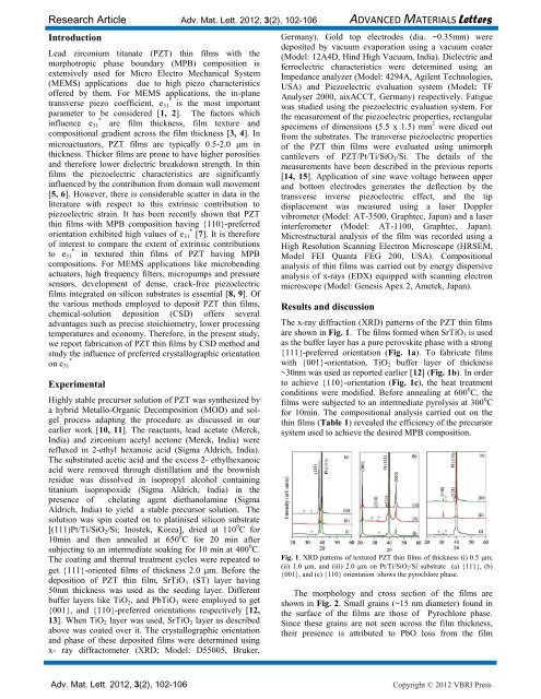
The x-ray diffraction (XRD) patterns <strong>of</strong> the <strong>PZT</strong> <strong>thin</strong> <strong>films</strong><br />
are shown in Fig. 1. The <strong>films</strong> formed when SrTiO3 is used<br />
as the buffer layer has a pure perovskite phase <strong>with</strong> a strong<br />
{111}-preferred orientation (Fig. 1a). To fabricate <strong>films</strong><br />
<strong>with</strong> {001}-orientation, TiO2 buffer layer <strong>of</strong> thickness<br />
~30nm was used as reported earlier [12] (Fig. 1b). In order<br />
to achieve {110}-orientation (Fig. 1c), the heat treatment<br />
conditions were modified. Before annealing at 600 0 C, the<br />
<strong>films</strong> were subjected to an intermediate pyrolysis at 300 0 C<br />
for 10min. The compositional analysis carried out on the<br />
<strong>thin</strong> <strong>films</strong> (Table 1) revealed the efficiency <strong>of</strong> the precursor<br />
system used to achieve the desired MPB composition.<br />
Fig. 1. XRD patterns <strong>of</strong> textured <strong>PZT</strong> <strong>thin</strong> <strong>films</strong> <strong>of</strong> thickness (i) 0.5 m;<br />
(ii) 1.0 m, and (iii) 2.0 m on Pt/Ti/SiO2/Si substrate (a) {111}, (b)<br />
{001}, and (c) {110} orientation :shows the pyrochlore phase.<br />
The morphology and cross section <strong>of</strong> the <strong>films</strong> are<br />
shown in Fig. 2. Small grains (~15 nm diameter) found in<br />
the surface <strong>of</strong> the <strong>films</strong> are those <strong>of</strong> Pyrochlore phase.<br />
Since these grains are not seen across the film thickness,<br />
their presence is attributed to PbO loss from the film<br />
Adv. Mat. Lett. 2012, 3(2), 102-106 Copyright © 2012 VBRI Press