

dsPIC33F/PIC24H Flash Programming Specification - Microchip
dsPIC33F/PIC24H Flash Programming Specification - Microchip
dsPIC33F/PIC24H Flash Programming Specification - Microchip

You also want an ePaper? Increase the reach of your titles
YUMPU automatically turns print PDFs into web optimized ePapers that Google loves.
1.0 DEVICE OVERVIEW<br />
This document defines the programming specification<br />
for the <strong>dsPIC33F</strong> 16-bit Digital Signal Controller (DSC)<br />
and <strong>PIC24H</strong> 16-bit Microcontroller (MCU) families. This<br />
programming specification is required only for those<br />
developing programming support for the <strong>dsPIC33F</strong>/<br />
<strong>PIC24H</strong> family. Customers using only one of these<br />
devices should use development tools that already<br />
provide support for device programming.<br />
Topics covered include:<br />
1.0 Device Overview ......................................................... 1<br />
2.0 <strong>Programming</strong> Overview of the <strong>dsPIC33F</strong>/<strong>PIC24H</strong> ...... 1<br />
3.0 Device <strong>Programming</strong> – Enhanced ICSP ..................... 8<br />
4.0 The <strong>Programming</strong> Executive ..................................... 19<br />
5.0 Device <strong>Programming</strong> – ICSP .................................... 28<br />
6.0 <strong>Programming</strong> the <strong>Programming</strong> Executive<br />
to Memory ................................................................. 45<br />
7.0 Device ID................................................................... 50<br />
8.0 AC/DC Characteristics and Timing Requirements .... 54<br />
Appendix A: Hex File Format .............................................. 57<br />
Appendix B: Device ID Register Silicon Errata Addendum. 58<br />
Appendix C: Diagnostic and Calibration Registers ............. 59<br />
Appendix D: Checksum Computation ................................. 61<br />
Appendix E: Revision History.............................................. 74<br />
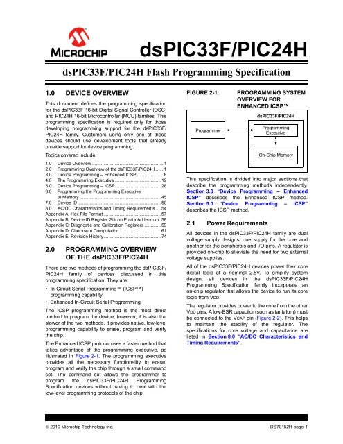
2.0 PROGRAMMING OVERVIEW<br />
OF THE <strong>dsPIC33F</strong>/<strong>PIC24H</strong><br />
There are two methods of programming the <strong>dsPIC33F</strong>/<br />
<strong>PIC24H</strong> family of devices discussed in this<br />
programming specification. They are:<br />
• In-Circuit Serial <strong>Programming</strong> (ICSP)<br />
programming capability<br />
• Enhanced In-Circuit Serial <strong>Programming</strong><br />
The ICSP programming method is the most direct<br />
method to program the device; however, it is also the<br />
slower of the two methods. It provides native, low-level<br />
programming capability to erase, program and verify<br />
the chip.<br />
The Enhanced ICSP protocol uses a faster method that<br />
takes advantage of the programming executive, as<br />
illustrated in Figure 2-1. The programming executive<br />
provides all the necessary functionality to erase,<br />
program and verify the chip through a small command<br />
set. The command set allows the programmer to<br />
program the <strong>dsPIC33F</strong>/<strong>PIC24H</strong> <strong>Programming</strong><br />
<strong>Specification</strong> devices without having to deal with the<br />
low-level programming protocols of the chip.<br />
<strong>dsPIC33F</strong>/<strong>PIC24H</strong><br />
<strong>dsPIC33F</strong>/<strong>PIC24H</strong> <strong>Flash</strong> <strong>Programming</strong> <strong>Specification</strong><br />
FIGURE 2-1: PROGRAMMING SYSTEM<br />
OVERVIEW FOR<br />
ENHANCED ICSP<br />
Programmer<br />
This specification is divided into major sections that<br />
describe the programming methods independently.<br />
Section 3.0 “Device <strong>Programming</strong> – Enhanced<br />
ICSP” describes the Enhanced ICSP method.<br />
Section 5.0 “Device <strong>Programming</strong> – ICSP”<br />
describes the ICSP method.<br />
2.1 Power Requirements<br />
<strong>dsPIC33F</strong>/<strong>PIC24H</strong><br />
<strong>Programming</strong><br />
Executive<br />
On-Chip Memory<br />
All devices in the <strong>dsPIC33F</strong>/<strong>PIC24H</strong> family are dual<br />
voltage supply designs: one supply for the core and<br />
another for the peripherals and I/O pins. A regulator is<br />
provided on-chip to alleviate the need for two external<br />
voltage supplies.<br />
All of the <strong>dsPIC33F</strong>/<strong>PIC24H</strong> devices power their core<br />
digital logic at a nominal 2.5V. To simplify system<br />
design, all devices in the <strong>dsPIC33F</strong>/<strong>PIC24H</strong><br />
<strong>Programming</strong> <strong>Specification</strong> family incorporate an<br />
on-chip regulator that allows the device to run its core<br />
logic from VDD.<br />
The regulator provides power to the core from the other<br />
VDD pins. A low-ESR capacitor (such as tantalum) must<br />
be connected to the VCAP pin (Figure 2-2). This helps<br />
to maintain the stability of the regulator. The<br />
specifications for core voltage and capacitance are<br />
listed in Section 8.0 “AC/DC Characteristics and<br />
Timing Requirements”.<br />
© 2010 <strong>Microchip</strong> Technology Inc. DS70152H-page 1
<strong>dsPIC33F</strong>/<strong>PIC24H</strong> PROGRAMMING SPECIFICATION<br />
FIGURE 2-2: CONNECTIONS FOR THE<br />
ON-CHIP REGULATOR<br />
CEFC<br />
3.3V<br />
VDD<br />
VCAP<br />
VSS<br />
<strong>dsPIC33F</strong>/<strong>PIC24H</strong><br />
Note 1: These are typical operating voltages. Refer<br />
to TABLE 8-1: “AC/DC Characteristics<br />
and Timing Requirements” for the full<br />
operating ranges of VDD and VCAP.<br />
2: It is important for the low-ESR capacitor to<br />
be placed as close as possible to the VCAP<br />
pin.<br />
TABLE 2-1: PINS USED DURING PROGRAMMING<br />
Pin Name<br />
2.2 Program Memory Write/Erase<br />
Requirements<br />
The program <strong>Flash</strong> memory on the <strong>dsPIC33F</strong>/<strong>PIC24H</strong><br />
has a specific write/erase requirement that must be<br />
adhered to, for proper device operation. The rule is that<br />
any given word in memory must not be written without<br />
first erasing the page in which it is located. Thus, the<br />
easiest way to conform to this rule is to write all the data<br />
in a programming block within one write cycle. The<br />
programming methods specified in this document<br />
comply with this requirement.<br />
Note: A program memory word can be<br />
programmed twice before an erase, but<br />
only if (a) the same data is used in both<br />
program operations or (b) bits containing<br />
‘1’ are set to ‘0’ but no ‘0’ is set to ‘1’.<br />
2.3 Pins Used During <strong>Programming</strong><br />
The pins that are used for programming are listed in<br />
Table 2-1.<br />
Note: Refer to the specific device data sheet for<br />
complete pin diagrams of the <strong>dsPIC33F</strong>/<br />
<strong>PIC24H</strong> devices.<br />
During <strong>Programming</strong><br />
Pin Name Pin Type Pin Description<br />
MCLR MCLR P <strong>Programming</strong> Enable<br />
VDD and AVDD (1)<br />
VDD P Power Supply<br />
VSS and AVSS (1)<br />
VSS P Ground<br />
VCAP VCAP P CPU Logic Filter Capacitor Connection<br />
PGEC1 PGEC1 I Primary <strong>Programming</strong> Pin Pair: Serial Clock<br />
PGED1 PGED1 I/O Primary <strong>Programming</strong> Pin Pair: Serial Data<br />
PGEC2 PGEC2 I Secondary <strong>Programming</strong> Pin Pair: Serial Clock<br />
PGED2 PGED2 I/O Secondary <strong>Programming</strong> Pin Pair: Serial Data<br />
PGEC3 PGEC3 I Tertiary <strong>Programming</strong> Pin Pair: Serial Clock<br />
PGED3 PGED3 I/O Tertiary <strong>Programming</strong> Pin Pair: Serial Data<br />
Legend: I = Input O = Output P = Power<br />
Note 1: All power supply and ground pins must be connected, including analog supplies (AVDD) and ground<br />
(AVSS).<br />
DS70152H-page 2 © 2010 <strong>Microchip</strong> Technology Inc.
<strong>dsPIC33F</strong>/<strong>PIC24H</strong> PROGRAMMING SPECIFICATION<br />
2.4 Memory Map<br />
The program memory map extends from 0x0 to<br />
0xFFFFFE. Code storage is located at the base of the<br />
memory map and supports up to 88K instructions<br />
(about 256 Kbytes). Table 2-2 shows the program<br />
memory size and number of erase and program blocks<br />
present in each device variant. Each erase block or<br />
page contains 512 instructions and each program block<br />
or row, contains 64 instructions.<br />
Locations 0x800000 through 0x800FFE are reserved<br />
for executive code memory. This region stores the<br />
programming executive and the debugging<br />
executive. The programming executive is used for<br />
TABLE 2-2: CODE MEMORY SIZE<br />
<strong>dsPIC33F</strong>/<strong>PIC24H</strong> Device<br />
User Memory Address<br />
Limit<br />
(Instruction Words)<br />
device programming and the debug executive is<br />
used for in-circuit debugging. This region of memory<br />
cannot be used to store user code.<br />
Locations 0xF80000 through 0xF80017 are reserved<br />
for the device Configuration registers.<br />
Locations 0xFF0000 and 0xFF0002 are reserved for<br />
the Device ID Word registers. These bits can be used<br />
by the programmer to identify which device type is<br />
being programmed. They are described in Section 7.0<br />
“Device ID”. The Device ID registers read out<br />
normally, even after code protection is applied.<br />
Figure 2-3 illustrates the memory map for the<br />
<strong>dsPIC33F</strong>/<strong>PIC24H</strong> family variants.<br />
Write Blocks Erase Blocks<br />
Executive Memory<br />
Address Limit<br />
(Instruction Words)<br />
<strong>dsPIC33F</strong>J06GS101 0x000FFE (2K) 32 4 0x8007FE (1K)<br />
<strong>dsPIC33F</strong>J06GS102 0x000FFE (2K) 32 4 0x8007FE (1K)<br />
<strong>dsPIC33F</strong>J06GS202 0x000FFE (2K) 32 4 0x8007FE (1K)<br />
<strong>dsPIC33F</strong>J16GS402 0x002BFE (6K) 88 11 0x8007FE (1K)<br />
<strong>dsPIC33F</strong>J16GS404 0x002BFE (6K) 88 11 0x8007FE (1K)<br />
<strong>dsPIC33F</strong>J16GS502 0x002BFE (6K) 88 11 0x8007FE (1K)<br />
<strong>dsPIC33F</strong>J16GS504 0x002BFE (6K) 88 11 0x8007FE (1K)<br />
<strong>dsPIC33F</strong>J12GP201 0x001FFE (4K) 64 8 0x8007FE (1K)<br />
<strong>dsPIC33F</strong>J12GP202 0x001FFE (4K) 64 8 0x8007FE (1K)<br />
<strong>dsPIC33F</strong>J16GP304 0x002BFE (6K) 88 11 0x800FFE (2K)<br />
<strong>dsPIC33F</strong>J32GP202 0x0057FE (11K) 176 22 0x800FFE (2K)<br />
<strong>dsPIC33F</strong>J32GP204 0x0057FE (11K) 176 22 0x800FFE (2K)<br />
<strong>dsPIC33F</strong>J32GP302 0x0057FE (11K) 176 22 0x800FFE (2K)<br />
<strong>dsPIC33F</strong>J32GP304 0x0057FE (11K) 176 22 0x800FFE (2K)<br />
<strong>dsPIC33F</strong>J64GP202 0x00ABFE (22K) 344 43 0x800FFE (2K)<br />
<strong>dsPIC33F</strong>J64GP204 0x00ABFE (22K) 344 43 0x800FFE (2K)<br />
<strong>dsPIC33F</strong>J64GP206 0x00ABFE (22K) 344 43 0x800FFE (2K)<br />
<strong>dsPIC33F</strong>J64GP306 0x00ABFE (22K) 344 43 0x800FFE (2K)<br />
<strong>dsPIC33F</strong>J64GP310 0x00ABFE (22K) 344 43 0x800FFE (2K)<br />
<strong>dsPIC33F</strong>J64GP706 0x00ABFE (22K) 344 43 0x800FFE (2K)<br />
<strong>dsPIC33F</strong>J64GP708 0x00ABFE (22K) 344 43 0x800FFE (2K)<br />
<strong>dsPIC33F</strong>J64GP710 0x00ABFE (22K) 344 43 0x800FFE (2K)<br />
<strong>dsPIC33F</strong>J64GP802 0x00ABFE (22K) 344 43 0x800FFE (2K)<br />
<strong>dsPIC33F</strong>J64GP804 0x00ABFE (22K) 344 43 0x800FFE (2K)<br />
<strong>dsPIC33F</strong>J128GP202 0x0157FE (44K) 688 86 0x800FFE (2K)<br />
<strong>dsPIC33F</strong>J128GP204 0x0157FE (44K) 688 86 0x800FFE (2K)<br />
<strong>dsPIC33F</strong>J128GP206 0x0157FE (44K) 688 86 0x800FFE (2K)<br />
<strong>dsPIC33F</strong>J128GP306 0x0157FE (44K) 688 86 0x800FFE (2K)<br />
<strong>dsPIC33F</strong>J128GP310 0x0157FE (44K) 688 86 0x800FFE (2K)<br />
<strong>dsPIC33F</strong>J128GP706 0x0157FE (44K) 688 86 0x800FFE (2K)<br />
<strong>dsPIC33F</strong>J128GP708 0x0157FE (44K) 688 86 0x800FFE (2K)<br />
© 2010 <strong>Microchip</strong> Technology Inc. DS70152H-page 3
<strong>dsPIC33F</strong>/<strong>PIC24H</strong> PROGRAMMING SPECIFICATION<br />
TABLE 2-2: CODE MEMORY SIZE (CONTINUED)<br />
<strong>dsPIC33F</strong>/<strong>PIC24H</strong> Device<br />
User Memory Address<br />
Limit<br />
(Instruction Words)<br />
Write Blocks Erase Blocks<br />
Executive Memory<br />
Address Limit<br />
(Instruction Words)<br />
<strong>dsPIC33F</strong>J128GP710 0x0157FE (44K) 688 86 0x800FFE (2K)<br />
<strong>dsPIC33F</strong>J128GP802 0x0157FE (44K) 688 86 0x800FFE (2K)<br />
<strong>dsPIC33F</strong>J128GP804 0x0157FE (44K) 688 86 0x800FFE (2K)<br />
<strong>dsPIC33F</strong>J256GP506 0x02ABFE (88K) 1368 171 0x800FFE (2K)<br />
<strong>dsPIC33F</strong>J256GP510 0x02ABFE (88K) 1368 171 0x800FFE (2K)<br />
<strong>dsPIC33F</strong>J256GP710 0x02ABFE (88K) 1368 171 0x800FFE (2K)<br />
<strong>dsPIC33F</strong>J12MC201 0x001FFE (4K) 64 8 0x8007FE (1K)<br />
<strong>dsPIC33F</strong>J12MC202 0x001FFE (4K) 64 8 0x8007FE (1K)<br />
<strong>dsPIC33F</strong>J16MC304 0x002BFE (6K) 88 11 0x800FFE (2K)<br />
<strong>dsPIC33F</strong>J32MC202 0x0057FE (11K) 176 22 0x800FFE (2K)<br />
<strong>dsPIC33F</strong>J32MC204 0x0057FE (11K) 176 22 0x800FFE (2K)<br />
<strong>dsPIC33F</strong>J32MC302 0x0057FE (11K) 176 22 0x800FFE (2K)<br />
<strong>dsPIC33F</strong>J32MC304 0x0057FE (11K) 176 22 0x800FFE (2K)<br />
<strong>dsPIC33F</strong>J64MC202 0x00ABFE (22K) 344 43 0x800FFE (2K)<br />
<strong>dsPIC33F</strong>J64MC204 0x00ABFE (22K) 344 43 0x800FFE (2K)<br />
<strong>dsPIC33F</strong>J64MC506 0x00ABFE (22K) 344 43 0x800FFE (2K)<br />
<strong>dsPIC33F</strong>J64MC508 0x00ABFE (22K) 344 43 0x800FFE (2K)<br />
<strong>dsPIC33F</strong>J64MC510 0x00ABFE (22K) 344 43 0x800FFE (2K)<br />
<strong>dsPIC33F</strong>J64MC706 0x00ABFE (22K) 344 43 0x800FFE (2K)<br />
<strong>dsPIC33F</strong>J64MC710 0x00ABFE (22K) 344 43 0x800FFE (2K)<br />
<strong>dsPIC33F</strong>J64MC802 0x00ABFE (22K) 344 43 0x800FFE (2K)<br />
<strong>dsPIC33F</strong>J64MC804 0x00ABFE (22K) 344 43 0x800FFE (2K)<br />
<strong>dsPIC33F</strong>J128MC202 0x0157FE (44K) 688 86 0x800FFE (2K)<br />
<strong>dsPIC33F</strong>J128MC204 0x0157FE (44K) 688 86 0x800FFE (2K)<br />
<strong>dsPIC33F</strong>J128MC506 0x0157FE (44K) 688 86 0x800FFE (2K)<br />
<strong>dsPIC33F</strong>J128MC510 0x0157FE (44K) 688 86 0x800FFE (2K)<br />
<strong>dsPIC33F</strong>J128MC706 0x0157FE (44K) 688 86 0x800FFE (2K)<br />
<strong>dsPIC33F</strong>J128MC708 0x0157FE (44K) 688 86 0x800FFE (2K)<br />
<strong>dsPIC33F</strong>J128MC710 0x0157FE (44K) 688 86 0x800FFE (2K)<br />
<strong>dsPIC33F</strong>J128MC802 0x0157FE (44K) 688 86 0x800FFE (2K)<br />
<strong>dsPIC33F</strong>J128MC804 0x0157FE (44K) 688 86 0x800FFE (2K)<br />
<strong>dsPIC33F</strong>J256MC510 0x02ABFE (88K) 1368 171 0x800FFE (2K)<br />
<strong>dsPIC33F</strong>J256MC710 0x02ABFE (88K) 1368 171 0x800FFE (2K)<br />
<strong>PIC24H</strong>J12GP201 0x001FFE (4K) 64 8 0x8007FE (1K)<br />
<strong>PIC24H</strong>J12GP202 0x001FFE (4K) 64 8 0x8007FE (1K)<br />
<strong>PIC24H</strong>J16GP304 0x002BFE (6K) 88 11 0x800FFE (2K)<br />
<strong>PIC24H</strong>J32GP202 0x0057FE (11K) 176 22 0x800FFE (2K)<br />
<strong>PIC24H</strong>J32GP204 0x0057FE (11K) 176 22 0x800FFE (2K)<br />
<strong>PIC24H</strong>J32GP302 0x0057FE (11K) 176 22 0x800FFE (2K)<br />
<strong>PIC24H</strong>J32GP304 0x0057FE (11K) 176 22 0x800FFE (2K)<br />
<strong>PIC24H</strong>J64GP202 0x00ABFE (22K) 344 43 0x800FFE (2K)<br />
<strong>PIC24H</strong>J64GP204 0x00ABFE (22K) 344 43 0x800FFE (2K)<br />
<strong>PIC24H</strong>J64GP206 0x00ABFE (22K) 344 43 0x800FFE (2K)<br />
DS70152H-page 4 © 2010 <strong>Microchip</strong> Technology Inc.
<strong>dsPIC33F</strong>/<strong>PIC24H</strong> PROGRAMMING SPECIFICATION<br />
TABLE 2-2: CODE MEMORY SIZE (CONTINUED)<br />
<strong>dsPIC33F</strong>/<strong>PIC24H</strong> Device<br />
User Memory Address<br />
Limit<br />
(Instruction Words)<br />
Write Blocks Erase Blocks<br />
Executive Memory<br />
Address Limit<br />
(Instruction Words)<br />
<strong>PIC24H</strong>J64GP210 0x00ABFE (22K) 344 43 0x800FFE (2K)<br />
<strong>PIC24H</strong>J64GP502 0x00ABFE (22K) 344 43 0x800FFE (2K)<br />
<strong>PIC24H</strong>J64GP504 0x00ABFE (22K) 344 43 0x800FFE (2K)<br />
<strong>PIC24H</strong>J64GP506 0x00ABFE (22K) 344 43 0x800FFE (2K)<br />
<strong>PIC24H</strong>J64GP510 0x00ABFE (22K) 344 43 0x800FFE (2K)<br />
<strong>PIC24H</strong>J128GP202 0x0157FE (44K) 688 86 0x800FFE (2K)<br />
<strong>PIC24H</strong>J128GP204 0x0157FE (44K) 688 86 0x800FFE (2K)<br />
<strong>PIC24H</strong>J128GP206 0x0157FE (44K) 688 86 0x800FFE (2K)<br />
<strong>PIC24H</strong>J128GP210 0x0157FE (44K) 688 86 0x800FFE (2K)<br />
<strong>PIC24H</strong>J128GP306 0x0157FE (44K) 688 86 0x800FFE (2K)<br />
<strong>PIC24H</strong>J128GP310 0x0157FE (44K) 688 86 0x800FFE (2K)<br />
<strong>PIC24H</strong>J128GP502 0x0157FE (44K) 688 86 0x800FFE (2K)<br />
<strong>PIC24H</strong>J128GP504 0x0157FE (44K) 688 86 0x800FFE (2K)<br />
<strong>PIC24H</strong>J128GP506 0x0157FE (44K) 688 86 0x800FFE (2K)<br />
<strong>PIC24H</strong>J128GP510 0x0157FE (44K) 688 86 0x800FFE (2K)<br />
<strong>PIC24H</strong>J256GP206 0x02ABFE (88K) 1368 171 0x800FFE (2K)<br />
<strong>PIC24H</strong>J256GP210 0x02ABFE (88K) 1368 171 0x800FFE (2K)<br />
<strong>PIC24H</strong>J256GP610 0x02ABFE (88K) 1368 171 0x800FFE (2K)<br />
<strong>dsPIC33F</strong>J64GP206A 0x00ABFE (22K) 344 43 0x800FFE (2k)<br />
<strong>dsPIC33F</strong>J64GP306A 0x00ABFE (22K) 344 43 0x800FFE (2k)<br />
<strong>dsPIC33F</strong>J64GP310A 0x00ABFE (22K) 344 43 0x800FFE (2k)<br />
<strong>dsPIC33F</strong>J64GP706A 0x00ABFE (22K) 344 43 0x800FFE (2k)<br />
<strong>dsPIC33F</strong>J64GP708A 0x00ABFE (22K) 344 43 0x800FFE (2k)<br />
<strong>dsPIC33F</strong>J64GP710A 0x00ABFE (22K) 344 43 0x800FFE (2k)<br />
<strong>dsPIC33F</strong>J64MC506A 0x00ABFE (22K) 344 43 0x800FFE (2k)<br />
<strong>dsPIC33F</strong>J64MC508A 0x00ABFE (22K) 344 43 0x800FFE (2k)<br />
<strong>dsPIC33F</strong>J64MC510A 0x00ABFE (22K) 344 43 0x800FFE (2k)<br />
<strong>dsPIC33F</strong>J64MC706A 0x00ABFE (22K) 344 43 0x800FFE (2k)<br />
<strong>dsPIC33F</strong>J64MC710A 0x00ABFE (22K) 344 43 0x800FFE (2k)<br />
<strong>PIC24H</strong>J64GP206A 0x00ABFE (22K) 344 43 0x800FFE (2k)<br />
<strong>PIC24H</strong>J64GP210A 0x00ABFE (22K) 344 43 0x800FFE (2k)<br />
<strong>PIC24H</strong>J64GP506A 0x00ABFE (22K) 344 43 0x800FFE (2k)<br />
<strong>PIC24H</strong>J64GP510A 0x00ABFE (22K) 344 43 0x800FFE (2k)<br />
<strong>dsPIC33F</strong>J128GP206A 0x0157FE (44K) 688 86 0x800FFE (2k)<br />
<strong>dsPIC33F</strong>J128GP306A 0x0157FE (44K) 688 86 0x800FFE (2k)<br />
<strong>dsPIC33F</strong>J128GP310A 0x0157FE (44K) 688 86 0x800FFE (2k)<br />
<strong>dsPIC33F</strong>J128GP706A 0x0157FE (44K) 688 86 0x800FFE (2k)<br />
<strong>dsPIC33F</strong>J128GP708A 0x0157FE (44K) 688 86 0x800FFE (2k)<br />
<strong>dsPIC33F</strong>J128GP710A 0x0157FE (44K) 688 86 0x800FFE (2k)<br />
<strong>dsPIC33F</strong>J128MC506A 0x0157FE (44K) 688 86 0x800FFE (2k)<br />
<strong>dsPIC33F</strong>J128MC510A 0x0157FE (44K) 688 86 0x800FFE (2k)<br />
<strong>dsPIC33F</strong>J128MC706A 0x0157FE (44K) 688 86 0x800FFE (2k)<br />
<strong>dsPIC33F</strong>J128MC708A 0x0157FE (44K) 688 86 0x800FFE (2k)<br />
© 2010 <strong>Microchip</strong> Technology Inc. DS70152H-page 5
<strong>dsPIC33F</strong>/<strong>PIC24H</strong> PROGRAMMING SPECIFICATION<br />
TABLE 2-2: CODE MEMORY SIZE (CONTINUED)<br />
<strong>dsPIC33F</strong>/<strong>PIC24H</strong> Device<br />
User Memory Address<br />
Limit<br />
(Instruction Words)<br />
Write Blocks Erase Blocks<br />
Executive Memory<br />
Address Limit<br />
(Instruction Words)<br />
<strong>dsPIC33F</strong>J128MC710A 0x0157FE (44K) 688 86 0x800FFE (2k)<br />
<strong>PIC24H</strong>J128GP206A 0x0157FE (44K) 688 86 0x800FFE (2k)<br />
<strong>PIC24H</strong>J128GP210A 0x0157FE (44K) 688 86 0x800FFE (2k)<br />
<strong>PIC24H</strong>J128GP306A 0x0157FE (44K) 688 86 0x800FFE (2k)<br />
<strong>PIC24H</strong>J128GP310A 0x0157FE (44K) 688 86 0x800FFE (2k)<br />
<strong>PIC24H</strong>J128GP506A 0x0157FE (44K) 688 86 0x800FFE (2k)<br />
<strong>PIC24H</strong>J128GP510A 0x0157FE (44K) 688 86 0x800FFE (2k)<br />
<strong>dsPIC33F</strong>J256GP506A 0x02ABFE (88K) 1368 171 0x800FFE (2k)<br />
<strong>dsPIC33F</strong>J256GP510A 0x02ABFE (88K) 1368 171 0x800FFE (2k)<br />
<strong>dsPIC33F</strong>J256GP710A 0x02ABFE (88K) 1368 171 0x800FFE (2k)<br />
<strong>dsPIC33F</strong>J256MC510A 0x02ABFE (88K) 1368 171 0x800FFE (2k)<br />
<strong>dsPIC33F</strong>J256MC710A 0x02ABFE (88K) 1368 171 0x800FFE (2k)<br />
<strong>PIC24H</strong>J256GP206A 0x02ABFE (88K) 1368 171 0x800FFE (2k)<br />
<strong>PIC24H</strong>J256GP210A 0x02ABFE (88K) 1368 171 0x800FFE (2k)<br />
<strong>PIC24H</strong>J256GP610A 0x02ABFE (88K) 1368 171 0x800FFE (2k)<br />
<strong>dsPIC33F</strong>J32GS406 0x0057FE (11K) 176 22 0x800FFE (2k)<br />
<strong>dsPIC33F</strong>J32GS606 0x0057FE (11K) 176 22 0x800FFE (2k)<br />
<strong>dsPIC33F</strong>J32GS608 0x0057FE (11K) 176 22 0x800FFE (2k)<br />
<strong>dsPIC33F</strong>J32GS610 0x0057FE (11K) 176 22 0x800FFE (2k)<br />
<strong>dsPIC33F</strong>J64GS406 0x00ABFE (22K) 344 43 0x800FFE (2k)<br />
<strong>dsPIC33F</strong>J64GS606 0x00ABFE (22K) 344 43 0x800FFE (2k)<br />
<strong>dsPIC33F</strong>J64GS608 0x00ABFE (22K) 344 43 0x800FFE (2k)<br />
<strong>dsPIC33F</strong>J64GS610 0x00ABFE (22K) 344 43 0x800FFE (2k)<br />
DS70152H-page 6 © 2010 <strong>Microchip</strong> Technology Inc.
<strong>dsPIC33F</strong>/<strong>PIC24H</strong> PROGRAMMING SPECIFICATION<br />
FIGURE 2-3: PROGRAM MEMORY MAP<br />
User Memory<br />
Space<br />
Configuration Memory<br />
Space<br />
User <strong>Flash</strong><br />
Code Memory<br />
(87552 x 24-bit)<br />
Reserved<br />
Executive Code Memory<br />
(2048 x 24-bit)<br />
Reserved<br />
0x000000<br />
0x02ABFE<br />
0x02AC00<br />
0x7FFFFE<br />
0x800000<br />
0xF7FFFE<br />
Configuration Registers 0xF80000<br />
(12 x 8-bit) 0xF80016<br />
0xF80018<br />
Reserved<br />
Device ID<br />
(2 x 16-bit)<br />
Reserved<br />
0x800FFE<br />
0x801000<br />
0xFEFFFE<br />
0xFF0000<br />
0xFF0002<br />
0xFF0004<br />
0xFFFFFE<br />
Note: The address boundaries for user <strong>Flash</strong> and Executive code memory are device dependent.<br />
© 2010 <strong>Microchip</strong> Technology Inc. DS70152H-page 7
<strong>dsPIC33F</strong>/<strong>PIC24H</strong> PROGRAMMING SPECIFICATION<br />
3.0 DEVICE PROGRAMMING –<br />
ENHANCED ICSP<br />
This section discusses programming the device<br />
through Enhanced ICSP and the programming<br />
executive. The programming executive resides in<br />
executive memory (separate from code memory) and is<br />
executed when Enhanced ICSP <strong>Programming</strong> mode is<br />
entered. The programming executive provides the<br />
mechanism for the programmer (host device) to<br />
program and verify the <strong>dsPIC33F</strong>/<strong>PIC24H</strong><br />
<strong>Programming</strong> <strong>Specification</strong> family devices using a<br />
simple command set and communication protocol.<br />
There are several basic functions provided by the<br />
programming executive:<br />
• Read Memory<br />
• Erase Memory<br />
• Program Memory<br />
• Blank Check<br />
• Read Executive Firmware Revision<br />
The programming executive performs the low-level<br />
tasks required for erasing, programming and verifying<br />
a device. This allows the programmer to program the<br />
device by issuing the appropriate commands and data.<br />
Table 3-1 summarizes the commands. A detailed<br />
description for each command is provided in<br />
Section 4.2 “<strong>Programming</strong> Executive Commands”.<br />
TABLE 3-1: COMMAND SET SUMMARY<br />
Command Description<br />
SCHECK Sanity check.<br />
READC Read Configuration registers or<br />
Device ID registers.<br />
READP Read code memory.<br />
PROGC Program a Configuration<br />
register and verify.<br />
PROGP Program one row of code<br />
memory and verify.<br />
ERASEP Erase Page command.<br />
CRCP SIGNATURE Performs CRC on memory.<br />
QBLANK Query to check whether code<br />
memory is blank.<br />
QVER Query the software version.<br />
The programming executive uses the device’s data<br />
RAM for variable storage and program execution. After<br />
the programming executive is run, no assumptions<br />
should be made about the contents of data RAM.<br />
3.1 Overview of the <strong>Programming</strong><br />
Process<br />
Figure 3-1 illustrates the high-level overview of the<br />
programming process. After entering Enhanced ICSP<br />
mode, the programming executive is verified. Next, the<br />
device is erased. Then, the code memory is<br />
programmed, followed by the nonvolatile device<br />
Configuration registers. Code memory (including the<br />
Configuration registers) is then verified to ensure that<br />
programming was successful.<br />
After the programming executive has been verified<br />
in memory (or loaded if not present), the <strong>dsPIC33F</strong>/<br />
<strong>PIC24H</strong> <strong>Programming</strong> <strong>Specification</strong> can be<br />
programmed using the command set shown in<br />
Table 3-1.<br />
FIGURE 3-1: HIGH-LEVEL ENHANCED<br />
ICSP PROGRAMMING<br />
FLOW<br />
DS70152H-page 8 © 2010 <strong>Microchip</strong> Technology Inc.<br />
Start<br />
Perform Bulk Erase<br />
(using ICSP)<br />
Program PE Into<br />
Executive Memory<br />
(using ICSP)<br />
Enter Enhanced ICSP<br />
Program Memory<br />
Verify Program<br />
Program Configuration Bits<br />
Verify Configuration Bits<br />
Exit Enhanced ICSP<br />
End
<strong>dsPIC33F</strong>/<strong>PIC24H</strong> PROGRAMMING SPECIFICATION<br />
3.2 Confirming the Presence of the<br />
<strong>Programming</strong> Executive<br />
Before programming, the programmer must confirm<br />
that the programming executive is stored in executive<br />
memory. The procedure for this task is illustrated in<br />
Figure 3-2.<br />
First, ICSP mode is entered. Then, the unique<br />
Application ID Word stored in executive memory is read.<br />
If the programming executive is resident, the correct<br />
Application ID Word is read and programming can<br />
resume as normal. However, if the Application ID Word is<br />
not present, the programming executive must be<br />
programmed to executive code memory using the<br />
method described in Section 6.0 “<strong>Programming</strong> the<br />
<strong>Programming</strong> Executive to Memory”. See Table 7-1<br />
for the Application ID of each device.<br />
Section 5.0 “Device <strong>Programming</strong> – ICSP” describes<br />
the ICSP programming method. Section 5.11 “Reading<br />
the Application ID Word” describes the procedure for<br />
reading the Application ID Word in ICSP mode.<br />
FIGURE 3-2: CONFIRMING PRESENCE<br />
OF PROGRAMMING<br />
EXECUTIVE<br />
Start<br />
Enter ICSP Mode<br />
Check the<br />
Application ID<br />
by reading Address<br />
0x8007F0<br />
Is<br />
Application ID<br />
present? (1)<br />
Yes<br />
Exit ICSP Mode<br />
Enter Enhanced<br />
ICSP Mode<br />
Sanity Check<br />
End<br />
No<br />
Prog. Executive must<br />
be Programmed<br />
Note 1: See TABLE 7-1: “Device IDs and Revision”<br />
for the Application ID of each<br />
device.<br />
3.3 Entering Enhanced ICSP Mode<br />
As illustrated in Figure 3-3, entering Enhanced ICSP<br />
Program/Verify mode requires three steps:<br />
1. The MCLR pin is briefly driven high then low.<br />
2. A 32-bit key sequence is clocked into PGDx.<br />
3. MCLR is then driven high within a specified<br />
period of time and held.<br />
The programming voltage applied to MCLR is VIH,<br />
which is essentially VDD in case of <strong>dsPIC33F</strong>/<strong>PIC24H</strong><br />
devices. There is no minimum time requirement for<br />
holding at VIH. After VIH is removed, an interval of at<br />
least P18 must elapse before presenting the key<br />
sequence on PGDx.<br />
The key sequence is a specific 32-bit pattern,<br />
‘0100 1101 0100 0011 0100 1000 0101 0000’<br />
(more easily remembered as 0x4D434850 in<br />
hexadecimal format). The device will enter Program/<br />
Verify mode only if the key sequence is valid. The Most<br />
Significant bit (MSb) of the most significant nibble must<br />
be shifted in first.<br />
Once the key sequence is complete, VIH must be<br />
applied to MCLR and held at that level for as long as<br />
Program/Verify mode is to be maintained. An interval<br />
time of at least P19 and P7 must elapse before<br />
presenting data on PGDx. Signals appearing on PGDx<br />
before P7 has elapsed will not be interpreted as valid.<br />
On successful entry, the program memory can be<br />
accessed and programmed in serial fashion. While in<br />
the Program/Verify mode, all unused I/Os are placed in<br />
the high-impedance state.<br />
Note: When programming a device without<br />
Peripheral Pin Select (PPS) and in<br />
Enhanced ICSP mode, the SPI output pin<br />
(SDOx) may toggle while the device is<br />
being programmed.<br />
© 2010 <strong>Microchip</strong> Technology Inc. DS70152H-page 9
<strong>dsPIC33F</strong>/<strong>PIC24H</strong> PROGRAMMING SPECIFICATION<br />
FIGURE 3-3: ENTERING ENHANCED ICSP MODE<br />
MCLR<br />
VDD<br />
PGDx<br />
PGCx<br />
P6<br />
3.4 Blank Check<br />
P14<br />
P18<br />
VIH<br />
The term “Blank Check” implies verifying that the<br />
device has been successfully erased and has no<br />
programmed memory locations. A blank or erased<br />
memory location is always read as ‘1’.<br />
The Device ID registers (0xFF0000:0xFF0002) can be<br />
ignored by the Blank Check since this region stores<br />
device information that cannot be erased. The device<br />
Configuration registers are also ignored by the Blank<br />
Check. Additionally, all unimplemented memory space<br />
should be ignored from the Blank Check.<br />
The QBLANK command is used for the Blank Check. It<br />
determines if the code memory is erased by testing<br />
these memory regions. A ‘BLANK’ or ‘NOT BLANK’<br />
response is returned. If it is determined that the device<br />
is not blank, it must be erased before attempting to<br />
program the chip.<br />
Program/Verify Entry Code = 0x4D434850<br />
0 1 0 0 1 ... 0 0 0 0<br />
b31 b30 b29 b28 b27 b3 b2 b1 b0<br />
P1A<br />
P1B<br />
3.5 Code Memory <strong>Programming</strong><br />
3.5.1 PROGRAMMING METHODOLOGY<br />
Code memory is programmed with the PROGP<br />
command. PROGP programs one row of code memory<br />
starting from the memory address specified in the<br />
command. The number of PROGP commands required<br />
to program a device depends on the number of write<br />
blocks that must be programmed in the device.<br />
A flowchart for programming code memory is illustrated<br />
in Figure 3-4. In this example, all 88K instruction words<br />
of a <strong>dsPIC33F</strong>/<strong>PIC24H</strong> device are programmed. First,<br />
the number of commands to send (called<br />
‘RemainingCmds’ in the flowchart) is set to 1368 and<br />
the destination address (called ‘BaseAddress’) is set to<br />
‘0’. Next, one write block in the device is programmed<br />
with a PROGP command. Each PROGP command<br />
contains data for one row of code memory of the<br />
<strong>dsPIC33F</strong>/<strong>PIC24H</strong>. After the first command is<br />
processed successfully, ‘RemainingCmds’ is<br />
decremented by ‘1’ and compared with ‘0’. Since there<br />
are more PROGP commands to send, ‘BaseAddress’ is<br />
incremented by 0x80 to point to the next row of<br />
memory.<br />
On the second PROGP command, the second row is<br />
programmed. This process is repeated until the entire<br />
device is programmed.<br />
DS70152H-page 10 © 2010 <strong>Microchip</strong> Technology Inc.<br />
VIH<br />
P19<br />
Note: If a bootloader needs to be programmed,<br />
the bootloader code must not be<br />
programmed into the first page of code<br />
memory. For example, if a bootloader<br />
located at address 0x200 attempts to<br />
erase the first page, it would inadvertently<br />
erase itself. Instead, program the<br />
bootloader into the second page (e.g.,<br />
0x400).<br />
P7
<strong>dsPIC33F</strong>/<strong>PIC24H</strong> PROGRAMMING SPECIFICATION<br />
FIGURE 3-4: FLOWCHART FOR<br />
PROGRAMMING CODE<br />
MEMORY<br />
BaseAddress =<br />
BaseAddress + 0x80<br />
No<br />
Start<br />
BaseAddress = 0x0<br />
RemainingCmds = 1368<br />
Send PROGP<br />
Command to Program<br />
BaseAddress<br />
Is<br />
PROGP response<br />
PASS?<br />
End<br />
Yes<br />
RemainingCmds =<br />
RemainingCmds – 1<br />
Is<br />
RemainingCmds<br />
‘0’?<br />
Yes<br />
No<br />
Failure<br />
Report Error<br />
3.5.2 PROGRAMMING VERIFICATION<br />
After code memory is programmed, the contents of<br />
memory can be verified to ensure that programming<br />
was successful. Verification requires code memory to<br />
be read back and compared against the copy held in<br />
the programmer’s buffer.<br />
The READP command can be used to read back all the<br />
programmed code memory.<br />
Alternatively, you can have the programmer perform<br />
the verification after the entire device is programmed,<br />
using a checksum computation.<br />
3.5.3 CHECKSUM COMPUTATION<br />
Only the Configuration registers are included in the<br />
checksum computation. The Device ID and Unit ID are<br />
not included in the checksum computation.<br />
TABLE D-1: “CHECKSUM COMPUTATION” shows<br />
how this 16-bit computation can be made for each<br />
<strong>dsPIC33F</strong> and <strong>PIC24H</strong> device. Computations for read<br />
code protection are shown both enabled and disabled.<br />
The checksum values shown here assume that the<br />
Configuration registers are also erased. However,<br />
when code protection is enabled, the value of the FGS<br />
register is assumed to be 0x5.<br />
© 2010 <strong>Microchip</strong> Technology Inc. DS70152H-page 11
<strong>dsPIC33F</strong>/<strong>PIC24H</strong> PROGRAMMING SPECIFICATION<br />
3.6 Configuration Bits <strong>Programming</strong><br />
3.6.1 OVERVIEW<br />
The <strong>dsPIC33F</strong>/<strong>PIC24H</strong> devices have Configuration<br />
bits stored in twelve 8-bit Configuration registers,<br />
aligned on even configuration memory address<br />
boundaries. These bits can be set or cleared to select<br />
various device configurations. There are three types of<br />
Configuration bits: system operation bits, code-protect<br />
bits and unit ID bits. The system operation bits<br />
determine the power-on settings for system level<br />
TABLE 3-2: <strong>dsPIC33F</strong>/<strong>PIC24H</strong> CONFIGURATION BITS DESCRIPTION<br />
components, such as oscillator and Watchdog Timer.<br />
The code-protect bits prevent program memory from<br />
being read and written.<br />
The register descriptions for the FBS, FSS, FGS,<br />
FOSCSEL, FOSC, FWDT, FPOR and FICD<br />
Configuration registers are shown in Table 3-2.<br />
Note 1: If any of the code-protect bits in FBS,<br />
FSS or FGS is clear, the entire device<br />
must be erased before it can be<br />
reprogrammed.<br />
Bit Field Register Description<br />
RBS FBS Boot Segment Data RAM Code Protection<br />
11 = No RAM is reserved for Boot Segment<br />
10 = Small-Sized Boot RAM<br />
[128 bytes of RAM are reserved for Boot Segment]<br />
01 = Medium-Sized Boot RAM<br />
[256 bytes of RAM are reserved for Boot Segment]<br />
00 = Large-Sized Boot RAM<br />
[1024 bytes of RAM are reserved for Boot Segment]<br />
BSS FBS Boot Segment Program Memory Code Protection<br />
111 = No Boot Segment<br />
110 = Standard security, Small-sized Boot Program <strong>Flash</strong><br />
[Boot Segment ends at 0x0003FF in <strong>dsPIC33F</strong>J06GS101/102/202,<br />
<strong>dsPIC33F</strong>J16GS402/404/502/504, <strong>dsPIC33F</strong>J12GP201/202,<br />
<strong>dsPIC33F</strong>J12MC201/202 and <strong>PIC24H</strong>J12GP201/202.<br />
Boot Segment ends at 0x0007FF in other all other devices.]<br />
101 = Standard security, Medium-sized Boot Program <strong>Flash</strong><br />
[Boot Segment ends at 0x0007FF in <strong>dsPIC33F</strong>J06GS101/102/202,<br />
<strong>dsPIC33F</strong>J16GS402/404/502/504, <strong>dsPIC33F</strong>J12GP201/202,<br />
<strong>dsPIC33F</strong>J12MC201/202 and <strong>PIC24H</strong>J12GP201/202.<br />
Boot Segment ends at 0x001FFF in all other devices.]<br />
100 = Standard security, Large-sized Boot Program <strong>Flash</strong><br />
[Boot Segment ends at 0x000FFF in <strong>dsPIC33F</strong>J06GS101/102/202,<br />
<strong>dsPIC33F</strong>J16GS402/404/502/504, <strong>dsPIC33F</strong>J12GP201/202,<br />
<strong>dsPIC33F</strong>J12MC201/202 and <strong>PIC24H</strong>J12GP201/202.<br />
Boot Segment ends at 0x003FFF in all other devices.]<br />
011 = No Boot Segment<br />
010 = High security, Small-sized Boot Program <strong>Flash</strong><br />
[Boot Segment ends at 0x0003FF in <strong>dsPIC33F</strong>J06GS101/102/202,<br />
<strong>dsPIC33F</strong>J16GS402/404/502/504, <strong>dsPIC33F</strong>J12GP201/202,<br />
<strong>dsPIC33F</strong>J12MC201/202 and <strong>PIC24H</strong>J12GP201/202 devices.<br />
Boot Segment ends at 0x0007FF in all other devices.]<br />
001 = High security, Medium-sized Boot Program <strong>Flash</strong><br />
[Boot Segment ends at 0x0007FF in <strong>dsPIC33F</strong>J06GS101/102/202,<br />
<strong>dsPIC33F</strong>J16GS402/404/502/504, <strong>dsPIC33F</strong>J12GP201/202,<br />
<strong>dsPIC33F</strong>J12MC201/202 and <strong>PIC24H</strong>J12GP201/202 devices.<br />
Boot Segment ends at 0x001FFF in all other devices.]<br />
000 = High security, Large-sized Boot Program <strong>Flash</strong><br />
[Boot Segment ends at 0x000FFF in <strong>dsPIC33F</strong>J06GS101/102/202,<br />
<strong>dsPIC33F</strong>J16GS402/404/502/504, <strong>dsPIC33F</strong>J12GP201/202,<br />
<strong>dsPIC33F</strong>J12MC201/202 and <strong>PIC24H</strong>J12GP201/202 devices.<br />
Boot Segment ends at 0x003FFF in all other devices.]<br />
DS70152H-page 12 © 2010 <strong>Microchip</strong> Technology Inc.
<strong>dsPIC33F</strong>/<strong>PIC24H</strong> PROGRAMMING SPECIFICATION<br />
TABLE 3-2: <strong>dsPIC33F</strong>/<strong>PIC24H</strong> CONFIGURATION BITS DESCRIPTION (CONTINUED)<br />
Bit Field Register Description<br />
BWRP FBS Boot Segment Program Memory Write Protection<br />
1 = Boot Segment program memory is not write-protected<br />
0 = Boot Segment program memory is write-protected<br />
RSS FSS Secure Segment Data RAM Code Protection<br />
11 = No Data RAM is reserved for Secure Segment<br />
10 = Small-Sized Secure RAM<br />
[(256 – N) bytes of RAM are reserved for Secure Segment in all other devices.]<br />
01 = Medium-Sized Secure RAM<br />
[(2048 – N) bytes of RAM are reserved for Secure Segment in all other devices.]<br />
00 = Large-Sized Secure RAM<br />
[(4096 – N) bytes of RAM are reserved for Secure Segment in all other devices.]<br />
where N = Number of bytes of RAM reserved for Boot Sector.<br />
Note 1: If the defined Boot Segment size is greater than or equal to the defined<br />
Secure Segment, then the Secure Segment size selection has no effect<br />
and the Secure Segment is disabled.<br />
SSS FSS Secure Segment Program Memory Code Protection<br />
111 = No Secure Segment<br />
110 = Standard security, Small-sized Secure Program <strong>Flash</strong><br />
[Secure Segment ends at 0x001FFF for <strong>dsPIC33F</strong>J64GPXXX/<br />
<strong>dsPIC33F</strong>J64MCXXX/<strong>PIC24H</strong>J64GPXXX devices, and at 0x003FFF in other<br />
devices.]<br />
101 = Standard security, Medium-sized Secure Program <strong>Flash</strong><br />
[Secure Segment ends at 0x003FFF for <strong>dsPIC33F</strong>J64GPXXX/<br />
<strong>dsPIC33F</strong>J64MCXXX/<strong>PIC24H</strong>J64GPXXX devices, and at 0x007FFF in other<br />
devices.]<br />
100 = Standard security, Large-sized Secure Program <strong>Flash</strong><br />
[Secure Segment ends at 0x007FFF for <strong>dsPIC33F</strong>J64GPXXX/<br />
<strong>dsPIC33F</strong>J64MCXXX/<strong>PIC24H</strong>J64GPXXX devices, and at 0x00FFFF in other<br />
devices.]<br />
011 = No Secure Segment<br />
010 = High security, Small-sized Secure Program <strong>Flash</strong><br />
[Secure Segment ends at 0x001FFF for <strong>dsPIC33F</strong>J64GPXXX/<br />
<strong>dsPIC33F</strong>J64MCXXX/<strong>PIC24H</strong>J64GPXXX devices, and at 0x003FFF in other<br />
devices.]<br />
001 = High security, Medium-sized Secure Program <strong>Flash</strong><br />
[Secure Segment ends at 0x003FFF for <strong>dsPIC33F</strong>J64GPXXX/<br />
<strong>dsPIC33F</strong>J64MCXXX/<strong>PIC24H</strong>J64GPXXX devices, and at 0x007FFF in other<br />
devices.]<br />
000 = High security, Large-sized Secure Program <strong>Flash</strong><br />
[Secure Segment ends at 0x007FFF for <strong>dsPIC33F</strong>J64GPXXX/<br />
<strong>dsPIC33F</strong>J64MCXXX/<strong>PIC24H</strong>J64GPXXX devices, and at 0x00FFFF in other<br />
devices.]<br />
SWRP FSS Secure Segment Program Memory Write Protection<br />
1 = Secure Segment program memory is not write-protected<br />
0 = Secure Segment program memory is write-protected<br />
GSS FGS General Segment Code-Protect bit<br />
11 = Code protection is disabled<br />
10 = Standard security code protection is enabled<br />
0x = High security code protection is enabled<br />
GWRP FGS General Segment Write-Protect bit<br />
1 = General Segment program memory is not write-protected<br />
0 = General Segment program memory is write-protected<br />
© 2010 <strong>Microchip</strong> Technology Inc. DS70152H-page 13
<strong>dsPIC33F</strong>/<strong>PIC24H</strong> PROGRAMMING SPECIFICATION<br />
TABLE 3-2: <strong>dsPIC33F</strong>/<strong>PIC24H</strong> CONFIGURATION BITS DESCRIPTION (CONTINUED)<br />
Bit Field Register Description<br />
IESO FOSCSEL Two-Speed Oscillator Start-Up Enable bit<br />
1 = Start-Up device with FRC, then automatically switch to the user-selected<br />
oscillator source when ready<br />
0 = Start-Up device with user-selected oscillator source<br />
FNOSC FOSCSEL Initial Oscillator Source Selection bits<br />
111 = Internal Fast RC (FRC) oscillator with postscaler<br />
110 = Internal Fast RC (FRC) oscillator with divide-by-16<br />
101 = LPRC oscillator<br />
100 = Secondary (LP) oscillator<br />
011 = Primary (XT, HS, EC) oscillator with PLL<br />
010 = Primary (XT, HS, EC) oscillator<br />
001 = Internal Fast RC (FRC) oscillator with PLL<br />
000 = FRC oscillator<br />
FCKSM FOSC Clock Switching Mode bits<br />
1x = Clock switching is disabled, Fail-Safe Clock Monitor is disabled<br />
01 = Clock switching is enabled, Fail-Safe Clock Monitor is disabled<br />
00 = Clock switching is enabled, Fail-Safe Clock Monitor is enabled<br />
IOL1WAY FOSC Peripheral Pin Select Configuration<br />
1 = Allow only one reconfiguration<br />
0 = Allow multiple reconfigurations<br />
OSCIOFNC FOSC OSC2 Pin Function bit (except in XT and HS modes)<br />
1 = OSC2 is clock output<br />
0 = OSC2 is general purpose digital I/O pin<br />
POSCMD FOSC Primary Oscillator Mode Select bits<br />
11 = Primary oscillator disabled<br />
10 = HS crystal oscillator mode<br />
01 = XT crystal oscillator mode<br />
00 = EC (external clock) mode<br />
PLLKEN FWDT PLL Lock Enable bit<br />
1 = Clock switch to PLL source waits for valid PLL lock signal<br />
0 = Clock switch to PLL source ignores PLL lock signal<br />
FWDTEN FWDT Watchdog Enable bit<br />
1 = Watchdog always enabled (LPRC oscillator cannot be disabled. Clearing the<br />
SWDTEN bit in the RCON register will have no effect)<br />
0 = Watchdog enabled/disabled by user software (LPRC can be disabled by<br />
clearing the SWDTEN bit in the RCON register)<br />
WINDIS FWDT Watchdog Timer Window Enable bit<br />
1 = Watchdog Timer in Non-Window mode<br />
0 = Watchdog Timer in Window mode<br />
WDTPRE FWDT Watchdog Timer Prescaler bit<br />
1 = 1:128<br />
0 = 1:32<br />
WDTPOST FWDT Watchdog Timer Postscaler bits<br />
1111 = 1:32,768<br />
1110 = 1:16,384<br />
•<br />
•<br />
•<br />
0001 = 1:2<br />
0000 = 1:1<br />
PWMPIN FPOR Motor Control PWM Module Pin mode<br />
1 = PWM module pins controlled by PORT register at device Reset (tri-stated)<br />
0 = PWM module pins controlled by PWM module at device Reset (configured as<br />
output pins)<br />
DS70152H-page 14 © 2010 <strong>Microchip</strong> Technology Inc.
<strong>dsPIC33F</strong>/<strong>PIC24H</strong> PROGRAMMING SPECIFICATION<br />
TABLE 3-2: <strong>dsPIC33F</strong>/<strong>PIC24H</strong> CONFIGURATION BITS DESCRIPTION (CONTINUED)<br />
Bit Field Register Description<br />
HPOL FPOR Motor Control PWM High-Side Polarity bit<br />
1 = PWM module high-side output pins have active-high output polarity<br />
0 = PWM module high-side output pins have active-low output polarity<br />
LPOL FPOR Motor Control PWM Low-Side Polarity bit<br />
1 = PWM module low-side output pins have active-high output polarity<br />
0 = PWM module low-side output pins have active-low output polarity<br />
ALTI2C FPOR Alternate I 2C pins<br />
1 = I 2C mapped to SDA1/SCL1 pins<br />
0 = I 2C mapped to ASDA1/SACL1 pins<br />
ALTQIO FPOR Enable Alternate QEI pins<br />
1 = QEA1A, AEB1A and INDX1A are selected as inputs to QEI1<br />
0 = QEA1, AEB1 and INDX1 are selected as inputs to QEI1<br />
ALTSS1 FPOR Enable Alternate SS1 pins<br />
1 = SS1A is selected as I/O to SPI1<br />
0 = SS1 is selected as I/O to SPI1<br />
BOREN FPOR Brown-out Reset Enable Bit<br />
1 = BOR is enabled in hardware<br />
0 = BOR is disabled in hardware<br />
FPWRT FPOR Power-on Reset Timer Value Select bits<br />
111 = PWRT = 128 ms<br />
110 = PWRT = 64 ms<br />
101 = PWRT = 32 ms<br />
100 = PWRT = 16 ms<br />
011 = PWRT = 8 ms<br />
010 = PWRT = 4 ms<br />
001 = PWRT = 2 ms<br />
000 = PWRT Disabled<br />
JTAGEN FICD JTAG Enable bit<br />
1 = JTAG enabled<br />
0 = JTAG disabled<br />
ICS FICD ICD Communication Channel Select bits<br />
11 = Communicate on PGC1/EMUC1 and PGD1/EMUD1<br />
10 = Communicate on PGC2/EMUC2 and PGD2/EMUD2<br />
01 = Communicate on PGC3/EMUC3 and PGD3/EMUD3<br />
00 = Reserved, do not use<br />
CMPPOL0 FCMP Comparator Hysteresis Polarity (for even numbered comparators)<br />
1 = Hysteresis is applied to falling edge<br />
0 = Hysteresis is applied to rising edge<br />
HYST0 FCMP Comparator Hysteresis Select<br />
11 = 45 mV Hysteresis<br />
10 = 30 mV Hysteresis<br />
01 = 15 mV Hysteresis<br />
00 = No Hysteresis<br />
CMPPOL1 FCMP Comparator Hysteresis Polarity (for odd numbered comparators)<br />
1 = Hysteresis is applied to falling edge<br />
0 = Hysteresis is applied to rising edge<br />
HYST1 FCMP Comparator Hysteresis Select<br />
11 = 45 mV Hysteresis<br />
10 = 30 mV Hysteresis<br />
01 = 15 mV Hysteresis<br />
00 = No Hysteresis<br />
— All Unimplemented (read as ‘0’, write as ‘0’)<br />
© 2010 <strong>Microchip</strong> Technology Inc. DS70152H-page 15
<strong>dsPIC33F</strong>/<strong>PIC24H</strong> PROGRAMMING SPECIFICATION<br />
TABLE 3-3: <strong>dsPIC33F</strong>J06GS101/X02 AND <strong>dsPIC33F</strong>J16GSX02/X04 DEVICE CONFIGURATION<br />
REGISTER MAP<br />
Address Name Bit 7 Bit 6 Bit 5 Bit 4 Bit 3 Bit 2 Bit 1 Bit 0<br />
0xF80000 FBS — — — — BSS BWRP<br />
0xF80002 Reserved — — — — — — — —<br />
0xF80004 FGS — — — — — GSS GWRP<br />
0xF80006 FOSCSEL IESO — — — — FNOSC<br />
0xF80008 FOSC FCKSM IOL1WAY — — OSCIOFNC POSCMD<br />
0xF8000A FWDT FWDTEN WINDIS — WDTPRE WDTPOST<br />
0xF8000C FPOR — — — — Reserved (2) FPWRT<br />
0xF8000E FICD Reserved (1) JTAGEN (3) — — — ICS<br />
0xF80010 FUID0 User Unit ID Byte 0<br />
0xF80012 FUID1 User Unit ID Byte 1<br />
Legend: — = unimplemented bit, read as ‘0’.<br />
Note 1: These bits are reserved (read as ‘1’) and must be programmed as ‘1’.<br />
2: This bit reads the current programmed value.<br />
3: The JTAGEN bit is set to ‘1’ by factory default. <strong>Microchip</strong> programmers such as MPLAB ® ICD 2 and REAL<br />
ICE in-circuit emulator clear this bit by default when connecting to a device.<br />
TABLE 3-4: <strong>dsPIC33F</strong>J12GP201/202 AND <strong>PIC24H</strong>J12GP201/201 DEVICE CONFIGURATION<br />
REGISTER MAP<br />
Address Name Bit 7 Bit 6 Bit 5 Bit 4 Bit 3 Bit 2 Bit 1 Bit 0<br />
0xF80000 FBS — — — — BSS BWRP<br />
0xF80002 Reserved Reserved (1)<br />
0xF80004 FGS — — — — — GSS GWRP<br />
0xF80006 FOSCSEL IESO — — — — FNOSC<br />
0xF80008 FOSC FCKSM IOL1WAY — — OSCIOFNC POSCMD<br />
0xF8000A FWDT FWDTEN WINDIS — WDTPRE WDTPOST<br />
0xF8000C FPOR — — — ALTI2C — FPWRT<br />
0xF8000E FICD Reserved (1)<br />
JTAGEN (2)<br />
— — — ICS<br />
0xF80010 FUID0 User Unit ID Byte 0<br />
0xF80012 FUID1 User Unit ID Byte 1<br />
0xF80014 FUID2 User Unit ID Byte 2<br />
0xF80016 FUID3 User Unit ID Byte 3<br />
Legend: — = unimplemented bit, read as ‘0’.<br />
Note 1: These reserved bits read as ‘1’ and must be programmed as ‘1’.<br />
2: The JTAGEN bit is set to ‘1’ by factory default. <strong>Microchip</strong> programmers such as MPLAB ICD 2 and REAL<br />
ICE in-circuit emulator clear this bit by default when connecting to a device.<br />
DS70152H-page 16 © 2010 <strong>Microchip</strong> Technology Inc.
<strong>dsPIC33F</strong>/<strong>PIC24H</strong> PROGRAMMING SPECIFICATION<br />
TABLE 3-5: <strong>dsPIC33F</strong>J12MC201/202 DEVICE CONFIGURATION REGISTER MAP<br />
Address Name Bit 7 Bit 6 Bit 5 Bit 4 Bit 3 Bit 2 Bit 1 Bit 0<br />
0xF80000 FBS — — — — BSS BWRP<br />
0xF80002 Reserved Reserved (1)<br />
0xF80004 FGS — — — — — GSS GWRP<br />
0xF80006 FOSCSEL IESO — — — FNOSC<br />
0xF80008 FOSC FCKSM IOL1WAY — — OSCIOFNC POSCMD<br />
0xF8000A FWDT FWDTEN WINDIS — WDTPRE WDTPOST<br />
0xF8000C FPOR PWMPIN HPOL LPOL ALTI2C — FPWRT<br />
0xF8000E FICD Reserved (1) JTAGEN (2) — — — ICS<br />
0xF80010 FUID0 User Unit ID Byte 0<br />
0xF80012 FUID1 User Unit ID Byte 1<br />
0xF80014 FUID2 User Unit ID Byte 2<br />
0xF80016 FUID3 User Unit ID Byte 3<br />
Legend: — = unimplemented bit, read as ‘0’.<br />
Note 1: These reserved bits read as ‘1’ and must be programmed as ‘1’.<br />
2: The JTAGEN bit is set to ‘1’ by factory default. <strong>Microchip</strong> programmers such as MPLAB ICD 2 and REAL<br />
ICE in-circuit emulator clear this bit by default when connecting to a device.<br />
TABLE 3-6: <strong>dsPIC33F</strong>J32GP202/204 AND <strong>dsPIC33F</strong>J16GP304, AND <strong>PIC24H</strong>J32GP202/204 AND<br />
<strong>PIC24H</strong>J16GP304 DEVICE CONFIGURATION REGISTER MAP<br />
Address Name Bit 7 Bit 6 Bit 5 Bit 4 Bit 3 Bit 2 Bit 1 Bit 0<br />
0xF80000 FBS — — — — BSS BWRP<br />
0xF80002 Reserved — — — — — — — —<br />
0xF80004 FGS — — — — — GSS GWRP<br />
0xF80006 FOSCSEL IESO — — — FNOSC<br />
0xF80008 FOSC FCKSM IOL1WAY — — OSCIOFNC POSCMD<br />
0xF8000A FWDT FWDTEN WINDIS — WDTPRE WDTPOST<br />
0xF8000C FPOR Reserved (2)<br />
ALTI2C — FPWRT<br />
0xF8000E FICD Reserved (1)<br />
JTAGEN (3)<br />
— — — ICS<br />
0xF80010 FUID0 User Unit ID Byte 0<br />
0xF80012 FUID1 User Unit ID Byte 1<br />
0xF80014 FUID2 User Unit ID Byte 2<br />
0xF80016 FUID3 User Unit ID Byte 3<br />
Legend: — = unimplemented bit, read as ‘0’.<br />
Note 1: These bits are reserved (read as ‘1’) and must be programmed as ‘1’.<br />
2: These bits are reserved and always read as ‘1’.<br />
3: The JTAGEN bit is set to ‘1’ by factory default. <strong>Microchip</strong> programmers such as MPLAB ICD 2 and REAL<br />
ICE in-circuit emulator clear this bit by default when connecting to a device.<br />
© 2010 <strong>Microchip</strong> Technology Inc. DS70152H-page 17
<strong>dsPIC33F</strong>/<strong>PIC24H</strong> PROGRAMMING SPECIFICATION<br />
TABLE 3-7: <strong>dsPIC33F</strong>J32MC202/204 AND <strong>dsPIC33F</strong>J16MC304 DEVICE CONFIGURATION<br />
REGISTER MAP<br />
Address Name Bit 7 Bit 6 Bit 5 Bit 4 Bit 3 Bit 2 Bit 1 Bit 0<br />
0xF80000 FBS — — — — BSS BWRP<br />
0xF80002 RESERVED — — — — — — — —<br />
0xF80004 FGS — — — — — GSS GWRP<br />
0xF80006 FOSCSEL IESO — — — FNOSC<br />
0xF80008 FOSC FCKSM IOL1WAY — — OSCIOFNC POSCMD<br />
0xF8000A FWDT FWDTEN WINDIS — WDTPRE WDTPOST<br />
0xF8000C FPOR PWMPIN HPOL LPOL ALTI2C — FPWRT<br />
0xF8000E FICD Reserved (1) JTAGEN (2) — — — ICS<br />
0xF80010 FUID0 User Unit ID Byte 0<br />
0xF80012 FUID1 User Unit ID Byte 1<br />
0xF80014 FUID2 User Unit ID Byte 2<br />
0xF80016 FUID3 User Unit ID Byte 3<br />
Legend: — = unimplemented bit, read as ‘0’.<br />
Note 1: These bits are reserved (read as ‘1’) and must be programmed as ‘1’.<br />
2: The JTAGEN bit is set to ‘1’ by factory default. <strong>Microchip</strong> programmers such as MPLAB ICD 2 and REAL<br />
ICE in-circuit emulator clear this bit by default when connecting to a device.<br />
TABLE 3-8: <strong>dsPIC33F</strong>J32GP302/304, <strong>dsPIC33F</strong>J64GPX02/X04 AND <strong>dsPIC33F</strong>J128GPX02/X04,<br />
AND <strong>PIC24H</strong>J32GP302/304, <strong>PIC24H</strong>J64GPX02/X04 AND <strong>PIC24H</strong>J128GPX02/X04<br />
DEVICE CONFIGURATION REGISTER MAP<br />
Address Name Bit 7 Bit 6 Bit 5 Bit 4 Bit 3 Bit 2 Bit 1 Bit 0<br />
0xF80000 FBS RBS — — BSS BWRP<br />
0xF80002 FSS (1)<br />
RSS — — SSS SWRP<br />
0xF80004 FGS — — — — — GSS GWRP<br />
0xF80006 FOSCSEL IESO — — — FNOSC<br />
0xF80008 FOSC FCKSM IOL1WAY — — OSCIOFNC POSCMD<br />
0xF8000A FWDT FWDTEN WINDIS — WDTPRE WDTPOST<br />
0xF8000C FPOR Reserved (2)<br />
ALTI2C — FPWRT<br />
0xF8000E FICD Reserved (3)<br />
JTAGEN (4)<br />
— — — ICS<br />
0xF80010 FUID0 User Unit ID Byte 0<br />
0xF80012 FUID1 User Unit ID Byte 1<br />
0xF80014 FUID2 User Unit ID Byte 2<br />
0xF80016 FUID3 User Unit ID Byte 3<br />
Legend: — = unimplemented bit, read as ‘0’.<br />
Note 1: This Configuration register is not available and reads as 0xFF on <strong>dsPIC33F</strong>J32GP302/304 devices.<br />
2: These bits are reserved and always read as ‘1’.<br />
3: These bits are reserved (read as ‘1’) and must be programmed as ‘1’.<br />
4: The JTAGEN bit is set to ‘1’ by factory default. <strong>Microchip</strong> programmers such as MPLAB ICD 2 and REAL<br />
ICE in-circuit emulator clear this bit by default when connecting to a device.<br />
DS70152H-page 18 © 2010 <strong>Microchip</strong> Technology Inc.
<strong>dsPIC33F</strong>/<strong>PIC24H</strong> PROGRAMMING SPECIFICATION<br />
TABLE 3-9: <strong>dsPIC33F</strong>J32MC302/304, <strong>dsPIC33F</strong>J64MCX02/X04 AND <strong>dsPIC33F</strong>J128MCX02/X04<br />
DEVICE CONFIGURATION REGISTER MAP<br />
Address Name Bit 7 Bit 6 Bit 5 Bit 4 Bit 3 Bit 2 Bit 1 Bit 0<br />
0xF80000 FBS RBS — — BSS BWRP<br />
0xF80002 FSS (1) RSS — — SSS SWRP<br />
0xF80004 FGS — — — — — GSS GWRP<br />
0xF80006 FOSCSEL IESO — — — FNOSC<br />
0xF80008 FOSC FCKSM IOL1WAY — — OSCIOFNC POSCMD<br />
0xF8000A FWDT FWDTEN WINDIS — WDTPRE WDTPOST<br />
0xF8000C FPOR PWMPIN HPOL LPOL ALTI2C — FPWRT<br />
0xF8000E FICD Reserved (2) JTAGEN (3) — — — ICS<br />
0xF80010 FUID0 User Unit ID Byte 0<br />
0xF80012 FUID1 User Unit ID Byte 1<br />
0xF80014 FUID2 User Unit ID Byte 2<br />
0xF80016 FUID3 User Unit ID Byte 3<br />
Legend: — = unimplemented bit, read as ‘0’.<br />
Note 1: This Configuration register is not available and reads as 0xFF on <strong>dsPIC33F</strong>J32MC302/304 devices.<br />
2: These bits are reserved (read as ‘1’) and must be programmed as ‘1’.<br />
3: The JTAGEN bit is set to ‘1’ by factory default. <strong>Microchip</strong> programmers such as MPLAB ICD 2 and REAL<br />
ICE in-circuit emulator clear this bit by default when connecting to a device.<br />
TABLE 3-10: <strong>dsPIC33F</strong>J32GS406/606/608/610 AND <strong>dsPIC33F</strong>J64GS406/606/608/610<br />
DEVICE CONFIGURATION REGISTER MAP<br />
Address Name Bit 7 Bit 6 Bit 5 Bit 4 Bit 3 Bit 2 Bit 1 Bit 0<br />
0xF80000 FBS — — — — BSS BWRP<br />
0xF80004 FGS — — —<br />
— —<br />
GSS GWRP<br />
0xF80006 FOSCSEL IESO — — — — FNOSC<br />
0xF80008 FOSC FCKSM — — — OSCIOFNC POSCMD<br />
0xF8000A FWDT FWDTEN WINDIS — WDTPRE WDTPOST<br />
0xF8000C FPOR — ALTQIO ALTSS1 — — FPWRT<br />
0xF8000E FICD Reserved (1) JTAGEN (2) — — — ICS<br />
0xF80010 FCMP — — CMMPOL1 (3) HYST1 (3) CMPPOL0 (3) HYST0 (3)<br />
Legend: — = unimplemented bit, read as ‘0’.<br />
Note 1: These bits are reserved (read as ‘1’) and must be programmed as ‘1’.<br />
2: The JTAGEN bit is set to ‘1’ by factory default. <strong>Microchip</strong> programmers such as MPLAB ICD 2 and REAL<br />
ICE in-circuit emulator clear this bit by default when connecting to a device.<br />
3: These bits are reserved on <strong>dsPIC33F</strong>JXXXGS406 devices and always read as ‘1’.<br />
© 2010 <strong>Microchip</strong> Technology Inc. DS70152H-page 19
<strong>dsPIC33F</strong>/<strong>PIC24H</strong> PROGRAMMING SPECIFICATION<br />
TABLE 3-11: <strong>dsPIC33F</strong>JXXXGPX06A/X08A/X10A AND <strong>PIC24H</strong>JXXXGPX06A/X08A/X10A DEVICE<br />
CONFIGURATION REGISTER MAP<br />
Address Name Bit 7 Bit 6 Bit 5 Bit 4 Bit 3 Bit 2 Bit 1 Bit 0<br />
0xF80000 FBS RBS — — BSS BWRP<br />
0xF80002 FSS RSS — — SSS SWRP<br />
0xF80004 FGS — — — — — GSS1 GSS0 GWRP<br />
0xF80006 FOSCSEL IESO Reserved (2) — — — FNOSC<br />
0xF80008 FOSC FCKSM — — — OSCIOFNC POSCMD<br />
0xF8000A FWDT FWDTEN WINDIS PLLKEN (3) WDTPRE WDTPOST<br />
0xF8000C FPOR Reserved (4) — — FPWRT<br />
0xF8000E FICD Reserved (1) JTAGEN — — — ICS<br />
0xF80010 FUID0 User Unit ID Byte 0<br />
0xF80012 FUID1 User Unit ID Byte 1<br />
0xF80014 FUID2 User Unit ID Byte 2<br />
0xF80016 FUID3 User Unit ID Byte 3<br />
Legend: — = unimplemented bit, read as ‘0’.<br />
Note 1: These bits are reserved for use by development tools and must be programmed as ‘1’.<br />
2: When read, this bit returns the current programmed value.<br />
3: This bit is unimplemented on <strong>dsPIC33F</strong>J64GPX06A/X08A/X10A and <strong>dsPIC33F</strong>J128GPX06A/X08A/X10A<br />
devices and reads as ‘0’.<br />
4: These bits are reserved and always read as ‘1’.<br />
TABLE 3-12: <strong>dsPIC33F</strong>JXXXMCX06A/X08A/X10A DEVICE CONFIGURATION REGISTER MAP<br />
Address Name Bit 7 Bit 6 Bit 5 Bit 4 Bit 3 Bit 2 Bit 1 Bit 0<br />
0xF80000 FBS RBS — — BSS BWRP<br />
0xF80002 FSS RSS — — SSS SWRP<br />
0xF80004 FGS — — — — — GSS1 GSS0 GWRP<br />
0xF80006 FOSCSEL IESO Reserved (2)<br />
— — — FNOSC<br />
0xF80008 FOSC FCKSM — — — OSCIOFNC POSCMD<br />
0xF8000A FWDT FWDTEN WINDIS PLLKEN (3) WDTPRE WDTPOST<br />
0xF8000C FPOR PWMPIN HPOL LPOL — — FPWRT<br />
0xF8000E FICD Reserved (1) JTAGEN — — — ICS<br />
0xF80010 FUID0 User Unit ID Byte 0<br />
0xF80012 FUID1 User Unit ID Byte 1<br />
0xF80014 FUID2 User Unit ID Byte 2<br />
0xF80016 FUID3 User Unit ID Byte 3<br />
Legend: — = unimplemented bit, reads as ‘0’.<br />
Note 1: These bits are reserved for use by development tools and must be programmed as ‘1’.<br />
2: When read, this bit returns the current programmed value.<br />
3: This bit is unimplemented on <strong>dsPIC33F</strong>J64MCX06A/X08A/X10A and <strong>dsPIC33F</strong>J128MCX06A/X08A/X10A<br />
devices and reads as ‘0’.<br />
DS70152H-page 20 © 2010 <strong>Microchip</strong> Technology Inc.
<strong>dsPIC33F</strong>/<strong>PIC24H</strong> PROGRAMMING SPECIFICATION<br />
3.6.2 PROGRAMMING METHODOLOGY<br />
Configuration bits may be programmed a single byte at<br />
a time using the PROGC command. This command<br />
specifies the configuration data and Configuration<br />
register address.<br />
Twelve PROGC commands are required to program all<br />
the Configuration bits. A flowchart for Configuration bit<br />
programming is illustrated in Figure 3-5.<br />
Note: If either of the General Code Segment<br />
Code-Protect bits (GSS) is<br />
programmed to ‘0’, code memory is<br />
code-protected and cannot be read.<br />
Code memory must be verified before<br />
enabling read protection. See<br />
Section 3.6.4 “CodeGuard Security<br />
Configuration Bits” for detailed<br />
information about code-protect<br />
Configuration bits.<br />
FIGURE 3-5: CONFIGURATION BIT PROGRAMMING FLOW<br />
ConfigAddress =<br />
ConfigAddress + 2<br />
No<br />
3.6.3 PROGRAMMING VERIFICATION<br />
After the Configuration bits are programmed, the<br />
contents of memory should be verified to ensure that<br />
the programming was successful. Verification requires<br />
the Configuration bits to be read back and compared<br />
against the copy held in the programmer’s buffer. The<br />
READC command reads back the programmed<br />
Configuration bits and verifies that the programming<br />
was successful.<br />
Any unimplemented Configuration bits are read-only<br />
and read as ‘0’. The reserved bits are read-only and<br />
read as ‘1’.<br />
Send PROGC<br />
Command<br />
Is<br />
PROGC response<br />
PASS?<br />
ConfigAddress = 0xF80000<br />
© 2010 <strong>Microchip</strong> Technology Inc. DS70152H-page 21<br />
Start<br />
End<br />
Yes<br />
Is<br />
ConfigAddress<br />
0xF80018? (1)<br />
Yes<br />
No<br />
Failure<br />
Report Error<br />
Note 1: For <strong>dsPIC33F</strong>J06GS101/102/202, <strong>dsPIC33F</strong>J16GS402/404/502/504, <strong>dsPIC33F</strong>J32GS406/606/608/610 and<br />
<strong>dsPIC33F</strong>J64GS406/606/608/610 devices, the Configuration address is 0xF80014.
<strong>dsPIC33F</strong>/<strong>PIC24H</strong> PROGRAMMING SPECIFICATION<br />
3.6.4 CodeGuard SECURITY<br />
CONFIGURATION BITS<br />
The FBS, FSS and FGS Configuration registers are<br />
special Configuration registers that control the size and<br />
level of code protection for the Boot Segment, Secure<br />
Segment and General Segment, respectively. For each<br />
segment, two main forms of code protection are<br />
provided. One form prevents code memory from being<br />
written (write protection), while the other prevents code<br />
memory from being read (read protection).<br />
BWRP, SWRP and GWRP bits control write protection<br />
and BSS, SSS and GSS bits control<br />
read protection. The Chip Erase ERASEB command<br />
sets all the code protection bits to ‘1’, which allows the<br />
device to be programmed.<br />
When write protection is enabled, any programming<br />
operation to code memory will fail. When read<br />
protection is enabled, any read from code memory will<br />
cause a ‘0x0’ to be read, regardless of the actual<br />
contents of code memory. Since the programming<br />
executive always verifies what it programs, attempting<br />
to program code memory with read protection enabled<br />
will also result in failure.<br />
It is imperative that all code protection bits are ‘1’ while<br />
the device is being programmed and verified. Only after<br />
the device is programmed and verified should any of<br />
the above bits be programmed to ‘0’.<br />
In addition to code memory protection, a part of Data<br />
RAM can be configured to be accessible only by code<br />
resident in the Boot Segment and/or Secure Segment.<br />
The sizes of these “reserved” sections are<br />
user-configurable, using the RBS and RSS<br />
bits.<br />
Note: All bits in the FBS, FSS and FGS<br />
Configuration registers can only be<br />
programmed to a value of ‘0’. Bulk Erase<br />
and Segment Erase operations (depending<br />
on the segment) are the only way to<br />
reprogram code-protect bits from ON (‘0’)<br />
to OFF (‘1’).<br />
3.6.5 BENEFIT OF USER UNIT ID<br />
The <strong>dsPIC33F</strong>/<strong>PIC24H</strong> devices provide up to four 8-bit<br />
Configuration registers (FUID0 through FUID3) for the<br />
user to store product-specific information, such as unit<br />
serial numbers and other product manufacturing data.<br />
3.7 Exiting Enhanced ICSP Mode<br />
Exiting Program/Verify mode is done by removing VIH<br />
from MCLR, as illustrated in Figure 3-6. The only<br />
requirement for exit is that an interval P16 should<br />
elapse between the last clock and program signals on<br />
PGCx and PGDx before removing VIH.<br />
FIGURE 3-6: EXITING ENHANCED<br />
ICSP MODE<br />
DS70152H-page 22 © 2010 <strong>Microchip</strong> Technology Inc.<br />
MCLR<br />
VDD<br />
PGDx<br />
PGCx<br />
P16<br />
VIH<br />
PGDx = Input<br />
P17<br />
VIH
<strong>dsPIC33F</strong>/<strong>PIC24H</strong> PROGRAMMING SPECIFICATION<br />
4.0 THE PROGRAMMING<br />
EXECUTIVE<br />
Note: The <strong>Programming</strong> Executive (PE) can be<br />
located within the following folder within<br />
your installation of MPLAB ® IDE:<br />
...\<strong>Microchip</strong>\MPLAB IDE\REAL ICE,<br />
and then selecting the Hex PE file,<br />
RIPE_01b_xxxxxx.hex.<br />
4.1 <strong>Programming</strong> Executive<br />
Communication<br />
The programmer and programming executive have a<br />
master-slave relationship, where the programmer is<br />
the master programming device and the programming<br />
executive is the slave.<br />
All communication is initiated by the programmer in the<br />
form of a command. Only one command at a time can<br />
be sent to the programming executive. In turn, the<br />
programming executive only sends one response to<br />
the programmer after receiving and processing a<br />
command. The programming executive command set<br />
is described in Section 4.2 “<strong>Programming</strong> Executive<br />
Commands”. The response set is described in<br />
Section 4.3 “<strong>Programming</strong> Executive Responses”.<br />
4.1.1 COMMUNICATION INTERFACE<br />
AND PROTOCOL<br />
The ICSP/Enhanced ICSP interface is a 2-wire SPI<br />
implemented using the PGCx and PGDx pins. The<br />
PGCx pin is used as a clock input pin and the clock<br />
source must be provided by the programmer. The PGDx<br />
pin is used for sending command data to and receiving<br />
response data from the programming executive.<br />
Note: For Enhanced ICSP, all serial data is<br />
transmitted on the falling edge of PGCx<br />
and latched on the rising edge of PGCx.<br />
All data transmissions are sent to the Most<br />
Significant bit first using 16-bit mode (see<br />
Figure 4-1).<br />
FIGURE 4-1: PROGRAMMING<br />
EXECUTIVE SERIAL<br />
TIMING<br />
PGCx<br />
PGDx<br />
1 2 3 4 5 6 11 12 13 14 15 16<br />
P1A<br />
P1B<br />
P1<br />
P2<br />
P3<br />
MSb 14 13 12 11 ... 5 4 3 2 1<br />
LSb<br />
Since a 2-wire SPI is used, and data transmissions are<br />
bidirectional, a simple protocol is used to control the<br />
direction of PGDx. When the programmer completes a<br />
command transmission, it releases the PGDx line and<br />
allows the programming executive to drive this line<br />
high. The programming executive keeps the PGDx line<br />
high to indicate that it is processing the command.<br />
After the programming executive has processed the<br />
command, it brings PGDx low (P9b) to indicate to the<br />
programmer that the response is available to be<br />
clocked out. The programmer can begin to clock out<br />
the response after maximum wait (P9b) and it must<br />
provide the necessary amount of clock pulses to<br />
receive the entire response from the programming<br />
executive.<br />
After the entire response is clocked out, the<br />
programmer should terminate the clock on PGCx until<br />
it is time to send another command to the programming<br />
executive. This protocol is illustrated in Figure 4-2.<br />
4.1.2 SPI RATE<br />
In Enhanced ICSP mode, the <strong>dsPIC33F</strong>/<strong>PIC24H</strong> family<br />
devices operate from the Fast Internal RC oscillator,<br />
which has a nominal frequency of 7.3728 MHz. This<br />
oscillator frequency yields an effective system clock<br />
frequency of 1.8432 MHz. To ensure that the<br />
programmer does not clock too fast, it is recommended<br />
that a 1.85 MHz clock be provided by the programmer.<br />
4.1.3 TIME OUTS<br />
The programming executive uses no Watchdog or time<br />
out for transmitting responses to the programmer. If the<br />
programmer does not follow the flow control<br />
mechanism using PGCx as described in Section 4.1.1<br />
“Communication Interface and Protocol”, it is<br />
possible that the programming executive will behave<br />
unexpectedly while trying to send a response to the<br />
programmer. Since the programming executive has no<br />
time out, it is imperative that the programmer correctly<br />
follow the described communication protocol.<br />
As a safety measure, the programmer should use the<br />
command time outs identified in Table 4-1. If the<br />
command time out expires, the programmer should<br />
reset the programming executive and start<br />
programming the device again.<br />
© 2010 <strong>Microchip</strong> Technology Inc. DS70152H-page 23
<strong>dsPIC33F</strong>/<strong>PIC24H</strong> PROGRAMMING SPECIFICATION<br />
FIGURE 4-2: PROGRAMMING EXECUTIVE – PROGRAMMER COMMUNICATION PROTOCOL<br />
PGCx<br />
PGDx<br />
Host Transmits<br />
Last Command Word<br />
1 2 15 16 1 2 15 16<br />
4.2 <strong>Programming</strong> Executive<br />
Commands<br />
The programming executive command set is shown in<br />
Table 4-1. This table contains the opcode, mnemonic,<br />
length, time out and description for each command.<br />
Functional details on each command are provided in<br />
the command descriptions (Section 4.2.4 “Command<br />
Descriptions”).<br />
4.2.1 COMMAND FORMAT<br />
PGCx = Input PGCx = Input (Idle)<br />
PGDx = Input PGDx = Output<br />
All programming executive commands have a general<br />
format consisting of a 16-bit header and any required<br />
data for the command (see Figure 4-3). The 16-bit<br />
header consists of a 4-bit opcode field, which is used to<br />
identify the command, followed by a 12-bit command<br />
length field.<br />
FIGURE 4-3: COMMAND FORMAT<br />
The command opcode must match one of those in the<br />
command set. Any command that is received which<br />
does not match the list in Table 4-1 will return a “NACK”<br />
response (see Section 4.3.1.1 “Opcode Field”).<br />
The command length is represented in 16-bit words<br />
since the SPI operates in 16-bit mode. The<br />
programming executive uses the command length field<br />
to determine the number of words to read from the SPI<br />
port. If the value of this field is incorrect, the command<br />
will not be properly received by the programming<br />
executive.<br />
P8<br />
<strong>Programming</strong> Executive<br />
Processes Command<br />
1 2 15 16<br />
MSB X X X LSB 1 0<br />
MSB X X X LSB MSB X X X LSB<br />
P9a<br />
Note 1: A delay of 25 ms is required between commands.<br />
15 12 11 0<br />
Opcode Length<br />
Command Data First Word (if required)<br />
•<br />
•<br />
Command Data Last Word (if required)<br />
4.2.2 PACKED DATA FORMAT<br />
When 24-bit instruction words are transferred across<br />
the 16-bit SPI interface, they are packed to conserve<br />
space using the format illustrated in Figure 4-4. This<br />
format minimizes traffic over the SPI and provides the<br />
programming executive with data that is properly<br />
aligned for performing table write operations.<br />
FIGURE 4-4: PACKED INSTRUCTION<br />
WORD FORMAT<br />
4.2.3 PROGRAMMING EXECUTIVE<br />
ERROR HANDLING<br />
The programming executive will “NACK” all<br />
unsupported commands. Additionally, due to the<br />
memory constraints of the programming executive, no<br />
checking is performed on the data contained in the<br />
programmer command. It is the responsibility of the<br />
programmer to command the programming executive<br />
with valid command arguments or the programming<br />
operation may fail. Additional information on error<br />
handling is provided in Section 4.3.1.3 “QE_Code<br />
Field”.<br />
DS70152H-page 24 © 2010 <strong>Microchip</strong> Technology Inc.<br />
P9b<br />
Host Clocks Out Response<br />
PGCx = Input<br />
PGDx = Output<br />
15 8 7<br />
LSW1<br />
0<br />
MSB2 MSB1<br />
LSW2<br />
LSWx: Least Significant 16 bits of instruction word<br />
MSBx: Most Significant Byte of instruction word<br />
Note: When the number of instruction words<br />
transferred is odd, MSB2 is zero and<br />
LSW2 cannot be transmitted.
<strong>dsPIC33F</strong>/<strong>PIC24H</strong> PROGRAMMING SPECIFICATION<br />
TABLE 4-1: PROGRAMMING EXECUTIVE COMMAND SET<br />
Opcode Mnemonic<br />
Length<br />
(16-bit words)<br />
Time Out Description<br />
0x0 SCHECK 1 1 ms Sanity check.<br />
0x1 READC 3 1 ms Read an 8-bit word from the specified Configuration register<br />
or Device ID register.<br />
0x2 READP 4 1 ms/row Read ‘N’ 24-bit instruction words of code memory starting<br />
from the specified address.<br />
0x3 Reserved N/A N/A This command is reserved. It will return a NACK.<br />
0x4 PROGC 4 5 ms Write an 8-bit word to the specified Configuration register.<br />
0x5 PROGP 99 5 ms Program one row of code memory at the specified address,<br />
then verify.<br />
0x6 Reserved N/A N/A This command is reserved. It will return a NACK.<br />
0x7 Reserved N/A N/A This command is reserved. It will return a NACK.<br />
0x8 Reserved N/A N/A This command is reserved. It will return a NACK.<br />
0x9 ERASEP 3 20 ms Command to erase a page.<br />
0xA Reserved N/A N/A This command is reserved. It will return a NACK.<br />
0xB QVER 1 1 ms Query the programming executive software version.<br />
0xC CRCP 5 1s Performs a CRC-16 on the specified range of memory.<br />
0xD Reserved N/A N/A This command is reserved. It will return a NACK.<br />
0xE QBLANK 5 700 ms Query to check whether the code memory is blank.<br />
Note: One row of code memory consists of (64) 24-bit words. Refer to Table 2-2 for device-specific information.<br />
4.2.4 COMMAND DESCRIPTIONS<br />
All commands supported by the programming executive<br />
are described in Section 4.2.5 “SCHECK Command”<br />
through Section 4.2.13 “QVER Command”.<br />
4.2.5 SCHECK COMMAND<br />
15 12 11 0<br />
Opcode Length<br />
Field Description<br />
Opcode 0x0<br />
Length 0x1<br />
The SCHECK command instructs the programming<br />
executive to do nothing but generate a response. This<br />
command is used as a “Sanity Check” to verify that the<br />
programming executive is operational.<br />
Expected Response (2 words):<br />
0x1000<br />
0x0002<br />
Note: This instruction is not required for<br />
programming, but is provided for<br />
development purposes only.<br />
© 2010 <strong>Microchip</strong> Technology Inc. DS70152H-page 25
<strong>dsPIC33F</strong>/<strong>PIC24H</strong> PROGRAMMING SPECIFICATION<br />
4.2.6 READC COMMAND<br />
15 12 11 8 7 0<br />
Opcode Length<br />
N Addr_MSB<br />
Addr_LS<br />
Field Description<br />
Opcode 0x1<br />
Length 0x3<br />
N Number of 8-bit Configuration registers<br />
or Device ID registers to read<br />
(maximum of 256).<br />
Addr_MSB MSB of 24-bit source address.<br />
Addr_LS Least Significant 16 bits of 24-bit<br />
source address.<br />
The READC command instructs the programming<br />
executive to read N Configuration registers or Device<br />
ID registers, starting from the 24-bit address specified<br />
by Addr_MSB and Addr_LS. This command can only<br />
be used to read 8-bit or 16-bit data.<br />
When this command is used to read Configuration<br />
registers, the upper byte in every data word returned by<br />
the programming executive is 0x00 and the lower byte<br />
contains the Configuration register value.<br />
Expected Response (4 + 3 * (N – 1)/2 words<br />
for N odd):<br />
0x1100<br />
2 + N<br />
Configuration register or Device ID Register 1<br />
...<br />
Configuration register or Device ID Register N<br />
Note: Reading unimplemented memory will<br />
cause the programming executive to<br />
reset. Please ensure that only memory<br />
locations present on a particular device<br />
are accessed.<br />
4.2.7 READP COMMAND<br />
15 12 11 8 7 0<br />
Opcode Length<br />
N<br />
Reserved Addr_MSB<br />
Addr_LS<br />
Field Description<br />
Opcode 0x2<br />
Length 0x4<br />
N Number of 24-bit instructions to read<br />
(maximum of 32768).<br />
Reserved 0x0<br />
Addr_MSB MSB of 24-bit source address.<br />
Addr_LS Least Significant 16 bits of 24-bit<br />
source address.<br />
The READP command instructs the programming<br />
executive to read N 24-bit words of code memory,<br />
starting from the 24-bit address specified by Addr_MSB<br />
and Addr_LS. This command can only be used to read<br />
24-bit data. All data returned in the response to this<br />
command uses the packed data format described in<br />
Section 4.2.2 “Packed Data Format”.<br />
Expected Response (2 + 3 * N/2 words for N even):<br />
0x1200<br />
2 + 3 * N/2<br />
Least significant program memory word 1<br />
...<br />
Least significant data word N<br />
Expected Response (4 + 3 * (N – 1)/2 words<br />
for N odd):<br />
0x1200<br />
4 + 3 * (N – 1)/2<br />
Least significant program memory word 1<br />
...<br />
MSB of program memory word N (zero padded)<br />
Note: Reading unimplemented memory will<br />
cause the programming executive to<br />
reset. Please ensure that only memory<br />
locations present on a particular device<br />
are accessed.<br />
DS70152H-page 26 © 2010 <strong>Microchip</strong> Technology Inc.
<strong>dsPIC33F</strong>/<strong>PIC24H</strong> PROGRAMMING SPECIFICATION<br />
4.2.8 PROGC COMMAND<br />
15 12 11 8 7 0<br />
Opcode Length<br />
Reserved Addr_MSB<br />
Addr_LS<br />
Data<br />
Field Description<br />
Opcode 0x4<br />
Length 0x4<br />
Reserved 0x0<br />
Addr_MSB MSB of 24-bit destination address.<br />
Addr_LS Least Significant 16 bits of 24-bit<br />
destination address.<br />
Data 8-bit data word.<br />
The PROGC command instructs the programming<br />
executive to program a single Configuration register,<br />
located at the specified memory address.<br />
After the specified data word has been programmed to<br />
code memory, the programming executive verifies the<br />
programmed data against the data in the command.<br />
Expected Response (2 words):<br />
0x1400<br />
0x0002<br />
4.2.9 PROGP COMMAND<br />
15 12 11 8 7 0<br />
Opcode Length<br />
Reserved Addr_MSB<br />
Addr_LS<br />
D_1<br />
D_2<br />
...<br />
D_N<br />
Field Description<br />
Opcode 0x5<br />
Length 0x63<br />
Reserved 0x0<br />
Addr_MSB MSB of 24-bit destination address.<br />
Addr_LS Least Significant 16 bits of 24-bit<br />
destination address.<br />
D_1 16-bit data word 1.<br />
D_2 16-bit data word 2.<br />
... 16-bit data word 3 through 95.<br />
D_96 16-bit data word 96.<br />
The PROGP command instructs the programming<br />
executive to program one row of code memory<br />
(64 instruction words) to the specified memory<br />
address. <strong>Programming</strong> begins with the row address<br />
specified in the command. The destination address<br />
should be a multiple of 0x80.<br />
The data to program the memory, located in command<br />
words D_1 through D_96, must be arranged using the<br />
packed instruction word format illustrated in Figure 4-4.<br />
After all data has been programmed to code memory,<br />
the programming executive verifies the programmed<br />
data against the data in the command.<br />
Expected Response (2 words):<br />
0x1500<br />
0x0002<br />
Note: Refer to Table 2-2 for code memory size<br />
information.<br />
© 2010 <strong>Microchip</strong> Technology Inc. DS70152H-page 27
<strong>dsPIC33F</strong>/<strong>PIC24H</strong> PROGRAMMING SPECIFICATION<br />
4.2.10 ERASEP COMMAND<br />
15 12 11 8 7 0<br />
Opcode Length<br />
NUM_PAGES Addr_MSB<br />
Addr_LS<br />
Field Description<br />
Opcode 0x9<br />
Length 0x3<br />
NUM_PAGES Up to 255<br />
Addr_MSB Most Significant Byte of the 24-bit<br />
address<br />
Addr_LS Least Significant 16 bits of the 24-bit<br />
address<br />
The ERASEP command instructs the programming<br />
executive to page erase [NUM_PAGES] of code memory.<br />
The code memory must be erased at an “even” 512<br />
instruction word address boundary<br />
Expected Response (2 words):<br />
0x1900<br />
0x0002<br />
4.2.11 CRCP COMMAND<br />
15 12 11 8 7 0<br />
Opcode Length<br />
Reserved Addr_MSB<br />
Addr_LSW<br />
Reserved Size_MSB<br />
Size_LSW<br />
Field Description<br />
Opcode 0xC<br />
Length 0x5<br />
Reserved 0x0<br />
Addr_MSB Most Significant Byte of 24-bit<br />
address<br />
Addr_LSW Least Significant 16 bits of 24-bit<br />
address<br />
Size Number of 24-bit locations (address<br />
range divided by 2)<br />
The CRCP command performs a CRC-16 on the range<br />
of memory specified. This command can substitute for<br />
a full chip verify. Data is shifted in a packed method as<br />
demonstrated in Figure 4-4, byte-wise Least<br />
Significant Byte first.<br />
Example:<br />
CRC-CITT-16 with test data of “123456789” becomes<br />
0x29B1<br />
Expected Response (3 words):<br />
QE_Code: 0x1C00<br />
Length: 0x0003<br />
CRC Value: 0xXXXX<br />
DS70152H-page 28 © 2010 <strong>Microchip</strong> Technology Inc.
<strong>dsPIC33F</strong>/<strong>PIC24H</strong> PROGRAMMING SPECIFICATION<br />
4.2.12 QBLANK COMMAND<br />
15 12 11 0<br />
Opcode Length<br />
Reserved Size_MSB<br />
Size_LSW<br />
Reserved Addr_MSB<br />
Addr_LSW<br />
Field Description<br />
Opcode 0xE<br />
Length 0x5<br />
Size Length of program memory to check<br />
(in 24-bit words) + Addr_MS<br />
Addr_MSB Most Significant Byte of the 24-bit<br />
address<br />
Addr_LSW Least Significant 16 bits of the 24-bit<br />
address<br />
The QBLANK command queries the programming<br />
executive to determine if the contents of code memory<br />
are blank (contains all ‘1’s). The size of code memory<br />
to check must be specified in the command.<br />
The Blank Check for code memory begins at [Addr] and<br />
advances toward larger addresses for the specified<br />
number of instruction words.<br />
QBLANK returns a QE_Code of 0xF0 if the specified<br />
code memory is blank; otherwise, QBLANK returns a<br />
QE_Code of 0x0F.<br />
Expected Response (2 words for blank device):<br />
0x1EF0<br />
0x0002<br />
Expected Response (2 words for non-blank device):<br />
0x1E0F<br />
0x0002<br />
Note: The QBLANK command does not check<br />
the system operation Configuration bits<br />
since these bits are not set to ‘1’ when a<br />
Chip Erase is performed.<br />
4.2.13 QVER COMMAND<br />
15 12 11 0<br />
Opcode Length<br />
Field Description<br />
Opcode 0xB<br />
Length 0x1<br />
The QVER command queries the version of the<br />
programming executive software stored in test<br />
memory. The “version.revision” information is returned<br />
in the response’s QE_Code using a single byte with the<br />
following format: main version in upper nibble and<br />
revision in the lower nibble (i.e., 0x23 means<br />
version 2.3 of programming executive software).<br />
Expected Response (2 words):<br />
0x1BMN (where “MN” stands for version M.N)<br />
0x0002<br />
4.3 <strong>Programming</strong> Executive<br />
Responses<br />
The programming executive sends a response to the<br />
programmer for each command that it receives. The<br />
response indicates if the command was processed<br />
correctly. It includes any required response data or<br />
error data.<br />
The programming executive response set is shown in<br />
Table 4-2. This table contains the opcode, mnemonic<br />
and description for each response. The response format<br />
is described in Section 4.3.1 “Response Format”.<br />
TABLE 4-2: PROGRAMMING EXECUTIVE<br />
RESPONSE OPCODES<br />
Opcode Mnemonic Description<br />
0x1 PASS Command successfully<br />
processed.<br />
0x2 FAIL Command unsuccessfully<br />
processed.<br />
0x3 NACK Command not known.<br />
© 2010 <strong>Microchip</strong> Technology Inc. DS70152H-page 29
<strong>dsPIC33F</strong>/<strong>PIC24H</strong> PROGRAMMING SPECIFICATION<br />
4.3.1 RESPONSE FORMAT<br />
All programming executive responses have a general<br />
format consisting of a two-word header and any<br />
required data for the command.<br />
15 12 11 8 7 0<br />
Opcode Last_Cmd QE_Code<br />
Length<br />
D_1 (if applicable)<br />
...<br />
D_N (if applicable)<br />
Field Description<br />
Opcode Response opcode.<br />
Last_Cmd Programmer command that<br />
generated the response.<br />
QE_Code Query code or error code.<br />
Length Response length in 16-bit words<br />
(includes 2 header words).<br />
D_1 First 16-bit data word (if applicable).<br />
D_N Last 16-bit data word (if applicable).<br />
4.3.1.1 Opcode Field<br />
The opcode is a 4-bit field in the first word of the<br />
response. The opcode indicates how the command<br />
was processed (see Table 4-2). If the command was<br />
processed successfully, the response opcode is PASS.<br />
If there was an error in processing the command, the<br />
response opcode is FAIL and the QE_Code indicates<br />
the reason for the failure. If the command sent to<br />
the programming executive is not identified, the<br />
programming executive returns a NACK response.<br />
4.3.1.2 Last_Cmd Field<br />
The Last_Cmd is a 4-bit field in the first word of<br />
the response and indicates the command that the<br />
programming executive processed. Since the<br />
programming executive can only process one<br />
command at a time, this field is technically not required.<br />
However, it can be used to verify that the programming<br />
executive correctly received the command that the<br />
programmer transmitted.<br />
4.3.1.3 QE_Code Field<br />
The QE_Code is a byte in the first word of the<br />
response. This byte is used to return data for query<br />
commands and error codes for all other commands.<br />
When the programming executive processes one of the<br />
two query commands (QBLANK or QVER), the returned<br />
opcode is always PASS and the QE_Code holds the<br />
query response data. The format of the QE_Code for<br />
both queries is shown in Table 4-3.<br />
TABLE 4-3: QE_Code FOR QUERIES<br />
Query QE_Code<br />
QBLANK 0x0F = Code memory is NOT blank<br />
0xF0 = Code memory is blank<br />
QVER 0xMN, where programming executive<br />
software version = M.N<br />
(i.e., 0x32 means software version 3.2).<br />
When the programming executive processes any<br />
command other than a Query, the QE_Code<br />
represents an error code. Supported error codes are<br />
shown in Table 4-4. If a command is successfully<br />
processed, the returned QE_Code is set to 0x0, which<br />
indicates that there is no error in the command<br />
processing. If the verify of the programming for the<br />
PROGP or PROGC command fails, the QE_Code is set to<br />
0x1. For all other programming executive errors, the<br />
QE_Code is 0x2.<br />
DS70152H-page 30 © 2010 <strong>Microchip</strong> Technology Inc.
<strong>dsPIC33F</strong>/<strong>PIC24H</strong> PROGRAMMING SPECIFICATION<br />
TABLE 4-4: QE_Code FOR NON-QUERY<br />
COMMANDS<br />
QE_Code Description<br />
0x0 No error.<br />
0x1 Verify failed.<br />
0x2 Other error.<br />
4.3.1.4 Response Length<br />
The response length indicates the length of the<br />
programming executive’s response in 16-bit words.<br />
This field includes the 2 words of the response header.<br />
With the exception of the response for the READP<br />
command, the length of each response is only 2 words.<br />
The response to the READP command uses the packed<br />
instruction word format described in Section 4.2.2<br />
“Packed Data Format”. When reading an odd number<br />
of program memory words (N odd), the response<br />
to the READP command is (3 * (N + 1)/2 + 2) words.<br />
When reading an even number of program memory<br />
words (N even), the response to the READP command<br />
is (3 * N/2 + 2) words.<br />
© 2010 <strong>Microchip</strong> Technology Inc. DS70152H-page 31
<strong>dsPIC33F</strong>/<strong>PIC24H</strong> PROGRAMMING SPECIFICATION<br />
5.0 DEVICE PROGRAMMING – ICSP<br />
Note: Any development tool that modifies the configuration<br />
memory on <strong>dsPIC33F</strong>J06GS101/<br />
102/202, <strong>dsPIC33F</strong>J16GS402/404/502/<br />
504, <strong>dsPIC33F</strong>J32GS406/606/608/610 and<br />
<strong>dsPIC33F</strong>J64GS406/606/608/610 devices<br />
must take care to preserve the data contained<br />
in the last six words of program memory.<br />
Refer to Appendix C: “Diagnostic and<br />
Calibration Registers” for more<br />
information.<br />
ICSP mode is a special programming protocol that<br />
allows you to read and write to <strong>dsPIC33F</strong>/<strong>PIC24H</strong><br />
device family memory. The ICSP mode is the most<br />
direct method used to program the device; however,<br />
note that Enhanced ICSP is faster. ICSP mode also<br />
has the ability to read the contents of executive<br />
memory to determine if the programming executive is<br />
present. This capability is accomplished by applying<br />
control codes and instructions serially to the device<br />
using pins PGCx and PGDx.<br />
In ICSP mode, the system clock is taken from the<br />
PGCx pin, regardless of the device’s oscillator Configuration<br />
bits. All instructions are shifted serially into an<br />
internal buffer, then loaded into the instruction register<br />
and executed. No program fetching occurs from internal<br />
memory. Instructions are fed in 24 bits at a time.<br />
PGDx is used to shift data in, and PGCx is used as both<br />
the serial shift clock and the CPU execution clock.<br />
Note: During ICSP operation, the operating<br />
frequency of PGCx must not exceed<br />
5MHz.<br />
5.1 Overview of the <strong>Programming</strong><br />
Process<br />
Figure 5-1 illustrates the high-level overview of the<br />
programming process. After entering ICSP mode, the<br />
first action is to Bulk Erase the device. Next, the code<br />
memory is programmed, followed by the device<br />
Configuration registers. Code memory (including the<br />
Configuration registers) is then verified to ensure that<br />
programming was successful. Then, program the<br />
code-protect Configuration bits, if required.<br />
FIGURE 5-1: HIGH-LEVEL ICSP<br />
PROGRAMMING FLOW<br />
DS70152H-page 32 © 2010 <strong>Microchip</strong> Technology Inc.<br />
Start<br />
Enter ICSP<br />
Perform Bulk<br />
Erase<br />
Program Memory<br />
Verify Program<br />
Program Configuration Bits<br />
Verify Configuration Bits<br />
Exit ICSP<br />
End
<strong>dsPIC33F</strong>/<strong>PIC24H</strong> PROGRAMMING SPECIFICATION<br />
5.2 Entering ICSP Mode<br />
As illustrated in Figure 5-5, entering ICSP Program/<br />
Verify mode requires three steps:<br />
1. MCLR is briefly driven high then low (P21) (1) .<br />
2. A 32-bit key sequence is clocked into PGDx.<br />
3. MCLR is then driven high within a specified<br />
period of time and held.<br />
Note 1: The MCLR capacitor value can vary the<br />
high time required for entering ICSP<br />
mode.<br />
The programming voltage applied to MCLR is VIH,<br />
which is essentially VDD in the case of <strong>dsPIC33F</strong>/<br />
<strong>PIC24H</strong> devices. There is no minimum time requirement<br />
for holding at VIH. After VIH is removed, an interval<br />
of at least P18 must elapse before presenting the key<br />
sequence on PGDx.<br />
The key sequence is a specific 32-bit pattern,<br />
‘0100 1101 0100 0011 0100 1000 0101 0001’<br />
(more easily remembered as 0x4D434851 in<br />
hexadecimal). The device will enter Program/Verify<br />
mode only if the sequence is valid. The Most Significant<br />
bit of the most significant nibble must be shifted in first.<br />
Once the key sequence is complete, VIH must be<br />
applied to MCLR and held at that level for as long as<br />
Program/Verify mode is to be maintained. An interval of<br />
at least time P19 and P7 must elapse before presenting<br />
data on PGDx. Signals appearing on PGDx before P7<br />
has elapsed will not be interpreted as valid.<br />
On successful entry, the program memory can be<br />
accessed and programmed in serial fashion. While in<br />
ICSP mode, all unused I/Os are placed in the<br />
high-impedance state.<br />
5.3 ICSP Operation<br />
After entering into ICSP mode, the CPU is Idle.<br />
Execution of the CPU is governed by an internal state<br />
machine. A 4-bit control code is clocked in using PGCx<br />
and PGDx and this control code is used to command the<br />
CPU (see Table 5-1).<br />
The SIX control code is used to send instructions to the<br />
CPU for execution and the REGOUT control code is<br />
used to read data out of the device via the VISI register.<br />
TABLE 5-1: CPU CONTROL CODES IN<br />
ICSP MODE<br />
4-Bit<br />
Mnemonic<br />
Control Code<br />
Description<br />
0000b SIX Shift in 24-bit instruction<br />
and execute.<br />
0001b REGOUT Shift out the VISI<br />
register.<br />
0010b-1111b N/A Reserved.<br />
5.3.1 SIX SERIAL INSTRUCTION<br />
EXECUTION<br />
The SIX control code allows execution of <strong>dsPIC33F</strong>/<br />
<strong>PIC24H</strong> <strong>Programming</strong> <strong>Specification</strong> assembly instructions.<br />
When the SIX code is received, the CPU is suspended<br />
for 24 clock cycles, as the instruction is then<br />
clocked into the internal buffer. Once the instruction is<br />
shifted in, the state machine allows it to be executed over<br />
the next four clock cycles. While the received instruction<br />
is executed, the state machine simultaneously shifts in<br />
the next 4-bit command (see Figure 5-3).<br />
Note 1: Coming out of the ICSP entry sequence,<br />
the first 4-bit control code is always<br />
forced to SIX and a forced NOP instruction<br />
is executed by the CPU. Five additional<br />
PGCx clocks are needed on start-up,<br />
thereby resulting in a 9-bit SIX command<br />
instead of the normal 4-bit SIX command.<br />
After the forced SIX is clocked in, ICSP<br />
operation resumes as normal (the next<br />
24 clock cycles load the first instruction<br />
word to the CPU). See Figure 5-2 for<br />
details.<br />
2: TBLRDH, TBLRDL, TBLWTH and TBLWTL<br />
instructions must be followed by a NOP<br />
instruction.<br />
5.3.2 REGOUT SERIAL INSTRUCTION<br />
EXECUTION<br />
The REGOUT control code allows for data to be<br />
extracted from the device in ICSP mode. It is used to<br />
clock the contents of the VISI register out of the device<br />
over the PGDx pin. After the REGOUT control code is<br />
received, the CPU is held Idle for eight cycles. After these<br />
eight cycles, an additional 16 cycles are required to clock<br />
the data out (see Figure 5-4).<br />
The REGOUT code is unique because the PGDx pin is<br />
an input when the control code is transmitted to the<br />
device. However, after the control code is processed,<br />
the PGDx pin becomes an output as the VISI register is<br />
shifted out.<br />
Note: The device will latch input PGDx data on<br />
the rising edge of PGCx and will output<br />
data on the PGDx line on the rising edge<br />
of PGCx. For all data transmissions, the<br />
Least Significant bit (LSb) is transmitted<br />
first.<br />
© 2010 <strong>Microchip</strong> Technology Inc. DS70152H-page 33
<strong>dsPIC33F</strong>/<strong>PIC24H</strong> PROGRAMMING SPECIFICATION<br />
FIGURE 5-2: PROGRAM ENTRY AFTER RESET<br />
PGCx<br />
P2<br />
PGDx<br />
1 2 3 4 5 6 7 8 9 1 2 3<br />
P1<br />
4 5 6 7 8 17 18 19 20 21 22 23 24 1 2 3 4<br />
P3<br />
0 0 0 0<br />
0 0 0<br />
0 0<br />
FIGURE 5-3: SIX SERIAL EXECUTION<br />
FIGURE 5-4: REGOUT SERIAL EXECUTION<br />
P4<br />
P1A<br />
P1B<br />
LSB X X X X X X X X X X X X X X MSB<br />
Execute PC – 1,<br />
24-bit Instruction Fetch Execute 24-bit Instruction,<br />
Fetch SIX Control Code Fetch Next Control Code<br />
PGCx<br />
PGDx<br />
PGCx<br />
P2<br />
PGDx<br />
1 2<br />
0 0<br />
P3<br />
3 4<br />
0 0<br />
P4<br />
P1<br />
PGDx = Input<br />
1 2 3 4 5 6 7 8 17 18 19 20 21 22 23 24 1 2 3 4<br />
P1A<br />
P1B<br />
LSB X X X X X X X X X X X X X X MSB<br />
Execute PC – 1,<br />
24-bit Instruction Fetch Execute 24-bit Instruction,<br />
Fetch SIX Control Code Fetch Next Control Code<br />
1 2 3 4 1 2 7 8<br />
1<br />
0<br />
P4<br />
PGDx = Input<br />
PGDx = Input<br />
P5<br />
Execute Previous Instruction,<br />
Fetch REGOUT Control Code<br />
CPU Held in Idle Shift Out VISI Register<br />
PGDx = Output<br />
DS70152H-page 34 © 2010 <strong>Microchip</strong> Technology Inc.<br />
P4a<br />
P4a<br />
0 0 0 0<br />
0 0 0 0<br />
1 2 3 4 5 6 11 12 13 14 15 16 1 2 3 4<br />
0 0<br />
LSb 1 2 3 4 ... 10 11 12 13 14 MSb 0 0 0 0<br />
P4a<br />
No Execution Takes Place,<br />
Fetch Next Control Code<br />
PGDx = Input
<strong>dsPIC33F</strong>/<strong>PIC24H</strong> PROGRAMMING SPECIFICATION<br />
5.4 <strong>Flash</strong> Memory <strong>Programming</strong> in<br />
ICSP Mode<br />
5.4.1 PROGRAMMING OPERATIONS<br />
<strong>Flash</strong> memory write and erase operations are<br />
controlled by the NVMCON register. <strong>Programming</strong> is<br />
performed by setting NVMCON to select the type of<br />
erase operation (Table 5-2) or write operation<br />
(Table 5-3) and initiating the programming by setting<br />
the WR control bit (NVMCON).<br />
In ICSP mode, all programming operations are<br />
self-timed. There is an internal delay between the user<br />
setting the WR control bit and the automatic clearing of<br />
the WR control bit when the programming operation is<br />
complete. Please refer to Section 8.0 “AC/DC<br />
Characteristics and Timing Requirements” for<br />
detailed information about the delays associated with<br />
various programming operations.<br />
TABLE 5-2: NVMCON ERASE OPERATIONS<br />
NVMCON<br />
Erase Operation<br />
Value<br />
0x404F Erase all code memory, executive<br />
memory and CodeGuard Configuration<br />
registers (does not erase Unit ID or<br />
Device ID registers).<br />
0x404D Erase General Segment and FGS<br />
Configuration register.<br />
0x404C Erase Secure Segment and FSS<br />
Configuration register. This operation will<br />
also erase the General Segment and<br />
FGS Configuration register.<br />
0x4042 Erase a page of code memory or<br />
executive memory.<br />
FIGURE 5-5: ENTERING ICSP MODE<br />
MCLR<br />
VDD<br />
PGDx<br />
PGCx<br />
P6<br />
P14<br />
P21<br />
P18<br />
VIH<br />
TABLE 5-3: NVMCON WRITE OPERATIONS<br />
NVMCON<br />
Value<br />
0x4001<br />
Write Operation<br />
Program 1 row (64 instruction words)<br />
of code memory or executive memory.<br />
0x4000 Write a Configuration register byte.<br />
0x4003 Program a code memory word.<br />
5.4.2 STARTING AND STOPPING A<br />
PROGRAMMING CYCLE<br />
The WR bit (NVMCON) is used to start an erase<br />
or write cycle. Setting the WR bit initiates the<br />
programming cycle.<br />
All erase and write cycles are self-timed. The WR bit<br />
should be polled to determine if the erase or write cycle<br />
has been completed. Starting a programming cycle is<br />
performed as follows:<br />
BSET NVMCON, #WR<br />
Program/Verify Entry Code = 0x4D434851<br />
0 1 0 0 1 ... 0 0 0 1<br />
b31 b30 b29 b28 b27 b3 b2 b1 b0<br />
P1A<br />
P1B<br />
© 2010 <strong>Microchip</strong> Technology Inc. DS70152H-page 35<br />
VIH<br />
P19<br />
P7
<strong>dsPIC33F</strong>/<strong>PIC24H</strong> PROGRAMMING SPECIFICATION<br />
REGISTER 5-1: NVMCON: FLASH MEMORY CONTROL REGISTER<br />
R/SO-0 (1) R/W-0 (1) R/W-0 (1) U-0 U-0 U-0 U-0 U-0<br />
WR WREN WRERR — — — — —<br />
bit 15 bit 8<br />
U-0 R/W-0 (1) U-0 U-0 R/W-0 (1) R/W-0 (1) R/W-0 (1) R/W-0 (1)<br />
— ERASE — — NVMOP (2)<br />
bit 7 bit 0<br />
Legend: SO = Satiable only bit<br />
R = Readable bit W = Writable bit U = Unimplemented bit, read as ‘0’<br />
-n = Value at POR ‘1’ = Bit is set ‘0’ = Bit is cleared x = Bit is unknown<br />
bit 15 WR: Write Control bit<br />
1 = Initiates a <strong>Flash</strong> memory program or erase operation. The operation is self-timed and the bit is<br />
cleared by hardware once operation is complete<br />
0 = Program or erase operation is complete and inactive<br />
bit 14 WREN: Write Enable bit<br />
1 = Enable <strong>Flash</strong> program/erase operations<br />
0 = Inhibit <strong>Flash</strong> program/erase operations<br />
bit 13 WRERR: Write Sequence Error Flag bit<br />
1 = An improper program or erase sequence attempt or termination has occurred (bit is set<br />
automatically on any set attempt of the WR bit)<br />
0 = The program or erase operation completed normally<br />
bit 12-7 Unimplemented: Read as ‘0’<br />
bit 6 ERASE: Erase/Program Enable bit<br />
1 = Perform the erase operation specified by NVMOP on the next WR command<br />
0 = Perform the program operation specified by NVMOP on the next WR command<br />
bit 5-4 Unimplemented: Read as ‘0’<br />
bit 3-0 NVMOP: NVM Operation Select bits (2)<br />
If ERASE = 1:<br />
1111 = Memory Bulk Erase operation<br />
1110 = Reserved<br />
1101 = Erase General Segment<br />
1100 = Erase Secure Segment<br />
1011 = Reserved<br />
0011 = No operation<br />
0010 = Memory page erase operation<br />
0001 = No operation<br />
0000 = Erase a single Configuration register byte<br />
If ERASE = 0:<br />
1111 = No operation<br />
1110 = Reserved<br />
1101 = No operation<br />
1100 = No operation<br />
1011 = Reserved<br />
0011 = Memory word program operation<br />
0010 = No operation<br />
0001 = Memory row program operation<br />
0000 = Program a single Configuration register byte<br />
Note 1: These bits can only be reset on a Power-on Reset (POR).<br />
2: All other combinations of NVMOP are unimplemented.<br />
DS70152H-page 36 © 2010 <strong>Microchip</strong> Technology Inc.
<strong>dsPIC33F</strong>/<strong>PIC24H</strong> PROGRAMMING SPECIFICATION<br />
5.5 Erasing Program Memory<br />
The procedure for erasing program memory (all of code<br />
memory, data memory, executive memory and<br />
code-protect bits) consists of setting NVMCON to<br />
0x404F and then executing the programming cycle. For<br />
segment erase operations, the NVMCON value should<br />
be modified suitably, according to Table 5-2.<br />
Figure 5-6 illustrates the ICSP programming process<br />
for Bulk Erasing program memory. This process<br />
includes the ICSP command code, which must be<br />
transmitted (for each instruction) Least Significant bit<br />
first, using the PGCx and PGDx pins (see Figure 5-2).<br />
Note: Program memory must be erased before<br />
writing any data to program memory.<br />
FIGURE 5-6: BULK ERASE FLOW<br />
Start<br />
Write 0x404F to NVMCON SFR<br />
Set the WR bit to Initiate Erase<br />
Delay P11 + P10 Time<br />
End<br />
If a Segment Erase operation is required, Step 3 must<br />
be modified with the appropriate NVMCON value as<br />
per Table 5-2.<br />
The ability to individually erase various segments is a<br />
critical component of the CodeGuard Security<br />
features on <strong>dsPIC33F</strong>/<strong>PIC24H</strong> devices. An individual<br />
code segment may be erased without affecting other<br />
segments. In addition, the Configuration register<br />
corresponding to the erased code segment also gets<br />
erased. For example, the user may want to erase the<br />
code in the General Segment without erasing<br />
a bootloader located in the Boot Segment.<br />
The Secure Segment Erase command is used to erase<br />
the Secure Segment and the FSS Configuration<br />
register. The General Segment Erase command is<br />
used to erase the General Segment and the FGS<br />
Configuration register. This command is only effective<br />
if a Boot Segment or Secure Segment has been<br />
enabled.<br />
Note 1: The Boot Segment and FBS<br />
2:<br />
Configuration register can only be erased<br />
using a Bulk Erase.<br />
A Secure Segment Erase operation also<br />
erases the General Segment and FGS<br />
Configuration register. This is true even if<br />
Secure Segment is present on a device<br />
but not enabled.<br />
Before performing any segment erase operation, the<br />
programmer must first determine if the <strong>dsPIC33F</strong>/<br />
<strong>PIC24H</strong> device has defined a Boot Segment or Secure<br />
Segment, and ensure that a segment does not get<br />
overwritten by operations on any other segment.<br />
The BSS bit field in the FBS Configuration register can<br />
be read to determine whether a Boot Segment has<br />
been defined. If a Boot Segment has already been<br />
defined (and probably already been programmed), the<br />
user must be warned about this fact. Similarly, the SSS<br />
bit field in the FSS Configuration register can be read<br />
to determine whether a Secure Segment has been<br />
defined. If a Secure Segment has already been defined<br />
(and probably already been programmed), the user<br />
must be warned about this fact.<br />
A Bulk Erase operation is the recommended<br />
mechanism to allow a user to overwrite the Boot<br />
Segment (if one chooses to do so).<br />
In general, the segments and CodeGuard<br />
Security-related Configuration registers should be<br />
programmed in the following order:<br />
• FBS and Boot Segment<br />
• FSS and Secure Segment<br />
• FGS and General Segment<br />
© 2010 <strong>Microchip</strong> Technology Inc. DS70152H-page 37
<strong>dsPIC33F</strong>/<strong>PIC24H</strong> PROGRAMMING SPECIFICATION<br />
TABLE 5-4: SERIAL INSTRUCTION EXECUTION FOR BULK ERASING CODE MEMORY<br />
Command<br />
(Binary)<br />
Data<br />
(Hex)<br />
Step 1: Exit the Reset vector.<br />
0000<br />
0000<br />
0000<br />
040200<br />
040200<br />
000000<br />
5.6 Writing Code Memory<br />
GOTO 0x200<br />
GOTO 0x200<br />
NOP<br />
Step 2: Set the NVMCON to erase all program memory.<br />
0000<br />
0000<br />
2404FA<br />
883B0A<br />
Step 3: Initiate the erase cycle.<br />
0000<br />
0000<br />
0000<br />
0000<br />
0000<br />
A8E761<br />
000000<br />
000000<br />
000000<br />
000000<br />
MOV #0x404F, W10<br />
MOV W10, NVMCON<br />
BSET NVMCON, #WR<br />
NOP<br />
NOP<br />
NOP<br />
NOP<br />
The procedure for writing code memory is similar to the<br />
procedure for writing the Configuration registers,<br />
except that 64 instruction words are programmed at a<br />
time. To facilitate this operation, working registers,<br />
W0:W5, are used as temporary holding registers for the<br />
data to be programmed.<br />
Table 5-5 shows the ICSP programming details,<br />
including the serial pattern with the ICSP command<br />
code, which must be transmitted Least Significant bit<br />
first using the PGCx and PGDx pins (see Figure 5-2).<br />
In Step 1, the Reset vector is exited. In Step 2, the<br />
NVMCON register is initialized for programming of<br />
code memory. In Step 3, the 24-bit starting destination<br />
address for programming is loaded into the TBLPAG<br />
register and W7 register. The upper byte of the<br />
starting destination address is stored in TBLPAG and<br />
the lower 16 bits of the destination address are stored<br />
in W7.<br />
To minimize the programming time, the same packed<br />
instruction format that the programming executive uses<br />
is utilized (see Figure 4-4). In Step 4, four packed<br />
instruction words are stored in working registers,<br />
W0:W5, using the MOV instruction and the read pointer,<br />
W6, is initialized. The contents of W0:W5 holding the<br />
packed instruction word data are illustrated in<br />
Figure 5-7. In Step 5, eight TBLWT instructions are used<br />
to copy the data from W0:W5 to the write latches of<br />
code memory. Since code memory is programmed 64<br />
instruction words at a time, Steps 4 and 5 are repeated<br />
16 times to load all the write latches (Step 6).<br />
Description<br />
Step 4: Wait for Bulk Erase operation to complete and make sure WR bit is clear.<br />
— — Externally time ‘P11’ msec (see Section 8.0 “AC/DC Characteristics and<br />
Timing Requirements”) to allow sufficient time for the Bulk Erase operation to<br />
complete.<br />
After the write latches are loaded, programming is<br />
initiated by writing to the NVMCON register in Steps 7<br />
and 8. In Step 9, the internal PC is reset to 0x200. This is<br />
a precautionary measure to prevent the PC from<br />
incrementing into unimplemented memory when large<br />
devices are being programmed. Lastly, in Step 10,<br />
Steps 3-9 are repeated until all of code memory is<br />
programmed.<br />
FIGURE 5-7: PACKED INSTRUCTION<br />
WORDS IN W0:W5<br />
15 8 7 0<br />
W0 LSW0<br />
W1 MSB1 MSB0<br />
W2 LSW1<br />
W3 LSW2<br />
W4 MSB3 MSB2<br />
W5 LSW3<br />
DS70152H-page 38 © 2010 <strong>Microchip</strong> Technology Inc.
<strong>dsPIC33F</strong>/<strong>PIC24H</strong> PROGRAMMING SPECIFICATION<br />
TABLE 5-5: SERIAL INSTRUCTION EXECUTION FOR WRITING CODE MEMORY<br />
Command<br />
(Binary)<br />
Data<br />
(Hex)<br />
Step 1: Exit the Reset vector.<br />
0000<br />
0000<br />
0000<br />
040200<br />
040200<br />
000000<br />
GOTO 0x200<br />
GOTO 0x200<br />
NOP<br />
Step 2: Set the NVMCON to program 64 instruction words.<br />
0000<br />
0000<br />
24001A<br />
883B0A<br />
MOV #0x4001, W10<br />
MOV W10, NVMCON<br />
Step 3: Initialize the write pointer (W7) for TBLWT instruction.<br />
0000<br />
0000<br />
0000<br />
200xx0<br />
880190<br />
2xxxx7<br />
Description<br />
MOV #, W0<br />
MOV W0, TBLPAG<br />
MOV #, W7<br />
Step 4: Initialize the read pointer (W6) and load W0:W5 with the next 4 instruction words to program.<br />
0000<br />
0000<br />
0000<br />
0000<br />
0000<br />
0000<br />
2xxxx0<br />
2xxxx1<br />
2xxxx2<br />
2xxxx3<br />
2xxxx4<br />
2xxxx5<br />
MOV #, W0<br />
MOV #, W1<br />
MOV #, W2<br />
MOV #, W3<br />
MOV #, W4<br />
MOV #, W5<br />
Step 5: Set the read pointer (W6) and load the (next set of) write latches.<br />
0000<br />
0000<br />
0000<br />
0000<br />
0000<br />
0000<br />
0000<br />
0000<br />
0000<br />
0000<br />
0000<br />
0000<br />
0000<br />
0000<br />
0000<br />
0000<br />
0000<br />
0000<br />
0000<br />
0000<br />
0000<br />
0000<br />
0000<br />
0000<br />
0000<br />
0000<br />
EB0300<br />
000000<br />
BB0BB6<br />
000000<br />
000000<br />
BBDBB6<br />
000000<br />
000000<br />
BBEBB6<br />
000000<br />
000000<br />
BB1BB6<br />
000000<br />
000000<br />
BB0BB6<br />
000000<br />
000000<br />
BBDBB6<br />
000000<br />
000000<br />
BBEBB6<br />
000000<br />
000000<br />
BB1BB6<br />
000000<br />
000000<br />
CLR W6<br />
NOP<br />
TBLWTL[W6++], [W7]<br />
NOP<br />
NOP<br />
TBLWTH.B[W6++], [W7++]<br />
NOP<br />
NOP<br />
TBLWTH.B[W6++], [++W7]<br />
NOP<br />
NOP<br />
TBLWTL[W6++], [W7++]<br />
NOP<br />
NOP<br />
TBLWTL[W6++], [W7]<br />
NOP<br />
NOP<br />
TBLWTH.B[W6++], [W7++]<br />
NOP<br />
NOP<br />
TBLWTH.B[W6++], [++W7]<br />
NOP<br />
NOP<br />
TBLWTL[W6++], [W7++]<br />
NOP<br />
NOP<br />
Step 6: Repeat steps 4-5 sixteen times to load the write latches for 64 instructions.<br />
Step 7: Initiate the write cycle.<br />
0000 A8E761 BSET NVMCON, #WR<br />
0000 000000 NOP<br />
0000 000000 NOP<br />
0000 000000 NOP<br />
0000 000000 NOP<br />
© 2010 <strong>Microchip</strong> Technology Inc. DS70152H-page 39
<strong>dsPIC33F</strong>/<strong>PIC24H</strong> PROGRAMMING SPECIFICATION<br />
TABLE 5-5: SERIAL INSTRUCTION EXECUTION FOR WRITING CODE MEMORY (CONTINUED)<br />
Command<br />
(Binary)<br />
Step 8: Wait for Row Program operation to complete and make sure WR bit is clear.<br />
—<br />
— Externally time ‘P13’ msec (see Section 8.0 “AC/DC Characteristics and<br />
Timing Requirements”) to allow sufficient time for the Row Program operation to<br />
complete.<br />
0000<br />
0000<br />
0000<br />
0001<br />
0000<br />
0000<br />
Data<br />
(Hex)<br />
803B00<br />
883C20<br />
000000<br />
<br />
040200<br />
000000<br />
MOV NVMCON, W0<br />
MOV W0, VISI<br />
NOP<br />
Clock out contents of VISI register.<br />
GOTO 0x200<br />
NOP<br />
—<br />
— Repeat until the WR bit is clear.<br />
Step 9: Repeat steps 3-8 until all code memory is programmed.<br />
FIGURE 5-8: PROGRAM CODE MEMORY FLOW<br />
N = 1<br />
LoopCount =<br />
LoopCount + 1<br />
N = N + 1<br />
Description<br />
Start Write Sequence<br />
and Poll for WR bit<br />
to be cleared<br />
All<br />
locations<br />
done?<br />
DS70152H-page 40 © 2010 <strong>Microchip</strong> Technology Inc.<br />
No<br />
No<br />
Start<br />
Configure<br />
Device for<br />
Writes<br />
Load 2 Bytes<br />
to Write<br />
Buffer at <br />
All<br />
bytes<br />
written?<br />
End<br />
N = 1<br />
LoopCount = 0<br />
Yes<br />
Yes
<strong>dsPIC33F</strong>/<strong>PIC24H</strong> PROGRAMMING SPECIFICATION<br />
5.7 Writing Configuration Memory<br />
The 8-bit Configuration registers are programmable, one<br />
register at a time. The default programming values<br />
recommended for the Configuration registers are shown<br />
in Table 5-6. The recommended default FOSCSEL<br />
value is 0x00, which selects the FRC clock oscillator<br />
setting.<br />
TABLE 5-6: DEFAULT CONFIGURATION REGISTER VALUES<br />
The FBS, FSS and FGS Configuration registers are<br />
special since they enable code protection for the<br />
device. For security purposes, once any bit in these<br />
registers is programmed to ‘0’ (to enable code<br />
protection), it can only be set back to ‘1’ by performing<br />
a Bulk Erase as described in Section 5.5 “Erasing<br />
Program Memory”. <strong>Programming</strong> any of these bits<br />
from a ‘0’ to ‘1’ is not possible, but they may be<br />
programmed from a ‘1’ to ‘0’ to enable code protection.<br />
<strong>dsPIC33F</strong>J06GS101/102/202 AND <strong>dsPIC33F</strong>J16GS402/404/502/504<br />
Address Name Default Value<br />
0xF80000 FBS 0x0F<br />
0xF80004 FGS 0x07<br />
0xF80006 FOSCSEL 0x87<br />
0xF80008 FOSC 0xE7<br />
0xF8000A FWDT 0xDF<br />
0xF8000C FPOR 0x0F<br />
0xF8000E FICD 0xE3<br />
0xF80010 FUID0 0xFF<br />
0xF80012 FUID1 0xFF<br />
<strong>dsPIC33F</strong>J12GP201/202, <strong>dsPIC33F</strong>J12MC201/202 AND <strong>PIC24H</strong>J12GP201/202<br />
Address Name Default Value<br />
0xF80000 FBS 0x0F<br />
0xF80004 FGS 0x07<br />
0xF80006 FOSCSEL 0x87<br />
0xF80008 FOSC 0xE7<br />
0xF8000A FWDT 0xDF<br />
0xF8000C FPOR 0xF7<br />
0xF8000E FICD 0xE3<br />
0xF80010 FUID0 0xFF<br />
0xF80012 FUID1 0xFF<br />
0xF80014 FUID2 0xFF<br />
0xF80016 FUID3 0xFF<br />
<strong>dsPIC33F</strong>J32GP202/204, <strong>dsPIC33F</strong>J32MC202/204 AND <strong>PIC24H</strong>J32GP202/204<br />
<strong>dsPIC33F</strong>J16GP304, <strong>dsPIC33F</strong>J16MC304 AND <strong>PIC24H</strong>J16GP304<br />
Address Name Default Value<br />
0xF80000 FBS 0x0F<br />
0xF80004 FGS 0x07<br />
0xF80006 FOSCSEL 0x87<br />
0xF80008 FOSC 0xE7<br />
0xF8000A FWDT 0xDF<br />
0xF8000C FPOR 0xF7<br />
0xF8000E FICD 0xE3<br />
0xF80010 FUID0 0xFF<br />
0xF80012 FUID1 0xFF<br />
0xF80014 FUID2 0xFF<br />
0xF80016 FUID3 0xFF<br />
© 2010 <strong>Microchip</strong> Technology Inc. DS70152H-page 41
<strong>dsPIC33F</strong>/<strong>PIC24H</strong> PROGRAMMING SPECIFICATION<br />
TABLE 5-6: DEFAULT CONFIGURATION REGISTER VALUES (CONTINUED)<br />
<strong>dsPIC33F</strong>J32GP302/304, <strong>dsPIC33F</strong>J32MC302/304 AND <strong>PIC24H</strong>J32GP302/304<br />
<strong>dsPIC33F</strong>J64GPX02/X04, <strong>dsPIC33F</strong>J64MCX02/X04 AND <strong>PIC24H</strong>J128GPX02/X04<br />
<strong>dsPIC33F</strong>J128GPX02/X04, <strong>dsPIC33F</strong>J128MCX02/X04 AND <strong>PIC24H</strong>J128GPX02/X04<br />
Address Name Default Value<br />
0xF80000 FBS 0x0F<br />
0xF80002 FSS 0xCF/0xFF (1)<br />
0xF80004 FGS 0x07<br />
0xF80006 FOSCSEL 0x87<br />
0xF80008 FOSC 0xE7<br />
0xF8000A FWDT 0xDF<br />
0xF8000C FPOR 0xF7<br />
0xF8000E FICD 0xE3<br />
0xF80010 FUID0 0xFF<br />
0xF80012 FUID1 0xFF<br />
0xF80014 FUID2 0xFF<br />
0xF80016 FUID3 0xFF<br />
Note 1: For <strong>dsPIC33F</strong>J32GP302/304 devices, the default value for the FSS Configuration register is 0xFF.<br />
<strong>dsPIC33F</strong>J32GS406/606/608/610 AND <strong>dsPIC33F</strong>J64GS406/606/608/610<br />
Address Name Default Value<br />
0xF80000 FBS 0x0F<br />
0xF80004 FGS 0x07<br />
0xF80006 FOSCSEL 0x87<br />
0xF80008 FOSC 0xC7<br />
0xF8000A FWDT 0xDF<br />
0xF8000C FPOR 0x67<br />
0xF8000E FICD 0xE3<br />
0xF80010 FCMP 0x3F<br />
<strong>dsPIC33F</strong>JXXXGPX06A/X08A/X10A, <strong>dsPIC33F</strong>JXXXMCX06A/X08A/X10A AND <strong>PIC24H</strong>JXXXGPX06A/X08A/X10A<br />
Address Name Default Value<br />
0xF80000 FBS 0xCF<br />
0xF80002 FSS 0xCF<br />
0xF80004 FGS 0x07<br />
0xF80006 FOSCSEL 0x00<br />
0xF80008 FOSC 0xC7<br />
0xF8000A FWDT 0xFF<br />
0xF8000C FPOR 0xE7<br />
0xF8000E FICD 0xE3<br />
0xF80010 FUID0 0xFF<br />
0xF80012 FUID1 0xFF<br />
0xF80014 FUID2 0xFF<br />
0xF80016 FUID3 0xFF<br />
DS70152H-page 42 © 2010 <strong>Microchip</strong> Technology Inc.
<strong>dsPIC33F</strong>/<strong>PIC24H</strong> PROGRAMMING SPECIFICATION<br />
Table 5-7 shows the ICSP programming details for<br />
clearing the Configuration registers. In Step 1, the<br />
Reset vector is exited. In Step 2, the write pointer (W7)<br />
is loaded with 0x0000, which is the original destination<br />
address (in TBLPAG, 0xF8 of program memory). In<br />
Step 3, the NVMCON is set to program one<br />
Configuration register. In Step 4, the TBLPAG register<br />
is initialized to 0xF8 for writing to the Configuration<br />
registers. In Step 5, the value to write to each<br />
Configuration register is loaded to W0. In Step 6, the<br />
Configuration register data is written to the write latch<br />
using the TBLWTL instruction. In Steps 7 and 8, the<br />
programming cycle is initiated. In Step 9, the internal<br />
PC is set to 0x200 as a safety measure to prevent the<br />
PC from incrementing into unimplemented memory.<br />
Lastly, Steps 4-9 are repeated until all twelve<br />
Configuration registers are written.<br />
© 2010 <strong>Microchip</strong> Technology Inc. DS70152H-page 43
<strong>dsPIC33F</strong>/<strong>PIC24H</strong> PROGRAMMING SPECIFICATION<br />
TABLE 5-7: SERIAL INSTRUCTION EXECUTION FOR WRITING CONFIGURATION REGISTERS<br />
Command<br />
(Binary)<br />
Data<br />
(Hex)<br />
Step 1: Exit the Reset vector.<br />
0000<br />
0000<br />
0000<br />
040200<br />
040200<br />
000000<br />
GOTO 0x200<br />
GOTO 0x200<br />
NOP<br />
Description<br />
Step 2: Initialize the write pointer (W7) for the TBLWT instruction.<br />
0000 200007 MOV #0x0000, W7<br />
Step 3: Set the NVMCON register to program one Configuration register.<br />
0000 24000A MOV #0x4000, W10<br />
0000 883B0A MOV W10, NVMCON<br />
Step 4: Initialize the TBLPAG register.<br />
0000 200F80 MOV #0xF8, W0<br />
0000 880190 MOV W0, TBLPAG<br />
Step 5: Load the Configuration register data to W6.<br />
0000 2xxxx0 MOV #, W0<br />
Step 6: Write the Configuration register data to the write latch and increment the write pointer.<br />
0000 BB1B80 TBLWTL W0, [W7++]<br />
0000 000000 NOP<br />
0000 000000 NOP<br />
Step 7: Initiate the write cycle.<br />
0000 A8E761 BSET NVMCON, #WR<br />
0000 000000 NOP<br />
0000 000000 NOP<br />
0000 000000 NOP<br />
0000 000000 NOP<br />
Step 8: Wait for the Configuration Register Write operation to complete and make sure WR bit is clear.<br />
—<br />
— Externally time ‘P20’ msec (see Section 8.0 “AC/DC Characteristics and<br />
Timing Requirements”) to allow sufficient time for the Configuration Register<br />
Write operation to complete.<br />
0000<br />
0000<br />
0000<br />
0001<br />
0000<br />
0000<br />
803B00<br />
883C20<br />
000000<br />
<br />
040200<br />
000000<br />
MOV NVMCON, W0<br />
MOV W0, VISI<br />
NOP<br />
Clock out contents of VISI register.<br />
GOTO 0x200<br />
NOP<br />
—<br />
— Repeat until the WR bit is clear.<br />
Step 9: Repeat steps 5-8 until all twelve Configuration registers are written.<br />
DS70152H-page 44 © 2010 <strong>Microchip</strong> Technology Inc.
<strong>dsPIC33F</strong>/<strong>PIC24H</strong> PROGRAMMING SPECIFICATION<br />
5.8 Reading Code Memory<br />
Reading from code memory is performed by executing<br />
a series of TBLRD instructions and clocking out the data<br />
using the REGOUT command.<br />
Table 5-8 shows the ICSP programming details for<br />
reading code memory. In Step 1, the Reset vector is<br />
exited. In Step 2, the 24-bit starting source address for<br />
reading is loaded into the TBLPAG register and W6<br />
register. The upper byte of the starting source address<br />
is stored in TBLPAG and the lower 16 bits of the source<br />
address are stored in W6.<br />
To minimize the reading time, the packed instruction<br />
word format that was utilized for writing is also used for<br />
reading (see Figure 5-7). In Step 3, the write pointer,<br />
W7, is initialized. In Step 4, two instruction words are<br />
read from code memory and clocked out of the device,<br />
through the VISI register, using the REGOUT command.<br />
Step 4 is repeated until the desired amount of code<br />
memory is read.<br />
TABLE 5-8: SERIAL INSTRUCTION EXECUTION FOR READING CODE MEMORY<br />
Command<br />
(Binary)<br />
Data<br />
(Hex)<br />
Step 1: Exit the Reset vector.<br />
0000<br />
0000<br />
0000<br />
040200<br />
040200<br />
000000<br />
GOTO 0x200<br />
GOTO 0x200<br />
NOP<br />
Description<br />
Step 2: Initialize TBLPAG and the read pointer (W6) for TBLRD instruction.<br />
0000<br />
0000<br />
0000<br />
200xx0<br />
880190<br />
2xxxx6<br />
MOV #, W0<br />
MOV W0, TBLPAG<br />
MOV #, W6<br />
Step 3: Initialize the write pointer (W7) and store the next four locations of code memory to W0:W5.<br />
0000<br />
0000<br />
0000<br />
0000<br />
0000<br />
0000<br />
0000<br />
0000<br />
0000<br />
0000<br />
0000<br />
0000<br />
0000<br />
0000<br />
0000<br />
0000<br />
0000<br />
0000<br />
0000<br />
0000<br />
0000<br />
0000<br />
0000<br />
0000<br />
0000<br />
0000<br />
EB0380<br />
000000<br />
BA1B96<br />
000000<br />
000000<br />
BADBB6<br />
000000<br />
000000<br />
BADBD6<br />
000000<br />
000000<br />
BA1BB6<br />
000000<br />
000000<br />
BA1B96<br />
000000<br />
000000<br />
BADBB6<br />
000000<br />
000000<br />
BADBD6<br />
000000<br />
000000<br />
BA0BB6<br />
000000<br />
000000<br />
CLR W7<br />
NOP<br />
TBLRDL [W6], [W7++]<br />
NOP<br />
NOP<br />
TBLRDH.B [W6++], [W7++]<br />
NOP<br />
NOP<br />
TBLRDH.B [++W6], [W7++]<br />
NOP<br />
NOP<br />
TBLRDL [W6++], [W7++]<br />
NOP<br />
NOP<br />
TBLRDL [W6], [W7++]<br />
NOP<br />
NOP<br />
TBLRDH.B [W6++], [W7++]<br />
NOP<br />
NOP<br />
TBLRDH.B [++W6], [W7++]<br />
NOP<br />
NOP<br />
TBLRDL [W6++], [W7]<br />
NOP<br />
NOP<br />
© 2010 <strong>Microchip</strong> Technology Inc. DS70152H-page 45
<strong>dsPIC33F</strong>/<strong>PIC24H</strong> PROGRAMMING SPECIFICATION<br />
TABLE 5-8: SERIAL INSTRUCTION EXECUTION FOR READING CODE MEMORY (CONTINUED)<br />
Command<br />
(Binary)<br />
Step 4: Output W0:W5 using the VISI register and REGOUT command.<br />
0000<br />
0000<br />
0001<br />
0000<br />
0000<br />
0000<br />
0001<br />
0000<br />
0000<br />
0000<br />
0001<br />
0000<br />
0000<br />
0000<br />
0001<br />
0000<br />
0000<br />
0000<br />
0001<br />
0000<br />
0000<br />
0000<br />
0001<br />
0000<br />
Data<br />
(Hex)<br />
883C20<br />
000000<br />
<br />
000000<br />
883C21<br />
000000<br />
<br />
000000<br />
883C22<br />
000000<br />
<br />
000000<br />
883C23<br />
000000<br />
<br />
000000<br />
883C24<br />
000000<br />
<br />
000000<br />
883C25<br />
000000<br />
<br />
000000<br />
MOV W0, VISI<br />
NOP<br />
Clock out contents of VISI register.<br />
NOP<br />
MOV W1, VISI<br />
NOP<br />
Clock out contents of VISI register.<br />
NOP<br />
MOV W2, VISI<br />
NOP<br />
Clock out contents of VISI register.<br />
NOP<br />
MOV W3, VISI<br />
NOP<br />
Clock out contents of VISI register.<br />
NOP<br />
MOV W4, VISI<br />
NOP<br />
Clock out contents of VISI register.<br />
NOP<br />
MOV W5, VISI<br />
NOP<br />
Clock out contents of VISI register.<br />
NOP<br />
Step 5: Repeat step 4 until all desired code memory is read.<br />
Step 6: Reset device internal PC.<br />
0000 040200 GOTO 0x200<br />
0000 000000 NOP<br />
Description<br />
DS70152H-page 46 © 2010 <strong>Microchip</strong> Technology Inc.
<strong>dsPIC33F</strong>/<strong>PIC24H</strong> PROGRAMMING SPECIFICATION<br />
5.9 Reading Configuration Memory<br />
The procedure for reading configuration memory is<br />
similar to the procedure for reading code memory,<br />
except that 16-bit data words are read (with the upper<br />
byte read being all ‘0’s) instead of 24-bit words. Since<br />
there are twelve Configuration registers, they are read<br />
one register at a time.<br />
Table 5-9 shows the ICSP programming details for<br />
reading all of the configuration memory. Note that the<br />
TBLPAG register is hard coded to 0xF8 (the upper byte<br />
address of configuration memory) and the read pointer,<br />
W6, is initialized to 0x0000.<br />
TABLE 5-9: SERIAL INSTRUCTION EXECUTION FOR READING ALL CONFIGURATION MEMORY<br />
Command<br />
(Binary)<br />
Data<br />
(Hex)<br />
Step 1: Exit the Reset vector.<br />
0000<br />
0000<br />
0000<br />
040200<br />
040200<br />
000000<br />
GOTO 0x200<br />
GOTO 0x200<br />
NOP<br />
Description<br />
Step 2: Initialize TBLPAG, the read pointer (W6) and the write pointer (W7) for TBLRD instruction.<br />
0000<br />
0000<br />
0000<br />
0000<br />
0000<br />
200F80<br />
880190<br />
EB0300<br />
207847<br />
000000<br />
MOV #0xF8, W0<br />
MOV W0, TBLPAG<br />
CLR W6<br />
MOV #VISI, W7<br />
NOP<br />
Step 3: Read the Configuration register and write it to the VISI register (located at 0x784) and clock out the<br />
VISI register using the REGOUT command.<br />
0000<br />
0000<br />
0000<br />
0001<br />
BA0BB6<br />
000000<br />
000000<br />
<br />
TBLRDL [W6++], [W7]<br />
NOP<br />
NOP<br />
Clock out contents of VISI register.<br />
Step 4: Repeat step 3 twelve times to read all the Configuration registers.<br />
Step 5: Reset device internal PC.<br />
0000 040200 GOTO 0x200<br />
0000 000000 NOP<br />
© 2010 <strong>Microchip</strong> Technology Inc. DS70152H-page 47
<strong>dsPIC33F</strong>/<strong>PIC24H</strong> PROGRAMMING SPECIFICATION<br />
5.10 Verify Code Memory and<br />
Configuration Word<br />
The verify step involves reading back the code memory<br />
space and comparing it against the copy held in the<br />
programmer’s buffer. The Configuration registers are<br />
verified with the rest of the code.<br />
The verify process is illustrated in Figure 5-9. Memory<br />
reads occur a single byte at a time, so two bytes must<br />
be read to compare against the word in the programmer’s<br />
buffer. Refer to Section 5.8 “Reading Code<br />
Memory” for implementation details of reading code<br />
memory.<br />
Note: Because the Configuration registers<br />
include the device code protection bit,<br />
code memory should be verified<br />
immediately after writing, if the code<br />
protection is enabled. This is because the<br />
device will not be readable or verifiable if<br />
a device Reset occurs after the code-protect<br />
bit in the FGS Configuration register<br />
has been cleared.<br />
FIGURE 5-9: VERIFY CODE<br />
MEMORY FLOW<br />
No<br />
Start<br />
Set TBLPTR = 0<br />
Read Low Byte<br />
with Post-Increment<br />
Read High Byte<br />
with Post-Increment<br />
Does<br />
Word = Expect<br />
Data?<br />
All<br />
code memory<br />
verified?<br />
End<br />
Yes<br />
Yes<br />
No<br />
Failure<br />
Report Error<br />
5.11 Reading the Application ID Word<br />
The Application ID Word is stored at address 0x8007F0<br />
in executive code memory. To read this memory<br />
location, you must use the SIX control code to move<br />
this program memory location to the VISI register.<br />
Then, the REGOUT control code must be used to clock<br />
the contents of the VISI register out of the device. The<br />
corresponding control and instruction codes that must<br />
be serially transmitted to the device to perform this<br />
operation are shown in Table 5-10.<br />
After the programmer has clocked out the Application<br />
ID Word, it must be inspected. If the application ID has<br />
the value 0xCB, the programming executive is resident<br />
in memory and the device can be programmed using<br />
the mechanism described in Section 3.0 “Device<br />
<strong>Programming</strong> – Enhanced ICSP”. However, if the<br />
application ID has any other value, the programming<br />
executive is not resident in memory; it must be loaded<br />
to memory before the device can be programmed. The<br />
procedure for loading the programming executive to<br />
memory is described in Section 6.0 “<strong>Programming</strong><br />
the <strong>Programming</strong> Executive to Memory”.<br />
5.12 Exiting ICSP Mode<br />
Exiting Program/Verify mode is done by removing VIH<br />
from MCLR, as illustrated in Figure 5-10. The only<br />
requirement for exit is that an interval P16 should<br />
elapse between the last clock and program signals on<br />
PGCx and PGDx before removing VIH.<br />
FIGURE 5-10: EXITING ICSP MODE<br />
DS70152H-page 48 © 2010 <strong>Microchip</strong> Technology Inc.<br />
MCLR<br />
VDD<br />
PGDx<br />
PGCx<br />
P16<br />
VIH<br />
PGDx = Input<br />
P17<br />
VIH
<strong>dsPIC33F</strong>/<strong>PIC24H</strong> PROGRAMMING SPECIFICATION<br />
TABLE 5-10: SERIAL INSTRUCTION EXECUTION FOR READING THE APPLICATION ID WORD<br />
Command<br />
(Binary)<br />
Data<br />
(Hex)<br />
Step 1: Exit the Reset vector.<br />
0000<br />
0000<br />
0000<br />
040200<br />
040200<br />
000000<br />
GOTO 0x200<br />
GOTO 0x200<br />
NOP<br />
Step 2: Initialize TBLPAG and the read pointer (W0) for TBLRD instruction.<br />
0000<br />
0000<br />
0000<br />
0000<br />
0000<br />
0000<br />
0000<br />
0000<br />
200800<br />
880190<br />
207F00<br />
207841<br />
000000<br />
BA0890<br />
000000<br />
000000<br />
MOV #0x80, W0<br />
MOV W0, TBLPAG<br />
MOV #0x7FO, W0<br />
MOV #VISI, W1<br />
NOP<br />
TBLRDL [W0], [W1]<br />
NOP<br />
NOP<br />
Step 3: Output the VISI register using the REGOUT command.<br />
0001 Clock out contents of the VISI register.<br />
Description<br />
© 2010 <strong>Microchip</strong> Technology Inc. DS70152H-page 49
<strong>dsPIC33F</strong>/<strong>PIC24H</strong> PROGRAMMING SPECIFICATION<br />
6.0 PROGRAMMING THE<br />
PROGRAMMING EXECUTIVE<br />
TO MEMORY<br />
6.1 Overview<br />
If it is determined that the programming executive is not<br />
present in executive memory (as described in<br />
Section 3.2 “Confirming the Presence of the<br />
<strong>Programming</strong> Executive”), it must be programmed<br />
into executive memory using ICSP, as described in<br />
Section 5.0 “Device <strong>Programming</strong> – ICSP”.<br />
TABLE 6-1: PROGRAMMING THE PROGRAMMING EXECUTIVE<br />
Command<br />
(Binary)<br />
Data<br />
(Hex)<br />
Step 1: Exit the Reset vector and erase executive memory.<br />
0000<br />
0000<br />
0000<br />
040200<br />
040200<br />
000000<br />
GOTO 0x200<br />
GOTO 0x200<br />
NOP<br />
Step 2: Initialize the NVMCON to erase a page of executive memory.<br />
0000<br />
0000<br />
24042A<br />
883B0A<br />
MOV #0x4042, W10<br />
MOV W10, NVMCON<br />
Storing the programming executive to executive<br />
memory is similar to normal programming of code<br />
memory. Namely, the executive memory must first be<br />
erased, and then the programming executive must be<br />
programmed 64 words at a time. This control flow is<br />
summarized in Table 6-1.<br />
Note: The programming executive must<br />
always be erased before it is<br />
programmed, as described in Table 6-1.<br />
Description<br />
Step 3: Initiate the erase cycle, wait for erase to complete and make sure WR bit is clear.<br />
0000<br />
0000<br />
0000<br />
0000<br />
0000<br />
0000<br />
0000<br />
0000<br />
0000<br />
0000<br />
0000<br />
0000<br />
—<br />
0000<br />
0000<br />
0000<br />
0001<br />
200080<br />
880190<br />
200001<br />
000000<br />
BB0881<br />
000000<br />
000000<br />
A8E761<br />
000000<br />
000000<br />
000000<br />
000000<br />
—<br />
803B00<br />
883C20<br />
000000<br />
<br />
MOV #0x80, W0<br />
MOV W0, TBLPAG<br />
MOV #0x00, W1<br />
NOP<br />
TBLWTL W1, [W1]<br />
NOP<br />
NOP<br />
BSET NVMCON, #15<br />
NOP<br />
NOP<br />
NOP<br />
NOP<br />
Externally time ‘P12’ msec (see Section 8.0 “AC/DC Characteristics and<br />
Timing Requirements”) to allow sufficient time for the Page Erase operation to<br />
complete.<br />
MOV NVMCON, W0<br />
MOV W0, VISI<br />
NOP<br />
Clock out contents of VISI register. Repeat instruction until the WR bit is clear.<br />
Step 4: Repeat Step 3 to erase all pages of executive memory (incrementing the page erase pointer, i.e., W1 pointer<br />
should be incremented by 0x400 to point to the second page).<br />
Step 5: Initialize the NVMCON to program 64 instruction words.<br />
0000<br />
0000<br />
24001A<br />
883B0A<br />
MOV #0x4001, W10<br />
MOV W10, NVMCON<br />
Step 6: Initialize TBLPAG and the write pointer (W7).<br />
0000<br />
0000<br />
0000<br />
0000<br />
200800<br />
880190<br />
EB0380<br />
000000<br />
MOV #0x80, W0<br />
MOV W0, TBLPAG<br />
CLR W7<br />
NOP<br />
DS70152H-page 50 © 2010 <strong>Microchip</strong> Technology Inc.
<strong>dsPIC33F</strong>/<strong>PIC24H</strong> PROGRAMMING SPECIFICATION<br />
TABLE 6-1: PROGRAMMING THE PROGRAMMING EXECUTIVE (CONTINUED)<br />
Command<br />
(Binary)<br />
Step 7: Load W0:W5 with the next 4 words of packed programming executive code and initialize W6 for<br />
programming. <strong>Programming</strong> starts from the base of executive memory (0x800000) using W6 as a read<br />
pointer and W7 as a write pointer.<br />
0000<br />
0000<br />
0000<br />
0000<br />
0000<br />
0000<br />
20<br />
21<br />
22<br />
23<br />
24<br />
25<br />
MOV #, W0<br />
MOV #, W1<br />
MOV #, W2<br />
MOV #, W3<br />
MOV #, W4<br />
MOV #, W5<br />
Step 8: Set the read pointer (W6) and load the (next four write) latches.<br />
0000<br />
0000<br />
0000<br />
0000<br />
0000<br />
0000<br />
0000<br />
0000<br />
0000<br />
0000<br />
0000<br />
0000<br />
0000<br />
0000<br />
0000<br />
0000<br />
0000<br />
0000<br />
0000<br />
0000<br />
0000<br />
0000<br />
0000<br />
0000<br />
0000<br />
0000<br />
Data<br />
(Hex)<br />
EB0300<br />
000000<br />
BB0BB6<br />
000000<br />
000000<br />
BBDBB6<br />
000000<br />
000000<br />
BBEBB6<br />
000000<br />
000000<br />
BB1BB6<br />
000000<br />
000000<br />
BB0BB6<br />
000000<br />
000000<br />
BBDBB6<br />
000000<br />
000000<br />
BBEBB6<br />
000000<br />
000000<br />
BB1BB6<br />
000000<br />
000000<br />
CLR W6<br />
NOP<br />
TBLWTL [W6++], [W7]<br />
NOP<br />
NOP<br />
TBLWTH.B[W6++], [W7++]<br />
NOP<br />
NOP<br />
TBLWTH.B[W6++], [++W7]<br />
NOP<br />
NOP<br />
TBLWTL [W6++], [W7++]<br />
NOP<br />
NOP<br />
TBLWTL [W6++], [W7]<br />
NOP<br />
NOP<br />
TBLWTH.B[W6++], [W7++]<br />
NOP<br />
NOP<br />
TBLWTH.B[W6++], [++W7]<br />
NOP<br />
NOP<br />
TBLWTL [W6++], [W7++]<br />
NOP<br />
NOP<br />
Description<br />
Step 9: Repeat Steps 7-8 sixteen times to load the write latches for the 64 instructions.<br />
Step 10: Initiate the programming cycle.<br />
0000 A8E761 BSET NVMCON, #15<br />
0000 000000 NOP<br />
0000 000000 NOP<br />
0000 000000 NOP<br />
0000 000000 NOP<br />
© 2010 <strong>Microchip</strong> Technology Inc. DS70152H-page 51
<strong>dsPIC33F</strong>/<strong>PIC24H</strong> PROGRAMMING SPECIFICATION<br />
TABLE 6-1: PROGRAMMING THE PROGRAMMING EXECUTIVE (CONTINUED)<br />
Command<br />
(Binary)<br />
Step 11: Wait for the Row Program operation to complete.<br />
—<br />
— Externally time ‘P13’ msec (see Section 8.0 “AC/DC Characteristics and<br />
Timing Requirements”) to allow sufficient time for the Row Program operation to<br />
complete.<br />
0000<br />
0000<br />
0000<br />
0001<br />
0000<br />
0000<br />
Data<br />
(Hex)<br />
803B00<br />
883C20<br />
000000<br />
<br />
040200<br />
000000<br />
MOV NVMCON, W0<br />
MOV W0, VISI<br />
NOP<br />
Clock out contents of VISI register.<br />
GOTO 0x200<br />
NOP<br />
Description<br />
—<br />
— Repeat until the WR bit is clear.<br />
Step 12: Repeat Steps 7-11 until all 32 rows of executive memory are programmed.<br />
DS70152H-page 52 © 2010 <strong>Microchip</strong> Technology Inc.
<strong>dsPIC33F</strong>/<strong>PIC24H</strong> PROGRAMMING SPECIFICATION<br />
6.2 <strong>Programming</strong> Verification<br />
After the programming executive has been<br />
programmed to executive memory using ICSP, it must<br />
be verified. Verification is performed by reading out the<br />
contents of executive memory and comparing it with<br />
the image of the programming executive stored in the<br />
programmer.<br />
TABLE 6-2: READING EXECUTIVE MEMORY<br />
Command<br />
(Binary)<br />
Data<br />
(Hex)<br />
Step 1: Exit the Reset vector.<br />
0000<br />
0000<br />
0000<br />
040200<br />
040200<br />
000000<br />
GOTO 0x200<br />
GOTO 0x200<br />
NOP<br />
Reading the contents of executive memory can be<br />
performed using the same technique described in<br />
Section 5.8 “Reading Code Memory”. A procedure<br />
for reading executive memory is shown in Table 6-2.<br />
Note that in Step 2, the TBLPAG register is set to 0x80,<br />
such that executive memory may be read.<br />
Description<br />
Step 2: Initialize TBLPAG and the read pointer (W6) for TBLRD instruction.<br />
0000<br />
0000<br />
0000<br />
200800<br />
880190<br />
EB0300<br />
MOV #0x80, W0<br />
MOV W0, TBLPAG<br />
CLR W6<br />
Step 3: Initialize the write pointer (W7) and store the next four locations of code memory to W0:W5.<br />
0000<br />
0000<br />
0000<br />
0000<br />
0000<br />
0000<br />
0000<br />
0000<br />
0000<br />
0000<br />
0000<br />
0000<br />
0000<br />
0000<br />
0000<br />
0000<br />
0000<br />
0000<br />
0000<br />
0000<br />
0000<br />
0000<br />
0000<br />
0000<br />
0000<br />
0000<br />
EB0380<br />
000000<br />
BA1B96<br />
000000<br />
000000<br />
BADBB6<br />
000000<br />
000000<br />
BADBD6<br />
000000<br />
000000<br />
BA1BB6<br />
000000<br />
000000<br />
BA1B96<br />
000000<br />
000000<br />
BADBB6<br />
000000<br />
000000<br />
BADBD6<br />
000000<br />
000000<br />
BA0BB6<br />
000000<br />
000000<br />
CLR W7<br />
NOP<br />
TBLRDL [W6], [W7++]<br />
NOP<br />
NOP<br />
TBLRDH.B [W6++], [W7++]<br />
NOP<br />
NOP<br />
TBLRDH.B [++W6], [W7++]<br />
NOP<br />
NOP<br />
TBLRDL [W6++], [W7++]<br />
NOP<br />
NOP<br />
TBLRDL [W6], [W7++]<br />
NOP<br />
NOP<br />
TBLRDH.B [W6++], [W7++]<br />
NOP<br />
NOP<br />
TBLRDH.B [++W6], [W7++]<br />
NOP<br />
NOP<br />
TBLRDL [W6++], [W7]<br />
NOP<br />
NOP<br />
© 2010 <strong>Microchip</strong> Technology Inc. DS70152H-page 53
<strong>dsPIC33F</strong>/<strong>PIC24H</strong> PROGRAMMING SPECIFICATION<br />
TABLE 6-2: READING EXECUTIVE MEMORY (CONTINUED)<br />
Command<br />
(Binary)<br />
Step 4: Output W0:W5 using the VISI register and REGOUT command.<br />
0000<br />
0000<br />
0001<br />
0000<br />
0000<br />
0000<br />
0001<br />
0000<br />
0000<br />
0000<br />
0001<br />
0000<br />
0000<br />
0000<br />
0001<br />
0000<br />
0000<br />
0000<br />
0001<br />
0000<br />
0000<br />
0000<br />
0001<br />
0000<br />
883C20<br />
000000<br />
<br />
000000<br />
883C21<br />
000000<br />
<br />
000000<br />
883C22<br />
000000<br />
<br />
000000<br />
883C23<br />
000000<br />
<br />
000000<br />
883C24<br />
000000<br />
<br />
000000<br />
883C25<br />
000000<br />
<br />
000000<br />
Step 5: Reset the device internal PC.<br />
0000<br />
0000<br />
Data<br />
(Hex)<br />
040200<br />
000000<br />
MOV W0, VISI<br />
NOP<br />
Clock out contents of VISI register.<br />
NOP<br />
MOV W1, VISI<br />
NOP<br />
Clock out contents of VISI register.<br />
NOP<br />
MOV W2, VISI<br />
NOP<br />
Clock out contents of VISI register.<br />
NOP<br />
MOV W3, VISI<br />
NOP<br />
Clock out contents of VISI register.<br />
NOP<br />
MOV W4, VISI<br />
NOP<br />
Clock out contents of VISI register.<br />
NOP<br />
MOV W5, VISI<br />
NOP<br />
Clock out contents of VISI register.<br />
NOP<br />
GOTO 0x200<br />
NOP<br />
Description<br />
Step 6: Repeat Steps 4-5 until all 2048 instruction words of executive memory are read.<br />
DS70152H-page 54 © 2010 <strong>Microchip</strong> Technology Inc.
<strong>dsPIC33F</strong>/<strong>PIC24H</strong> PROGRAMMING SPECIFICATION<br />
7.0 DEVICE ID<br />
The device ID region of memory can be used to<br />
determine mask, variant and manufacturing<br />
information about the chip. The device ID region is<br />
2 x 16 bits and it can be read using the READC<br />
command. This region of memory is read-only and can<br />
also be read when code protection is enabled.<br />
TABLE 7-1: DEVICE IDs AND REVISION<br />
Device<br />
DEVID Register<br />
Value<br />
Application ID<br />
Table 7-1 lists the identification information for each<br />
device.<br />
Table 7-2 shows the Device ID registers.<br />
Register 7-1, Register 7-2 and Register 7-3 provide the<br />
JTAG ID Type registers.<br />
DEVREV Register<br />
Value and Silicon<br />
Revision<br />
JTAG ID<br />
<strong>dsPIC33F</strong>J06GS101 0x0C00 0xCB 0x3000 – A0 Revision Register 7-1<br />
<strong>dsPIC33F</strong>J06GS102 0x0C01 0xCB 0x3001 – A1 Revision Register 7-1<br />
<strong>dsPIC33F</strong>J06GS202 0x0C02 0xCB 0x3002 – A2 Revision Register 7-1<br />
<strong>dsPIC33F</strong>J16GS402 0x0C04 0xCB 0x3003 – A3 Revision Register 7-1<br />
<strong>dsPIC33F</strong>J16GS404 0x0C06 0xCB 0x3004 – A4 Revision Register 7-1<br />
<strong>dsPIC33F</strong>J16GS502 0x0C03 0xCB<br />
<strong>dsPIC33F</strong>J16GS504 0x0C05 0xCB<br />
<strong>dsPIC33F</strong>J12GP201 0x0802 0xCB 0x3001 – A2 Revision Register 7-1<br />
<strong>dsPIC33F</strong>J12GP202 0x0803 0xCB 0x3002 – A3 Revision Register 7-1<br />
<strong>dsPIC33F</strong>J12MC201 0x0800 0xCB 0x3003 – A4 Revision Register 7-1<br />
<strong>dsPIC33F</strong>J12MC202 0x0801 0xCB 0x3005 – A5 Revision Register 7-1<br />
<strong>PIC24H</strong>J12GP201 0x080A 0xCB<br />
<strong>PIC24H</strong>J12GP202 0x080B 0xCB<br />
<strong>dsPIC33F</strong>J16GP304 0x0F07 0xCB 0x3001 – A2 Revision Register 7-1<br />
<strong>dsPIC33F</strong>J16MC304 0x0F03 0xCB 0x3002 – A3 Revision Register 7-1<br />
<strong>PIC24H</strong>J16GP304 0x0F17 0xCB 0x3004 – A4 Revision Register 7-1<br />
<strong>dsPIC33F</strong>J32GP202 0x0F0D 0xCB 0x3005 – A5 Revision Register 7-1<br />
<strong>dsPIC33F</strong>J32GP204 0x0F0F 0xCB<br />
<strong>dsPIC33F</strong>J32MC202 0x0F09 0xCB<br />
<strong>dsPIC33F</strong>J32MC204 0x0F0B 0xCB<br />
<strong>PIC24H</strong>J32GP202 0x0F1D 0xCB<br />
<strong>PIC24H</strong>J32GP204 0x0F1F 0xCB<br />
<strong>dsPIC33F</strong>J64GP206 0x00C1 0xCB 0x3002 – A2 Revision Register 7-2<br />
<strong>dsPIC33F</strong>J64GP306 0x00CD 0xCB 0x3004 – A3 Revision Register 7-2<br />
<strong>dsPIC33F</strong>J64GP310 0x00CF 0xCB 0x3040 – A4 Revision Register 7-3<br />
<strong>dsPIC33F</strong>J64GP706 0x00D5 0xCB<br />
<strong>dsPIC33F</strong>J64GP708 0x00D6 0xCB<br />
<strong>dsPIC33F</strong>J64GP710 0x00D7 0xCB<br />
<strong>dsPIC33F</strong>J64MC506 0x0089 0xCB<br />
<strong>dsPIC33F</strong>J64MC508 0x008A 0xCB<br />
<strong>dsPIC33F</strong>J64MC510 0x008B 0xCB<br />
<strong>dsPIC33F</strong>J64MC706 0x0091 0xCB<br />
<strong>dsPIC33F</strong>J64MC710 0x0097 0xCB<br />
<strong>PIC24H</strong>J64GP206 0x0041 0xCB<br />
<strong>PIC24H</strong>J64GP210 0x0047 0xCB<br />
<strong>PIC24H</strong>J64GP506 0x0049 0xCB<br />
<strong>PIC24H</strong>J64GP510 0x004B 0xCB<br />
© 2010 <strong>Microchip</strong> Technology Inc. DS70152H-page 55
<strong>dsPIC33F</strong>/<strong>PIC24H</strong> PROGRAMMING SPECIFICATION<br />
TABLE 7-1: DEVICE IDs AND REVISION (CONTINUED)<br />
Device<br />
DEVID Register<br />
Value<br />
Application ID<br />
DEVREV Register<br />
Value and Silicon<br />
Revision<br />
JTAG ID<br />
<strong>dsPIC33F</strong>J128GP206 0x00D9 0xCB 0x3002 – A2 Revision Register 7-2<br />
<strong>dsPIC33F</strong>J128GP306 0x00E5 0xCB 0x3004 – A3 Revision Register 7-2<br />
<strong>dsPIC33F</strong>J128GP310 0x00E7 0xCB 0x3040 – A4 Revision Register 7-3<br />
<strong>dsPIC33F</strong>J128GP706 0x00ED 0xCB<br />
<strong>dsPIC33F</strong>J128GP708 0x00EE 0xCB<br />
<strong>dsPIC33F</strong>J128GP710 0x00EF 0xCB<br />
<strong>dsPIC33F</strong>J128MC506 0x00A1 0xCB<br />
<strong>dsPIC33F</strong>J128MC510 0x00A3 0xCB<br />
<strong>dsPIC33F</strong>J128MC706 0x00A9 0xCB<br />
<strong>dsPIC33F</strong>J128MC708 0x00AE 0xCB<br />
<strong>dsPIC33F</strong>J128MC710 0x00AF 0xCB<br />
<strong>PIC24H</strong>J128GP206 0x005D 0xCB<br />
<strong>PIC24H</strong>J128GP210 0x005F 0xCB<br />
<strong>PIC24H</strong>J128GP306 0x0065 0xCB<br />
<strong>PIC24H</strong>J128GP310 0x0067 0xCB<br />
<strong>PIC24H</strong>J128GP506 0x0061 0xCB<br />
<strong>PIC24H</strong>J128GP510 0x0063 0xCB<br />
<strong>dsPIC33F</strong>J256GP506 0x00F5 0xCB 0x3002 – A2 Revision Register 7-2<br />
<strong>dsPIC33F</strong>J256GP510 0x00F7 0xCB 0x3004 – A3 Revision Register 7-2<br />
<strong>dsPIC33F</strong>J256GP710 0x00FF 0xCB 0x3040 – A4 Revision Register 7-3<br />
<strong>dsPIC33F</strong>J256MC510 0x00B7 0xCB<br />
<strong>dsPIC33F</strong>J256MC710 0x00BF 0xCB<br />
<strong>PIC24H</strong>J256GP206 0x0071 0xCB<br />
<strong>PIC24H</strong>J256GP210 0x0073 0xCB<br />
<strong>PIC24H</strong>J256GP610 0x007B 0xCB<br />
<strong>dsPIC33F</strong>J32GP302 0x0605 0xCB 0x3001 – A1 Revision Register 7-1<br />
<strong>dsPIC33F</strong>J32GP304 0x0607 0xCB 0x3002 – A2 Revision Register 7-1<br />
<strong>dsPIC33F</strong>J32MC302 0x0601 0xCB 0x3002 – A3 Revision Register 7-1<br />
<strong>dsPIC33F</strong>J32MC304 0x0603 0xCB 0x3003 – A4 Revision Register 7-1<br />
<strong>dsPIC33F</strong>J64GP202 0x0615 0xCB<br />
<strong>dsPIC33F</strong>J64GP204 0x0617 0xCB<br />
<strong>dsPIC33F</strong>J64GP802 0x061D 0xCB<br />
<strong>dsPIC33F</strong>J64GP804 0x061F 0xCB<br />
<strong>dsPIC33F</strong>J64MC202 0x0611 0xCB<br />
<strong>dsPIC33F</strong>J64MC204 0x0613 0xCB<br />
<strong>dsPIC33F</strong>J64MC802 0x0619 0xCB<br />
<strong>dsPIC33F</strong>J64MC804 0x061B 0xCB<br />
<strong>dsPIC33F</strong>J128GP202 0x0625 0xCB<br />
<strong>dsPIC33F</strong>J128GP204 0x0627 0xCB<br />
<strong>dsPIC33F</strong>J128GP802 0x062D 0xCB<br />
<strong>dsPIC33F</strong>J128GP804 0x062F 0xCB<br />
<strong>dsPIC33F</strong>J128MC202 0x0621 0xCB<br />
<strong>dsPIC33F</strong>J128MC204 0x0623 0xCB<br />
<strong>dsPIC33F</strong>J128MC802 0x0629 0xCB<br />
DS70152H-page 56 © 2010 <strong>Microchip</strong> Technology Inc.
<strong>dsPIC33F</strong>/<strong>PIC24H</strong> PROGRAMMING SPECIFICATION<br />
TABLE 7-1: DEVICE IDs AND REVISION (CONTINUED)<br />
Device<br />
DEVID Register<br />
Value<br />
Application ID<br />
DEVREV Register<br />
Value and Silicon<br />
Revision<br />
JTAG ID<br />
<strong>dsPIC33F</strong>J128MC804 0x062B 0xCB 0x3001 – A2 Revision Register 7-1<br />
<strong>PIC24H</strong>J32GP302 0x0645 0xCB 0x3002 – A3 Revision Register 7-1<br />
<strong>PIC24H</strong>J32GP304 0x0647 0xCB 0x3004 – A4 Revision Register 7-1<br />
<strong>PIC24H</strong>J64GP202 0x0655 0xCB 0x3005 – A5 Revision Register 7-1<br />
<strong>PIC24H</strong>J64GP204 0x0657 0xCB<br />
<strong>PIC24H</strong>J64GP502 0x0675 0xCB<br />
<strong>PIC24H</strong>J64GP504 0x0677 0xCB<br />
<strong>PIC24H</strong>J128GP202 0x0665 0xCB<br />
<strong>PIC24H</strong>J128GP204 0x0667 0xCB<br />
<strong>PIC24H</strong>J128GP502 0x067D 0xCB<br />
<strong>PIC24H</strong>J128GP504 0x067F 0xCB<br />
<strong>dsPIC33F</strong>J64GP206A 0x00C1 0xCB 0x3003 – A0 Revision Register 7-1<br />
<strong>dsPIC33F</strong>J64GP306A 0x00CD 0xCB 0x3006 – A1 Revision Register 7-1<br />
<strong>dsPIC33F</strong>J64GP310A 0x00CF 0xCB 0x3007 – A2 Revision Register 7-1<br />
<strong>dsPIC33F</strong>J64GP706A 0x00D5 0xCB 0x3009 – A3 Revision Register 7-1<br />
<strong>dsPIC33F</strong>J64GP708A 0x00D6 0xCB 0x300A – A4 Revision Register 7-1<br />
<strong>dsPIC33F</strong>J64GP710A 0x00D7 0xCB 0x300B – A5 Revision Register 7-1<br />
<strong>dsPIC33F</strong>J64MC506A 0x0089 0xCB<br />
<strong>dsPIC33F</strong>J64MC508A 0x008A 0xCB<br />
<strong>dsPIC33F</strong>J64MC510A 0x008B 0xCB<br />
<strong>dsPIC33F</strong>J64MC706A 0x0091 0xCB<br />
<strong>dsPIC33F</strong>J64MC710A 0x0097 0xCB<br />
<strong>PIC24H</strong>J64GP206A 0x0041 0xCB<br />
<strong>PIC24H</strong>J64GP210A 0x0047 0xCB<br />
<strong>PIC24H</strong>J64GP506A 0x0049 0xCB<br />
<strong>PIC24H</strong>J64GP510A 0x004B 0xCB<br />
<strong>dsPIC33F</strong>J128GP206A 0x00D9 0xCB<br />
<strong>dsPIC33F</strong>J128GP306A 0x00E5 0xCB<br />
<strong>dsPIC33F</strong>J128GP310A 0x00E7 0xCB<br />
<strong>dsPIC33F</strong>J128GP706A 0x00ED 0xCB<br />
<strong>dsPIC33F</strong>J128GP708A 0x00EE 0xCB<br />
<strong>dsPIC33F</strong>J128GP710A 0x00EF 0xCB<br />
<strong>dsPIC33F</strong>J128MC506A 0x00A1 0xCB<br />
<strong>dsPIC33F</strong>J128MC510A 0x00A3 0xCB<br />
<strong>dsPIC33F</strong>J128MC706A 0x00A9 0xCB<br />
<strong>dsPIC33F</strong>J128MC708A 0x00AE 0xCB<br />
<strong>dsPIC33F</strong>J128MC710A 0x00AF 0xCB<br />
<strong>PIC24H</strong>J128GP206A 0x005D 0xCB<br />
<strong>PIC24H</strong>J128GP210A 0x005F 0xCB<br />
<strong>PIC24H</strong>J128GP306A 0x0065 0xCB<br />
<strong>PIC24H</strong>J128GP310A 0x0067 0xCB<br />
<strong>PIC24H</strong>J128GP506A 0x0061 0xCB<br />
<strong>PIC24H</strong>J128GP510A 0x0063 0xCB<br />
© 2010 <strong>Microchip</strong> Technology Inc. DS70152H-page 57
<strong>dsPIC33F</strong>/<strong>PIC24H</strong> PROGRAMMING SPECIFICATION<br />
TABLE 7-1: DEVICE IDs AND REVISION (CONTINUED)<br />
Device<br />
DEVID Register<br />
Value<br />
<strong>dsPIC33F</strong>J256GP506A 0x07F5 0xCB 0x3002 – A2 Revision Register 7-1<br />
<strong>dsPIC33F</strong>J256GP510A 0x07F7 0xCB 0x3003 – A3 Revision Register 7-1<br />
<strong>dsPIC33F</strong>J256GP710A 0x07FF 0xCB<br />
<strong>dsPIC33F</strong>J256MC510A 0x07B7 0xCB<br />
<strong>dsPIC33F</strong>J256MC710A 0x07BF 0xCB<br />
<strong>PIC24H</strong>J256GP206A 0x0771 0xCB<br />
<strong>PIC24H</strong>J256GP210A 0x0773 0xCB<br />
<strong>PIC24H</strong>J256GP610A 0x077B 0xCB<br />
<strong>dsPIC33F</strong>J32GS406 0x4000 0xCB 0x3000 – A0 Revision Register 7-1<br />
<strong>dsPIC33F</strong>J64GS406 0x4001 0xCB<br />
<strong>dsPIC33F</strong>J32GS606 0x4002 0xCB<br />
<strong>dsPIC33F</strong>J64GS606 0x4003 0xCB<br />
<strong>dsPIC33F</strong>J32GS608 0x4004 0xCB<br />
<strong>dsPIC33F</strong>J64GS608 0x4005 0xCB<br />
<strong>dsPIC33F</strong>J32GS610 0x4006 0xCB<br />
<strong>dsPIC33F</strong>J64GS610 0x4007 0xCB<br />
REGISTER 7-1: JTAG ID REGISTER TYPE 1<br />
31 28 27 12 11 0<br />
REGISTER 7-2: JTAG ID REGISTER TYPE 2<br />
REGISTER 7-3: JTAG ID REGISTER TYPE 3<br />
Application ID<br />
DEVREV Register<br />
Value and Silicon<br />
Revision<br />
JTAG ID<br />
TABLE 7-2: <strong>dsPIC33F</strong>/<strong>PIC24H</strong> PROGRAMMING SPECIFICATION DEVICE ID REGISTERS<br />
Bit<br />
Address Name<br />
15 14 13 12 11 10 9 8 7 6 5 4 3 2 1 0<br />
0xFF0000 DEVID DEVID Value<br />
0xFF0002 DEVREV DEVREV Value<br />
DEVREV DEVID Manufacturer ID (0x053)<br />
4 bits 16 bits 12 bits<br />
31 26 25 18 17 12 11 0<br />
0x0 DEVID DEVREV Manufacturer ID (0x053)<br />
6 bits 8 bits 6 bits 12 bits<br />
31 26 25 18 17 12 11 0<br />
0x0 DEVID 0x8 Manufacturer ID (0x053)<br />
6 bits 8 bits 6 bits 12 bits<br />
DS70152H-page 58 © 2010 <strong>Microchip</strong> Technology Inc.
<strong>dsPIC33F</strong>/<strong>PIC24H</strong> PROGRAMMING SPECIFICATION<br />
8.0 AC/DC CHARACTERISTICS<br />
AND TIMING REQUIREMENTS<br />
Table 8-1 lists the AC/DC characteristics and timing<br />
requirements.<br />
TABLE 8-1: AC/DC CHARACTERISTICS AND TIMING REQUIREMENTS<br />
Standard Operating Conditions<br />
Operating Temperature: –40ºC-85ºC. <strong>Programming</strong> at 25ºC is recommended.<br />
Param<br />
Symbol<br />
No.<br />
Characteristic Min Max Units Conditions<br />
D111 VDD Supply Voltage During <strong>Programming</strong> 3.0 3.60 V Normal programming (1)<br />
D112 IPP <strong>Programming</strong> Current on MCLR — 5 μA —<br />
D113 IDDP Supply Current During <strong>Programming</strong> — 2 mA —<br />
D031 VIL Input Low Voltage VSS 0.2 VDD V —<br />
D041 VIH Input High Voltage 0.8 VDD VDD V —<br />
D080 VOL Output Low Voltage — 0.6 V IOL = 8.5 mA @ 3.6V<br />
D090 VOH Output High Voltage VDD – 0.7 — V IOH = -3.0 mA @ 3.6V<br />
D012 CIO Capacitive Loading on I/O pin (PGDx) — 50 pF To meet AC specifications<br />
D013 CF Filter Capacitor Value on VCAP 1 10 μF Required for controller core<br />
P1 TPGC Serial Clock (PGCx) Period (ICSP) 200 — ns —<br />
P1 TPGCL Serial Clock (PGCx) Period (Enhanced<br />
ICSP)<br />
500 — ns —<br />
P1A TPGCL Serial Clock (PGCx) Low Time (ICSP) 80 — ns —<br />
P1A TPGCL Serial Clock (PGCx) Low Time (Enhanced<br />
ICSP)<br />
200 — ns —<br />
P1B TPGCH Serial Clock (PGCx) High Time (ICSP) 80 — ns —<br />
P1B TPGCH Serial Clock (PGCx) High Time (Enhanced<br />
ICSP)<br />
200 — ns —<br />
P2 TSET1 Input Data Setup Time to Serial Clock ↓ 15 — ns —<br />
P3 THLD1 Input Data Hold Time from PGCx ↓ 15 — ns —<br />
P4 TDLY1 Delay between 4-bit Command and<br />
Command Operand<br />
40 — ns —<br />
P4A TDLY1A Delay between Command Operand and<br />
Next 4-bit Command<br />
40 — ns —<br />
P5 TDLY2 Delay between Last PGCx ↓ of Command<br />
to First PGCx ↑ of Read of Data Word<br />
20 — ns —<br />
P6 TSET2 VDD ↑ Setup Time to MCLR ↑ 100 — ns —<br />
P7 THLD2 Input Data Hold Time from MCLR ↑ 25 — ms —<br />
P8 TDLY3 Delay between Last PGCx ↓ of Command<br />
Byte to PGDx ↑ by <strong>Programming</strong><br />
Executive<br />
12 — μs —<br />
P9a TDLY4 <strong>Programming</strong> Executive Command<br />
Processing Time<br />
10 — μs —<br />
Note 1: VDD must also be supplied to the AVDD pins during programming. AVDD and AVSS should always be within<br />
±0.3V of VDD and VSS, respectively.<br />
2: Time depends on the FRC accuracy and the value of the FRC Oscillator tuning register. Refer to<br />
“Electrical Characteristics” section in the specific device data sheet.<br />
© 2010 <strong>Microchip</strong> Technology Inc. DS70152H-page 59
<strong>dsPIC33F</strong>/<strong>PIC24H</strong> PROGRAMMING SPECIFICATION<br />
TABLE 8-1: AC/DC CHARACTERISTICS AND TIMING REQUIREMENTS (CONTINUED)<br />
Standard Operating Conditions<br />
Operating Temperature: –40ºC-85ºC. <strong>Programming</strong> at 25ºC is recommended.<br />
Param<br />
No.<br />
Symbol Characteristic Min Max Units Conditions<br />
P9b TDLY5 Delay between PGDx ↓ by <strong>Programming</strong><br />
Executive to PGDx Released by<br />
<strong>Programming</strong> Executive<br />
15 23 μs —<br />
P10 TDLY6 PGCx Low Time After <strong>Programming</strong> 400 — ns —<br />
P11 TDLY7 Bulk Erase Time 330 — ms See Note 2<br />
P12 TDLY8 Page Erase Time 19.5 — ms See Note 2<br />
P13 TDLY9 Row <strong>Programming</strong> Time 1.28 — ms See Note 2<br />
P14 TR MCLR Rise Time to Enter ICSP mode — 1.0 μs —<br />
P15 TVALID Data Out Valid from PGCx ↑ 10 — ns —<br />
P16 TDLY10 Delay between Last PGCx ↓ and MCLR ↓ 0 — s —<br />
P17 THLD3 MCLR ↓ to VDD ↓ — 100 ns —<br />
P18 TKEY1 Delay from First MCLR ↓ to First PGCx ↑<br />
for Key Sequence on PGDx<br />
1 — μs —<br />
P19 TKEY2 Delay from Last PGCx ↓ for Key Sequence<br />
on PGDx to Second MCLR ↑<br />
25 — ns —<br />
P20 TDLY11 Maximum Wait Time for Configuration<br />
Register <strong>Programming</strong><br />
— 25 ms —<br />
P21 TMCLRH MCLR High Time — 500 μs —<br />
Note 1: VDD must also be supplied to the AVDD pins during programming. AVDD and AVSS should always be within<br />
±0.3V of VDD and VSS, respectively.<br />
2: Time depends on the FRC accuracy and the value of the FRC Oscillator tuning register. Refer to<br />
“Electrical Characteristics” section in the specific device data sheet.<br />
DS70152H-page 60 © 2010 <strong>Microchip</strong> Technology Inc.
<strong>dsPIC33F</strong>/<strong>PIC24H</strong> PROGRAMMING SPECIFICATION<br />
APPENDIX A: HEX FILE FORMAT<br />
<strong>Flash</strong> programmers process the standard HEX format<br />
used by the <strong>Microchip</strong> development tools. The format<br />
supported is the Intel ® HEX32 Format (INHX32).<br />
Please refer to Appendix A in the “MPASM User’s<br />
Guide” (DS33014) for more information about hex file<br />
formats.<br />
The basic format of the hex file is:<br />
:BBAAAATTHHHH...HHHHCC<br />
Each data record begins with a 9-character prefix and<br />
always ends with a 2-character checksum. All records<br />
begin with ‘:’ regardless of the format. The individual<br />
elements are described below.<br />
• BB – is a two-digit hexadecimal byte count<br />
representing the number of data bytes that appear<br />
on the line. Divide this number by two to get the<br />
number of words per line.<br />
• AAAA – is a four-digit hexadecimal address<br />
representing the starting address of the data<br />
record. Format is high byte first followed by low<br />
byte. The address is doubled because this format<br />
only supports 8 bits. Divide the value by two to<br />
find the real device address.<br />
• TT – is a two-digit record type that will be ‘00’ for<br />
data records, ‘01’ for end-of-file records and ‘04’<br />
for extended-address record.<br />
• HHHH – is a four-digit hexadecimal data word.<br />
Format is low byte followed by high byte. There<br />
will be BB/2 data words following TT.<br />
• CC – is a two-digit hexadecimal checksum that is<br />
the two’s complement of the sum of all the<br />
preceding bytes in the line record.<br />
Because the Intel hex file format is byte-oriented, and<br />
the 16-bit program counter is not, program memory<br />
sections require special treatment. Each 24-bit program<br />
word is extended to 32 bits by inserting a<br />
so-called “phantom byte”. Each program memory<br />
address is multiplied by 2 to yield a byte address.<br />
As an example, a section that is located at 0x100 in<br />
program memory will be represented in the hex file as<br />
0x200.<br />
The hex file will be produced with the following<br />
contents:<br />
:020000040000fa<br />
:040200003322110096<br />
:00000001FF<br />
Notice that the data record (line 2) has a load address<br />
of 0200, while the source code specified address<br />
0x100. Note also that the data is represented in<br />
“little-endian” format, meaning the Least Significant<br />
Byte (LSB) appears first. The phantom byte appears<br />
last, just before the checksum.<br />
© 2010 <strong>Microchip</strong> Technology Inc. DS70152H-page 61
<strong>dsPIC33F</strong>/<strong>PIC24H</strong> PROGRAMMING SPECIFICATION<br />
APPENDIX B: DEVICE ID REGISTER<br />
SILICON ERRATA<br />
ADDENDUM<br />
This silicon errata issue was previously published in the<br />
following documents, which are available from the<br />
<strong>Microchip</strong> web site:<br />
• <strong>dsPIC33F</strong>JXXXGPX06/X08/X10 Rev. A2 Silicon<br />
Errata (DS80306)<br />
• <strong>dsPIC33F</strong>JXXXMCX06/X08/X10 Rev. A2 Silicon<br />
Errata (DS80307)<br />
• <strong>PIC24H</strong>JXXXGPX06/X08/X10 Rev. A2 Silicon<br />
Errata (DS80280)<br />
This issue is included in this document to further assist<br />
customers.<br />
1. Module: Device ID Register<br />
On a few devices, the content of the Device ID<br />
register can change from the factory programmed<br />
default value immediately after RTSP or ICSP<br />
<strong>Flash</strong> programming.<br />
As a result, development tools will not recognize<br />
these devices and will generate an error message<br />
indicating that the device ID and the device part<br />
number do not match. Additionally, some<br />
peripherals will be reconfigured and will not<br />
function as described in the device data sheet.<br />
Refer to Section 5. “<strong>Flash</strong> <strong>Programming</strong>”<br />
(DS70191), of the “<strong>dsPIC33F</strong> Family Reference<br />
Manual” for an explanation of RTSP and ICSP<br />
<strong>Flash</strong> programming.<br />
Work around<br />
All RTSP and ICSP <strong>Flash</strong> programming routines<br />
must be modified as follows:<br />
1. No word programming is allowed. Any word<br />
programming must be replaced with row<br />
programming.<br />
2. During row programming, load write latches as<br />
described in 5.4.2.3 “Loading Write Latches”<br />
of Section 5. “<strong>Flash</strong> <strong>Programming</strong>”<br />
3.<br />
(DS70191).<br />
After latches are loaded, reload any latch<br />
location (in a given row) that has 5 LSB set to<br />
0x18, with the original data. For example,<br />
reload one of the following latch locations with<br />
the desired data:<br />
0xXXXX18, 0xXXXX38, 0xXXXX58,<br />
0xXXXX78, 0xXXXX98, 0xXXXXB8,<br />
0xXXXXD8, 0xXXXXF8<br />
4. Start row programming by setting<br />
5.<br />
NVMOP = ‘0001’ (Memory row program<br />
operation) in the NVMCON register.<br />
After row programming is complete, verify the<br />
contents of <strong>Flash</strong> memory.<br />
6. If <strong>Flash</strong> verification errors are found, repeat<br />
steps 2 through 5. If <strong>Flash</strong> verification errors<br />
are found after a second iteration, report this<br />
problem to <strong>Microchip</strong>.<br />
Steps 1 through 5 in the work around are<br />
implemented in MPLAB ® IDE version 7.61 for the<br />
MPLAB ICD 2, MPLAB REAL ICE in-circuit<br />
emulator and MPLAB PM3 tools.<br />
DS70152H-page 62 © 2010 <strong>Microchip</strong> Technology Inc.
<strong>dsPIC33F</strong>/<strong>PIC24H</strong> PROGRAMMING SPECIFICATION<br />
APPENDIX C: DIAGNOSTIC AND<br />
CALIBRATION<br />
REGISTERS<br />
For <strong>dsPIC33F</strong>J06GS101/102/202, <strong>dsPIC33F</strong>J16GS402/<br />
404/502/504, <strong>dsPIC33F</strong>J32GS406/606/608/610 and<br />
<strong>dsPIC33F</strong>J64GS406/606/608/610 devices, the last six<br />
instruction words of program memory store diagnostic<br />
and calibration information. Any development tool that<br />
modifies this memory must take care to preserve the data<br />
contained in these registers.<br />
TABLE C-1: READ DIAGNOSTIC AND CALIBRATION REGISTERS<br />
Table C-1 provides an example of how the diagnostic<br />
and calibration registers are read. This table can be<br />
added to the programming executive between steps 1<br />
and 2.<br />
Table C-2 shows an example of how the diagnostic and<br />
calibration registers are restored once the program<br />
memory has been erased. This table can be added to<br />
the programming executive between steps 4 and 5.<br />
Command (Binary)<br />
Step 1: Initialize pointer to RAM.<br />
Data (Hex) Description<br />
0000 208006 MOV #0x800, W6<br />
0000<br />
Step 2: Fill section of RAM.<br />
000000 NOP<br />
0000 EB9B00 SETM [W6++]<br />
0000 000000 NOP<br />
Step 3: Repeat step two: 0x67 times.<br />
Step 4: Initialize pointers to read diagnostic and Calibration Words for storage.<br />
0000 200800 MOV #0x80, W0<br />
0000 880190 MOV W0, TBLPAG<br />
0000 207F47 MOV #0x7F4, W7<br />
0000 208AE6 MOV #0x8AE, W6<br />
0000 000000 NOP<br />
Step 5: Read in diagnostic and Calibration Words.<br />
0000 BA1B17 TBLRDL[W7], [W6++]<br />
0000 000000 NOP<br />
0000 000000 NOP<br />
0000 BADB37 TBLRDH.B[W7++], [W6++]<br />
0000 000000 NOP<br />
0000 000000 NOP<br />
0000 BADB57 TBLRDH.B[++W7], [W6++]<br />
0000 000000 NOP<br />
0000 000000 NOP<br />
0000 BA1B37 TBLRDL[W7++], [W6++]<br />
0000 000000 NOP<br />
0000 000000 NOP<br />
Step 6: Repeat step 5 three times to read all 6 instruction words.<br />
© 2010 <strong>Microchip</strong> Technology Inc. DS70152H-page 63
<strong>dsPIC33F</strong>/<strong>PIC24H</strong> PROGRAMMING SPECIFICATION<br />
TABLE C-2: RESTORE DIAGNOSTIC AND CALIBRATION REGISTERS<br />
Command (Binary) Data (Hex) Description<br />
Step 1: Initialize TBLPAG and NVMCON to write stored diagnostic and Calibration Words.<br />
0000 24001A MOV #0x4001, W10<br />
0000 883B0A MOV W10, NVMCON<br />
0000 200800 MOV #0x80, W0<br />
0000 880190 MOV W0, TBLPAG<br />
0000 207807 MOV #0x780, W7<br />
0000 208006 MOV #0x800, W6<br />
0000 000000 NOP<br />
Step 2: Write stored diagnostic and Calibration Words.<br />
0000 BB0BB6 TBLWTL[W6++], [W7]<br />
0000 000000 NOP<br />
0000 000000 NOP<br />
0000 BBDBB6 TBLWTH.B[W6++], [W7++]<br />
0000 000000 NOP<br />
0000 000000 NOP<br />
0000 BBEBB6 TBLWTH.B[W6++], [++W7]<br />
0000 000000 NOP<br />
0000 000000 NOP<br />
0000 BB1BB6 TBLWTL[W6++], [W7++]<br />
0000 000000 NOP<br />
0000 000000 NOP<br />
Step 3: Repeat step 2: thirty-two times.<br />
Step 4: Initiate the write cycle.<br />
0000 ABE761 BSET NVMCON, #WR<br />
0000 000000 NOP<br />
0000 000000 NOP<br />
0000 000000 NOP<br />
0000 000000 NOP<br />
Step 5: Wait for Row Program operation to complete and make sure WR bit is clear.<br />
— — Externally time ‘P13’ msec (see Section 8.0 “AC/DC<br />
Characteristics and Timing Requirements”) to allow sufficient time<br />
for the Row Program operation to complete.<br />
0000 803B00 MOV NVMCON, W0<br />
0000 883C20 MOV W0, VISI<br />
0000 000000 NOP<br />
0001 Clock out contents of VISI register<br />
0000 040200 GOTO 0x200<br />
0000 000000 NOP<br />
— — Repeat until the WR bit is clear<br />
DS70152H-page 64 © 2010 <strong>Microchip</strong> Technology Inc.
<strong>dsPIC33F</strong>/<strong>PIC24H</strong> PROGRAMMING SPECIFICATION<br />
APPENDIX D: CHECKSUM<br />
COMPUTATION<br />
TABLE D-1: CHECKSUM COMPUTATION<br />
Device<br />
Read Code<br />
Protection<br />
Checksum Computation<br />
Erased<br />
Value<br />
Value with<br />
0xAAAAAA at 0x0<br />
and Last<br />
Code Address<br />
<strong>dsPIC33F</strong>J06GS101 Disabled CFGB + SUM(0:000FFF) 0xEB55 0xE957<br />
Enabled CFGB 0x0353 0x0353<br />
<strong>dsPIC33F</strong>J06GS102 Disabled CFGB + SUM(0:000FFF) 0xEB55 0xE957<br />
Enabled CFGB 0x0353 0x0353<br />
<strong>dsPIC33F</strong>J06GS202 Disabled CFGB + SUM(0:000FFF) 0xEB55 0xE957<br />
Enabled CFGB 0x0353 0x0353<br />
<strong>dsPIC33F</strong>J16GS402 Disabled CFGB + SUM(0:002BFF) 0xC155 0xBF57<br />
Enabled CFGB 0x0353 0x0353<br />
<strong>dsPIC33F</strong>J16GS404 Disabled CFGB + SUM(0:002BFF) 0xC155 0xBF57<br />
Enabled CFGB 0x0353 0x0353<br />
<strong>dsPIC33F</strong>J16GS502 Disabled CFGB + SUM(0:002BFF) 0xC155 0xBF57<br />
Enabled CFGB 0x0353 0x0353<br />
<strong>dsPIC33F</strong>J16GS504 Disabled CFGB + SUM(0:002BFF) 0xC155 0xBF57<br />
Enabled CFGB 0x0353 0x0353<br />
<strong>dsPIC33F</strong>J12GP201 Disabled CFGB + SUM(0:001FFF) 0xD43D 0xD23F<br />
Enabled CFGB 0x043B 0x043B<br />
<strong>dsPIC33F</strong>J12GP202 Disabled CFGB + SUM(0:001FFF) 0xD43D 0xD23F<br />
Enabled CFGB 0x043B 0x043B<br />
<strong>dsPIC33F</strong>J16GP304 Disabled CFGB + SUM(0:002BFF) 0xC23D 0xC03F<br />
Item Description:<br />
Enabled CFGB 0x043B 0x043B<br />
SUM(a:b) = Byte sum of locations a to b inclusive (all 3 bytes of code memory)<br />
CFGB = Configuration Block (masked) = Byte sum of ((FBS & 0x0F) + (FGS & 0x07) + (FOSCSEL & 0x87) +<br />
(FOSC & 0xE7) + (FWDT & 0xDF) + (FPOR & 0x0F) + (FICD & 0xE3))<br />
(for <strong>dsPIC33F</strong>J06GS101/102/202 and <strong>dsPIC33F</strong>J16GS402/404/502/504 devices)<br />
CFGB = Configuration Block (masked) = Byte sum of ((FBS & 0x0F) + (FGS & 0x07) + (FOSCSEL & 0x87) +<br />
(FOSC & 0xE7) + (FWDT & 0xDF) + (FPOR & 0xF7) + (FICD & 0xE3))<br />
(for <strong>dsPIC33F</strong>J12GP201/202, <strong>dsPIC33F</strong>J12MC201/202, <strong>PIC24H</strong>J12GP201/202, <strong>dsPIC33F</strong>J32GP202/204,<br />
<strong>dsPIC33F</strong>J32MC202/204, <strong>PIC24H</strong>J32GP202/204, <strong>dsPIC33F</strong>J16GP304, <strong>dsPIC33F</strong>J16MC304, <strong>PIC24H</strong>J16GP304,<br />
<strong>dsPIC33F</strong>J32GP302/304, <strong>dsPIC33F</strong>J32MC302/304 and <strong>PIC24H</strong>J32GP302/304 devices)<br />
CFGB = Configuration Block (masked) = Byte sum of ((FBS & 0xCF) + (FSS & 0xCF) + (FGS & 0x07) +<br />
(FOSCSEL & 0x87) + (FOSC & 0xE7) + (FWDT & 0xDF) + (FPOR & 0xF7) + (FICD & 0xE3))<br />
(for <strong>dsPIC33F</strong>J64GP202/204, <strong>dsPIC33F</strong>64MC202/204, <strong>PIC24H</strong>J64GP202/204, <strong>dsPIC33F</strong>J64GP802/804,<br />
<strong>dsPIC33F</strong>J64MC802/804, <strong>PIC24H</strong>J64GP502/504, <strong>dsPIC33F</strong>J128GP202/204, <strong>dsPIC33F</strong>J128MC202/204,<br />
<strong>PIC24H</strong>J128GP202/204, <strong>dsPIC33F</strong>J128GP802/804, <strong>dsPIC33F</strong>J128MC802/804 and <strong>PIC24H</strong>J128GP502/504 devices)<br />
CFGB = Configuration Block (masked) = Byte sum of ((FBS & 0xCF) + (FSS & 0xCF) + (FGS & 0x07) +<br />
(FOSCSEL & 0xA7) + (FOSC & 0xC7) + (FWDT & 0xDF) + (FPOR & 0xE7) + (FICD & 0xE3))<br />
(for <strong>dsPIC33F</strong>JXXXGPX06/X08/X10, <strong>dsPIC33F</strong>J64GPX06A/X08A/X10A, <strong>dsPIC33F</strong>J128GPX06A/X08A/X10A,<br />
<strong>dsPIC33F</strong>JXXXMCX06/X08/X10, <strong>dsPIC33F</strong>J64MCX06A/X08A/X10A, <strong>dsPIC33F</strong>J128MCX06A/X08A/X10A,<br />
<strong>PIC24H</strong>JXXXGPX06/X08/X10, <strong>PIC24H</strong>J64GPX06A/X08A/X10A and <strong>PIC24H</strong>J128GPX06A/X08A/X10A devices)<br />
CFGB = Configuration Block (masked) = Byte sum of ((FBS & 0xCF) + (FSS & 0xCF) + (FGS & 0x07) +<br />
(FOSCSEL & 0xA7) + (FOSC & 0xC7) + (FWDT & 0xFF) + (FPOR & 0xE7) + (FICD & 0xE3))<br />
(for <strong>dsPIC33F</strong>J256GP506A/510A/710A, <strong>dsPIC33F</strong>J256MC510A/710A and <strong>PIC24H</strong>J256GP206A/210A/610A devices)<br />
CFGB = Configuration Block (masked) = Byte sum of ((FBS & 0x0F) + (FGS & 0x07) + (FOSCSEL & 0x87) +<br />
(FOSC & 0xC7) + (FWDT & 0xDF) + (FPOR & 0x67) + (FICD & 0xE3))<br />
(for <strong>dsPIC33F</strong>J32GS406/606/608/610 and <strong>dsPIC33F</strong>J64GS406/606/608/610 devices)<br />
© 2010 <strong>Microchip</strong> Technology Inc. DS70152H-page 65
<strong>dsPIC33F</strong>/<strong>PIC24H</strong> PROGRAMMING SPECIFICATION<br />
TABLE D-1: CHECKSUM COMPUTATION (CONTINUED)<br />
Device<br />
Read Code<br />
Protection<br />
Checksum Computation<br />
Erased<br />
Value<br />
Value with<br />
0xAAAAAA at 0x0<br />
and Last<br />
Code Address<br />
<strong>dsPIC33F</strong>J32GP202 Disabled CFGB + SUM(0:0057FF) 0x803D 0x7E3F<br />
Enabled CFGB 0x043B 0x043B<br />
<strong>dsPIC33F</strong>J32GP204 Disabled CFGB + SUM(0:0057FF) 0x803D 0x7E3F<br />
Enabled CFGB 0x043B 0x043B<br />
<strong>dsPIC33F</strong>J32GP302 Disabled CFGB + SUM(0:0057FF) 0x803D 0x7E3F<br />
Enabled CFGB 0x043B 0x043B<br />
<strong>dsPIC33F</strong>J32GP304 Disabled CFGB + SUM(0:0057FF) 0x803D 0x7E3F<br />
Enabled CFGB 0x043B 0x043B<br />
<strong>dsPIC33F</strong>J64GP202 Disabled CFGB + SUM(0:00ABFF) 0x03CC 0x01CE<br />
Enabled CFGB 0x05CA 0x05CA<br />
<strong>dsPIC33F</strong>J64GP204 Disabled CFGB + SUM(0:00ABFF) 0x03CC 0x01CE<br />
Enabled CFGB 0x05CA 0x05CA<br />
<strong>dsPIC33F</strong>J64GP206 Disabled CFGB + SUM(0:00ABFF) 0x03BC 0x01BE<br />
Enabled CFGB 0x05BA 0x05BA<br />
<strong>dsPIC33F</strong>J64GP306 Disabled CFGB + SUM(0:00ABFF) 0x03BC 0x01BE<br />
Enabled CFGB 0x05BA 0x05BA<br />
<strong>dsPIC33F</strong>J64GP310 Disabled CFGB + SUM(0:00ABFF) 0x03BC 0x01BE<br />
Enabled CFGB 0x05BA 0x05BA<br />
<strong>dsPIC33F</strong>J64GP706 Disabled CFGB + SUM(0:00ABFF) 0x03BC 0x01BE<br />
Enabled CFGB 0x05BA 0x05BA<br />
<strong>dsPIC33F</strong>J64GP708 Disabled CFGB + SUM(0:00ABFF) 0x03BC 0x01BE<br />
Enabled CFGB 0x05BA 0x05BA<br />
Item Description:<br />
SUM(a:b) = Byte sum of locations a to b inclusive (all 3 bytes of code memory)<br />
CFGB = Configuration Block (masked) = Byte sum of ((FBS & 0x0F) + (FGS & 0x07) + (FOSCSEL & 0x87) +<br />
(FOSC & 0xE7) + (FWDT & 0xDF) + (FPOR & 0x0F) + (FICD & 0xE3))<br />
(for <strong>dsPIC33F</strong>J06GS101/102/202 and <strong>dsPIC33F</strong>J16GS402/404/502/504 devices)<br />
CFGB = Configuration Block (masked) = Byte sum of ((FBS & 0x0F) + (FGS & 0x07) + (FOSCSEL & 0x87) +<br />
(FOSC & 0xE7) + (FWDT & 0xDF) + (FPOR & 0xF7) + (FICD & 0xE3))<br />
(for <strong>dsPIC33F</strong>J12GP201/202, <strong>dsPIC33F</strong>J12MC201/202, <strong>PIC24H</strong>J12GP201/202, <strong>dsPIC33F</strong>J32GP202/204,<br />
<strong>dsPIC33F</strong>J32MC202/204, <strong>PIC24H</strong>J32GP202/204, <strong>dsPIC33F</strong>J16GP304, <strong>dsPIC33F</strong>J16MC304, <strong>PIC24H</strong>J16GP304,<br />
<strong>dsPIC33F</strong>J32GP302/304, <strong>dsPIC33F</strong>J32MC302/304 and <strong>PIC24H</strong>J32GP302/304 devices)<br />
CFGB = Configuration Block (masked) = Byte sum of ((FBS & 0xCF) + (FSS & 0xCF) + (FGS & 0x07) +<br />
(FOSCSEL & 0x87) + (FOSC & 0xE7) + (FWDT & 0xDF) + (FPOR & 0xF7) + (FICD & 0xE3))<br />
(for <strong>dsPIC33F</strong>J64GP202/204, <strong>dsPIC33F</strong>64MC202/204, <strong>PIC24H</strong>J64GP202/204, <strong>dsPIC33F</strong>J64GP802/804,<br />
<strong>dsPIC33F</strong>J64MC802/804, <strong>PIC24H</strong>J64GP502/504, <strong>dsPIC33F</strong>J128GP202/204, <strong>dsPIC33F</strong>J128MC202/204,<br />
<strong>PIC24H</strong>J128GP202/204, <strong>dsPIC33F</strong>J128GP802/804, <strong>dsPIC33F</strong>J128MC802/804 and <strong>PIC24H</strong>J128GP502/504 devices)<br />
CFGB = Configuration Block (masked) = Byte sum of ((FBS & 0xCF) + (FSS & 0xCF) + (FGS & 0x07) +<br />
(FOSCSEL & 0xA7) + (FOSC & 0xC7) + (FWDT & 0xDF) + (FPOR & 0xE7) + (FICD & 0xE3))<br />
(for <strong>dsPIC33F</strong>JXXXGPX06/X08/X10, <strong>dsPIC33F</strong>J64GPX06A/X08A/X10A, <strong>dsPIC33F</strong>J128GPX06A/X08A/X10A,<br />
<strong>dsPIC33F</strong>JXXXMCX06/X08/X10, <strong>dsPIC33F</strong>J64MCX06A/X08A/X10A, <strong>dsPIC33F</strong>J128MCX06A/X08A/X10A,<br />
<strong>PIC24H</strong>JXXXGPX06/X08/X10, <strong>PIC24H</strong>J64GPX06A/X08A/X10A and <strong>PIC24H</strong>J128GPX06A/X08A/X10A devices)<br />
CFGB = Configuration Block (masked) = Byte sum of ((FBS & 0xCF) + (FSS & 0xCF) + (FGS & 0x07) +<br />
(FOSCSEL & 0xA7) + (FOSC & 0xC7) + (FWDT & 0xFF) + (FPOR & 0xE7) + (FICD & 0xE3))<br />
(for <strong>dsPIC33F</strong>J256GP506A/510A/710A, <strong>dsPIC33F</strong>J256MC510A/710A and <strong>PIC24H</strong>J256GP206A/210A/610A devices)<br />
CFGB = Configuration Block (masked) = Byte sum of ((FBS & 0x0F) + (FGS & 0x07) + (FOSCSEL & 0x87) +<br />
(FOSC & 0xC7) + (FWDT & 0xDF) + (FPOR & 0x67) + (FICD & 0xE3))<br />
(for <strong>dsPIC33F</strong>J32GS406/606/608/610 and <strong>dsPIC33F</strong>J64GS406/606/608/610 devices)<br />
DS70152H-page 66 © 2010 <strong>Microchip</strong> Technology Inc.
<strong>dsPIC33F</strong>/<strong>PIC24H</strong> PROGRAMMING SPECIFICATION<br />
TABLE D-1: CHECKSUM COMPUTATION (CONTINUED)<br />
Device<br />
Read Code<br />
Protection<br />
Checksum Computation<br />
Erased<br />
Value<br />
Value with<br />
0xAAAAAA at 0x0<br />
and Last<br />
Code Address<br />
<strong>dsPIC33F</strong>J64GP710 Disabled CFGB + SUM(0:00ABFF) 0x03BC 0x01BE<br />
Enabled CFGB 0x05BA 0x05BA<br />
<strong>dsPIC33F</strong>J64GP802 Disabled CFGB + SUM(0:00ABFF) 0x03CC 0x01CE<br />
Enabled CFGB 0x05CA 0x05CA<br />
<strong>dsPIC33F</strong>J64GP804 Disabled CFGB + SUM(0:00ABFF) 0x03CC 0x01CE<br />
Enabled CFGB 0x05CA 0x05CA<br />
<strong>dsPIC33F</strong>J128GP202 Disabled CFGB + SUM(0:0157FF) 0x01CC 0xFFCE<br />
Enabled CFGB 0x05CA 0x05CA<br />
<strong>dsPIC33F</strong>J128GP204 Disabled CFGB + SUM(0:0157FF) 0x01CC 0xFFCE<br />
Enabled CFGB 0x05CA 0x05CA<br />
<strong>dsPIC33F</strong>J128GP206 Disabled CFGB + SUM(0:0157FF) 0x01BC 0xFFBE<br />
Enabled CFGB 0x05BA 0x05BA<br />
<strong>dsPIC33F</strong>J128GP306 Disabled CFGB + SUM(0:0157FF) 0x01BC 0xFFBE<br />
Enabled CFGB 0x05BA 0x05BA<br />
<strong>dsPIC33F</strong>J128GP310 Disabled CFGB + SUM(0:0157FF) 0x01BC 0xFFBE<br />
Enabled CFGB 0x05BA 0x05BA<br />
<strong>dsPIC33F</strong>J128GP706 Disabled CFGB + SUM(0:0157FF) 0x01BC 0xFFBE<br />
Enabled CFGB 0x05BA 0x05BA<br />
<strong>dsPIC33F</strong>J128GP708 Disabled CFGB + SUM(0:0157FF) 0x01BC 0xFFBE<br />
Enabled CFGB 0x05BA 0x05BA<br />
<strong>dsPIC33F</strong>J128GP710 Disabled CFGB + SUM(0:0157FF) 0x01BC 0xFFBE<br />
Enabled CFGB 0x05BA 0x05BA<br />
Item Description:<br />
SUM(a:b) = Byte sum of locations a to b inclusive (all 3 bytes of code memory)<br />
CFGB = Configuration Block (masked) = Byte sum of ((FBS & 0x0F) + (FGS & 0x07) + (FOSCSEL & 0x87) +<br />
(FOSC & 0xE7) + (FWDT & 0xDF) + (FPOR & 0x0F) + (FICD & 0xE3))<br />
(for <strong>dsPIC33F</strong>J06GS101/102/202 and <strong>dsPIC33F</strong>J16GS402/404/502/504 devices)<br />
CFGB = Configuration Block (masked) = Byte sum of ((FBS & 0x0F) + (FGS & 0x07) + (FOSCSEL & 0x87) +<br />
(FOSC & 0xE7) + (FWDT & 0xDF) + (FPOR & 0xF7) + (FICD & 0xE3))<br />
(for <strong>dsPIC33F</strong>J12GP201/202, <strong>dsPIC33F</strong>J12MC201/202, <strong>PIC24H</strong>J12GP201/202, <strong>dsPIC33F</strong>J32GP202/204,<br />
<strong>dsPIC33F</strong>J32MC202/204, <strong>PIC24H</strong>J32GP202/204, <strong>dsPIC33F</strong>J16GP304, <strong>dsPIC33F</strong>J16MC304, <strong>PIC24H</strong>J16GP304,<br />
<strong>dsPIC33F</strong>J32GP302/304, <strong>dsPIC33F</strong>J32MC302/304 and <strong>PIC24H</strong>J32GP302/304 devices)<br />
CFGB = Configuration Block (masked) = Byte sum of ((FBS & 0xCF) + (FSS & 0xCF) + (FGS & 0x07) +<br />
(FOSCSEL & 0x87) + (FOSC & 0xE7) + (FWDT & 0xDF) + (FPOR & 0xF7) + (FICD & 0xE3))<br />
(for <strong>dsPIC33F</strong>J64GP202/204, <strong>dsPIC33F</strong>64MC202/204, <strong>PIC24H</strong>J64GP202/204, <strong>dsPIC33F</strong>J64GP802/804,<br />
<strong>dsPIC33F</strong>J64MC802/804, <strong>PIC24H</strong>J64GP502/504, <strong>dsPIC33F</strong>J128GP202/204, <strong>dsPIC33F</strong>J128MC202/204,<br />
<strong>PIC24H</strong>J128GP202/204, <strong>dsPIC33F</strong>J128GP802/804, <strong>dsPIC33F</strong>J128MC802/804 and <strong>PIC24H</strong>J128GP502/504 devices)<br />
CFGB = Configuration Block (masked) = Byte sum of ((FBS & 0xCF) + (FSS & 0xCF) + (FGS & 0x07) +<br />
(FOSCSEL & 0xA7) + (FOSC & 0xC7) + (FWDT & 0xDF) + (FPOR & 0xE7) + (FICD & 0xE3))<br />
(for <strong>dsPIC33F</strong>JXXXGPX06/X08/X10, <strong>dsPIC33F</strong>J64GPX06A/X08A/X10A, <strong>dsPIC33F</strong>J128GPX06A/X08A/X10A,<br />
<strong>dsPIC33F</strong>JXXXMCX06/X08/X10, <strong>dsPIC33F</strong>J64MCX06A/X08A/X10A, <strong>dsPIC33F</strong>J128MCX06A/X08A/X10A,<br />
<strong>PIC24H</strong>JXXXGPX06/X08/X10, <strong>PIC24H</strong>J64GPX06A/X08A/X10A and <strong>PIC24H</strong>J128GPX06A/X08A/X10A devices)<br />
CFGB = Configuration Block (masked) = Byte sum of ((FBS & 0xCF) + (FSS & 0xCF) + (FGS & 0x07) +<br />
(FOSCSEL & 0xA7) + (FOSC & 0xC7) + (FWDT & 0xFF) + (FPOR & 0xE7) + (FICD & 0xE3))<br />
(for <strong>dsPIC33F</strong>J256GP506A/510A/710A, <strong>dsPIC33F</strong>J256MC510A/710A and <strong>PIC24H</strong>J256GP206A/210A/610A devices)<br />
CFGB = Configuration Block (masked) = Byte sum of ((FBS & 0x0F) + (FGS & 0x07) + (FOSCSEL & 0x87) +<br />
(FOSC & 0xC7) + (FWDT & 0xDF) + (FPOR & 0x67) + (FICD & 0xE3))<br />
(for <strong>dsPIC33F</strong>J32GS406/606/608/610 and <strong>dsPIC33F</strong>J64GS406/606/608/610 devices)<br />
© 2010 <strong>Microchip</strong> Technology Inc. DS70152H-page 67
<strong>dsPIC33F</strong>/<strong>PIC24H</strong> PROGRAMMING SPECIFICATION<br />
TABLE D-1: CHECKSUM COMPUTATION (CONTINUED)<br />
Device<br />
Read Code<br />
Protection<br />
Checksum Computation<br />
Erased<br />
Value<br />
Value with<br />
0xAAAAAA at 0x0<br />
and Last<br />
Code Address<br />
<strong>dsPIC33F</strong>J128GP802 Disabled CFGB + SUM(0:0157FF) 0x01CC 0xFFCE<br />
Enabled CFGB 0x05CA 0x05CA<br />
<strong>dsPIC33F</strong>J128GP804 Disabled CFGB + SUM(0:0157FF) 0x01CC 0xFFCE<br />
Enabled CFGB 0x05CA 0x05CA<br />
<strong>dsPIC33F</strong>J256GP506 Disabled CFGB + SUM(0:02ABFF) 0x03BC 0x01BE<br />
Enabled CFGB 0x05BA 0x05BA<br />
<strong>dsPIC33F</strong>J256GP510 Disabled CFGB + SUM(0:02ABFF) 0x03BC 0x01BE<br />
Enabled CFGB 0x05BA 0x05BA<br />
<strong>dsPIC33F</strong>J256GP710 Disabled CFGB + SUM(0:02ABFF) 0x03BC 0x01BE<br />
Enabled CFGB 0x05BA 0x05BA<br />
<strong>dsPIC33F</strong>J12MC201 Disabled CFGB + SUM(0:001FFF) 0xD43D 0xD23F<br />
Enabled CFGB 0x043B 0x043B<br />
<strong>dsPIC33F</strong>J12MC202 Disabled CFGB + SUM(0:001FFF) 0xD43D 0xD23F<br />
Enabled CFGB 0x043B 0x043B<br />
<strong>dsPIC33F</strong>J16MC304 Disabled CFGB + SUM(0:002BFF) 0xC23D 0xC03F<br />
Enabled CFGB 0x043B 0x043B<br />
<strong>dsPIC33F</strong>J32MC202 Disabled CFGB + SUM(0:0057FF) 0x803D 0x7E3F<br />
Enabled CFGB 0x043B 0x043B<br />
<strong>dsPIC33F</strong>J32MC204 Disabled CFGB + SUM(0:0057FF) 0x803D 0x7E3F<br />
Enabled CFGB 0x043B 0x043B<br />
<strong>dsPIC33F</strong>J32MC302 Disabled CFGB + SUM(0:0057FF) 0x803D 0x7E3F<br />
Enabled CFGB 0x043B 0x043B<br />
Item Description:<br />
SUM(a:b) = Byte sum of locations a to b inclusive (all 3 bytes of code memory)<br />
CFGB = Configuration Block (masked) = Byte sum of ((FBS & 0x0F) + (FGS & 0x07) + (FOSCSEL & 0x87) +<br />
(FOSC & 0xE7) + (FWDT & 0xDF) + (FPOR & 0x0F) + (FICD & 0xE3))<br />
(for <strong>dsPIC33F</strong>J06GS101/102/202 and <strong>dsPIC33F</strong>J16GS402/404/502/504 devices)<br />
CFGB = Configuration Block (masked) = Byte sum of ((FBS & 0x0F) + (FGS & 0x07) + (FOSCSEL & 0x87) +<br />
(FOSC & 0xE7) + (FWDT & 0xDF) + (FPOR & 0xF7) + (FICD & 0xE3))<br />
(for <strong>dsPIC33F</strong>J12GP201/202, <strong>dsPIC33F</strong>J12MC201/202, <strong>PIC24H</strong>J12GP201/202, <strong>dsPIC33F</strong>J32GP202/204,<br />
<strong>dsPIC33F</strong>J32MC202/204, <strong>PIC24H</strong>J32GP202/204, <strong>dsPIC33F</strong>J16GP304, <strong>dsPIC33F</strong>J16MC304, <strong>PIC24H</strong>J16GP304,<br />
<strong>dsPIC33F</strong>J32GP302/304, <strong>dsPIC33F</strong>J32MC302/304 and <strong>PIC24H</strong>J32GP302/304 devices)<br />
CFGB = Configuration Block (masked) = Byte sum of ((FBS & 0xCF) + (FSS & 0xCF) + (FGS & 0x07) +<br />
(FOSCSEL & 0x87) + (FOSC & 0xE7) + (FWDT & 0xDF) + (FPOR & 0xF7) + (FICD & 0xE3))<br />
(for <strong>dsPIC33F</strong>J64GP202/204, <strong>dsPIC33F</strong>64MC202/204, <strong>PIC24H</strong>J64GP202/204, <strong>dsPIC33F</strong>J64GP802/804,<br />
<strong>dsPIC33F</strong>J64MC802/804, <strong>PIC24H</strong>J64GP502/504, <strong>dsPIC33F</strong>J128GP202/204, <strong>dsPIC33F</strong>J128MC202/204,<br />
<strong>PIC24H</strong>J128GP202/204, <strong>dsPIC33F</strong>J128GP802/804, <strong>dsPIC33F</strong>J128MC802/804 and <strong>PIC24H</strong>J128GP502/504 devices)<br />
CFGB = Configuration Block (masked) = Byte sum of ((FBS & 0xCF) + (FSS & 0xCF) + (FGS & 0x07) +<br />
(FOSCSEL & 0xA7) + (FOSC & 0xC7) + (FWDT & 0xDF) + (FPOR & 0xE7) + (FICD & 0xE3))<br />
(for <strong>dsPIC33F</strong>JXXXGPX06/X08/X10, <strong>dsPIC33F</strong>J64GPX06A/X08A/X10A, <strong>dsPIC33F</strong>J128GPX06A/X08A/X10A,<br />
<strong>dsPIC33F</strong>JXXXMCX06/X08/X10, <strong>dsPIC33F</strong>J64MCX06A/X08A/X10A, <strong>dsPIC33F</strong>J128MCX06A/X08A/X10A,<br />
<strong>PIC24H</strong>JXXXGPX06/X08/X10, <strong>PIC24H</strong>J64GPX06A/X08A/X10A and <strong>PIC24H</strong>J128GPX06A/X08A/X10A devices)<br />
CFGB = Configuration Block (masked) = Byte sum of ((FBS & 0xCF) + (FSS & 0xCF) + (FGS & 0x07) +<br />
(FOSCSEL & 0xA7) + (FOSC & 0xC7) + (FWDT & 0xFF) + (FPOR & 0xE7) + (FICD & 0xE3))<br />
(for <strong>dsPIC33F</strong>J256GP506A/510A/710A, <strong>dsPIC33F</strong>J256MC510A/710A and <strong>PIC24H</strong>J256GP206A/210A/610A devices)<br />
CFGB = Configuration Block (masked) = Byte sum of ((FBS & 0x0F) + (FGS & 0x07) + (FOSCSEL & 0x87) +<br />
(FOSC & 0xC7) + (FWDT & 0xDF) + (FPOR & 0x67) + (FICD & 0xE3))<br />
(for <strong>dsPIC33F</strong>J32GS406/606/608/610 and <strong>dsPIC33F</strong>J64GS406/606/608/610 devices)<br />
DS70152H-page 68 © 2010 <strong>Microchip</strong> Technology Inc.
<strong>dsPIC33F</strong>/<strong>PIC24H</strong> PROGRAMMING SPECIFICATION<br />
TABLE D-1: CHECKSUM COMPUTATION (CONTINUED)<br />
Device<br />
Read Code<br />
Protection<br />
Checksum Computation<br />
Erased<br />
Value<br />
Value with<br />
0xAAAAAA at 0x0<br />
and Last<br />
Code Address<br />
<strong>dsPIC33F</strong>J32MC304 Disabled CFGB + SUM(0:0057FF) 0x803D 0x7E3F<br />
Enabled CFGB 0x043B 0x043B<br />
<strong>dsPIC33F</strong>J64MC202 Disabled CFGB + SUM(0:00ABFF) 0x03CC 0x01CE<br />
Enabled CFGB 0x05CA 0x05CA<br />
<strong>dsPIC33F</strong>J64MC204 Disabled CFGB + SUM(0:00ABFF) 0x03CC 0x01CE<br />
Enabled CFGB 0x05CA 0x05CA<br />
<strong>dsPIC33F</strong>J64MC506 Disabled CFGB + SUM(0:00ABFF) 0x03BC 0x01BE<br />
Enabled CFGB 0x05BA 0x05BA<br />
<strong>dsPIC33F</strong>J64MC508 Disabled CFGB + SUM(0:00ABFF) 0x03BC 0x01BE<br />
Enabled CFGB 0x05BA 0x05BA<br />
<strong>dsPIC33F</strong>J64MC510 Disabled CFGB + SUM(0:00ABFF) 0x03BC 0x01BE<br />
Enabled CFGB 0x05BA 0x05BA<br />
<strong>dsPIC33F</strong>J64MC706 Disabled CFGB + SUM(0:00ABFF) 0x03BC 0x01BE<br />
Enabled CFGB 0x05BA 0x05BA<br />
<strong>dsPIC33F</strong>J64MC710 Disabled CFGB + SUM(0:00ABFF) 0x03BC 0x01BE<br />
Enabled CFGB 0x05BA 0x05BA<br />
<strong>dsPIC33F</strong>J64MC802 Disabled CFGB + SUM(0:00ABFF) 0x03CC 0x01CE<br />
Enabled CFGB 0x05CA 0x05CA<br />
<strong>dsPIC33F</strong>J64MC804 Disabled CFGB + SUM(0:00ABFF) 0x03CC 0x01CE<br />
Enabled CFGB 0x05CA 0x05CA<br />
<strong>dsPIC33F</strong>J128MC202 Disabled CFGB + SUM(0:0157FF) 0x01CC 0xFFCE<br />
Enabled CFGB 0x05CA 0x05CA<br />
Item Description:<br />
SUM(a:b) = Byte sum of locations a to b inclusive (all 3 bytes of code memory)<br />
CFGB = Configuration Block (masked) = Byte sum of ((FBS & 0x0F) + (FGS & 0x07) + (FOSCSEL & 0x87) +<br />
(FOSC & 0xE7) + (FWDT & 0xDF) + (FPOR & 0x0F) + (FICD & 0xE3))<br />
(for <strong>dsPIC33F</strong>J06GS101/102/202 and <strong>dsPIC33F</strong>J16GS402/404/502/504 devices)<br />
CFGB = Configuration Block (masked) = Byte sum of ((FBS & 0x0F) + (FGS & 0x07) + (FOSCSEL & 0x87) +<br />
(FOSC & 0xE7) + (FWDT & 0xDF) + (FPOR & 0xF7) + (FICD & 0xE3))<br />
(for <strong>dsPIC33F</strong>J12GP201/202, <strong>dsPIC33F</strong>J12MC201/202, <strong>PIC24H</strong>J12GP201/202, <strong>dsPIC33F</strong>J32GP202/204,<br />
<strong>dsPIC33F</strong>J32MC202/204, <strong>PIC24H</strong>J32GP202/204, <strong>dsPIC33F</strong>J16GP304, <strong>dsPIC33F</strong>J16MC304, <strong>PIC24H</strong>J16GP304,<br />
<strong>dsPIC33F</strong>J32GP302/304, <strong>dsPIC33F</strong>J32MC302/304 and <strong>PIC24H</strong>J32GP302/304 devices)<br />
CFGB = Configuration Block (masked) = Byte sum of ((FBS & 0xCF) + (FSS & 0xCF) + (FGS & 0x07) +<br />
(FOSCSEL & 0x87) + (FOSC & 0xE7) + (FWDT & 0xDF) + (FPOR & 0xF7) + (FICD & 0xE3))<br />
(for <strong>dsPIC33F</strong>J64GP202/204, <strong>dsPIC33F</strong>64MC202/204, <strong>PIC24H</strong>J64GP202/204, <strong>dsPIC33F</strong>J64GP802/804,<br />
<strong>dsPIC33F</strong>J64MC802/804, <strong>PIC24H</strong>J64GP502/504, <strong>dsPIC33F</strong>J128GP202/204, <strong>dsPIC33F</strong>J128MC202/204,<br />
<strong>PIC24H</strong>J128GP202/204, <strong>dsPIC33F</strong>J128GP802/804, <strong>dsPIC33F</strong>J128MC802/804 and <strong>PIC24H</strong>J128GP502/504 devices)<br />
CFGB = Configuration Block (masked) = Byte sum of ((FBS & 0xCF) + (FSS & 0xCF) + (FGS & 0x07) +<br />
(FOSCSEL & 0xA7) + (FOSC & 0xC7) + (FWDT & 0xDF) + (FPOR & 0xE7) + (FICD & 0xE3))<br />
(for <strong>dsPIC33F</strong>JXXXGPX06/X08/X10, <strong>dsPIC33F</strong>J64GPX06A/X08A/X10A, <strong>dsPIC33F</strong>J128GPX06A/X08A/X10A,<br />
<strong>dsPIC33F</strong>JXXXMCX06/X08/X10, <strong>dsPIC33F</strong>J64MCX06A/X08A/X10A, <strong>dsPIC33F</strong>J128MCX06A/X08A/X10A,<br />
<strong>PIC24H</strong>JXXXGPX06/X08/X10, <strong>PIC24H</strong>J64GPX06A/X08A/X10A and <strong>PIC24H</strong>J128GPX06A/X08A/X10A devices)<br />
CFGB = Configuration Block (masked) = Byte sum of ((FBS & 0xCF) + (FSS & 0xCF) + (FGS & 0x07) +<br />
(FOSCSEL & 0xA7) + (FOSC & 0xC7) + (FWDT & 0xFF) + (FPOR & 0xE7) + (FICD & 0xE3))<br />
(for <strong>dsPIC33F</strong>J256GP506A/510A/710A, <strong>dsPIC33F</strong>J256MC510A/710A and <strong>PIC24H</strong>J256GP206A/210A/610A devices)<br />
CFGB = Configuration Block (masked) = Byte sum of ((FBS & 0x0F) + (FGS & 0x07) + (FOSCSEL & 0x87) +<br />
(FOSC & 0xC7) + (FWDT & 0xDF) + (FPOR & 0x67) + (FICD & 0xE3))<br />
(for <strong>dsPIC33F</strong>J32GS406/606/608/610 and <strong>dsPIC33F</strong>J64GS406/606/608/610 devices)<br />
© 2010 <strong>Microchip</strong> Technology Inc. DS70152H-page 69
<strong>dsPIC33F</strong>/<strong>PIC24H</strong> PROGRAMMING SPECIFICATION<br />
TABLE D-1: CHECKSUM COMPUTATION (CONTINUED)<br />
Device<br />
Read Code<br />
Protection<br />
Checksum Computation<br />
Erased<br />
Value<br />
Value with<br />
0xAAAAAA at 0x0<br />
and Last<br />
Code Address<br />
<strong>dsPIC33F</strong>J128MC204 Disabled CFGB + SUM(0:0157FF) 0x01CC 0xFFCE<br />
Enabled CFGB 0x05CA 0x05CA<br />
<strong>dsPIC33F</strong>J128MC506 Disabled CFGB + SUM(0:0157FF) 0x01BC 0xFFBE<br />
Enabled CFGB 0x05BA 0x05BA<br />
<strong>dsPIC33F</strong>J128MC510 Disabled CFGB + SUM(0:0157FF) 0x01BC 0xFFBE<br />
Enabled CFGB 0x05BA 0x05BA<br />
<strong>dsPIC33F</strong>J128MC706 Disabled CFGB + SUM(0:0157FF) 0x01BC 0xFFBE<br />
Enabled CFGB 0x05BA 0x05BA<br />
<strong>dsPIC33F</strong>J128MC708 Disabled CFGB + SUM(0:0157FF) 0x01BC 0xFFBE<br />
Enabled CFGB 0x05BA 0x05BA<br />
<strong>dsPIC33F</strong>J128MC710 Disabled CFGB + SUM(0:0157FF) 0x01BC 0xFFBE<br />
Enabled CFGB 0x05BA 0x05BA<br />
<strong>dsPIC33F</strong>J256MC510 Disabled CFGB + SUM(0:02ABFF) 0x03BC 0x01BE<br />
Enabled CFGB 0x05BA 0x05BA<br />
<strong>dsPIC33F</strong>J256MC710 Disabled CFGB + SUM(0:02ABFF) 0x03BC 0x01BE<br />
Enabled CFGB 0x05BA 0x05BA<br />
<strong>dsPIC33F</strong>J128MC802 Disabled CFGB + SUM(0:0157FF) 0x01CC 0xFFCE<br />
Enabled CFGB 0x05CA 0x05CA<br />
<strong>dsPIC33F</strong>J128MC804 Disabled CFGB + SUM(0:0157FF) 0x01CC 0xFFCE<br />
Enabled CFGB 0x05CA 0x05CA<br />
<strong>PIC24H</strong>J12GP201 Disabled CFGB + SUM(0:001FFF) 0xD43D 0xD23F<br />
Enabled CFGB 0x043B 0x043B<br />
Item Description:<br />
SUM(a:b) = Byte sum of locations a to b inclusive (all 3 bytes of code memory)<br />
CFGB = Configuration Block (masked) = Byte sum of ((FBS & 0x0F) + (FGS & 0x07) + (FOSCSEL & 0x87) +<br />
(FOSC & 0xE7) + (FWDT & 0xDF) + (FPOR & 0x0F) + (FICD & 0xE3))<br />
(for <strong>dsPIC33F</strong>J06GS101/102/202 and <strong>dsPIC33F</strong>J16GS402/404/502/504 devices)<br />
CFGB = Configuration Block (masked) = Byte sum of ((FBS & 0x0F) + (FGS & 0x07) + (FOSCSEL & 0x87) +<br />
(FOSC & 0xE7) + (FWDT & 0xDF) + (FPOR & 0xF7) + (FICD & 0xE3))<br />
(for <strong>dsPIC33F</strong>J12GP201/202, <strong>dsPIC33F</strong>J12MC201/202, <strong>PIC24H</strong>J12GP201/202, <strong>dsPIC33F</strong>J32GP202/204,<br />
<strong>dsPIC33F</strong>J32MC202/204, <strong>PIC24H</strong>J32GP202/204, <strong>dsPIC33F</strong>J16GP304, <strong>dsPIC33F</strong>J16MC304, <strong>PIC24H</strong>J16GP304,<br />
<strong>dsPIC33F</strong>J32GP302/304, <strong>dsPIC33F</strong>J32MC302/304 and <strong>PIC24H</strong>J32GP302/304 devices)<br />
CFGB = Configuration Block (masked) = Byte sum of ((FBS & 0xCF) + (FSS & 0xCF) + (FGS & 0x07) +<br />
(FOSCSEL & 0x87) + (FOSC & 0xE7) + (FWDT & 0xDF) + (FPOR & 0xF7) + (FICD & 0xE3))<br />
(for <strong>dsPIC33F</strong>J64GP202/204, <strong>dsPIC33F</strong>64MC202/204, <strong>PIC24H</strong>J64GP202/204, <strong>dsPIC33F</strong>J64GP802/804,<br />
<strong>dsPIC33F</strong>J64MC802/804, <strong>PIC24H</strong>J64GP502/504, <strong>dsPIC33F</strong>J128GP202/204, <strong>dsPIC33F</strong>J128MC202/204,<br />
<strong>PIC24H</strong>J128GP202/204, <strong>dsPIC33F</strong>J128GP802/804, <strong>dsPIC33F</strong>J128MC802/804 and <strong>PIC24H</strong>J128GP502/504 devices)<br />
CFGB = Configuration Block (masked) = Byte sum of ((FBS & 0xCF) + (FSS & 0xCF) + (FGS & 0x07) +<br />
(FOSCSEL & 0xA7) + (FOSC & 0xC7) + (FWDT & 0xDF) + (FPOR & 0xE7) + (FICD & 0xE3))<br />
(for <strong>dsPIC33F</strong>JXXXGPX06/X08/X10, <strong>dsPIC33F</strong>J64GPX06A/X08A/X10A, <strong>dsPIC33F</strong>J128GPX06A/X08A/X10A,<br />
<strong>dsPIC33F</strong>JXXXMCX06/X08/X10, <strong>dsPIC33F</strong>J64MCX06A/X08A/X10A, <strong>dsPIC33F</strong>J128MCX06A/X08A/X10A,<br />
<strong>PIC24H</strong>JXXXGPX06/X08/X10, <strong>PIC24H</strong>J64GPX06A/X08A/X10A and <strong>PIC24H</strong>J128GPX06A/X08A/X10A devices)<br />
CFGB = Configuration Block (masked) = Byte sum of ((FBS & 0xCF) + (FSS & 0xCF) + (FGS & 0x07) +<br />
(FOSCSEL & 0xA7) + (FOSC & 0xC7) + (FWDT & 0xFF) + (FPOR & 0xE7) + (FICD & 0xE3))<br />
(for <strong>dsPIC33F</strong>J256GP506A/510A/710A, <strong>dsPIC33F</strong>J256MC510A/710A and <strong>PIC24H</strong>J256GP206A/210A/610A devices)<br />
CFGB = Configuration Block (masked) = Byte sum of ((FBS & 0x0F) + (FGS & 0x07) + (FOSCSEL & 0x87) +<br />
(FOSC & 0xC7) + (FWDT & 0xDF) + (FPOR & 0x67) + (FICD & 0xE3))<br />
(for <strong>dsPIC33F</strong>J32GS406/606/608/610 and <strong>dsPIC33F</strong>J64GS406/606/608/610 devices)<br />
DS70152H-page 70 © 2010 <strong>Microchip</strong> Technology Inc.
<strong>dsPIC33F</strong>/<strong>PIC24H</strong> PROGRAMMING SPECIFICATION<br />
TABLE D-1: CHECKSUM COMPUTATION (CONTINUED)<br />
Device<br />
Read Code<br />
Protection<br />
Checksum Computation<br />
Erased<br />
Value<br />
Value with<br />
0xAAAAAA at 0x0<br />
and Last<br />
Code Address<br />
<strong>PIC24H</strong>J12GP202 Disabled CFGB + SUM(0:001FFF) 0xD43D 0xD23F<br />
Enabled CFGB 0x043B 0x043B<br />
<strong>PIC24H</strong>J16GP304 Disabled CFGB + SUM(0:002BFF) 0xC23D 0xC03F<br />
Enabled CFGB 0x043B 0x043B<br />
<strong>PIC24H</strong>J32GP202 Disabled CFGB + SUM(0:0057FF) 0x803D 0x7E3F<br />
Enabled CFGB 0x043B 0x043B<br />
<strong>PIC24H</strong>J32GP204 Disabled CFGB + SUM(0:0057FF) 0x803D 0x7E3F<br />
Enabled CFGB 0x043B 0x043B<br />
<strong>PIC24H</strong>J32GP302 Disabled CFGB + SUM(0:0057FF) 0x803D 0x7E3F<br />
Enabled CFGB 0x043B 0x043B<br />
<strong>PIC24H</strong>J32GP304 Disabled CFGB + SUM(0:0057FF) 0x803D 0x7E3F<br />
Enabled CFGB 0x043B 0x043B<br />
<strong>PIC24H</strong>J64GP202 Disabled CFGB + SUM(0:00ABFF) 0x03CC 0x01CE<br />
Enabled CFGB 0x05CA 0x05CA<br />
<strong>PIC24H</strong>J64GP204 Disabled CFGB + SUM(0:00ABFF) 0x03CC 0x01CE<br />
Enabled CFGB 0x05CA 0x05CA<br />
<strong>PIC24H</strong>J64GP206 Disabled CFGB + SUM(0:00ABFF) 0x03BC 0x01BE<br />
Enabled CFGB 0x05BA 0x05BA<br />
<strong>PIC24H</strong>J64GP210 Disabled CFGB + SUM(0:00ABFF) 0x03BC 0x01BE<br />
Enabled CFGB 0x05BA 0x05BA<br />
<strong>PIC24H</strong>J64GP502 Disabled CFGB + SUM(0:00ABFF) 0x03CC 0x01CE<br />
Enabled CFGB 0x05CA 0x05CA<br />
Item Description:<br />
SUM(a:b) = Byte sum of locations a to b inclusive (all 3 bytes of code memory)<br />
CFGB = Configuration Block (masked) = Byte sum of ((FBS & 0x0F) + (FGS & 0x07) + (FOSCSEL & 0x87) +<br />
(FOSC & 0xE7) + (FWDT & 0xDF) + (FPOR & 0x0F) + (FICD & 0xE3))<br />
(for <strong>dsPIC33F</strong>J06GS101/102/202 and <strong>dsPIC33F</strong>J16GS402/404/502/504 devices)<br />
CFGB = Configuration Block (masked) = Byte sum of ((FBS & 0x0F) + (FGS & 0x07) + (FOSCSEL & 0x87) +<br />
(FOSC & 0xE7) + (FWDT & 0xDF) + (FPOR & 0xF7) + (FICD & 0xE3))<br />
(for <strong>dsPIC33F</strong>J12GP201/202, <strong>dsPIC33F</strong>J12MC201/202, <strong>PIC24H</strong>J12GP201/202, <strong>dsPIC33F</strong>J32GP202/204,<br />
<strong>dsPIC33F</strong>J32MC202/204, <strong>PIC24H</strong>J32GP202/204, <strong>dsPIC33F</strong>J16GP304, <strong>dsPIC33F</strong>J16MC304, <strong>PIC24H</strong>J16GP304,<br />
<strong>dsPIC33F</strong>J32GP302/304, <strong>dsPIC33F</strong>J32MC302/304 and <strong>PIC24H</strong>J32GP302/304 devices)<br />
CFGB = Configuration Block (masked) = Byte sum of ((FBS & 0xCF) + (FSS & 0xCF) + (FGS & 0x07) +<br />
(FOSCSEL & 0x87) + (FOSC & 0xE7) + (FWDT & 0xDF) + (FPOR & 0xF7) + (FICD & 0xE3))<br />
(for <strong>dsPIC33F</strong>J64GP202/204, <strong>dsPIC33F</strong>64MC202/204, <strong>PIC24H</strong>J64GP202/204, <strong>dsPIC33F</strong>J64GP802/804,<br />
<strong>dsPIC33F</strong>J64MC802/804, <strong>PIC24H</strong>J64GP502/504, <strong>dsPIC33F</strong>J128GP202/204, <strong>dsPIC33F</strong>J128MC202/204,<br />
<strong>PIC24H</strong>J128GP202/204, <strong>dsPIC33F</strong>J128GP802/804, <strong>dsPIC33F</strong>J128MC802/804 and <strong>PIC24H</strong>J128GP502/504 devices)<br />
CFGB = Configuration Block (masked) = Byte sum of ((FBS & 0xCF) + (FSS & 0xCF) + (FGS & 0x07) +<br />
(FOSCSEL & 0xA7) + (FOSC & 0xC7) + (FWDT & 0xDF) + (FPOR & 0xE7) + (FICD & 0xE3))<br />
(for <strong>dsPIC33F</strong>JXXXGPX06/X08/X10, <strong>dsPIC33F</strong>J64GPX06A/X08A/X10A, <strong>dsPIC33F</strong>J128GPX06A/X08A/X10A,<br />
<strong>dsPIC33F</strong>JXXXMCX06/X08/X10, <strong>dsPIC33F</strong>J64MCX06A/X08A/X10A, <strong>dsPIC33F</strong>J128MCX06A/X08A/X10A,<br />
<strong>PIC24H</strong>JXXXGPX06/X08/X10, <strong>PIC24H</strong>J64GPX06A/X08A/X10A and <strong>PIC24H</strong>J128GPX06A/X08A/X10A devices)<br />
CFGB = Configuration Block (masked) = Byte sum of ((FBS & 0xCF) + (FSS & 0xCF) + (FGS & 0x07) +<br />
(FOSCSEL & 0xA7) + (FOSC & 0xC7) + (FWDT & 0xFF) + (FPOR & 0xE7) + (FICD & 0xE3))<br />
(for <strong>dsPIC33F</strong>J256GP506A/510A/710A, <strong>dsPIC33F</strong>J256MC510A/710A and <strong>PIC24H</strong>J256GP206A/210A/610A devices)<br />
CFGB = Configuration Block (masked) = Byte sum of ((FBS & 0x0F) + (FGS & 0x07) + (FOSCSEL & 0x87) +<br />
(FOSC & 0xC7) + (FWDT & 0xDF) + (FPOR & 0x67) + (FICD & 0xE3))<br />
(for <strong>dsPIC33F</strong>J32GS406/606/608/610 and <strong>dsPIC33F</strong>J64GS406/606/608/610 devices)<br />
© 2010 <strong>Microchip</strong> Technology Inc. DS70152H-page 71
<strong>dsPIC33F</strong>/<strong>PIC24H</strong> PROGRAMMING SPECIFICATION<br />
TABLE D-1: CHECKSUM COMPUTATION (CONTINUED)<br />
Device<br />
Read Code<br />
Protection<br />
Checksum Computation<br />
Erased<br />
Value<br />
Value with<br />
0xAAAAAA at 0x0<br />
and Last<br />
Code Address<br />
<strong>PIC24H</strong>J64GP504 Disabled CFGB + SUM(0:00ABFF) 0x03CC 0x01CE<br />
Enabled CFGB 0x05CA 0x05CA<br />
<strong>PIC24H</strong>J64GP506 Disabled CFGB + SUM(0:00ABFF) 0x03BC 0x01BE<br />
Enabled CFGB 0x05BA 0x05BA<br />
<strong>PIC24H</strong>J64GP510 Disabled CFGB + SUM(0:00ABFF) 0x03BC 0x01BE<br />
Enabled CFGB 0x05BA 0x05BA<br />
<strong>PIC24H</strong>J128GP202 Disabled CFGB + SUM(0:0157FF) 0x01CC 0xFFCE<br />
Enabled CFGB 0x05CA 0x05CA<br />
<strong>PIC24H</strong>J128GP204 Disabled CFGB + SUM(0:0157FF) 0x01CC 0xFFCE<br />
Enabled CFGB 0x05CA 0x05CA<br />
<strong>PIC24H</strong>J128GP206 Disabled CFGB + SUM(0:0157FF) 0x01BC 0xFFBE<br />
Enabled CFGB 0x05BA 0x05BA<br />
<strong>PIC24H</strong>J128GP210 Disabled CFGB + SUM(0:0157FF) 0x01BC 0xFFBE<br />
Enabled CFGB 0x05BA 0x05BA<br />
<strong>PIC24H</strong>J128GP306 Disabled CFGB + SUM(0:0157FF) 0x01BC 0xFFBE<br />
Enabled CFGB 0x05BA 0x05BA<br />
<strong>PIC24H</strong>J128GP310 Disabled CFGB + SUM(0:0157FF) 0x01BC 0xFFBE<br />
Enabled CFGB 0x05BA 0x05BA<br />
<strong>PIC24H</strong>J128GP502 Disabled CFGB + SUM(0:0157FF) 0x01CC 0xFFCE<br />
Enabled CFGB 0x05CA 0x05CA<br />
Item Description:<br />
SUM(a:b) = Byte sum of locations a to b inclusive (all 3 bytes of code memory)<br />
CFGB = Configuration Block (masked) = Byte sum of ((FBS & 0x0F) + (FGS & 0x07) + (FOSCSEL & 0x87) +<br />
(FOSC & 0xE7) + (FWDT & 0xDF) + (FPOR & 0x0F) + (FICD & 0xE3))<br />
(for <strong>dsPIC33F</strong>J06GS101/102/202 and <strong>dsPIC33F</strong>J16GS402/404/502/504 devices)<br />
CFGB = Configuration Block (masked) = Byte sum of ((FBS & 0x0F) + (FGS & 0x07) + (FOSCSEL & 0x87) +<br />
(FOSC & 0xE7) + (FWDT & 0xDF) + (FPOR & 0xF7) + (FICD & 0xE3))<br />
(for <strong>dsPIC33F</strong>J12GP201/202, <strong>dsPIC33F</strong>J12MC201/202, <strong>PIC24H</strong>J12GP201/202, <strong>dsPIC33F</strong>J32GP202/204,<br />
<strong>dsPIC33F</strong>J32MC202/204, <strong>PIC24H</strong>J32GP202/204, <strong>dsPIC33F</strong>J16GP304, <strong>dsPIC33F</strong>J16MC304, <strong>PIC24H</strong>J16GP304,<br />
<strong>dsPIC33F</strong>J32GP302/304, <strong>dsPIC33F</strong>J32MC302/304 and <strong>PIC24H</strong>J32GP302/304 devices)<br />
CFGB = Configuration Block (masked) = Byte sum of ((FBS & 0xCF) + (FSS & 0xCF) + (FGS & 0x07) +<br />
(FOSCSEL & 0x87) + (FOSC & 0xE7) + (FWDT & 0xDF) + (FPOR & 0xF7) + (FICD & 0xE3))<br />
(for <strong>dsPIC33F</strong>J64GP202/204, <strong>dsPIC33F</strong>64MC202/204, <strong>PIC24H</strong>J64GP202/204, <strong>dsPIC33F</strong>J64GP802/804,<br />
<strong>dsPIC33F</strong>J64MC802/804, <strong>PIC24H</strong>J64GP502/504, <strong>dsPIC33F</strong>J128GP202/204, <strong>dsPIC33F</strong>J128MC202/204,<br />
<strong>PIC24H</strong>J128GP202/204, <strong>dsPIC33F</strong>J128GP802/804, <strong>dsPIC33F</strong>J128MC802/804 and <strong>PIC24H</strong>J128GP502/504 devices)<br />
CFGB = Configuration Block (masked) = Byte sum of ((FBS & 0xCF) + (FSS & 0xCF) + (FGS & 0x07) +<br />
(FOSCSEL & 0xA7) + (FOSC & 0xC7) + (FWDT & 0xDF) + (FPOR & 0xE7) + (FICD & 0xE3))<br />
(for <strong>dsPIC33F</strong>JXXXGPX06/X08/X10, <strong>dsPIC33F</strong>J64GPX06A/X08A/X10A, <strong>dsPIC33F</strong>J128GPX06A/X08A/X10A,<br />
<strong>dsPIC33F</strong>JXXXMCX06/X08/X10, <strong>dsPIC33F</strong>J64MCX06A/X08A/X10A, <strong>dsPIC33F</strong>J128MCX06A/X08A/X10A,<br />
<strong>PIC24H</strong>JXXXGPX06/X08/X10, <strong>PIC24H</strong>J64GPX06A/X08A/X10A and <strong>PIC24H</strong>J128GPX06A/X08A/X10A devices)<br />
CFGB = Configuration Block (masked) = Byte sum of ((FBS & 0xCF) + (FSS & 0xCF) + (FGS & 0x07) +<br />
(FOSCSEL & 0xA7) + (FOSC & 0xC7) + (FWDT & 0xFF) + (FPOR & 0xE7) + (FICD & 0xE3))<br />
(for <strong>dsPIC33F</strong>J256GP506A/510A/710A, <strong>dsPIC33F</strong>J256MC510A/710A and <strong>PIC24H</strong>J256GP206A/210A/610A devices)<br />
CFGB = Configuration Block (masked) = Byte sum of ((FBS & 0x0F) + (FGS & 0x07) + (FOSCSEL & 0x87) +<br />
(FOSC & 0xC7) + (FWDT & 0xDF) + (FPOR & 0x67) + (FICD & 0xE3))<br />
(for <strong>dsPIC33F</strong>J32GS406/606/608/610 and <strong>dsPIC33F</strong>J64GS406/606/608/610 devices)<br />
DS70152H-page 72 © 2010 <strong>Microchip</strong> Technology Inc.
<strong>dsPIC33F</strong>/<strong>PIC24H</strong> PROGRAMMING SPECIFICATION<br />
TABLE D-1: CHECKSUM COMPUTATION (CONTINUED)<br />
Device<br />
Read Code<br />
Protection<br />
Checksum Computation<br />
Erased<br />
Value<br />
Value with<br />
0xAAAAAA at 0x0<br />
and Last<br />
Code Address<br />
<strong>PIC24H</strong>J128GP504 Disabled CFGB + SUM(0:0157FF) 0x01CC 0xFFCE<br />
Enabled CFGB 0x05CA 0x05CA<br />
<strong>PIC24H</strong>J128GP506 Disabled CFGB + SUM(0:0157FF) 0x01BC 0xFFBE<br />
Enabled CFGB 0x05BA 0x05BA<br />
<strong>PIC24H</strong>J128GP510 Disabled CFGB + SUM(0:0157FF) 0x01BC 0xFFBE<br />
Enabled CFGB 0x05BA 0x05BA<br />
<strong>PIC24H</strong>J256GP206 Disabled CFGB + SUM(0:02ABFF) 0x03BC 0x01BE<br />
Enabled CFGB 0x05BA 0x05BA<br />
<strong>PIC24H</strong>J256GP210 Disabled CFGB + SUM(0:02ABFF) 0x03BC 0x01BE<br />
Enabled CFGB 0x05BA 0x05BA<br />
<strong>PIC24H</strong>J256GP610 Disabled CFGB + SUM(0:02ABFF) 0x03BC 0x01BE<br />
Enabled CFGB 0x05BA 0x05BA<br />
<strong>dsPIC33F</strong>J64GP206A Disabled CFGB +SUM(0:00ABFF) 0x03BC 0x01BE<br />
Enabled CFGB 0x05BA 0x05BA<br />
<strong>dsPIC33F</strong>J64GP306A Disabled CFGB +SUM(0:00ABFF) 0x03BC 0x01BE<br />
Enabled CFGB 0x05BA 0x05BA<br />
<strong>dsPIC33F</strong>J64GP310A Disabled CFGB +SUM(0:00ABFF) 0x03BC 0x01BE<br />
Enabled CFGB 0x05BA 0x05BA<br />
<strong>dsPIC33F</strong>J64GP706A Disabled CFGB +SUM(0:00ABFF) 0x03BC 0x01BE<br />
Enabled CFGB 0x05BA 0x05BA<br />
<strong>dsPIC33F</strong>J64GP708A Disabled CFGB +SUM(0:00ABFF) 0x03BC 0x01BE<br />
Enabled CFGB 0x05BA 0x05BA<br />
Item Description:<br />
SUM(a:b) = Byte sum of locations a to b inclusive (all 3 bytes of code memory)<br />
CFGB = Configuration Block (masked) = Byte sum of ((FBS & 0x0F) + (FGS & 0x07) + (FOSCSEL & 0x87) +<br />
(FOSC & 0xE7) + (FWDT & 0xDF) + (FPOR & 0x0F) + (FICD & 0xE3))<br />
(for <strong>dsPIC33F</strong>J06GS101/102/202 and <strong>dsPIC33F</strong>J16GS402/404/502/504 devices)<br />
CFGB = Configuration Block (masked) = Byte sum of ((FBS & 0x0F) + (FGS & 0x07) + (FOSCSEL & 0x87) +<br />
(FOSC & 0xE7) + (FWDT & 0xDF) + (FPOR & 0xF7) + (FICD & 0xE3))<br />
(for <strong>dsPIC33F</strong>J12GP201/202, <strong>dsPIC33F</strong>J12MC201/202, <strong>PIC24H</strong>J12GP201/202, <strong>dsPIC33F</strong>J32GP202/204,<br />
<strong>dsPIC33F</strong>J32MC202/204, <strong>PIC24H</strong>J32GP202/204, <strong>dsPIC33F</strong>J16GP304, <strong>dsPIC33F</strong>J16MC304, <strong>PIC24H</strong>J16GP304,<br />
<strong>dsPIC33F</strong>J32GP302/304, <strong>dsPIC33F</strong>J32MC302/304 and <strong>PIC24H</strong>J32GP302/304 devices)<br />
CFGB = Configuration Block (masked) = Byte sum of ((FBS & 0xCF) + (FSS & 0xCF) + (FGS & 0x07) +<br />
(FOSCSEL & 0x87) + (FOSC & 0xE7) + (FWDT & 0xDF) + (FPOR & 0xF7) + (FICD & 0xE3))<br />
(for <strong>dsPIC33F</strong>J64GP202/204, <strong>dsPIC33F</strong>64MC202/204, <strong>PIC24H</strong>J64GP202/204, <strong>dsPIC33F</strong>J64GP802/804,<br />
<strong>dsPIC33F</strong>J64MC802/804, <strong>PIC24H</strong>J64GP502/504, <strong>dsPIC33F</strong>J128GP202/204, <strong>dsPIC33F</strong>J128MC202/204,<br />
<strong>PIC24H</strong>J128GP202/204, <strong>dsPIC33F</strong>J128GP802/804, <strong>dsPIC33F</strong>J128MC802/804 and <strong>PIC24H</strong>J128GP502/504 devices)<br />
CFGB = Configuration Block (masked) = Byte sum of ((FBS & 0xCF) + (FSS & 0xCF) + (FGS & 0x07) +<br />
(FOSCSEL & 0xA7) + (FOSC & 0xC7) + (FWDT & 0xDF) + (FPOR & 0xE7) + (FICD & 0xE3))<br />
(for <strong>dsPIC33F</strong>JXXXGPX06/X08/X10, <strong>dsPIC33F</strong>J64GPX06A/X08A/X10A, <strong>dsPIC33F</strong>J128GPX06A/X08A/X10A,<br />
<strong>dsPIC33F</strong>JXXXMCX06/X08/X10, <strong>dsPIC33F</strong>J64MCX06A/X08A/X10A, <strong>dsPIC33F</strong>J128MCX06A/X08A/X10A,<br />
<strong>PIC24H</strong>JXXXGPX06/X08/X10, <strong>PIC24H</strong>J64GPX06A/X08A/X10A and <strong>PIC24H</strong>J128GPX06A/X08A/X10A devices)<br />
CFGB = Configuration Block (masked) = Byte sum of ((FBS & 0xCF) + (FSS & 0xCF) + (FGS & 0x07) +<br />
(FOSCSEL & 0xA7) + (FOSC & 0xC7) + (FWDT & 0xFF) + (FPOR & 0xE7) + (FICD & 0xE3))<br />
(for <strong>dsPIC33F</strong>J256GP506A/510A/710A, <strong>dsPIC33F</strong>J256MC510A/710A and <strong>PIC24H</strong>J256GP206A/210A/610A devices)<br />
CFGB = Configuration Block (masked) = Byte sum of ((FBS & 0x0F) + (FGS & 0x07) + (FOSCSEL & 0x87) +<br />
(FOSC & 0xC7) + (FWDT & 0xDF) + (FPOR & 0x67) + (FICD & 0xE3))<br />
(for <strong>dsPIC33F</strong>J32GS406/606/608/610 and <strong>dsPIC33F</strong>J64GS406/606/608/610 devices)<br />
© 2010 <strong>Microchip</strong> Technology Inc. DS70152H-page 73
<strong>dsPIC33F</strong>/<strong>PIC24H</strong> PROGRAMMING SPECIFICATION<br />
TABLE D-1: CHECKSUM COMPUTATION (CONTINUED)<br />
Device<br />
Read Code<br />
Protection<br />
Checksum Computation<br />
Erased<br />
Value<br />
Value with<br />
0xAAAAAA at 0x0<br />
and Last<br />
Code Address<br />
<strong>dsPIC33F</strong>J64GP710A Disabled CFGB +SUM(0:00ABFF) 0x03BC 0x01BE<br />
Enabled CFGB 0x05BA 0x05BA<br />
<strong>dsPIC33F</strong>J64MC506A Disabled CFGB +SUM(0:00ABFF) 0x03BC 0x01BE<br />
Enabled CFGB 0x05BA 0x05BA<br />
<strong>dsPIC33F</strong>J64MC508A Disabled CFGB +SUM(0:00ABFF) 0x03BC 0x01BE<br />
Enabled CFGB 0x05BA 0x05BA<br />
<strong>dsPIC33F</strong>J64MC510A Disabled CFGB +SUM(0:00ABFF) 0x03BC 0x01BE<br />
Enabled CFGB 0x05BA 0x05BA<br />
<strong>dsPIC33F</strong>J64MC706A Disabled CFGB +SUM(0:00ABFF) 0x03BC 0x01BE<br />
Enabled CFGB 0x05BA 0x05BA<br />
<strong>dsPIC33F</strong>J64MC710A Disabled CFGB +SUM(0:00ABFF) 0x03BC 0x01BE<br />
Enabled CFGB 0x05BA 0x05BA<br />
<strong>PIC24H</strong>J64GP206A Disabled CFGB +SUM(0:00ABFF) 0x03BC 0x01BE<br />
Enabled CFGB 0x05BA 0x05BA<br />
<strong>PIC24H</strong>J64GP210A Disabled CFGB +SUM(0:00ABFF) 0x03BC 0x01BE<br />
Enabled CFGB 0x05BA 0x05BA<br />
<strong>PIC24H</strong>J64GP506A Disabled CFGB +SUM(0:00ABFF) 0x03BC 0x01BE<br />
Enabled CFGB 0x05BA 0x05BA<br />
<strong>PIC24H</strong>J64GP510A Disabled CFGB +SUM(0:00ABFF) 0x03BC 0x01BE<br />
Enabled CFGB 0x05BA 0x05BA<br />
<strong>dsPIC33F</strong>J128GP206A Disabled CFGB + SUM(0:0157FF) 0x01BC 0xFFBE<br />
Enabled CFGB 0x05BA 0x05BA<br />
Item Description:<br />
SUM(a:b) = Byte sum of locations a to b inclusive (all 3 bytes of code memory)<br />
CFGB = Configuration Block (masked) = Byte sum of ((FBS & 0x0F) + (FGS & 0x07) + (FOSCSEL & 0x87) +<br />
(FOSC & 0xE7) + (FWDT & 0xDF) + (FPOR & 0x0F) + (FICD & 0xE3))<br />
(for <strong>dsPIC33F</strong>J06GS101/102/202 and <strong>dsPIC33F</strong>J16GS402/404/502/504 devices)<br />
CFGB = Configuration Block (masked) = Byte sum of ((FBS & 0x0F) + (FGS & 0x07) + (FOSCSEL & 0x87) +<br />
(FOSC & 0xE7) + (FWDT & 0xDF) + (FPOR & 0xF7) + (FICD & 0xE3))<br />
(for <strong>dsPIC33F</strong>J12GP201/202, <strong>dsPIC33F</strong>J12MC201/202, <strong>PIC24H</strong>J12GP201/202, <strong>dsPIC33F</strong>J32GP202/204,<br />
<strong>dsPIC33F</strong>J32MC202/204, <strong>PIC24H</strong>J32GP202/204, <strong>dsPIC33F</strong>J16GP304, <strong>dsPIC33F</strong>J16MC304, <strong>PIC24H</strong>J16GP304,<br />
<strong>dsPIC33F</strong>J32GP302/304, <strong>dsPIC33F</strong>J32MC302/304 and <strong>PIC24H</strong>J32GP302/304 devices)<br />
CFGB = Configuration Block (masked) = Byte sum of ((FBS & 0xCF) + (FSS & 0xCF) + (FGS & 0x07) +<br />
(FOSCSEL & 0x87) + (FOSC & 0xE7) + (FWDT & 0xDF) + (FPOR & 0xF7) + (FICD & 0xE3))<br />
(for <strong>dsPIC33F</strong>J64GP202/204, <strong>dsPIC33F</strong>64MC202/204, <strong>PIC24H</strong>J64GP202/204, <strong>dsPIC33F</strong>J64GP802/804,<br />
<strong>dsPIC33F</strong>J64MC802/804, <strong>PIC24H</strong>J64GP502/504, <strong>dsPIC33F</strong>J128GP202/204, <strong>dsPIC33F</strong>J128MC202/204,<br />
<strong>PIC24H</strong>J128GP202/204, <strong>dsPIC33F</strong>J128GP802/804, <strong>dsPIC33F</strong>J128MC802/804 and <strong>PIC24H</strong>J128GP502/504 devices)<br />
CFGB = Configuration Block (masked) = Byte sum of ((FBS & 0xCF) + (FSS & 0xCF) + (FGS & 0x07) +<br />
(FOSCSEL & 0xA7) + (FOSC & 0xC7) + (FWDT & 0xDF) + (FPOR & 0xE7) + (FICD & 0xE3))<br />
(for <strong>dsPIC33F</strong>JXXXGPX06/X08/X10, <strong>dsPIC33F</strong>J64GPX06A/X08A/X10A, <strong>dsPIC33F</strong>J128GPX06A/X08A/X10A,<br />
<strong>dsPIC33F</strong>JXXXMCX06/X08/X10, <strong>dsPIC33F</strong>J64MCX06A/X08A/X10A, <strong>dsPIC33F</strong>J128MCX06A/X08A/X10A,<br />
<strong>PIC24H</strong>JXXXGPX06/X08/X10, <strong>PIC24H</strong>J64GPX06A/X08A/X10A and <strong>PIC24H</strong>J128GPX06A/X08A/X10A devices)<br />
CFGB = Configuration Block (masked) = Byte sum of ((FBS & 0xCF) + (FSS & 0xCF) + (FGS & 0x07) +<br />
(FOSCSEL & 0xA7) + (FOSC & 0xC7) + (FWDT & 0xFF) + (FPOR & 0xE7) + (FICD & 0xE3))<br />
(for <strong>dsPIC33F</strong>J256GP506A/510A/710A, <strong>dsPIC33F</strong>J256MC510A/710A and <strong>PIC24H</strong>J256GP206A/210A/610A devices)<br />
CFGB = Configuration Block (masked) = Byte sum of ((FBS & 0x0F) + (FGS & 0x07) + (FOSCSEL & 0x87) +<br />
(FOSC & 0xC7) + (FWDT & 0xDF) + (FPOR & 0x67) + (FICD & 0xE3))<br />
(for <strong>dsPIC33F</strong>J32GS406/606/608/610 and <strong>dsPIC33F</strong>J64GS406/606/608/610 devices)<br />
DS70152H-page 74 © 2010 <strong>Microchip</strong> Technology Inc.
<strong>dsPIC33F</strong>/<strong>PIC24H</strong> PROGRAMMING SPECIFICATION<br />
TABLE D-1: CHECKSUM COMPUTATION (CONTINUED)<br />
Device<br />
Read Code<br />
Protection<br />
Checksum Computation<br />
Erased<br />
Value<br />
Value with<br />
0xAAAAAA at 0x0<br />
and Last<br />
Code Address<br />
<strong>dsPIC33F</strong>J128GP306A Disabled CFGB + SUM(0:0157FF) 0x01BC 0xFFBE<br />
Enabled CFGB 0x05BA 0x05BA<br />
<strong>dsPIC33F</strong>J128GP310A Disabled CFGB + SUM(0:0157FF) 0x01BC 0xFFBE<br />
Enabled CFGB 0x05BA 0x05BA<br />
<strong>dsPIC33F</strong>J128GP706A Disabled CFGB + SUM(0:0157FF) 0x01BC 0xFFBE<br />
Enabled CFGB 0x05BA 0x05BA<br />
<strong>dsPIC33F</strong>J128GP708A Disabled CFGB + SUM(0:0157FF) 0x01BC 0xFFBE<br />
Enabled CFGB 0x05BA 0x05BA<br />
<strong>dsPIC33F</strong>J128GP710A Disabled CFGB + SUM(0:0157FF) 0x01BC 0xFFBE<br />
Enabled CFGB 0x05BA 0x05BA<br />
<strong>dsPIC33F</strong>J128MC506A Disabled CFGB + SUM(0:0157FF) 0x01BC 0xFFBE<br />
Enabled CFGB 0x05BA 0x05BA<br />
<strong>dsPIC33F</strong>J128MC510A Disabled CFGB + SUM(0:0157FF) 0x01BC 0xFFBE<br />
Enabled CFGB 0x05BA 0x05BA<br />
<strong>dsPIC33F</strong>J128MC706A Disabled CFGB + SUM(0:0157FF) 0x01BC 0xFFBE<br />
Enabled CFGB 0x05BA 0x05BA<br />
<strong>dsPIC33F</strong>J128MC708A Disabled CFGB + SUM(0:0157FF) 0x01BC 0xFFBE<br />
Enabled CFGB 0x05BA 0x05BA<br />
<strong>dsPIC33F</strong>J128MC710A Disabled CFGB + SUM(0:0157FF) 0x01BC 0xFFBE<br />
Enabled CFGB 0x05BA 0x05BA<br />
<strong>PIC24H</strong>J128GP206A Disabled CFGB + SUM(0:0157FF) 0x01BC 0xFFBE<br />
Enabled CFGB 0x05BA 0x05BA<br />
Item Description:<br />
SUM(a:b) = Byte sum of locations a to b inclusive (all 3 bytes of code memory)<br />
CFGB = Configuration Block (masked) = Byte sum of ((FBS & 0x0F) + (FGS & 0x07) + (FOSCSEL & 0x87) +<br />
(FOSC & 0xE7) + (FWDT & 0xDF) + (FPOR & 0x0F) + (FICD & 0xE3))<br />
(for <strong>dsPIC33F</strong>J06GS101/102/202 and <strong>dsPIC33F</strong>J16GS402/404/502/504 devices)<br />
CFGB = Configuration Block (masked) = Byte sum of ((FBS & 0x0F) + (FGS & 0x07) + (FOSCSEL & 0x87) +<br />
(FOSC & 0xE7) + (FWDT & 0xDF) + (FPOR & 0xF7) + (FICD & 0xE3))<br />
(for <strong>dsPIC33F</strong>J12GP201/202, <strong>dsPIC33F</strong>J12MC201/202, <strong>PIC24H</strong>J12GP201/202, <strong>dsPIC33F</strong>J32GP202/204,<br />
<strong>dsPIC33F</strong>J32MC202/204, <strong>PIC24H</strong>J32GP202/204, <strong>dsPIC33F</strong>J16GP304, <strong>dsPIC33F</strong>J16MC304, <strong>PIC24H</strong>J16GP304,<br />
<strong>dsPIC33F</strong>J32GP302/304, <strong>dsPIC33F</strong>J32MC302/304 and <strong>PIC24H</strong>J32GP302/304 devices)<br />
CFGB = Configuration Block (masked) = Byte sum of ((FBS & 0xCF) + (FSS & 0xCF) + (FGS & 0x07) +<br />
(FOSCSEL & 0x87) + (FOSC & 0xE7) + (FWDT & 0xDF) + (FPOR & 0xF7) + (FICD & 0xE3))<br />
(for <strong>dsPIC33F</strong>J64GP202/204, <strong>dsPIC33F</strong>64MC202/204, <strong>PIC24H</strong>J64GP202/204, <strong>dsPIC33F</strong>J64GP802/804,<br />
<strong>dsPIC33F</strong>J64MC802/804, <strong>PIC24H</strong>J64GP502/504, <strong>dsPIC33F</strong>J128GP202/204, <strong>dsPIC33F</strong>J128MC202/204,<br />
<strong>PIC24H</strong>J128GP202/204, <strong>dsPIC33F</strong>J128GP802/804, <strong>dsPIC33F</strong>J128MC802/804 and <strong>PIC24H</strong>J128GP502/504 devices)<br />
CFGB = Configuration Block (masked) = Byte sum of ((FBS & 0xCF) + (FSS & 0xCF) + (FGS & 0x07) +<br />
(FOSCSEL & 0xA7) + (FOSC & 0xC7) + (FWDT & 0xDF) + (FPOR & 0xE7) + (FICD & 0xE3))<br />
(for <strong>dsPIC33F</strong>JXXXGPX06/X08/X10, <strong>dsPIC33F</strong>J64GPX06A/X08A/X10A, <strong>dsPIC33F</strong>J128GPX06A/X08A/X10A,<br />
<strong>dsPIC33F</strong>JXXXMCX06/X08/X10, <strong>dsPIC33F</strong>J64MCX06A/X08A/X10A, <strong>dsPIC33F</strong>J128MCX06A/X08A/X10A,<br />
<strong>PIC24H</strong>JXXXGPX06/X08/X10, <strong>PIC24H</strong>J64GPX06A/X08A/X10A and <strong>PIC24H</strong>J128GPX06A/X08A/X10A devices)<br />
CFGB = Configuration Block (masked) = Byte sum of ((FBS & 0xCF) + (FSS & 0xCF) + (FGS & 0x07) +<br />
(FOSCSEL & 0xA7) + (FOSC & 0xC7) + (FWDT & 0xFF) + (FPOR & 0xE7) + (FICD & 0xE3))<br />
(for <strong>dsPIC33F</strong>J256GP506A/510A/710A, <strong>dsPIC33F</strong>J256MC510A/710A and <strong>PIC24H</strong>J256GP206A/210A/610A devices)<br />
CFGB = Configuration Block (masked) = Byte sum of ((FBS & 0x0F) + (FGS & 0x07) + (FOSCSEL & 0x87) +<br />
(FOSC & 0xC7) + (FWDT & 0xDF) + (FPOR & 0x67) + (FICD & 0xE3))<br />
(for <strong>dsPIC33F</strong>J32GS406/606/608/610 and <strong>dsPIC33F</strong>J64GS406/606/608/610 devices)<br />
© 2010 <strong>Microchip</strong> Technology Inc. DS70152H-page 75
<strong>dsPIC33F</strong>/<strong>PIC24H</strong> PROGRAMMING SPECIFICATION<br />
TABLE D-1: CHECKSUM COMPUTATION (CONTINUED)<br />
Device<br />
Read Code<br />
Protection<br />
Checksum Computation<br />
Erased<br />
Value<br />
Value with<br />
0xAAAAAA at 0x0<br />
and Last<br />
Code Address<br />
<strong>PIC24H</strong>J128GP210A Disabled CFGB + SUM(0:0157FF) 0x01BC 0xFFBE<br />
Enabled CFGB 0x05BA 0x05BA<br />
<strong>PIC24H</strong>J128GP306A Disabled CFGB + SUM(0:0157FF) 0x01BC 0xFFBE<br />
Enabled CFGB 0x05BA 0x05BA<br />
<strong>PIC24H</strong>J128GP310A Disabled CFGB + SUM(0:0157FF) 0x01BC 0xFFBE<br />
Enabled CFGB 0x05BA 0x05BA<br />
<strong>PIC24H</strong>J128GP506A Disabled CFGB + SUM(0:0157FF) 0x01BC 0xFFDE<br />
Enabled CFGB 0x05BA 0x05BA<br />
<strong>PIC24H</strong>J128GP510A Disabled CFGB + SUM(0:0157FF) 0x01BC 0xFFBE<br />
Enabled CFGB 0x05BA 0x05BA<br />
<strong>dsPIC33F</strong>J256GP506A Disabled CFGB +SUM(0:02ABFF) 0x03DC 0x01DE<br />
Enabled CFGB 0x05DA 0x05DA<br />
<strong>dsPIC33F</strong>J256GP510A Disabled CFGB +SUM(0:02ABFF) 0x03DC 0x01DE<br />
Enabled CFGB 0x05DA 0x05DA<br />
<strong>dsPIC33F</strong>J256GP710A Disabled CFGB +SUM(0:02ABFF) 0x03DC 0x01DE<br />
Enabled CFGB 0x05DA 0x05DA<br />
<strong>dsPIC33F</strong>J256MC510A Disabled CFGB +SUM(0:02ABFF) 0x03DC 0x01DE<br />
Enabled CFGB 0x05DA 0x05DA<br />
<strong>dsPIC33F</strong>J256MC710A Disabled CFGB +SUM(0:02ABFF) 0x03DC 0x01DE<br />
Enabled CFGB 0x05DA 0x05DA<br />
<strong>PIC24H</strong>J256GP206A Disabled CFGB +SUM(0:02ABFF) 0x03DC 0x01DE<br />
Enabled CFGB 0x05DA 0x05DA<br />
Item Description:<br />
SUM(a:b) = Byte sum of locations a to b inclusive (all 3 bytes of code memory)<br />
CFGB = Configuration Block (masked) = Byte sum of ((FBS & 0x0F) + (FGS & 0x07) + (FOSCSEL & 0x87) +<br />
(FOSC & 0xE7) + (FWDT & 0xDF) + (FPOR & 0x0F) + (FICD & 0xE3))<br />
(for <strong>dsPIC33F</strong>J06GS101/102/202 and <strong>dsPIC33F</strong>J16GS402/404/502/504 devices)<br />
CFGB = Configuration Block (masked) = Byte sum of ((FBS & 0x0F) + (FGS & 0x07) + (FOSCSEL & 0x87) +<br />
(FOSC & 0xE7) + (FWDT & 0xDF) + (FPOR & 0xF7) + (FICD & 0xE3))<br />
(for <strong>dsPIC33F</strong>J12GP201/202, <strong>dsPIC33F</strong>J12MC201/202, <strong>PIC24H</strong>J12GP201/202, <strong>dsPIC33F</strong>J32GP202/204,<br />
<strong>dsPIC33F</strong>J32MC202/204, <strong>PIC24H</strong>J32GP202/204, <strong>dsPIC33F</strong>J16GP304, <strong>dsPIC33F</strong>J16MC304, <strong>PIC24H</strong>J16GP304,<br />
<strong>dsPIC33F</strong>J32GP302/304, <strong>dsPIC33F</strong>J32MC302/304 and <strong>PIC24H</strong>J32GP302/304 devices)<br />
CFGB = Configuration Block (masked) = Byte sum of ((FBS & 0xCF) + (FSS & 0xCF) + (FGS & 0x07) +<br />
(FOSCSEL & 0x87) + (FOSC & 0xE7) + (FWDT & 0xDF) + (FPOR & 0xF7) + (FICD & 0xE3))<br />
(for <strong>dsPIC33F</strong>J64GP202/204, <strong>dsPIC33F</strong>64MC202/204, <strong>PIC24H</strong>J64GP202/204, <strong>dsPIC33F</strong>J64GP802/804,<br />
<strong>dsPIC33F</strong>J64MC802/804, <strong>PIC24H</strong>J64GP502/504, <strong>dsPIC33F</strong>J128GP202/204, <strong>dsPIC33F</strong>J128MC202/204,<br />
<strong>PIC24H</strong>J128GP202/204, <strong>dsPIC33F</strong>J128GP802/804, <strong>dsPIC33F</strong>J128MC802/804 and <strong>PIC24H</strong>J128GP502/504 devices)<br />
CFGB = Configuration Block (masked) = Byte sum of ((FBS & 0xCF) + (FSS & 0xCF) + (FGS & 0x07) +<br />
(FOSCSEL & 0xA7) + (FOSC & 0xC7) + (FWDT & 0xDF) + (FPOR & 0xE7) + (FICD & 0xE3))<br />
(for <strong>dsPIC33F</strong>JXXXGPX06/X08/X10, <strong>dsPIC33F</strong>J64GPX06A/X08A/X10A, <strong>dsPIC33F</strong>J128GPX06A/X08A/X10A,<br />
<strong>dsPIC33F</strong>JXXXMCX06/X08/X10, <strong>dsPIC33F</strong>J64MCX06A/X08A/X10A, <strong>dsPIC33F</strong>J128MCX06A/X08A/X10A,<br />
<strong>PIC24H</strong>JXXXGPX06/X08/X10, <strong>PIC24H</strong>J64GPX06A/X08A/X10A and <strong>PIC24H</strong>J128GPX06A/X08A/X10A devices)<br />
CFGB = Configuration Block (masked) = Byte sum of ((FBS & 0xCF) + (FSS & 0xCF) + (FGS & 0x07) +<br />
(FOSCSEL & 0xA7) + (FOSC & 0xC7) + (FWDT & 0xFF) + (FPOR & 0xE7) + (FICD & 0xE3))<br />
(for <strong>dsPIC33F</strong>J256GP506A/510A/710A, <strong>dsPIC33F</strong>J256MC510A/710A and <strong>PIC24H</strong>J256GP206A/210A/610A devices)<br />
CFGB = Configuration Block (masked) = Byte sum of ((FBS & 0x0F) + (FGS & 0x07) + (FOSCSEL & 0x87) +<br />
(FOSC & 0xC7) + (FWDT & 0xDF) + (FPOR & 0x67) + (FICD & 0xE3))<br />
(for <strong>dsPIC33F</strong>J32GS406/606/608/610 and <strong>dsPIC33F</strong>J64GS406/606/608/610 devices)<br />
DS70152H-page 76 © 2010 <strong>Microchip</strong> Technology Inc.
<strong>dsPIC33F</strong>/<strong>PIC24H</strong> PROGRAMMING SPECIFICATION<br />
TABLE D-1: CHECKSUM COMPUTATION (CONTINUED)<br />
Device<br />
Read Code<br />
Protection<br />
Checksum Computation<br />
Erased<br />
Value<br />
Value with<br />
0xAAAAAA at 0x0<br />
and Last<br />
Code Address<br />
<strong>PIC24H</strong>J256GP210A Disabled CFGB +SUM(0:02ABFF) 0x03DC 0x01DE<br />
Enabled CFGB 0x05DA 0x05DA<br />
<strong>PIC24H</strong>J256GP610A Disabled CFGB +SUM(0:02ABFF) 0x03DC 0x01DE<br />
Enabled CFGB 0x05DA 0x05DA<br />
<strong>dsPIC33F</strong>J32GS406 Disabled CFGB +SUM(0:0057FF) 0x7F8D 0x7D8F<br />
Enabled CFGB 0x038B 0x038B<br />
<strong>dsPIC33F</strong>J64GS406 Disabled CFGB +SUM(0:00ABFF) 0x018D 0xFF8F<br />
Enabled CFGB 0x038B 0x038B<br />
<strong>dsPIC33F</strong>J32GS606 Disabled CFGB +SUM(0:0057FF) 0x7F8D 0x7D8F<br />
Enabled CFGB 0x038B 0x038B<br />
<strong>dsPIC33F</strong>J64GS606 Disabled CFGB +SUM(0:00ABFF) 0x018D 0xFF8F<br />
Enabled CFGB 0x038B 0x038B<br />
<strong>dsPIC33F</strong>J32GS608 Disabled CFGB +SUM(0:0057FF) 0x7F8D 0x7D8F<br />
Enabled CFGB 0x038B 0x038B<br />
<strong>dsPIC33F</strong>J64GS608 Disabled CFGB +SUM(0:00ABFF) 0x018D 0xFF8F<br />
Enabled CFGB 0x038B 0x038B<br />
<strong>dsPIC33F</strong>J32GS610 Disabled CFGB +SUM(0:0057FF) 0x7F8D 0x7D8F<br />
Enabled CFGB 0x038B 0x038B<br />
<strong>dsPIC33F</strong>J64GS610 Disabled CFGB +SUM(0:00ABFF) 0x018D 0xFF8F<br />
Enabled CFGB 0x038B 0x038B<br />
Item Description:<br />
SUM(a:b) = Byte sum of locations a to b inclusive (all 3 bytes of code memory)<br />
CFGB = Configuration Block (masked) = Byte sum of ((FBS & 0x0F) + (FGS & 0x07) + (FOSCSEL & 0x87) +<br />
(FOSC & 0xE7) + (FWDT & 0xDF) + (FPOR & 0x0F) + (FICD & 0xE3))<br />
(for <strong>dsPIC33F</strong>J06GS101/102/202 and <strong>dsPIC33F</strong>J16GS402/404/502/504 devices)<br />
CFGB = Configuration Block (masked) = Byte sum of ((FBS & 0x0F) + (FGS & 0x07) + (FOSCSEL & 0x87) +<br />
(FOSC & 0xE7) + (FWDT & 0xDF) + (FPOR & 0xF7) + (FICD & 0xE3))<br />
(for <strong>dsPIC33F</strong>J12GP201/202, <strong>dsPIC33F</strong>J12MC201/202, <strong>PIC24H</strong>J12GP201/202, <strong>dsPIC33F</strong>J32GP202/204,<br />
<strong>dsPIC33F</strong>J32MC202/204, <strong>PIC24H</strong>J32GP202/204, <strong>dsPIC33F</strong>J16GP304, <strong>dsPIC33F</strong>J16MC304, <strong>PIC24H</strong>J16GP304,<br />
<strong>dsPIC33F</strong>J32GP302/304, <strong>dsPIC33F</strong>J32MC302/304 and <strong>PIC24H</strong>J32GP302/304 devices)<br />
CFGB = Configuration Block (masked) = Byte sum of ((FBS & 0xCF) + (FSS & 0xCF) + (FGS & 0x07) +<br />
(FOSCSEL & 0x87) + (FOSC & 0xE7) + (FWDT & 0xDF) + (FPOR & 0xF7) + (FICD & 0xE3))<br />
(for <strong>dsPIC33F</strong>J64GP202/204, <strong>dsPIC33F</strong>64MC202/204, <strong>PIC24H</strong>J64GP202/204, <strong>dsPIC33F</strong>J64GP802/804,<br />
<strong>dsPIC33F</strong>J64MC802/804, <strong>PIC24H</strong>J64GP502/504, <strong>dsPIC33F</strong>J128GP202/204, <strong>dsPIC33F</strong>J128MC202/204,<br />
<strong>PIC24H</strong>J128GP202/204, <strong>dsPIC33F</strong>J128GP802/804, <strong>dsPIC33F</strong>J128MC802/804 and <strong>PIC24H</strong>J128GP502/504 devices)<br />
CFGB = Configuration Block (masked) = Byte sum of ((FBS & 0xCF) + (FSS & 0xCF) + (FGS & 0x07) +<br />
(FOSCSEL & 0xA7) + (FOSC & 0xC7) + (FWDT & 0xDF) + (FPOR & 0xE7) + (FICD & 0xE3))<br />
(for <strong>dsPIC33F</strong>JXXXGPX06/X08/X10, <strong>dsPIC33F</strong>J64GPX06A/X08A/X10A, <strong>dsPIC33F</strong>J128GPX06A/X08A/X10A,<br />
<strong>dsPIC33F</strong>JXXXMCX06/X08/X10, <strong>dsPIC33F</strong>J64MCX06A/X08A/X10A, <strong>dsPIC33F</strong>J128MCX06A/X08A/X10A,<br />
<strong>PIC24H</strong>JXXXGPX06/X08/X10, <strong>PIC24H</strong>J64GPX06A/X08A/X10A and <strong>PIC24H</strong>J128GPX06A/X08A/X10A devices)<br />
CFGB = Configuration Block (masked) = Byte sum of ((FBS & 0xCF) + (FSS & 0xCF) + (FGS & 0x07) +<br />
(FOSCSEL & 0xA7) + (FOSC & 0xC7) + (FWDT & 0xFF) + (FPOR & 0xE7) + (FICD & 0xE3))<br />
(for <strong>dsPIC33F</strong>J256GP506A/510A/710A, <strong>dsPIC33F</strong>J256MC510A/710A and <strong>PIC24H</strong>J256GP206A/210A/610A devices)<br />
CFGB = Configuration Block (masked) = Byte sum of ((FBS & 0x0F) + (FGS & 0x07) + (FOSCSEL & 0x87) +<br />
(FOSC & 0xC7) + (FWDT & 0xDF) + (FPOR & 0x67) + (FICD & 0xE3))<br />
(for <strong>dsPIC33F</strong>J32GS406/606/608/610 and <strong>dsPIC33F</strong>J64GS406/606/608/610 devices)<br />
© 2010 <strong>Microchip</strong> Technology Inc. DS70152H-page 77
<strong>dsPIC33F</strong>/<strong>PIC24H</strong> PROGRAMMING SPECIFICATION<br />
Table D-2 provides an example of how to calculate the<br />
checksum when using CodeGuard Security with<br />
Boot Segment Program <strong>Flash</strong> code protection with<br />
Standard Security and small-sized boot <strong>Flash</strong>.<br />
TABLE D-2: CHECKSUM COMPUTATION EXAMPLE WHEN USING CodeGuard SECURITY<br />
Device<br />
Read Code<br />
Protection<br />
Checksum Computation Erased Value<br />
<strong>dsPIC33F</strong>J256GP506A Disabled CFGB1 (1) + SUM(0:2ABFF) – SUM(0200:07FE) 0xFD01<br />
Note 1: CFGB1 = Byte sum of ((FBS & 0xCD) + (FSS & 0xCF) + (FGS & 0x07) + (FOSCSEL & 0xA7) +<br />
(FOSC & 0xC7) + (FWDT & 0xFF) + (FPOR & 0xE7) + (FICD & 0xE3))<br />
DS70152H-page 78 © 2010 <strong>Microchip</strong> Technology Inc.
<strong>dsPIC33F</strong>/<strong>PIC24H</strong> PROGRAMMING SPECIFICATION<br />
APPENDIX E: REVISION HISTORY<br />
Revision C (June 2006)<br />
• Added code protection Configuration register<br />
descriptions<br />
• Added information about Unit ID<br />
• Added ERASES, ERASEG and ERASEC<br />
programming executive commands<br />
• Added checksum computation equation<br />
Revision D (March 2007)<br />
• Added information specific to the<br />
<strong>dsPIC33F</strong>J12GP201/202, <strong>dsPIC33F</strong>J12MC201/<br />
202 and <strong>PIC24H</strong>J12GP201/202 devices in several<br />
sections, including pinout diagrams, program<br />
memory sizes and Device ID values<br />
• Added specific checksum computations for all<br />
<strong>dsPIC33F</strong> and <strong>PIC24H</strong> devices<br />
• Updated ICSP bulk/page erase and row/byte<br />
program code examples to show externally timed<br />
operation (waiting for specific delay periods)<br />
• Added the P20 timing characteristic<br />
• Updated timing characteristics and references to<br />
the timing characteristics<br />
• Updated the ICSP code examples<br />
Revision E (June 2007)<br />
• Removed list of devices from first page. This<br />
document covers all released <strong>dsPIC33F</strong>/<strong>PIC24H</strong><br />
devices, therefore, references to specific devices<br />
are included when applicable<br />
• Added information specific to the following new<br />
devices in several sections, including program<br />
memory sizes, Configuration bit descriptions,<br />
checksum computations, Configuration registers,<br />
and Device ID values:<br />
- <strong>dsPIC33F</strong>J32GP202<br />
- <strong>dsPIC33F</strong>J32GP204<br />
- <strong>dsPIC33F</strong>J16GP304<br />
- <strong>dsPIC33F</strong>J32MC202<br />
- <strong>dsPIC33F</strong>J32MC204<br />
- <strong>dsPIC33F</strong>J16MC304<br />
- <strong>PIC24H</strong>J32GP202<br />
- <strong>PIC24H</strong>J32GP204<br />
- <strong>PIC24H</strong>J16GP304<br />
• Updated paragraph in Section 2.3 “Pins Used<br />
During <strong>Programming</strong>” to include reference to<br />
location of complete pin diagrams<br />
• Renamed Table 2-1 to “Pins Used During<br />
<strong>Programming</strong>”<br />
• Reordered list of devices in Table 2-2, Table 3-2<br />
and Table 7-1 by device family and memory size<br />
• Removed all pin diagrams<br />
• Updated checksum information in Table 3-2 for<br />
the following devices:<br />
- <strong>dsPIC33F</strong>J12GP201<br />
- <strong>dsPIC33F</strong>J12GP202<br />
- <strong>dsPIC33F</strong>J12MC201<br />
- <strong>dsPIC33F</strong>J12MC201<br />
- <strong>PIC24H</strong>J12GP201<br />
- <strong>PIC24H</strong>J12GP202<br />
• Added a Note to Section 3.6.1 “Overview”<br />
• Changed bit 5 of the FOSCSEL register to<br />
unimplemented ( — ) in Table 3-4<br />
• Modified the first paragraph of Section 3.6.2<br />
“<strong>Programming</strong> Methodology”<br />
• Added Appendix A: “Hex File Format”<br />
© 2010 <strong>Microchip</strong> Technology Inc. DS70152H-page 79
<strong>dsPIC33F</strong>/<strong>PIC24H</strong> PROGRAMMING SPECIFICATION<br />
Revision F (March 2008)<br />
• Removed Preliminary status from document<br />
footer<br />
• Added information specific to the following new<br />
devices in several sections, including program<br />
memory sizes, Configuration bit descriptions,<br />
checksum computations, Configuration registers<br />
and Device ID values:<br />
- <strong>dsPIC33F</strong>J06GS101 - <strong>dsPIC33F</strong>J128GP202<br />
- <strong>dsPIC33F</strong>J06GS102 - <strong>dsPIC33F</strong>J128GP204<br />
- <strong>dsPIC33F</strong>J06GS202 - <strong>dsPIC33F</strong>J128GP802<br />
- <strong>dsPIC33F</strong>J16GS402 - <strong>dsPIC33F</strong>J128GP804<br />
- <strong>dsPIC33F</strong>J16GS404 - <strong>dsPIC33F</strong>J128MC202<br />
- <strong>dsPIC33F</strong>J16GS502 - <strong>dsPIC33F</strong>J128MC204<br />
- <strong>dsPIC33F</strong>J16GS504 - <strong>dsPIC33F</strong>J128MC802<br />
- <strong>dsPIC33F</strong>J32GP302 - <strong>dsPIC33F</strong>J128MC804<br />
- <strong>dsPIC33F</strong>J32GP304 - <strong>PIC24H</strong>J32GP302<br />
- <strong>dsPIC33F</strong>J32MC302 - <strong>PIC24H</strong>J32GP304<br />
- <strong>dsPIC33F</strong>J32MC304 - <strong>PIC24H</strong>J64GP202<br />
- <strong>dsPIC33F</strong>J64GP202 - <strong>PIC24H</strong>J64GP204<br />
- <strong>dsPIC33F</strong>J64GP204 - <strong>PIC24H</strong>J64GP502<br />
- <strong>dsPIC33F</strong>J64GP802 - <strong>PIC24H</strong>J64GP504<br />
- <strong>dsPIC33F</strong>J64GP804 - <strong>PIC24H</strong>J128GP202<br />
- <strong>dsPIC33F</strong>J64MC202 - <strong>PIC24H</strong>J128GP204<br />
- <strong>dsPIC33F</strong>J64MC204 - <strong>PIC24H</strong>J128GP502<br />
- <strong>dsPIC33F</strong>J64MC802<br />
- <strong>dsPIC33F</strong>J64MC804<br />
- <strong>PIC24H</strong>J128GP504<br />
• Added a Note to Section 2.2 “Program Memory<br />
Write/Erase Requirements” (preserving last<br />
eight instruction words of test memory for<br />
<strong>dsPIC33F</strong>JX6GSXXX devices)<br />
• Added BOREN bit (FPOR) to Configuration<br />
Register Map and added Note 5 (see Table 3-4)<br />
• Updated Note 1 in Section 5.3.1 “SIX Serial<br />
Instruction Execution”<br />
• Updated Note in Section 5.3.2 “REGOUT Serial<br />
Instruction Execution”<br />
• Updated Figure 5-2<br />
• Added Register 5-1<br />
• Updated Table 5-7 and Table 5-8<br />
• Added Appendix B: “Device ID Register Silicon<br />
Errata Addendum”<br />
Revision G (March 2009)<br />
This revision includes minor updates to the text such as<br />
typographical errors, formatting and grammar.<br />
The following detail the major updates:<br />
• Added Appendix C: “Diagnostic and<br />
Calibration Registers”<br />
• Reordered the appendixes so that the Revision<br />
History appears last in the document<br />
• Updated all occurrences of VDDCORE to VCAP/<br />
VDDCORE<br />
• Updated all occurrences of PGCn and PGDn<br />
(where n = 1, 2 or 3) to PGECn and PGDn,<br />
respectively<br />
• Added information specific to the following new<br />
devices in several sections, including<br />
Configuration bit descriptions, checksum<br />
computations, Configuration registers and Device<br />
ID values:<br />
- <strong>dsPIC33F</strong>J64GP206A - <strong>dsPIC33F</strong>J128MC708A<br />
- <strong>dsPIC33F</strong>J64GP306A - <strong>dsPIC33F</strong>J128MC710A<br />
- <strong>dsPIC33F</strong>J64GP310A - <strong>PIC24H</strong>J128GP206A<br />
- <strong>dsPIC33F</strong>J64GP706A - <strong>PIC24H</strong>J128GP210A<br />
- <strong>dsPIC33F</strong>J64GP708A - <strong>PIC24H</strong>J128GP306A<br />
- <strong>dsPIC33F</strong>J64GP710A - <strong>PIC24H</strong>J128GP310A<br />
- <strong>dsPIC33F</strong>J64MC506A - <strong>PIC24H</strong>J128GP506A<br />
- <strong>dsPIC33F</strong>J64MC508A - <strong>PIC24H</strong>J128GP510A<br />
- <strong>dsPIC33F</strong>J64MC510A - <strong>dsPIC33F</strong>J256GP506A<br />
- <strong>dsPIC33F</strong>J64MC706A - <strong>dsPIC33F</strong>J256GP510A<br />
- <strong>dsPIC33F</strong>J64MC710A - <strong>dsPIC33F</strong>J256GP710A<br />
- <strong>PIC24H</strong>J64GP206A - <strong>dsPIC33F</strong>J256MC510A<br />
- <strong>PIC24H</strong>J64GP210A - <strong>dsPIC33F</strong>J256MC710A<br />
- <strong>PIC24H</strong>J64GP506A - <strong>PIC24H</strong>J256GP206A<br />
- <strong>PIC24H</strong>J64GP510A - <strong>PIC24H</strong>J256GP210A<br />
- <strong>dsPIC33F</strong>J128GP206A - <strong>PIC24H</strong>J256GP610A<br />
- <strong>dsPIC33F</strong>J128GP306A - <strong>dsPIC33F</strong>J32GS406<br />
- <strong>dsPIC33F</strong>J128GP310A - <strong>dsPIC33F</strong>J32GS606<br />
- <strong>dsPIC33F</strong>J128GP706A - <strong>dsPIC33F</strong>J32GS608<br />
- <strong>dsPIC33F</strong>J128GP708A - <strong>dsPIC33F</strong>J32GS610<br />
- <strong>dsPIC33F</strong>J128GP710A - <strong>dsPIC33F</strong>J64GS406<br />
- <strong>dsPIC33F</strong>J128MC506A - <strong>dsPIC33F</strong>J64GS606<br />
- <strong>dsPIC33F</strong>J128MC510A - <strong>dsPIC33F</strong>J64GS608<br />
- <strong>dsPIC33F</strong>J128MC706A - <strong>dsPIC33F</strong>J64GS610<br />
• Moved Note from Section 2.2 “Program<br />
Memory Write/Erase Requirements” to<br />
Section 5.0 “Device <strong>Programming</strong> – ICSP”<br />
• Added Note 2 to Figure 2-2<br />
• Changed the user memory limit for<br />
<strong>dsPIC33F</strong>J16GS402/404/502/504 devices to<br />
0x002BFE in Table 2-2<br />
• Changed the Configuration Register ending<br />
address to 0xF80016 in Figure 2-3<br />
DS70152H-page 80 © 2010 <strong>Microchip</strong> Technology Inc.
<strong>dsPIC33F</strong>/<strong>PIC24H</strong> PROGRAMMING SPECIFICATION<br />
Revision G (March 2009) (Continued)<br />
• Removed PROGW and renamed QBLANK to<br />
QBLANKEX in the Command Set Summary, and<br />
added the following commands (see Table 3-1):<br />
- ERASEB<br />
- ERASEP<br />
- CRCP<br />
• Updated the flowchart in Figure 3-2<br />
• Updated the second paragraph in Section 3.2<br />
“Confirming the Presence of the <strong>Programming</strong><br />
Executive”<br />
• Changed the CFGB calculation for<br />
<strong>dsPIC33F</strong>J06GS101/102/202 and<br />
<strong>dsPIC33F</strong>J16GS402/404/502/504 devices to:<br />
+ (FPOR & 0x0F)<br />
• Removed Note 2 in Section 3.6.1 “Overview”<br />
• Updated the Erased Value and Value with<br />
0xAAAAAA at 0x0 and Last Code Address<br />
columns in Table 3-2 for the following devices:<br />
- <strong>dsPIC33F</strong>J64GP202<br />
- <strong>dsPIC33F</strong>J64GP204<br />
- <strong>dsPIC33F</strong>J64GP802<br />
- <strong>dsPIC33F</strong>J64GP804<br />
- <strong>dsPIC33F</strong>J64MC202<br />
- <strong>dsPIC33F</strong>J64MC204<br />
- <strong>dsPIC33F</strong>J64MC802<br />
- <strong>dsPIC33F</strong>J64MC804<br />
- <strong>PIC24H</strong>J64GP202<br />
- <strong>PIC24H</strong>J64GP204<br />
- <strong>PIC24H</strong>J64GP502<br />
- <strong>PIC24H</strong>J64GP504<br />
• Removed COE and BKBUG Configuration Bit<br />
Descriptions in Table 3-2 and Table 3-3<br />
• Added PLLKEN to FWDT in Table 3-2 and<br />
Table 3-3<br />
• Added ALTQIO and ALTSS1 to FPOR in<br />
Table 3-2 and Table 3-3<br />
• Removed Notes for the following Configuration Bit<br />
Descriptions in Table 3-2:<br />
- RBS<br />
- RSS (removed Note 1)<br />
- SSS<br />
- SWRP<br />
- IOL1WAY<br />
- ALTI2C<br />
- BOREN<br />
• Added Note 6 and Note 7 to Table 3-3<br />
• Added Note 1 to Figure 3-5<br />
• Added Note to the beginning of Section 4.0 “The<br />
<strong>Programming</strong> Executive”<br />
• Updated the third paragraph in Section 4.1.1<br />
“Communication Interface and Protocol” to<br />
clarify the clock response time<br />
• Changed the clock speed to be provided by the<br />
programmer from 7.35 MHz to 1.85 MHz in<br />
Section 4.1.2 “SPI Rate”<br />
• Added Figure 5-2 and updated Figure 5-3<br />
(formerly Figure 5-2)<br />
• Removed FUID2 and FUID3 from Table 5-6<br />
• Added new Default Configuration Register Value<br />
table in support of <strong>dsPIC33F</strong>J32GSX06/60X/610<br />
and <strong>dsPIC33F</strong>J64GSX06/60X/610 devices (see<br />
Table 5-9)<br />
• Updated description for FWDT and added Note 1<br />
in Table 5-10<br />
• Added seven new op code instructions to Step 3<br />
in Table 6-1<br />
• Updated Step 4 in Table 6-1 to reflect the TBLPG<br />
pointer increment<br />
• Added new columns (Application ID and JTAG ID)<br />
to Table 7-1<br />
• Added JTAG Type registers (see Register 7-1,<br />
Register 7-2 and Register 7-3)<br />
• The following updates were made to Table 8-1<br />
- Updated parameters P1A and P1B and<br />
added additional characteristics and values<br />
- Updated characteristic for parameter P16<br />
- Updated minimum value and units for<br />
parameter P18<br />
- Added new parameter P21<br />
© 2010 <strong>Microchip</strong> Technology Inc. DS70152H-page 81
<strong>dsPIC33F</strong>/<strong>PIC24H</strong> PROGRAMMING SPECIFICATION<br />
Revision H (October 2010)<br />
This revision includes the following updates:<br />
• Text and formatting updates have been<br />
incorporated throughout the document<br />
• All references to VCAP/VDDCORE have been<br />
changed to: VCAP<br />
• All occurrences of PGC and PGD have been<br />
changed to PGCx and PGDx, respectively<br />
• Added topics covered in Section 1.0 “Device<br />
Overview”<br />
• Moved the Checksum Computation table to the<br />
appendix (see Table D-1)<br />
• Updated all occurrences of TBLPG to TBLPAG<br />
throughout the document<br />
• Removed the ERASEB command from the<br />
Command Set Summary (see Table 3-1)<br />
• Updated the High-Level Enhanced ICSP<br />
<strong>Programming</strong> Flow (see Figure 3-1)<br />
• Replaced the Device Configuration Register Map<br />
(previously Table 4-3) with individual tables for<br />
each <strong>dsPIC33F</strong>/<strong>PIC24H</strong> device family (see<br />
Table 3-3 through Table 3-12)<br />
• Updated the Note in Section 3.6.2<br />
“<strong>Programming</strong> Methodology”<br />
• Changed Opcode 0x7 to Reserved in the<br />
<strong>Programming</strong> Executive Command Set (see<br />
Table 4-1)<br />
• Removed 4.2.10 “ERASEB Command”<br />
• Updated the table cross-references in<br />
Section 5.7 “Writing Configuration Memory”<br />
• Combined all Default Configuration Register<br />
Values tables into one table (see Table 5-6)<br />
• Relocated the paragraph on ICSP programming<br />
details, which now appears just before Table 5-7<br />
• Added a Note to Section 6.1 “Overview”<br />
• Updated Step 4 in <strong>Programming</strong> the <strong>Programming</strong><br />
Executive (see Table 6-1)<br />
• Updated Device IDs and Revision IDs (see<br />
Table 7-1)<br />
• Updated parameters D111, P1, P1A and P1B in<br />
the AC/DC Characteristics and Timing<br />
Requirements (see Table 8-1)<br />
• Added Checksum Computation Example When<br />
Using CodeGuard Security (see Table D-2).<br />
DS70152H-page 82 © 2010 <strong>Microchip</strong> Technology Inc.
Note the following details of the code protection feature on <strong>Microchip</strong> devices:<br />
• <strong>Microchip</strong> products meet the specification contained in their particular <strong>Microchip</strong> Data Sheet.<br />
• <strong>Microchip</strong> believes that its family of products is one of the most secure families of its kind on the market today, when used in the<br />
intended manner and under normal conditions.<br />
• There are dishonest and possibly illegal methods used to breach the code protection feature. All of these methods, to our<br />
knowledge, require using the <strong>Microchip</strong> products in a manner outside the operating specifications contained in <strong>Microchip</strong>’s Data<br />
Sheets. Most likely, the person doing so is engaged in theft of intellectual property.<br />
• <strong>Microchip</strong> is willing to work with the customer who is concerned about the integrity of their code.<br />
• Neither <strong>Microchip</strong> nor any other semiconductor manufacturer can guarantee the security of their code. Code protection does not<br />
mean that we are guaranteeing the product as “unbreakable.”<br />
Code protection is constantly evolving. We at <strong>Microchip</strong> are committed to continuously improving the code protection features of our<br />
products. Attempts to break <strong>Microchip</strong>’s code protection feature may be a violation of the Digital Millennium Copyright Act. If such acts<br />
allow unauthorized access to your software or other copyrighted work, you may have a right to sue for relief under that Act.<br />
Information contained in this publication regarding device<br />
applications and the like is provided only for your convenience<br />
and may be superseded by updates. It is your responsibility to<br />
ensure that your application meets with your specifications.<br />
MICROCHIP MAKES NO REPRESENTATIONS OR<br />
WARRANTIES OF ANY KIND WHETHER EXPRESS OR<br />
IMPLIED, WRITTEN OR ORAL, STATUTORY OR<br />
OTHERWISE, RELATED TO THE INFORMATION,<br />
INCLUDING BUT NOT LIMITED TO ITS CONDITION,<br />
QUALITY, PERFORMANCE, MERCHANTABILITY OR<br />
FITNESS FOR PURPOSE. <strong>Microchip</strong> disclaims all liability<br />
arising from this information and its use. Use of <strong>Microchip</strong><br />
devices in life support and/or safety applications is entirely at<br />
the buyer’s risk, and the buyer agrees to defend, indemnify and<br />
hold harmless <strong>Microchip</strong> from any and all damages, claims,<br />
suits, or expenses resulting from such use. No licenses are<br />
conveyed, implicitly or otherwise, under any <strong>Microchip</strong><br />
intellectual property rights.<br />
Trademarks<br />
The <strong>Microchip</strong> name and logo, the <strong>Microchip</strong> logo, dsPIC,<br />
KEELOQ, KEELOQ logo, MPLAB, PIC, PICmicro, PICSTART,<br />
PIC 32 logo, rfPIC and UNI/O are registered trademarks of<br />
<strong>Microchip</strong> Technology Incorporated in the U.S.A. and other<br />
countries.<br />
FilterLab, Hampshire, HI-TECH C, Linear Active Thermistor,<br />
MXDEV, MXLAB, SEEVAL and The Embedded Control<br />
Solutions Company are registered trademarks of <strong>Microchip</strong><br />
Technology Incorporated in the U.S.A.<br />
Analog-for-the-Digital Age, Application Maestro, CodeGuard,<br />
dsPICDEM, dsPICDEM.net, dsPICworks, dsSPEAK, ECAN,<br />
ECONOMONITOR, FanSense, HI-TIDE, In-Circuit Serial<br />
<strong>Programming</strong>, ICSP, Mindi, MiWi, MPASM, MPLAB Certified<br />
logo, MPLIB, MPLINK, mTouch, Omniscient Code<br />
Generation, PICC, PICC-18, PICDEM, PICDEM.net, PICkit,<br />
PICtail, REAL ICE, rfLAB, Select Mode, Total Endurance,<br />
TSHARC, UniWinDriver, WiperLock and ZENA are<br />
trademarks of <strong>Microchip</strong> Technology Incorporated in the<br />
U.S.A. and other countries.<br />
SQTP is a service mark of <strong>Microchip</strong> Technology Incorporated<br />
in the U.S.A.<br />
All other trademarks mentioned herein are property of their<br />
respective companies.<br />
© 2010, <strong>Microchip</strong> Technology Incorporated, Printed in the<br />
U.S.A., All Rights Reserved.<br />
Printed on recycled paper.<br />
ISBN: 978-1-60932-596-1<br />
<strong>Microchip</strong> received ISO/TS-16949:2002 certification for its worldwide<br />
headquarters, design and wafer fabrication facilities in Chandler and<br />
Tempe, Arizona; Gresham, Oregon and design centers in California<br />
and India. The Company’s quality system processes and procedures<br />
are for its PIC ® MCUs and dsPIC ® DSCs, KEELOQ ® code hopping<br />
devices, Serial EEPROMs, microperipherals, nonvolatile memory and<br />
analog products. In addition, <strong>Microchip</strong>’s quality system for the design<br />
and manufacture of development systems is ISO 9001:2000 certified.<br />
© 2010 <strong>Microchip</strong> Technology Inc. DS70152H-page 83
AMERICAS<br />
Corporate Office<br />
2355 West Chandler Blvd.<br />
Chandler, AZ 85224-6199<br />
Tel: 480-792-7200<br />
Fax: 480-792-7277<br />
Technical Support:<br />
http://support.microchip.com<br />
Web Address:<br />
www.microchip.com<br />
Atlanta<br />
Duluth, GA<br />
Tel: 678-957-9614<br />
Fax: 678-957-1455<br />
Boston<br />
Westborough, MA<br />
Tel: 774-760-0087<br />
Fax: 774-760-0088<br />
Chicago<br />
Itasca, IL<br />
Tel: 630-285-0071<br />
Fax: 630-285-0075<br />
Cleveland<br />
Independence, OH<br />
Tel: 216-447-0464<br />
Fax: 216-447-0643<br />
Dallas<br />
Addison, TX<br />
Tel: 972-818-7423<br />
Fax: 972-818-2924<br />
Detroit<br />
Farmington Hills, MI<br />
Tel: 248-538-2250<br />
Fax: 248-538-2260<br />
Kokomo<br />
Kokomo, IN<br />
Tel: 765-864-8360<br />
Fax: 765-864-8387<br />
Los Angeles<br />
Mission Viejo, CA<br />
Tel: 949-462-9523<br />
Fax: 949-462-9608<br />
Santa Clara<br />
Santa Clara, CA<br />
Tel: 408-961-6444<br />
Fax: 408-961-6445<br />
Toronto<br />
Mississauga, Ontario,<br />
Canada<br />
Tel: 905-673-0699<br />
Fax: 905-673-6509<br />
Worldwide Sales and Service<br />
ASIA/PACIFIC<br />
Asia Pacific Office<br />
Suites 3707-14, 37th Floor<br />
Tower 6, The Gateway<br />
Harbour City, Kowloon<br />
Hong Kong<br />
Tel: 852-2401-1200<br />
Fax: 852-2401-3431<br />
Australia - Sydney<br />
Tel: 61-2-9868-6733<br />
Fax: 61-2-9868-6755<br />
China - Beijing<br />
Tel: 86-10-8528-2100<br />
Fax: 86-10-8528-2104<br />
China - Chengdu<br />
Tel: 86-28-8665-5511<br />
Fax: 86-28-8665-7889<br />
China - Chongqing<br />
Tel: 86-23-8980-9588<br />
Fax: 86-23-8980-9500<br />
China - Hong Kong SAR<br />
Tel: 852-2401-1200<br />
Fax: 852-2401-3431<br />
China - Nanjing<br />
Tel: 86-25-8473-2460<br />
Fax: 86-25-8473-2470<br />
China - Qingdao<br />
Tel: 86-532-8502-7355<br />
Fax: 86-532-8502-7205<br />
China - Shanghai<br />
Tel: 86-21-5407-5533<br />
Fax: 86-21-5407-5066<br />
China - Shenyang<br />
Tel: 86-24-2334-2829<br />
Fax: 86-24-2334-2393<br />
China - Shenzhen<br />
Tel: 86-755-8203-2660<br />
Fax: 86-755-8203-1760<br />
China - Wuhan<br />
Tel: 86-27-5980-5300<br />
Fax: 86-27-5980-5118<br />
China - Xian<br />
Tel: 86-29-8833-7252<br />
Fax: 86-29-8833-7256<br />
China - Xiamen<br />
Tel: 86-592-2388138<br />
Fax: 86-592-2388130<br />
China - Zhuhai<br />
Tel: 86-756-3210040<br />
Fax: 86-756-3210049<br />
ASIA/PACIFIC<br />
India - Bangalore<br />
Tel: 91-80-3090-4444<br />
Fax: 91-80-3090-4123<br />
India - New Delhi<br />
Tel: 91-11-4160-8631<br />
Fax: 91-11-4160-8632<br />
India - Pune<br />
Tel: 91-20-2566-1512<br />
Fax: 91-20-2566-1513<br />
Japan - Yokohama<br />
Tel: 81-45-471- 6166<br />
Fax: 81-45-471-6122<br />
Korea - Daegu<br />
Tel: 82-53-744-4301<br />
Fax: 82-53-744-4302<br />
Korea - Seoul<br />
Tel: 82-2-554-7200<br />
Fax: 82-2-558-5932 or<br />
82-2-558-5934<br />
Malaysia - Kuala Lumpur<br />
Tel: 60-3-6201-9857<br />
Fax: 60-3-6201-9859<br />
Malaysia - Penang<br />
Tel: 60-4-227-8870<br />
Fax: 60-4-227-4068<br />
Philippines - Manila<br />
Tel: 63-2-634-9065<br />
Fax: 63-2-634-9069<br />
Singapore<br />
Tel: 65-6334-8870<br />
Fax: 65-6334-8850<br />
Taiwan - Hsin Chu<br />
Tel: 886-3-6578-300<br />
Fax: 886-3-6578-370<br />
Taiwan - Kaohsiung<br />
Tel: 886-7-213-7830<br />
Fax: 886-7-330-9305<br />
Taiwan - Taipei<br />
Tel: 886-2-2500-6610<br />
Fax: 886-2-2508-0102<br />
Thailand - Bangkok<br />
Tel: 66-2-694-1351<br />
Fax: 66-2-694-1350<br />
EUROPE<br />
Austria - Wels<br />
Tel: 43-7242-2244-39<br />
Fax: 43-7242-2244-393<br />
Denmark - Copenhagen<br />
Tel: 45-4450-2828<br />
Fax: 45-4485-2829<br />
France - Paris<br />
Tel: 33-1-69-53-63-20<br />
Fax: 33-1-69-30-90-79<br />
Germany - Munich<br />
Tel: 49-89-627-144-0<br />
Fax: 49-89-627-144-44<br />
Italy - Milan<br />
Tel: 39-0331-742611<br />
Fax: 39-0331-466781<br />
Netherlands - Drunen<br />
Tel: 31-416-690399<br />
Fax: 31-416-690340<br />
Spain - Madrid<br />
Tel: 34-91-708-08-90<br />
Fax: 34-91-708-08-91<br />
UK - Wokingham<br />
Tel: 44-118-921-5869<br />
Fax: 44-118-921-5820<br />
08/04/10<br />
DS70152H-page 84 © 2010 <strong>Microchip</strong> Technology Inc.


