AC LINE SWITCH
AC LINE SWITCH
AC LINE SWITCH

Create successful ePaper yourself
Turn your PDF publications into a flip-book with our unique Google optimized e-Paper software.
®<br />
FEATURES<br />
■ Blocking voltage : VDRM /VRRM = +/-700V<br />
■ Avalanche controlled : VCL typ = 1100 V<br />
■ Nominal conducting current : IT(RMS) =2A<br />
■ Gate triggering current : IGT 500V/µs<br />
BENEFITS<br />
ASD<br />
<strong>AC</strong> Switch Family<br />
MAIN APPLICATIONS<br />
■ <strong>AC</strong> static switching in appliance control systems<br />
■ Drive of low power high inductive or resistive<br />
loads like<br />
- relay, valve, solenoid, dispenser<br />
- pump, fan, micro-motor<br />
- defrost heater<br />
■ Needs no more external protection snubber or<br />
varistor<br />
■ Enables equipment to meet IEC 61000-4-5<br />
■ Reduces component count up to 80 %<br />
■ Interfaces directly with the microcontroller<br />
■ Eliminates any gate kick back on the<br />
microcontroller<br />
■ Allows straightforward connection of several<br />
<strong>AC</strong>S on same cooling pad.<br />
DESCRIPTION<br />
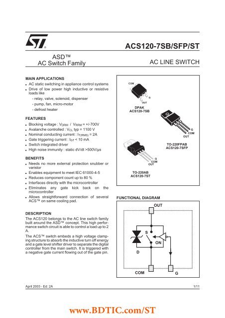
The <strong>AC</strong>S120 belongs to the <strong>AC</strong> line switch family<br />
built around the ASD concept. This high performance<br />
switch circuit is able to control a load up to 2<br />
A.<br />
The <strong>AC</strong>S switch embeds a high voltage clamping<br />
structure to absorb the inductive turn off energy<br />
and a gate level shifter driver to separate the digital<br />
controller from the main switch. It is triggered with<br />
a negative gate current flowing out of the gate pin.<br />
April 2003 - Ed: 2A<br />
<strong>AC</strong>S120-7SB/SFP/ST<br />
COM<br />
OUT<br />
G<br />
DPAK<br />
<strong>AC</strong>S120-7SB<br />
TO-220AB<br />
<strong>AC</strong>S120-7ST<br />
FUNCTIONAL DIAGRAM<br />
D<br />
S<br />
<strong>AC</strong> <strong>LINE</strong> <strong>SWITCH</strong><br />
OUT<br />
COM<br />
G<br />
www.BDTIC.com/ST<br />
OUT<br />
ON<br />
TO-220FPAB<br />
<strong>AC</strong>S120-7SFP<br />
COM G<br />
G<br />
COM<br />
OUT<br />
1/11
<strong>AC</strong>S120-7SB/SFP/ST<br />
ABSOLUTE RATINGS (limiting values)<br />
For either positive or negative polarity of pin OUT voltage in respect to pin COM voltage<br />
2/11<br />
Symbol Parameter Value Unit<br />
VDRM /VRRM Repetitive peak off-state voltage Tj = -10 °C 700 V<br />
IT(RMS) RMS on-state current full cycle sine DPAK Tc = 115 °C 2 A<br />
wave 50 to 60 Hz<br />
TO-220FPAB Tc = °C<br />
TO-220AB Tc = 115 °C<br />
ITSM Non repetitive surge peak on-state current<br />
F =50 Hz 20 A<br />
Tj initial = 25°C, full cycle sine wave<br />
F =60 Hz 11 A<br />
I 2 t Fusing capability tp = 10ms 2.2 A²s<br />
dI/dt Repetitive on-state current critical rate Tj = 125°C F = 120 Hz 50 A/μs<br />
of rise IG = 10mA (tr < 100ns)<br />
VPP Non repetitive line peak pulse voltage note 1 2 kV<br />
Tstg Storage temperature range - 40 to + 150 °C<br />
Tj Operating junction temperature range - 30 to + 125 °C<br />
Tl Maximum lead soldering temperature during 10s 260 °C<br />
Note 1: according to test described by IEC61000-4-5 standard & Figure 3.<br />
GATE CHAR<strong>AC</strong>TERISTICS (maximum values)<br />
Symbol Parameter Value Unit<br />
PG (AV) Average gate power dissipation 0.1 W<br />
IGM Peak gate current (tp = 20µs) 1 A<br />
VGM Peak positive gate voltage (in respect to pin COM) 5 V<br />
THERMAL RESISTANCES<br />
Symbol Parameter Value Unit<br />
Rth (j-a) Junction to ambient S = 0.5cm² DPAK 70 °C/W<br />
TO-220FPAB 60 °C/W<br />
TO-220AB 60 °C/W<br />
Rth (j-l) Junction to tab/lead for full cycle sine wave<br />
DPAK 2.6 °C/W<br />
conduction<br />
TO-220FPAB 3.5 °C/W<br />
TO-220AB 2.6 °C/W<br />
S = Copper surface under Tab<br />
www.BDTIC.com/ST
PARAMETER DESCRIPTION<br />
IGT<br />
VGT<br />
VGD<br />
IH<br />
IL<br />
VTM<br />
VTO<br />
Parameter Symbol Parameter description<br />
ELECTRICAL CHAR<strong>AC</strong>TERISTICS<br />
For either positive or negative polarity of pin OUT voltage in respect to pin COM voltage.<br />
<strong>AC</strong>S120-7SB/SFP/ST<br />
Symbol Test Conditions Values Unit<br />
IGT VOUT=12V (DC) RL=140Ω QII - QIII Tj=25°C MAX 10 mA<br />
VGT VOUT=12V (DC) RL=140Ω QII - QIII Tj=25°C MAX 1 V<br />
VGD VOUT=VDRM RL=3.3kΩ Tj=125°C MIN 0.15 V<br />
IH IOUT= 100mA gate open Tj=25°C MAX 45 mA<br />
IL IG= 20mA Tj=25°C MAX 65 mA<br />
VTM IOUT = 2.8A tp=380μs Tj=25°C MAX 1.3 V<br />
VTO Tj=125°C MAX 0.85 V<br />
Rd Tj=125°C MAX 200 mΩ<br />
IDRM /<br />
IRRM<br />
Triggering gate current<br />
Triggering gate voltage<br />
Non-triggering gate voltage<br />
Holding current<br />
Latching current<br />
Peak on-state voltage drop<br />
On state threshold voltage<br />
Rd On state dynamic resistance<br />
IDRM /IRRM<br />
Maximum forward or reverse leakage current<br />
dV/dt Critical rate of rise of off-state voltage<br />
(dV/dt)c Critical rate of rise of commutating off-state voltage<br />
(dI/dt)c Critical rate of decrease of commutating on-state current<br />
VCL<br />
ICL<br />
Clamping voltage<br />
Clamping current<br />
VOUT = 700V Tj=25°C MAX 2 μA<br />
Tj=125°C MAX 200<br />
dV/dt VOUT=460V gate open Tj=110°C MIN 500 V/μs<br />
(dI/dt)c (dV/dt)c = 20V/μs Tj=125°C MIN 1 A/ms<br />
VCL ICL = 1mA tp=1ms Tj=25°C TYP 1100 V<br />
www.BDTIC.com/ST<br />
3/11
<strong>AC</strong>S120-7SB/SFP/ST<br />
<strong>AC</strong> <strong>LINE</strong> <strong>SWITCH</strong> BASIC APPLICATION<br />
The <strong>AC</strong>S120 device is well adapted to Washing machine, dishwasher, tumble drier, refrigerator,<br />
air-conditioning systems, and cookware. It has been designed especially to switch on & off low power loads<br />
such as solenoid, valve, relay, dispenser, micro-motor, pump, fan and defrost heaters.<br />
Pin COM: Common drive reference to connect to the power line neutral<br />
Pin G: Switch Gate input to connect to the digital controller<br />
Pin OUT: Switch Output to connect to the load<br />
This <strong>AC</strong>S switch is triggered with a negative gate current flowing out of the gate pin G. It can be driven directly<br />
by the digital controller through a resistor as shown on the typical application diagram.<br />
Thanks to its thermal and turn off commutation performances, the <strong>AC</strong>S120 switch is able to drive with no<br />
turn off additional snubber an inductive load up to 2 A.<br />
TYPICAL APPLICATION DIAGRAM<br />
4/11<br />
L<br />
<strong>AC</strong><br />
MAINS<br />
N<br />
- Vcc<br />
D<br />
S<br />
LOAD<br />
OUT<br />
ON<br />
L<br />
R<br />
COM G<br />
HIGH INDUCTIVE <strong>SWITCH</strong>-OFF OPERATION<br />
<strong>AC</strong>S120<br />
ST72 MCU<br />
At the end of the last conduction half-cycle, the load current reaches the holding current level IH , and the<br />
<strong>AC</strong>S switch turns off. Because of the inductance L of the load, the current flows then through the avalanche<br />
diode D and decreases linearly to zero. During this time, the voltage across the switch is limited to<br />
the clamping voltage VCL.<br />
The energy stored in the inductance of the load depends on the holding current IH and the inductance (up<br />
to 10 H); it can reach about 10 mJ and is dissipated in the clamping diode section. The <strong>AC</strong>S switch sustains<br />
the turn off energy because its clamping section is designed for that purpose.<br />
www.BDTIC.com/ST<br />
M
Fig. A: Turn-off operation of the <strong>AC</strong>S120 switch<br />
with an electro-valve: waveform of the pin OUT<br />
current IOUT and voltage VOUT.<br />
IOUT<br />
<strong>AC</strong>S120-7SB/SFP/ST<br />
Fig. B: <strong>AC</strong>S120 switch static characteristic.<br />
<strong>AC</strong> <strong>LINE</strong> TRANSIENT VOLTAGE RUGGEDNESS<br />
The <strong>AC</strong>S120 switch is able to sustain safely the <strong>AC</strong> line transient voltages either by clamping the low energy<br />
spikes or by breaking over under high energy shocks, even with high turn-on current rises.<br />
The test circuit of the figure C is representative of the final <strong>AC</strong>S application and is also used to stress the<br />
<strong>AC</strong>S switch according to the IEC 61000-4-5 standard conditions. Thanks to the load, the <strong>AC</strong>S switch sustains<br />
the voltage spikes up to 2 kV above the peak line voltage. It will break over safely even on resistive<br />
load where the turn on current rise is high as shown on figure D. Such non repetitive test can be done 10<br />
times on each <strong>AC</strong> line voltage polarity.<br />
Fig. C: Overvoltage ruggedness test circuit<br />
for resistive and inductive loads according to<br />
IEC61000-4-5 standards.<br />
R = 150Ω, L = 10µH, VPP = 2kV.<br />
SURGE VOLTAGE<br />
<strong>AC</strong> <strong>LINE</strong> & GENERATOR<br />
R<br />
V<strong>AC</strong> +VPP<br />
L<br />
D<br />
S<br />
COM<br />
OUT<br />
ON<br />
<strong>AC</strong>Sxx<br />
RG = 220Ω<br />
G<br />
www.BDTIC.com/ST<br />
IH<br />
VCL<br />
VOUT<br />
Fig. D: Current and Voltage of the <strong>AC</strong>S120 during<br />
IEC61000-4-5 standard test with R, L&VPP .<br />
5/11
<strong>AC</strong>S120-7SB/SFP/ST<br />
OTHER FIGURES<br />
Maximum power dissipation vs RMS on state current.<br />
RMS on-state current vs ambient temperature, case temperature<br />
Relative variation of thermal impedance junction to ambient vs pulse duration and package<br />
Relative variation of gate trigger current vs junction temperature<br />
Relative variation of holding, latching and gate current vs junction<br />
Relative variation of dV/dt vs Tj<br />
Relative variation of (dV/dt)c vs (di/dt)c<br />
Surge peak on-state current vs number of cycles<br />
Non repetitive surge peak on-state current for a sinusoidal pulse with tp
Fig. 4: Relative variation of gate trigger current,<br />
holding current and latching versus junction<br />
temperature (typical values).<br />
4.0<br />
3.5<br />
3.0<br />
2.5<br />
2.0<br />
1.5<br />
1.0<br />
0.5<br />
0.0<br />
I GT, I H, I L[T j] / I GT, I H, I L [T j = 25°C]<br />
IGT<br />
IL & IH<br />
T (°C)<br />
j<br />
-40 -30 -20 -10 0 10 20 30 40 50 60 70 80 90 100 110 120 130<br />
Fig. 6: Relative variation of critical rate of decrease<br />
of main current versus reapplied dV/dt<br />
(typical values).<br />
5.0<br />
4.5<br />
4.0<br />
3.5<br />
3.0<br />
2.5<br />
2.0<br />
1.5<br />
1.0<br />
0.5<br />
0.0<br />
22<br />
20<br />
18<br />
16<br />
14<br />
12<br />
10<br />
8<br />
6<br />
4<br />
2<br />
0<br />
(dI/dt) c [(dV/dt) c] / Specified (dI/dt) c<br />
I TSM(A)<br />
Repetitive<br />
T =105°C<br />
ab<br />
Non repetitive<br />
T initial=25°C<br />
j<br />
(dV/dt) (V/µs)<br />
c<br />
Number of cycles<br />
VOUT=400V<br />
0 5 10 15 20 25 30 35 40 45 50<br />
Fig. 8: Surge peak on-state current versus number<br />
of cycles.<br />
t=20ms<br />
1 10 100 1000<br />
8<br />
7<br />
6<br />
5<br />
4<br />
3<br />
2<br />
1<br />
0<br />
dV/dt [T ] / dV/dt [T = 125°C]<br />
j j<br />
<strong>AC</strong>S120-7SB/SFP/ST<br />
Fig. 5: Relative variation of static dV/dt versus<br />
junction temperature.<br />
20<br />
18<br />
16<br />
14<br />
12<br />
10<br />
T (°C)<br />
j<br />
VOUT=460V<br />
25 50 75 100 125<br />
8<br />
6<br />
4<br />
2<br />
0<br />
Fig. 9: Non repetitive surge peak on-state current<br />
for a sinusoidal pulse with width tp < 10ms, and<br />
corresponding value of I²t.<br />
1000<br />
100<br />
10<br />
(dI/dt) [Tj] / (dI/dt) [T = 125°C]<br />
c c j<br />
I TSM(A),<br />
I²t (A²s)<br />
dI/dt limitation:<br />
50A/µS<br />
www.BDTIC.com/ST<br />
Fig. 7: Relative variation of critical rate of decrease<br />
of main current versus junction temperature.<br />
T (°C)<br />
j<br />
25 50 75 100 125<br />
t p(ms)<br />
T initial=25°C<br />
j<br />
1<br />
0.01 0.10 1.00 10.00<br />
ITSM<br />
I²t<br />
VOUT=400V<br />
7/11
<strong>AC</strong>S120-7SB/SFP/ST<br />
Fig. 10: On-state characteristics (maximum<br />
values).<br />
10.00<br />
1.00<br />
0.10<br />
0.01<br />
8/11<br />
I TM(A)<br />
Tj max. :<br />
V to=0.85V<br />
R d=200mΩ Tj=125°C<br />
Tj=25°C<br />
<strong>AC</strong> Switch<br />
V (V)<br />
TM<br />
0.0 0.5 1.0 1.5 2.0 2.5 3.0 3.5<br />
ORDERING INFORMATION<br />
Number of switches<br />
Fig. 11: Thermal resistance junction to ambient<br />
versus copper surface under tab (printed circuit<br />
board FR4, copper thickness: 35µm)<br />
100<br />
90<br />
80<br />
70<br />
60<br />
50<br />
40<br />
30<br />
20<br />
10<br />
0<br />
Rth (°C/W)<br />
(j-a)<br />
<strong>AC</strong>S 1 20 - 7 S X<br />
IT(RMS)<br />
20 = 2.0A<br />
VDRM<br />
7 = 700V<br />
www.BDTIC.com/ST<br />
S(cm²)<br />
DPAK<br />
0 5 10 15 20 25 30 35 40<br />
Package<br />
B = DPAK<br />
FP = TO-220FPAB<br />
T = TO-220AB<br />
Gate Sensitivity<br />
S= 10mA
P<strong>AC</strong>KAGE OUT<strong>LINE</strong> MECHANICAL DATA<br />
DPAK<br />
FOOT PRINT<br />
DPAK<br />
1.6<br />
2.3<br />
6.7<br />
2.3<br />
6.7<br />
3<br />
3<br />
1.6<br />
www.BDTIC.com/ST<br />
<strong>AC</strong>S120-7SB/SFP/ST<br />
DIMENSIONS<br />
REF. Millimeters Inches<br />
Min. Max Min. Max.<br />
A 2.20 2.40 0.086 0.094<br />
A1 0.90 1.10 0.035 0.043<br />
A2 0.03 0.23 0.001 0.009<br />
B 0.64 0.90 0.025 0.035<br />
B2 5.20 5.40 0.204 0.212<br />
C 0.45 0.60 0.017 0.023<br />
C2 0.48 0.60 0.018 0.023<br />
D 6.00 6.20 0.236 0.244<br />
E 6.40 6.60 0.251 0.259<br />
G 4.40 4.60 0.173 0.181<br />
H 9.35 10.10 0.368 0.397<br />
L2 0.80 typ. 0.031 typ.<br />
L4 0.60 1.00 0.023 0.039<br />
V2 0° 8° 0° 8°<br />
9/11
<strong>AC</strong>S120-7SB/SFP/ST<br />
P<strong>AC</strong>KAGE OUT<strong>LINE</strong> MECHANICAL DATA<br />
TO-220FPAB<br />
L3<br />
10/11<br />
L2<br />
L4<br />
G1<br />
H<br />
G<br />
F<br />
F1<br />
F2<br />
L6<br />
L5<br />
Dia<br />
D<br />
B<br />
A<br />
E<br />
L7<br />
REF.<br />
www.BDTIC.com/ST<br />
DIMENSIONS<br />
Millimeters Inches<br />
Min. Max. Min. Max.<br />
A 4.4 4.6 0.173 0.181<br />
B 2.5 2.7 0.098 0.106<br />
D 2.5 2.75 0.098 0.108<br />
E 0.45 0.70 0.018 0.027<br />
F 0.75 1 0.030 0.039<br />
F1 1.15 1.70 0.045 0.067<br />
F2 1.15 1.70 0.045 0.067<br />
G 4.95 5.20 0.195 0.205<br />
G1 2.4 2.7 0.094 0.106<br />
H 10 10.4 0.393 0.409<br />
L2 16 Typ. 0.63 Typ.<br />
L3 28.6 30.6 1.126 1.205<br />
L4 9.8 10.6 0.386 0.417<br />
L5 2.9 3.6 0.114 0.142<br />
L6 15.9 16.4 0.626 0.646<br />
L7 9.00 9.30 0.354 0.366
P<strong>AC</strong>KAGE OUT<strong>LINE</strong> MECHANICAL DATA<br />
TO-220AB<br />
L2<br />
F2<br />
F1<br />
F<br />
G1<br />
H2<br />
Dia<br />
G<br />
L5<br />
L9<br />
OTHER INFORMATION<br />
L6<br />
L4<br />
C<br />
D<br />
M<br />
A<br />
E<br />
L7<br />
<strong>AC</strong>S120-7SB/SFP/ST<br />
DIMENSIONS<br />
REF. Millimeters Inches<br />
Min. Max. Min. Max.<br />
A 4.40 4.60 0.173 0.181<br />
C 1.23 1.32 0.048 0.051<br />
D 2.40 2.72 0.094 0.107<br />
E 0.49 0.70 0.019 0.027<br />
F 0.61 0.88 0.024 0.034<br />
F1 1.14 1.70 0.044 0.066<br />
F2 1.14 1.70 0.044 0.066<br />
G 4.95 5.15 0.194 0.202<br />
G1 2.40 2.70 0.094 0.106<br />
H2 10 10.40 0.393 0.409<br />
L2 16.4 typ. 0.645 typ.<br />
L4 13 14 0.511 0.551<br />
L5 2.65 2.95 0.104 0.116<br />
L6 15.25 15.75 0.600 0.620<br />
L7 6.20 6.60 0.244 0.259<br />
L9 3.50 3.93 0.137 0.154<br />
M 2.6 typ. 0.102 typ.<br />
Diam. 3.75 3.85 0.147 0.151<br />
Ordering type Marking Package Weight Base qty Delivery mode<br />
<strong>AC</strong>S120-7SB <strong>AC</strong>S1207S DPAK 0.3 g 75 Tube<br />
<strong>AC</strong>S120-7SB-TR <strong>AC</strong>S1207S DPAK 0.3 g 2500 Tape & reel<br />
<strong>AC</strong>S120-7SFP <strong>AC</strong>S1207S TO-220FPAB 2.4 g 50 Tube<br />
<strong>AC</strong>S120-7ST <strong>AC</strong>S1207S TO-220AB 2.3 g 250 Bulk<br />
■ Epoxy meets UL94,V0<br />
Information furnished is believed to be accurate and reliable. However, STMicroelectronics assumes no responsibility for the consequences of<br />
use of such information nor for any infringement of patents or other rights of third parties which may result from its use. No license is granted by<br />
implication or otherwise under any patent or patent rights of STMicroelectronics. Specifications mentioned in this publication are subject to<br />
change without notice. This publication supersedes and replaces all information previously supplied.<br />
STMicroelectronics products are not authorized for use as critical components in life support devices or systems without express written approval<br />
of STMicroelectronics.<br />
The ST logo is a registered trademark of STMicroelectronics<br />
© 2003 STMicroelectronics - Printed in Italy - All rights reserved.<br />
STMicroelectronics GROUP OF COMPANIES<br />
Australia - Brazil - Canada - China - Finland - France - Germany<br />
Hong Kong - India - Israel - Italy - Japan - Malaysia - Malta - Morocco - Singapore<br />
Spain - Sweden - Switzerland - United Kingdom - United States.<br />
http://www.st.com<br />
www.BDTIC.com/ST<br />
11/11