PCI64 Interface v3.0.150 - Xilinx
PCI64 Interface v3.0.150 - Xilinx
PCI64 Interface v3.0.150 - Xilinx
Create successful ePaper yourself
Turn your PDF publications into a flip-book with our unique Google optimized e-Paper software.
Features<br />
• Fully PCI 3.0-compliant core, 64-bit, 66/33 MHz<br />
interface<br />
Customizable, programmable, single-chip solution<br />
Pre-defined implementation for predictable timing<br />
Incorporates <strong>Xilinx</strong> Smart-IP technology<br />
3.3V operation at 0-66 MHz<br />
5.0V operation at 0-33 MHz<br />
Fully verified design tested with <strong>Xilinx</strong> proprietary<br />
testbench and hardware<br />
Available through the <strong>Xilinx</strong> CORE Generator<br />
system v7.1i or higher<br />
CardBus compliant<br />
Supported initiator functions:<br />
- Configuration read, configuration write<br />
- Memory read, memory write, MRM, MRL<br />
- Interrupt acknowledge, special cycles<br />
- I/O read, I/O write<br />
Supported target functions:<br />
- Type 0 configuration space header<br />
- Up to three base address registers (MEM or I/O<br />
with adjustable block size from 16 bytes to 2 GB)<br />
- Medium decode speed<br />
- Parity generation, parity error detection<br />
- Configuration read, configuration write<br />
- Memory read, memory write, MRM, MRL<br />
- Interrupt acknowledge<br />
- I/O read, I/O write<br />
- Target abort, target retry, target disconnect<br />
0<br />
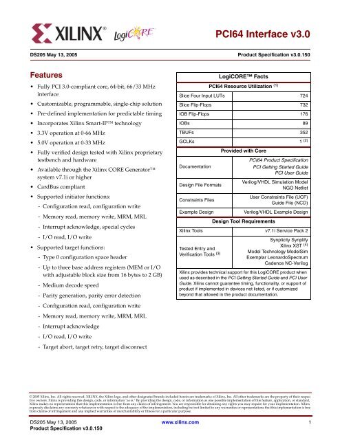
<strong>PCI64</strong> <strong>Interface</strong> v3.0<br />
DS205 May 13, 2005 0 0 Product Specification <strong>v3.0.150</strong><br />
LogiCORE Facts<br />
<strong>PCI64</strong> Resource Utilization (1)<br />
Slice Four Input LUTs 724<br />
Slice Flip-Flops 732<br />
IOB Flip-Flops 176<br />
IOBs 89<br />
TBUFs 352<br />
GCLKs 1 (2)<br />
Documentation<br />
Design File Formats<br />
Constraints Files<br />
Provided with Core<br />
<strong>PCI64</strong> Product Specification<br />
PCI Getting Started Guide<br />
PCI User Guide<br />
Verilog/VHDL Simulation Model<br />
NGO Netlist<br />
User Constraints File (UCF)<br />
Guide File (NCD)<br />
Example Design Verilog/VHDL Example Design<br />
Design Tool Requirements<br />
<strong>Xilinx</strong> Tools v7.1i Service Pack 2<br />
Tested Entry and<br />
Verification Tools (3)<br />
Synplicity Synplify<br />
<strong>Xilinx</strong> XST (4)<br />
Model Technology ModelSim<br />
Exemplar LeonardoSpectrum<br />
Cadence NC-Verilog<br />
<strong>Xilinx</strong> provides technical support for this LogiCORE product when<br />
used as described in the PCI Getting Started Guide and PCI User<br />
Guide. <strong>Xilinx</strong> cannot guarantee timing, functionality, or support of<br />
product if implemented in devices not listed, or if customized<br />
beyond that allowed in the product documentation.<br />
© 2005 <strong>Xilinx</strong>, Inc. All rights reserved. XILINX, the <strong>Xilinx</strong> logo, and other designated brands included herein are trademarks of <strong>Xilinx</strong>, Inc. All other trademarks are the property of their respective<br />
owners. <strong>Xilinx</strong> is providing this design, code, or information "as is." By providing the design, code, or information as one possible implementation of this feature, application, or standard,<br />
<strong>Xilinx</strong> makes no representation that this implementation is free from any claims of infringement. You are responsible for obtaining any rights you may require for your implementation. <strong>Xilinx</strong><br />
expressly disclaims any warranty whatsoever with respect to the adequacy of the implementation, including but not limited to any warranties or representations that this implementation is free<br />
from claims of infringement and any implied warranties of merchantability or fitness for a particular purpose.<br />
DS205 May 13, 2005 www.xilinx.com 1<br />
Product Specification <strong>v3.0.150</strong>
<strong>PCI64</strong> <strong>Interface</strong> v3.0<br />
Fact Table Notes<br />
1. Resource utilization depends on configuration of the interface and the user design. Unused resources are trimmed by the<br />
<strong>Xilinx</strong> technology mapper. The utilization figures reported in this table are representative of a maximum configuration.<br />
2. Designs running at 66 MHz in devices other than Virtex-II, Virtex-II Pro, Virtex-4, Spartan-3, and Spartan-3E require one<br />
GCLKIOB and two GCLKs. Virtex-4 implementations require additional BUFG for 200 MHz reference clock.<br />
3. See the PCI Getting Started Guide or product release notes for current supported versions.<br />
4. XST is command line option only. See the PCI Getting Started Guide for details.<br />
5. Universal card implementations require two bitstreams.<br />
6. Virtex and Spartan-II not recommended for CardBus.<br />
7. Commercial devices; 0 o C < T j < 85 o C.<br />
Table 1: Core Implementation<br />
Device Supported Power Supply<br />
<strong>PCI64</strong>/66<br />
Virtex XCV300-BG432-6C 3.3V only<br />
Virtex XCV1000-FG680-6C 3.3V only<br />
Virtex-E XCV300E-BG432-6C 3.3V only<br />
Virtex-E XCV1000E-FG680-6C 3.3V only<br />
Virtex-II 2 XCV1000-FG456-5C/I/M 3.3V only<br />
Virtex-II Pro XC2VP7-FF672-6C/I 3.3V only<br />
Virtex-II Pro XC2VP20-FF1152-6C/I 3.3V only<br />
Virtex-II Pro XC2VP30-FF1152-6C/I 3.3V only<br />
Virtex-II Pro XC2VP40-FF1152-6C/I 3.3V only<br />
Virtex-II Pro XC2VP50-FF1152-6C/I 3.3V only<br />
Virtex-4 XC4VLX25-FF668-11C/I (6,7)<br />
(regional clock based)<br />
Virtex-4 XC4VSX35-FF668-11C/I (6,7)<br />
(regional clock based)<br />
Virtex-4 XC4VFX20-FF672-11C/I (6,7)<br />
(regional clock based)<br />
3.3V only<br />
3.3V only<br />
3.3V only<br />
Spartan-II XC2S150-FG456-6C 3.3V only<br />
Spartan-II XC2S200-FG456-6C 3.3V only<br />
Spartan-IIE XC2S300E-FG456-6C 3.3V only<br />
<strong>PCI64</strong>/33<br />
Virtex XCV300-BG432-5C 3.3V, 5.0V<br />
Virtex XCV1000-FG680-5C 3.3V, 5.0V<br />
Virtex-E XCV100E-BG352-6C 3.3V only<br />
Virtex-E XCV300E-BG432-6C 3.3V only<br />
Virtex-E XCV1000E-FG680-6C 3.3V only<br />
Virtex-II 2XCV1000-FG456-4C/I/M 3.3V only<br />
Virtex-II Pro XC2VP7-FF672-5C/I 3.3V only<br />
Virtex-II Pro XC2VP20-FF1152-5C/I 3.3V only<br />
2 www.xilinx.com DS205 May 13, 2005<br />
Product Specification <strong>v3.0.150</strong>
Table 1: Core Implementation (Continued)<br />
Device Supported Power Supply<br />
Virtex-II Pro XC2VP30-FF1152-5C/I 3.3V only<br />
Virtex-II Pro XC2VP40-FF1152-5C/I 3.3V only<br />
Virtex-II Pro XC2VP50-FF1152-5C/I 3.3V only<br />
Virtex-4 XC4VLX25-FF668-10C/I (6,7)<br />
(regional clock based)<br />
Virtex-4 XC4VSX35-FF668-10C/I (6,7)<br />
(regional clock based)<br />
Virtex-4 XC4VFX20-FF672-10C/I (6,7)<br />
(regional clock based)<br />
Virtex-4 XC4VLX25-FF668-10C/I (6,7)<br />
(global clock based)<br />
Virtex-4 XC4VSX35-FF668-10C/I (6,7)<br />
(global clock based)<br />
Notes<br />
<strong>PCI64</strong> <strong>Interface</strong> v3.0<br />
1. Spartan-3 and Spartan-3E solution pending production speed files.<br />
2. For additional Part/Package combinations, see the UCF Generator in the PCI Lounge.<br />
3. XC2V1000 is supported over Military Temp. range.<br />
4. Spartan-3, Spartan-3E, and Virtex-4 devices do not contain TBUFs. The <strong>Xilinx</strong> tools automatically translate TBUFs to LUTs,<br />
and they are included in the worst case LUT count listed.<br />
5. Virtex-II Pro, Virtex-4, Spartan-3, and Spartan-3E devices are supported over commercial and industrial temperature ranges.<br />
6. Virtex-4 solution pending production speed files.<br />
7. Requires 200 MHz reference clock.<br />
Applications<br />
3.3V only<br />
3.3V only<br />
3.3V only<br />
3.3V only<br />
3.3V only<br />
Virtex-4 XC4VFX20-FF672-10C/I (6,7)<br />
(global clock based)<br />
3.3V only<br />
Spartan-II XC2S100-FG456-6C 3.3V, 5.0V<br />
Spartan-II XC2S150-FG456-6C 3.3V, 5.0V<br />
Spartan-II XC2S200-FG456-6C 3.3V, 5.0V<br />
Spartan-IIE XC2S100E-FG456-6C 3.3V only<br />
Spartan-IIE XC2S300E-FG456-6C 3.3V only<br />
Spartan-3 XC3S1000-FG456-4C/I (1) 3.3V only<br />
Spartan-3E XC3S1200E-FG400-4C/I (1) 3.3V only<br />
Embedded applications in networking, industrial, and telecommunication systems<br />
PCI add-in boards such as frame buffers, network adapters, and data acquisition boards<br />
Hot swap CompactPCI boards<br />
CardBus compliant<br />
Any application requiring a PCI interface<br />
DS205 May 13, 2005 www.xilinx.com 3<br />
Product Specification <strong>v3.0.150</strong>
<strong>PCI64</strong> <strong>Interface</strong> v3.0<br />
General Description<br />
The PCI <strong>Interface</strong> is a pre-implemented and fully tested module for <strong>Xilinx</strong> FPGAs. The pinout for each<br />
device and the relative placement of the internal logic are predefined. Critical paths are controlled by<br />
constraints and guide files to ensure predictable timing, significantly reducing the engineering time<br />
required to implement the PCI portion of your design. Resources can instead be focused on your<br />
unique user application logic in the FPGA and on the system-level design. As a result, the <strong>Xilinx</strong> PCI<br />
products minimize product development time.<br />
The core meets the setup, hold, and clock-to-timing requirements as specified in the PCI specification,<br />
and is verified through extensive simulation.<br />
Other FPGA resources that can be used in conjunction with the PCI core to enable efficient implementation<br />
of a PCI core include:<br />
Block SelectRAM memory. Blocks of on-chip ultra-fast RAM with synchronous write and<br />
dual-port RAM capabilities. Used in PCI designs to implement FIFOs.<br />
SelectRAM memory. Distributed on-chip ultra-fast RAM with synchronous write option and<br />
dual-port RAM capabilities. Used in PCI designs to implement FIFOs.<br />
Internal three-state bus capability for data multiplexing.<br />
The interface is carefully optimized for best possible performance and utilization in <strong>Xilinx</strong> FPGA<br />
devices.<br />
Smart-IP Technology<br />
Drawing on the architectural advantages of <strong>Xilinx</strong> FPGAs, <strong>Xilinx</strong> Smart-IP technology ensures the<br />
highest performance, predictability, repeatability, and flexibility in PCI designs. The Smart-IP technology<br />
is incorporated in every PCI <strong>Interface</strong>.<br />
<strong>Xilinx</strong> Smart-IP technology leverages the <strong>Xilinx</strong> architectural advantages, such as look-up tables and<br />
segmented routing, as well as floor planning information, such as logic mapping and location constraints.<br />
This technology provides the best physical layout, predictability, and performance. In addition,<br />
these features allow for significantly reduced compile times over competing architectures.<br />
To guarantee the critical setup, hold, minimum clock-to-out, and maximum clock-to-out timing, the<br />
PCI interface is delivered with Smart-IP constraint files that are unique for a device and package combination.<br />
These constraints files guide the implementation tools so that the critical paths always are<br />
within specification.<br />
<strong>Xilinx</strong> provides Smart-IP constraints files for many device and package combinations. Constraints files<br />
for unsupported device and package combinations may be generated using the web-based constraints<br />
file generator.<br />
4 www.xilinx.com DS205 May 13, 2005<br />
Product Specification <strong>v3.0.150</strong>
Functional Description<br />
<strong>PCI64</strong> <strong>Interface</strong> v3.0<br />
Figure 1 illustrates the PCI <strong>Interface</strong> partitioned into five major blocks and a user application.<br />
Figure Top x-ref 1<br />
PCI I/O INTERFACE<br />
PCI I/O <strong>Interface</strong> Block<br />
The I/O interface block handles the physical connection to the PCI bus including all signaling, input<br />
and output synchronization, output three-state controls, and all request-grant handshaking for bus<br />
mastering.<br />
User Application<br />
PAR<br />
PAR64<br />
PERR-<br />
SERR-<br />
AD[63:0]<br />
FRAME-<br />
IRDY-<br />
REQ-<br />
GNT-<br />
REQ64-<br />
ACK64-<br />
TRDY-<br />
DEVSEL-<br />
STOP-<br />
The PCI <strong>Interface</strong> provides a simple, general-purpose interface for a wide range of applications.<br />
PCI Configuration Space<br />
This block provides the first 64 bytes of Type 0, version 3.0 Configuration Space Header, as shown in<br />
Table 2, to support software-driven Plug-and-Play initialization and configuration. This includes information<br />
for Command, Status, and three Base Address Registers (BARs).<br />
The capability for extending configuration space has been built into the user application interface. This<br />
capability, including the ability to implement a capabilities pointer in configuration space, allows the<br />
user to implement functions such as power management and message signaled interrupts in the user<br />
application.<br />
Parity Generator/Checker<br />
This block generates and checks even parity across the AD bus, the CBE# lines, and the parity signals.<br />
It also reports data parity errors via PERR# and address parity errors via SERR#.<br />
Initiator State Machine<br />
Parity<br />
Generator/<br />
Checker<br />
Initiator<br />
State<br />
Machine<br />
Target<br />
State<br />
Machine<br />
Base<br />
Address<br />
Register<br />
0<br />
ADIO[63:0]<br />
Interrupt<br />
Pin and<br />
Line<br />
Register<br />
Base<br />
Address<br />
Register<br />
1<br />
PCI Configuration Space<br />
Latency<br />
Timer<br />
Register<br />
Base<br />
Address<br />
Register<br />
2<br />
Figure 1: PCI <strong>Interface</strong> Block Diagram<br />
Command/<br />
Status<br />
Register<br />
Vendor ID,<br />
Rev ID,<br />
Other User<br />
Data<br />
This block controls the PCI interface initiator functions. The states implemented are a subset of those<br />
defined in Appendix B of the PCI Local Bus Specification. The initiator control logic uses one-hot encoding<br />
for maximum performance.<br />
DS205 May 13, 2005 www.xilinx.com 5<br />
Product Specification <strong>v3.0.150</strong><br />
USER APPLICATION
<strong>PCI64</strong> <strong>Interface</strong> v3.0<br />
Target State Machine<br />
This block controls the PCI interface target functions. The states implemented are a subset of those<br />
defined in Appendix B of the PCI Local Bus Specification. The target control logic uses one-hot encoding<br />
for maximum performance.<br />
Table 2: PCI Configuration Space Header<br />
31 16 15 0<br />
Device ID Vendor ID 00h<br />
Status Command 04h<br />
BIST Header<br />
Type<br />
<strong>Interface</strong> Configuration<br />
The PCI <strong>Interface</strong> can be easily configured to fit unique system requirements using the <strong>Xilinx</strong> CORE<br />
Generator GUI or by changing the HDL configuration file. The following customization options,<br />
among many others, are supported by the interface and are described in the PCI User Guide.<br />
Device and vendor ID<br />
Base Address Registers (number, size, and type)<br />
Burst Transfer<br />
Class Code Rev ID 08h<br />
Latency<br />
Timer<br />
The PCI bus derives its performance from its ability to support burst transfers. The performance of any<br />
PCI application depends largely on the size of the burst transfer. Buffers to support PCI burst transfer<br />
can efficiently be implemented using on-chip RAM resources.<br />
Supported PCI Commands<br />
Cache Line<br />
Size<br />
Table 3 illustrates the PCI bus commands supported by the PCI <strong>Interface</strong>.<br />
6 www.xilinx.com DS205 May 13, 2005<br />
Product Specification <strong>v3.0.150</strong><br />
0Ch<br />
Base Address Register 0 (BAR0)<br />
10h<br />
Base Address Register 1 (BAR1)<br />
14h<br />
Base Address Register 2 (BAR2)<br />
18h<br />
Base Address Register 3 (BAR3)<br />
1Ch<br />
Base Address Register 4 (BAR4)<br />
20h<br />
Base Address Register 5 (BAR5)<br />
24h<br />
Cardbus CIS Pointer<br />
28h<br />
Subsystem ID Subsystem Vendor ID 2Ch<br />
Expansion ROM Base Address<br />
30h<br />
Reserved CapPtr 34h<br />
Reserved<br />
38h<br />
Max Lat Min Gnt Int Pin Int Line 3Ch<br />
Reserved<br />
Notes: Shaded areas are not implemented and return zero.<br />
40h-FFh
Bandwidth<br />
<strong>PCI64</strong> <strong>Interface</strong> v3.0<br />
The PCI <strong>Interface</strong> supports fully compliant zero wait-state burst operations for both sourcing and<br />
receiving data. This interface supports a sustained bandwidth of up to 528 MBytes/sec. The design can<br />
be configured to take advantage of the ability of the PCI <strong>Interface</strong> to do very long bursts.<br />
The flexible user application interface, combined with support for many different PCI features, gives<br />
users a solution that lends itself to use in many high-performance applications. The user is not locked<br />
into one DMA engine; hence, an optimized design that fits a specific application can be designed.<br />
Recommended Design Experience<br />
The PCI <strong>Interface</strong> is pre-implemented, allowing engineering focus on the unique user application functions<br />
of a PCI design. However, PCI is a high-performance design that is challenging to implement in<br />
any technology. For this reason, previous experience building high-performance, pipelined FPGA<br />
designs using <strong>Xilinx</strong> implementation software, constraint files, and guide files is recommended. The<br />
challenge to implement a complete PCI design including user application functions varies depending<br />
on configuration and functionality of your application. Contact your local <strong>Xilinx</strong> representative for a<br />
closer review and estimation for your specific requirements.<br />
Timing Specifications<br />
The maximum speed at which your user design is capable of running can be affected by the size and<br />
quality of the design. The following tables show the key timing parameters for the PCI <strong>Interface</strong>.<br />
Table 4 lists the Timing Parameters in the 66 MHz Implementations and Table 5 lists Timing Parameters<br />
in the 33 MHz Implementations.<br />
Table 3: PCI Bus Commands<br />
CBE [3:0] Command<br />
PCI<br />
Initiator<br />
PCI<br />
Target<br />
0000 Interrupt Acknowledge Yes Yes<br />
0001 Special Cycle Yes Ignore<br />
0010 I/O Read Yes Yes<br />
0011 I/O Write Yes Yes<br />
0100 Reserved Ignore Ignore<br />
0101 Reserved Ignore Ignore<br />
0110 Memory Read Yes Yes<br />
0111 Memory Write Yes Yes<br />
1000 Reserved Ignore Ignore<br />
1001 Reserved Ignore Ignore<br />
1010 Configuration Read Yes Yes<br />
1011 Configuration Write Yes Yes<br />
1100 Memory Read Multiple Yes Yes<br />
1101 Dual Address Cycle No Ignore<br />
1110 Memory Read Line Yes Yes<br />
1111 Memory Write Invalidate No Yes<br />
DS205 May 13, 2005 www.xilinx.com 7<br />
Product Specification <strong>v3.0.150</strong>
<strong>PCI64</strong> <strong>Interface</strong> v3.0<br />
Table 4: Timing Parameters, 66 MHz Implementation<br />
Symbol Parameter Min Max<br />
T cyc CLK Cycle Time 15 1 30<br />
T high CLK High Time 6 -<br />
T low CLK Low Time 6 -<br />
T val<br />
T val<br />
CLK to Signal Valid Delay<br />
(bussed signals)<br />
CLK to Signal Valid Delay<br />
(point to point signals)<br />
2 2 6 2<br />
2 2 6 2<br />
T on Float to Active Delay 2 2 -<br />
T off Active to Float Delay - 14 1<br />
T su<br />
T su<br />
Input Setup Time to CLK<br />
(bussed signals)<br />
Input Setup Time to CLK<br />
(point to point signals)<br />
3 2,3 -<br />
5 2,3 -<br />
T h Input Hold Time from CLK 0 2,3 -<br />
T rstoff Reset Active to Output Float - 40<br />
Notes<br />
1. Controlled by timespec constraints, included in product.<br />
2. Controlled by SelectIO configured for PCI66_3.<br />
3. Controlled by guide file, included in product.<br />
Table 5: Timing Parameters, 33 MHz Implementations<br />
Symbol Parameter Min Max<br />
T cyc CLK Cycle Time 30 1 -<br />
T high CLK High Time 11 -<br />
T low CLK Low Time 11 -<br />
T val<br />
T val<br />
CLK to Signal Valid Delay<br />
(bussed signals)<br />
CLK to Signal Valid Delay<br />
(point to point signals)<br />
2 2 11 2<br />
2 2 11 2<br />
T on Float to Active Delay 2 2 -<br />
T off Active to Float Delay - 28 1<br />
T su<br />
T su<br />
Input Setup Time to CLK<br />
(bussed signals)<br />
Input Setup Time to CLK<br />
(point to point signals)<br />
7 2 -<br />
10 2 -<br />
T h Input Hold Time from CLK 0 2 -<br />
T rstoff Reset Active to Output Float - 40<br />
Notes<br />
1. Controlled by timespec constraints, included in product.<br />
2. Controlled by SelectIO configured for PCI33_3 or PCI33_5.<br />
8 www.xilinx.com DS205 May 13, 2005<br />
Product Specification <strong>v3.0.150</strong>
Ordering Information<br />
<strong>PCI64</strong> <strong>Interface</strong> v3.0<br />
Build <strong>v3.0.150</strong> of the PCI core, with support added for Spartan-3E, is for available for download from the<br />
<strong>Xilinx</strong> IP Center, and can also be accessed through the <strong>Xilinx</strong> CORE Generator system v7.1i or higher.<br />
The <strong>Xilinx</strong> CORE Generator is bundled with the ISE Foundation v7.1i software at no additional charge.<br />
To purchase the <strong>Xilinx</strong> PCI core, please contact your local <strong>Xilinx</strong> sales representative.<br />
Part Numbers<br />
DO-DI-<strong>PCI64</strong>-IP<br />
- Access to v3.0 64-bit 66 MHz PCI Lounge IP only core support Spartan and Virtex Families<br />
Revision History<br />
The following table shows the revision history for this document.<br />
Date Version Revision<br />
08/30/02 1.2 Style update<br />
12/18/02 1.3 Updated to V3.0.103; v5.Ii, 1st feature: 32-bit was 64/32-bit<br />
3/3/03 1.4 Revised date to 3/3/03; updated to v3.0.105; v5.2i.<br />
4/14/03 1.5<br />
Updated to v3.0.106; In LogiCORE Facts table, updated <strong>PCI64</strong>/33 product listings to<br />
include Spartan-3 device support.<br />
5/8/03 1.6 Updated <strong>Xilinx</strong> tools to 5.2i SP2; added Note 10.<br />
9/17/03 1.7<br />
11/10/03 1.8<br />
Updated to v3.0.113; in LogiCORE Facts table, <strong>Xilinx</strong> Tools v6.1i SP1 was v5.2i SP2;<br />
date was May 8, 2003.<br />
Updated to v3.0.116; in Supported Products table, <strong>PCI64</strong>/66 section, Virtex-II Pro<br />
XC2VP7FF672-6C was -7C.<br />
12/17/03 1.9 Updated device support information in Facts Table (added Virtex-II Pro devices).<br />
1/7/04 1.10<br />
Updated to v3.0.117; in Supported Products table, sections <strong>PCI64</strong>/66 and <strong>PCI64</strong>/33,<br />
added Virtex-II Pro XC2VP20...through XC2VP50; updated <strong>Xilinx</strong> tools to 5.2i SP3.<br />
1/30/04 1.11 Updated to v3.0.122, updated copyright information to 2004.<br />
4/9/04 1.12<br />
4/26/04 1.13<br />
7/15/04 1.14<br />
11/11/04 1.15<br />
Updated to v3.0.126; updated <strong>Xilinx</strong> tools to 6.2i SP1; added notes 11 and 12 to<br />
Supported devices table; added suffix /I to all Virtex-II Pro devices.<br />
Updated build version to v3.0.128, updated <strong>Xilinx</strong> tools to 6.2i SP2, changed date to<br />
April 26, 2004.<br />
Updated build to v3.0.129, and added support for <strong>Xilinx</strong> tools v6.2i SP3. The data<br />
sheet is updated to the new template.<br />
Updated support for <strong>Xilinx</strong> tools v6.3i; updated PCI spec to v3.0; added Exemplar<br />
LeonardoSpectrum and Cadence NC-Verilog entry and verification tools.<br />
12/8/04 1.17 Updated to build 3.0.140 and Virtex-4 support.<br />
3/7/05 1.18 Updated to <strong>Xilinx</strong> tools 7.1i and build 3.0.145.<br />
5/13/05 2.0 Updated build to 3.0.150, added support for Spartan-3E, addition of SP2.<br />
DS205 May 13, 2005 www.xilinx.com 9<br />
Product Specification <strong>v3.0.150</strong>


