pdf 30Mb
pdf 30Mb
pdf 30Mb

Create successful ePaper yourself
Turn your PDF publications into a flip-book with our unique Google optimized e-Paper software.
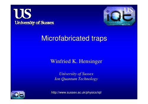
Microfabricated traps<br />
Winfried K. Hensinger<br />
University of Sussex<br />
Ion Quantum Technology<br />
http://www.sussex.ac.uk/physics/iqt/
Ion Quantum Technology at Sussex<br />
We gratefully acknowledge funding from:<br />
Sussex Ion Quantum<br />
Technology group:<br />
PI and group leader:<br />
Winfried Hensinger<br />
Grad students:<br />
Jim McLoughlin<br />
James Siverns<br />
Robin Sterling<br />
Altaf Nizamani<br />
Undergrads:<br />
Rajiv Ramasawmy<br />
Merlin Bevan-Stevenson<br />
Ben Johnson<br />
Marcus Hughes<br />
Graduated July 2007:<br />
Dan Brown, Nick Davies, Jack<br />
Friedlander, Jessica Grove-<br />
Smith, Ben Pruess, David<br />
Scrivener, Tim Short<br />
Collaborators:<br />
Jim Rabchuk, West. Illinois<br />
Keith Schwab, Cornell<br />
Chris Monroe, Maryland
Trapped Ion Quantum Computing group at the<br />
University of Michigan (now at Maryland!!)<br />
We gratefully acknowledge funding from:<br />
PI and group leader:<br />
Chris Monroe<br />
Former Postdoc, now visiting faculty:<br />
Winfried Hensinger<br />
Grad students:<br />
Jon Sterk<br />
Mark Acton<br />
Louis Deslauriers (now at Stanford)<br />
Martin Madsen (now at Wabash College)<br />
Daniel Stick (now at Sandia)<br />
Steven Olmschenk<br />
Undergrads:<br />
David Hucul (now at MIT)<br />
Jacob Burress<br />
Mark Yeo<br />
Collaborators:<br />
Jim Rabchuk, West. Illinois Univ.<br />
Keith Schwab, LPS and Cornell<br />
FOCUS
How to trap an ion<br />
Potential<br />
Position Position<br />
∇⋅ E r r<br />
=<br />
0
Charged particle trap
Trapology for beginners – an ion trap<br />
Axial confinement:<br />
Static “endcaps”<br />
Transverse confinement:<br />
Ponderomotive potential<br />
dc<br />
rf<br />
dc<br />
dc<br />
rf<br />
dc<br />
dc<br />
rf<br />
dc<br />
dc<br />
rf<br />
dc
Microfabricated traps<br />
• Electrode - ion distance<br />
- Micron dimensions<br />
• Fabrication<br />
- Photolithography<br />
- Manual assembly
Applications<br />
• Measurement based quantum computing<br />
D<br />
- high photon capture rate by getting imaging elements close to the ion<br />
coincidence<br />
photon<br />
detection<br />
D<br />
1 2<br />
|Ψ〉 = (|↓〉 1 |V〉 1 + |↑〉 1 |Η〉 1 )⊗(|↓〉 2 |V〉 2 + |↑〉 2 |Η〉 2 )<br />
upon coincidence photon detection<br />
|Ψ |Ψ〉 |Ψ ⇒ |↓〉 1 |↑〉 2 − |↑〉 2 |↓〉 2<br />
Entanglement of single-atom quantum bits at a<br />
distance, D. L. Moehring, P. Maunz, S. Olmschenk, K.<br />
C. Younge, D. N. Matsukevich, L.-M. Duan, and C.<br />
Monroe, Nature 449, 68 (2007).
Applications<br />
• Cavity quantum electrodynamics<br />
- small mode volume towards strong<br />
coupling<br />
Keller et al., Nature 431, 1075 (2004)
Applications<br />
•Ion trap transducers for quantum<br />
electromechanical oscillators<br />
Also see talk by<br />
Hartmut Haeffner<br />
W. K. Hensinger, D. Wahyu Utami, H.-S. Goan, K. Schwab, C. Monroe and G. J.<br />
Milburn, Phys. Rev. A 72, 041405(R) (2005)<br />
L. Tian, P. Rabl, R. Blatt, and P. Zoller, Phys. Rev. Lett., 92:247902 (2004)
Towards ion trap quantum<br />
computation<br />
• Deterministic 8-ion entanglement<br />
• Two-qubit Phase gate<br />
• Quantum state tomography<br />
• Quantum error correction<br />
• Ion-Photon entanglement<br />
• Teleportation<br />
• Various quantum algorithms (such as search)<br />
•<br />
•<br />
•<br />
Amazing<br />
achievements<br />
by the groups of<br />
Wineland, Blatt,<br />
Steane, Monroe<br />
and others.<br />
With help of<br />
theorists such as<br />
Chirac, Zoller,<br />
Milburn,<br />
Molmer/Sorensen<br />
and others
What’s missing?
Applications<br />
• Scaling ion trap quantum computing<br />
ENIAC<br />
(1946)
Large scale arrays<br />
Wineland et al., NIST J. Res. 103, 259 (1998)<br />
Kielpinski, Monroe and Wineland, Nature 417, 709 (2002)<br />
Steane, quant-ph/0412165
Trapology for beginners – symmetric<br />
Symmetric trap:<br />
Trap electrodes surround the ion pathway<br />
symmetrically<br />
dc<br />
rf<br />
dc<br />
dc<br />
rf<br />
dc<br />
versus asymmetric<br />
Asymmetric trap (also referred to as surface trap):<br />
Trap electrodes reside in a single plane and the ion<br />
pathway is above that plane<br />
dc rf dc dc rf dc
Fabricating ion chips<br />
Design and implementation of scalable ion trap<br />
fabrication methods is of key importance for ion trap<br />
quantum computing.<br />
Photolithography<br />
No manual assembly
gnd<br />
Two-Layer Ion Trap<br />
rf<br />
rf gnd<br />
V 0 cosWt<br />
+U<br />
0<br />
+U<br />
+U<br />
0<br />
+U
MEMS Gallium-Arsenide ion<br />
trap in a microchip<br />
60 µm<br />
D. Stick<br />
W. K. Hensinger<br />
S. Olmschenk<br />
M. Madsen<br />
K. Schwab<br />
C. Monroe
8.6 µm<br />
60 µm<br />
130 µm
Ion Trapped in a Semiconductor Chip<br />
Secular frequencies: ω/2π = 1.0 MHz, 3.3 MHz and 4.3 MHz<br />
single<br />
Cd + ion<br />
RF amplitude 8V at 15.9 MHz, Static: +1V, -0.33V<br />
Trap depth: 0.08 eV<br />
Life time: 30 min observed, 10 min typical<br />
Shuttled to adjacent electrode segment<br />
60 µm<br />
D. Stick, W. K. Hensinger, S. Olmschenk, M. J. Madsen,<br />
K. Schwab and C. Monroe, Nature Physics 2, 36 (2006)
GaAs Ion Trap Fabrication<br />
~10 mm<br />
~10 mm<br />
100 µm<br />
Si doped GaAs<br />
AlGaAs<br />
Ge:Au
GaAs Ion Trap Fabrication<br />
~10 mm<br />
~10 mm<br />
100 µm<br />
Si doped GaAs<br />
AlGaAs<br />
Ge:Au
GaAs Ion Trap Fabrication<br />
~10 mm<br />
~10 mm<br />
100 µm<br />
Si doped GaAs<br />
AlGaAs<br />
Ge:Au
MEMS Silicon ion traps<br />
53 step process!<br />
In collaboration with:<br />
Dan Stick, Jon Sterk, Martin Madsen, Winfried Hensinger, Chris Monroe, Bill<br />
Noonan, Michael Pedersen, Steve Gross, and Michael Huff
Corresponding electric circuit
53 step process!<br />
Dan Stick, Jon Sterk, Martin Madsen, Winfried Hensinger, Chris Monroe, Bill<br />
Noonan, Michael Pedersen, Steve Gross, and Michael Huff
Dan Stick, Jon Sterk, Martin Madsen, Winfried Hensinger, Chris Monroe, Bill<br />
Noonan, Michael Pedersen, Steve Gross, and Michael Huff
First chip<br />
Dan Stick, Jon Sterk, Martin Madsen, Winfried Hensinger, Chris Monroe, Bill<br />
Noonan, Michael Pedersen, Steve Gross, and Michael Huff
Ion chip efforts elsewhere<br />
(incomplete…)<br />
• NIST: Boron doped Silicon electrodes, 7070 glass insulator and anodic bonding<br />
Design and operation: D. J. Wineland, et al., in Laser Spectroscopy, Proc. XVII Int. Conf. on Laser<br />
Spectroscopy, Avemore, Scotland, pp. 393–402, J. Britton et al., arXiv:quant-ph/0605170v1 (2006)<br />
• NIST: Gold electrodes on a fused silica substrate<br />
Design and operation: S. Seidelin et al., Phys. Rev. Lett. 96, 253003 (2006)<br />
• Lucent: Silicon waver with Aluminum/Tungsten electrodes<br />
Design: J. Kim et al., Quantum Inf. Comput. 5, 515 (2005), operated at Michigan<br />
• Sandia: Gold coated tungsten electrodes on Silicon substrate<br />
Design: Proceeding of TIQC 2006, Boulder, USA, operated at Oxford, see poster Curtis et al.<br />
• MIT: Gold electrodes coated on Quartz substrate<br />
Design and operation: J. Labaziewicz et al., arXiv:quant-ph0706.3763v1 (2007)<br />
• NPL: Gold coated Silicon oxide electrodes on Silicon substrate<br />
Design: M. Brownnut et al, New Journal of Physics 8 (2006) 232, see poster Wilpers et al.
DC<br />
Contact<br />
pads<br />
NIST Planar Trap Chip<br />
Gold on fused silica<br />
low pass filters<br />
John Chiaverini, Signe Seidelin, Didi Leibfried, David Wineland (NIST)<br />
RF<br />
trapping<br />
region
Magnified trap electrodes<br />
endcap<br />
control<br />
control<br />
endcap<br />
GND<br />
NIST Planar Trap Chip<br />
RF<br />
100 µm<br />
CCD pictures of strings of Mg + ions<br />
(trapped 40 mm above surface)<br />
5 µm<br />
Seidelin et al., PRL 96, 253003 (2006).<br />
John Chiaverini, Signe Seidelin, Didi Leibfried, David Wineland
Lucent ion trap<br />
Fabricated: Dick Slusher, Lucent<br />
Operated: Dan Stick, Michigan
NPL design<br />
Monolithic microfabricated ion trap chip design for scaleable quantum processors<br />
M. Brownnutt, G. Wilpers, P. Gill, R.C. Thompson, A.G. Sinclair, New J. Phys. 8, 232(2006).
NIST racetrack trap design study<br />
2.5 mm<br />
gold on fused silica<br />
4 crosses<br />
200 Zones<br />
400 Electrodes<br />
2 separate loading zones<br />
20 zones implemented and<br />
loaded<br />
Jason Amini
Shuttling and junctions in large scale<br />
arrays – multilayer alumina traps<br />
Important for entanglement of separated ions<br />
(qubits) in the array<br />
First shuttling in two-layer geometry along a line<br />
Rowe et al., Quantum Inf. Comput. 2, 257 (2002).<br />
Barrett et al., Nature 429, 737 (2005)
A quantum algorithm…<br />
Ike Chuang, MIT
W. K. Hensinger<br />
S. Olmschenk<br />
D. Stick<br />
D. Hucul<br />
M. Yeo<br />
J. Rabchuck<br />
C. Monroe<br />
1 mm<br />
49-electrode<br />
11-zone<br />
T-junction
low<br />
400 mm
Shuttling a single atom…<br />
Laser
T-Junction ponderomotive<br />
Potential
Imaging<br />
Laser 1<br />
Making the corner<br />
500µm<br />
Imaging<br />
Laser 2<br />
W. K. Hensinger, S.<br />
Olmschenk, D. Stick, D.<br />
Hucul, M. Yeo, M. Acton, L.<br />
Deslauriers, J. Rabchuk and<br />
C. Monroe, Applied Physics<br />
Letters 88, 034101 (2006)
Voltage evolution
Simulation
Kinetic energy evolution during the turn
Separating two ions
Atomic three-point turn
The controls…
Junctions in asymmetric traps and symmetric twoand<br />
three layer traps<br />
Asymmetric<br />
(surface/planar) traps<br />
Two-layer symmetric<br />
traps<br />
Three-layer symmetric<br />
traps
NIST two layer cross trap<br />
Mg + and Be + moved through<br />
junction > 10 4 times without ion loss<br />
Characterization of heating during<br />
shuttling in progress<br />
Brad Blakestad, Didi Leibfried and<br />
David Wineland<br />
2 wafers of alumina (0.2 mm thick)<br />
gold conducting surfaces (2 µm)<br />
dc<br />
18 zones, 1 cross<br />
rf
Ulm linear multizone trap<br />
Stefan Schulz, Ulrich Poschinger, Frank Ziesel and Ferdinand Schmidt-Kaler
Scaling laws for three-layer junctions<br />
Cross-sectional view of ion trap:<br />
Aspect ratio:<br />
a/b<br />
b<br />
a<br />
D. Hucul, M. Yeo, W.K. Hensinger, J. Rabchuk, S.<br />
Olmschenk, and C. Monroe, Quantum Information<br />
and Computation 8, 0501 (2008)
Adiabatic shuttling: Which shuttling<br />
voltage time profile is the best?<br />
Average motional state n after shuttling as a function of the time to shuttle the ion T<br />
hyperbolic tan<br />
sinusoidal<br />
linear<br />
For a given shuttling time, hyperbolic tan protocol always wins<br />
D. Hucul, M. Yeo,<br />
W.K. Hensinger,<br />
J. Rabchuk, S. Olmschenk,<br />
and C. Monroe,<br />
Quantum Information and<br />
Computation 8, 0501<br />
(2008)<br />
quant-ph/0702175 (2007)
Average motional state n after shuttling as a function of the time to shuttle the ion T<br />
hyperbolic tan<br />
sinusoidal<br />
For a long enough shuttling time, sinusoidal protocol always wins
How micro can micro-traps be?<br />
What about nano-traps?
Motional heating in ion traps
Two mechanisms:<br />
Heating due to Johnson noise?<br />
S E (ω) ~ d -2<br />
Heating due to fluctuating patch potential ?<br />
S E (ω) ~ d -4<br />
Heating and spectral noise density:<br />
2<br />
2<br />
e ⎛<br />
⎞<br />
⎜<br />
z<br />
n& ω<br />
= ⎟<br />
⎜<br />
SE<br />
( ωz<br />
) + S ( Ω ± )<br />
2 E ωz<br />
4mhω<br />
⎟<br />
z ⎝ 2Ω<br />
⎠
Ion trap with adjustable electrodes<br />
23 – 250 µm<br />
Scaling and Suppression of Anomalous Quantum Decoherence in Ion Traps,<br />
L. Deslauriers, S. Olmschenk, D. Stick, W. K. Hensinger, J. Sterk, and C. Monroe,<br />
Physical Review Letters 97, 103007 (2006)
15 mm diameter needle tips
Scaling of heating with trap size:<br />
Without cooling:<br />
n& ∝<br />
Significant suppression of patch potential heating by modest cooling!<br />
zo<br />
1<br />
3<br />
. 5
MIT cryogenic surface trap<br />
Before annealing After annealing<br />
Annealing makes<br />
a big difference<br />
J. Labaziewicz, Y. Ge, P. Antohi, D. Leibrandt, K.R. Brown, and I.L. Chuang.<br />
Suppression of heating rates in cryogenic surface-electrode ion traps.<br />
Phys. Rev. Lett., 100:013001 (2008)
Field Noise [(V/m) 2 Field Noise [(V/m) /Hz] 2 /Hz]<br />
10-8 10-8 10-9 10-9 10-10 10-10 10-11 10-11 10-12 10-12 10-13 10-13 10-14 10-14 Way forward<br />
Field Noise History: 0.6 - 6.0 MHz traps<br />
SE ( ωz<br />
)<br />
Barium<br />
Mercury<br />
Ytterbium<br />
Calcium<br />
Beryllium<br />
Cadmium<br />
Cadmium (needle trap at 300K)<br />
Cadmium (needle trap at 150K)<br />
20 50 100 200 500 1000<br />
Ion-electrode spacing (µm)<br />
MIT result at<br />
4 K with<br />
electrodes<br />
annealed at<br />
760 ◦ C
Sussex Ytterbium Experiment
Versatile vacuum system for ion chip<br />
operation<br />
See poster Jim McLoughlin
Summary<br />
• Scaling ion trap quantum computing requires atomic<br />
physics – condensed matter interface.<br />
• Highly successful implementation for quantum information<br />
processing.<br />
• Microfabricated ion traps have a vast range of applications<br />
• We do have a good idea about motional heating in ion<br />
traps<br />
• Ion Quantum Technology is a vastly growing field with<br />
many opportunities
Ion Quantum Technology at Sussex<br />
We are always looking for interested students, potential<br />
postdocs, academic or commercial collaborators.<br />
Please contact us:<br />
w.k.hensinger@sussex.ac.uk<br />
More information at:<br />
http://www.sussex.ac.uk/physics/iqt/<br />
There is also a second ion trapping group at<br />
Sussex: Single-Ion-Cavity-QED group of<br />
Wolfgang Lange (see poster by Matthias<br />
Keller and Anders Mortensen).