Luís Nero Alves1,3, Rui L. Aguiar1,2, Dinis M. Santos1,2 ... - deetc
Luís Nero Alves1,3, Rui L. Aguiar1,2, Dinis M. Santos1,2 ... - deetc
Luís Nero Alves1,3, Rui L. Aguiar1,2, Dinis M. Santos1,2 ... - deetc

You also want an ePaper? Increase the reach of your titles
YUMPU automatically turns print PDFs into web optimized ePapers that Google loves.
A CMOS SIGNAL TO NOISE MEASUREMENT CIRCUIT FOR WIRELESS APPLICATIONS<br />
<strong>Luís</strong> <strong>Nero</strong> Alves 1,3 , <strong>Rui</strong> L. Aguiar 1,2 , <strong>Dinis</strong> M. Santos 1,2<br />
1 Instituto de Telecomunicações, Polo de Aveiro, Campus de Santiago, 3810 Aveiro, Portugal<br />
Tel: +351.34.377900, Fax: +351.34.377901.<br />
2 Dpt. Electrónica e Telecomunicações, Universidade de Aveiro, Campus de Santiago, 3810 Aveiro, Portugal<br />
Tel: +351.34.370200, Fax: +351.34.381128.<br />
3 Escola Superior de Tecnologia e Gestão, Instituto Politécnico de Leiria, Morro do Lena – Alto Vieiro,<br />
2400 Leiria, Portugal, Fax: +351.44.820310.<br />
Email: nero@av.it.pt, ruilaa@ua.pt, dms@ua.pt<br />
RESUMO<br />
Este artigo descreve um circuito capaz de medir a<br />
Relação Sinal Ruído em sistemas de comunicação por<br />
Infravermelhos. A relação Sinal Ruído desempenha um<br />
papel fundamental em Receptores Sectorizados por<br />
Infra-Vermelhos, pois é necessária para métodos de<br />
selecção ou combinação dos sinais vindos dos diferentes<br />
sectores ópticos. O circuito aqui descrito é capaz de<br />
estimar a razão entre a potência média do sinal adquirido<br />
pelo fotodetector e a potência de ruído presente no<br />
mesmo, apresentando uma gama dinâmica de 50dB.<br />
ABSTRACT<br />
This paper describes a circuit able to measure Signal to<br />
Noise ratios developed for Infrared (IR) applications. The<br />
Signal to Noise ratio is of major importance in<br />
IR Sectored Receivers because it provides the basis of<br />
selection or combining of signals coming from different<br />
optical sectors. This circuit estimates the ratio of the<br />
average optical signal sensed in the photo-detector and the<br />
average noise power present in the same photo-detector,<br />
with a 50dB output dynamic range<br />
I. INTRODUCTION<br />
Due to emergent wireless LAN technologies, and to the<br />
promising infrared medium, several efforts have been<br />
made in the design of optical receivers [1, 2]. The main<br />
aspect of these optical receivers is their “almost” diffuse<br />
nature of reception. However, as dominant noise sources<br />
are usually fixed (such as illumination lamps, or<br />
windows), the optical sensor is preferably composed of<br />
several photo-detectors with a small FOV, oriented in<br />
different directions. Thus most of the surrounding<br />
environment will be covered but some of the principal<br />
noise sources will still be avoided. The receiver is then<br />
responsible for processing the information from all photodetectors<br />
in order to maximize signal while minimizing<br />
noise. This is accomplished either as selecting the best<br />
optical sector (Best Sector), or by combining various<br />
optical sectors (Maximal Ratio) [3]. This<br />
selection/combination is based on the signal to noise ratio<br />
(SNR) of each optical sector [2-6]. For a Best Sector<br />
receiver, the selection is based on the best SNR presented<br />
in all the sectors. Maximal Ratio receivers produce an<br />
output proportional to the weighted sum of the signals of<br />
all the sectors, where the weights are the SNRs of each<br />
individual sector.<br />
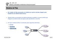
Thus a measure of the optical SNR of each sector is<br />
required in both types of sectored receivers. This SNR is<br />
proportional to the ratio of the average optical power<br />
received to the average noise power present in the photodetector,<br />
/σ. The noise power is σ 2 =2qIdcB, where q<br />
is the electron charge, Idc is the DC current component<br />
present in the PIN photo-detector due to the various<br />
natures of noise interference, and B is the system<br />
bandwidth; is proportional to the signal power.<br />
II. THE OVERALL CIRCUIT IMPLEMENTATION<br />
Current efforts in the design of IR Sectored Receivers<br />
led to the implementation of prototype versions of these<br />
systems with discrete hardware. Due to area<br />
considerations, any final version should be a low cost,<br />
low power ASIC. For cost considerations, this ASIC<br />
should be implemented with CMOS technology.<br />
Several implementation strategies were investigated on<br />
the design phase of the SNR estimator, which requires a<br />
divider. An obvious way to implement analogue division<br />
is logarithmic techniques; however, these are not easy to<br />
implement in CMOS technologies. Another possibility is<br />
the use of translinear circuits [7]. Nevertheless, translinear<br />
circuits, although simple and very accurate, do not<br />
support the desired dynamic ranges and would further<br />
exceed the power consumption budgeted. Some studies<br />
were also done around current conveyor concepts and the<br />
synthesis of mathematical functions in this domain [8, 9].<br />
This approach was abandoned due to the use of MOS<br />
transistors in the linear region and dynamic range<br />
limitations.<br />
A more classical approach uses an analogue multiplier<br />
and some non-linear feedback concepts; this proved to be<br />
suitable for our design [10]. At the heart of this circuit we<br />
have three main blocks, two multipliers and one divider.<br />
Other circuits presented in Fig.1 are responsible for signal<br />
acquisition and conditioning, polarization and voltage<br />
reference. We use differential signal paths in order to<br />
increase noise immunity and to increase the common<br />
mode rejection ratio. In this way it is possible to (although<br />
probably not desirable) to accommodate both analogue<br />
and digital processing units in the same chip. Furthermore<br />
the front-ends for which this circuit was conceived have<br />
differential topologies also [2].
The first stage, labeled N4k_cell in Fig.1 is a simple<br />
current to voltage converter, whose principal function is<br />
to measure the noise (roughly equal to DC component) in<br />
the photo-detector. This circuit has the function of lowpass<br />
filtering this noise current also (the cut-off frequency<br />
is near 2MHz). The acquired noise signal σ 2 =2qIdcB, is<br />
then fed to the divider circuit, in order to perform the 1/σ 2<br />
operation. The next step is the analogue multiplication of<br />
this pre-processed noise signal by the output signal of the<br />
front-end vs. We assume to have a linear proportionality<br />
between the current signal Is, at the photo-detector, and<br />
the vs signal (which is reasonable for most front-ends).<br />
This multiplication is done twice in order to achieve<br />
vs 2 /σ 2 , the square of the Signal to Noise Ratio.<br />
There are several reasons to measure the squared SNR<br />
and not the SNR itself. First, it is not easy to implement<br />
square root extraction circuits for the whole dynamic<br />
range we have in infrared applications. Second, if this<br />
circuit is to be used in a Best Sector receiver, it is<br />
desirable to have unipolar quantities to simplify the<br />
discrimination step. If the target is a Maximal Ratio<br />
receiver, this same signal can be applied to an AGC<br />
(automatic gain controlled amplifier).<br />
The blocks labeled Average_cell are responsible for the<br />
polarization of the multiplier cells. This polarization<br />
scheme is based on actual incoming signals, and makes<br />
the circuit more robust and less dependent on signal<br />
levels. Finally the block labeled Reg_ref_cell is<br />
responsible for all the necessary voltage references in the<br />
circuit. We choose to have these references produced<br />
inside the chip so they could be more accurate. The<br />
reference circuit is a simple series regulator, capable of a<br />
22% regulation factor.<br />
Fig. 1 Overall Circuit<br />
Finally a circuit for low-pass filtering of the final SNR<br />
squared result (filter_cell) is present in Fig.1. This<br />
filtering is needed to have an average expectation of the<br />
optical SNR. Furthermore, the cutoff frequency of this<br />
first order low pass filter can be adjusted externally<br />
according signals to process.<br />
III. THE DIFFERENTIAL MULTIPLIER<br />
The multiplier cell is basically a folded Gilbert<br />
multiplier as can be seen on Fig.2. The folded<br />
configuration was preferred to the usual form due to its<br />
larger dynamic ranges (both at the input and output). The<br />
core of the multiplier is composed of transistors NMOS<br />
M1 to M4, and PMOS M5 and M6. Transistors NMOS<br />
M7 to M10 are used with two purposes: establishing the<br />
circuit dynamic polarization and correcting the quadratic<br />
non-linearity exhibited in the fundamental Gilbert cell<br />
[11-13]. This way we could achieve a multiplier circuit<br />
with high degree of linearity inside the proposed input<br />
voltage range (1.5V to 3.5V).<br />
The differential output current is achieved through a<br />
cross-connected current mirror. Finally, a resistor and a<br />
fixed voltage reference do the current to voltage<br />
conversion.<br />
IV. THE DIVIDER CIRCUIT<br />
The divider circuit is a classical example of non-linear<br />
feedback theory. Analogue division can be achieved<br />
through the use of a multiplier placed in the feedback loop<br />
of an operational amplifier, as showed on Fig.3. The<br />
design of this circuit was a major problem due to its<br />
natural tendency to exhibit oscillations. This was<br />
corrected through the reduction of the bandwidth and gain
Fig. 3 Divider circuit<br />
of the operational amplifier to values of 40 dB and<br />
700KHz.<br />
V. The Low Pass Filter<br />
The low pass filter is needed to smooth the output signal.<br />
The input signals may exhibit several duty cycle<br />
specifications, according to the type of code used (e.g.<br />
25% for 4-PPM signals), so this filter should permit a<br />
cutoff adjustment. This feature is accomplished trough the<br />
variable feedback configuration represented in Fig. 4 [14].<br />
The cutoff adjustment is controlled solely by one external<br />
voltage (vc), and permits an almost one decade span, from<br />
near 100KHz to 1MHz.<br />
VI. SIMULATION RESULTS<br />
This circuit was implemented in AMS 0.8μm CMOS<br />
double poly, double metal technology, using the Cadence<br />
DFII environment and the SpectreS simulator, and is<br />
currently in fabrication. The following sections show the<br />
simulation results achieved.<br />
Fig. 2 Differential multiplier based on the Gilbert Multiplier cell<br />
A. The Multiplier<br />
Fig. 4 Low pass Filter<br />
Fig. 5 shows the good linearity of the multiplier<br />
transient response. This figure represents the AM product<br />
of two waves: a square wave (the carrier) at 1MHz, with<br />
amplitude of 1V and offset of 2.5V, and a sine wave (the<br />
modulating signal) at 100kHz with amplitude of 500mV<br />
and offset of 2.5V. The product of these two waves is an<br />
AM signal with almost 1V of amplitude and offset near<br />
2.5V. We should point out that in our target application<br />
(keeping this AM analogy) the carrier is the PPM signal at<br />
the output of the optical front end, and the modulating<br />
signal is the measured average noise present at the<br />
systems input.<br />
In Fig. 6 we show both signal excursions, at the input<br />
1.5V to 3.5V and at the output 1.5V to 3.5V. The<br />
expected input dynamic range is about 20dB (the output<br />
signal from the front end lies in the range of 80mV to 1V<br />
with 2.5V of offset). The output dynamic range can span<br />
more than 50dB (from 3mV to 1V). Outside the referred<br />
output range the values will not be of interest to IR
applications: these would signify either extremely good or<br />
extremely poor SNR, and thus further signal processing in<br />
such sectors is immediate.<br />
We also measured the rise time exhibited by this<br />
multiplier. Both rise and fall times fall in the range of 7ns<br />
to 10ns. The circuit bandwidth is always superior to<br />
20MHz, and shows the expected small variations with the<br />
input signal amplitude. These values exceed the<br />
maximum requirements presented in the wireless LAN<br />
applications we targeted.<br />
B. The Divider<br />
The divider DC response is depicted in Fig. 7 where we<br />
can see the approximated 1/x function. The input and<br />
output excursions are respectively 1μA to 300μA (50dB)<br />
and 2.5V to 4V (50dB). The divider’s bandwidth is<br />
limited to 2MHz. This limit is imposed by two factors: i)<br />
it is desirable to have a filtering effect over the measured<br />
input noise, and ii) the system may become unstable with<br />
larger bandwidths.<br />
C. The Low Pass Filter<br />
Fig. 5 Multiplier Transient Response<br />
Fig. 6 Multiplier DC Response<br />
Fig. 8 shows the AC response of the low pass filter.<br />
There can be seen several cutoff frequencies depending<br />
on the output control voltage Vlpf. For values of Vlpf in<br />
the range of 4V to 5V, the corresponding cutoff frequency<br />
varies from 100KHz to 1.14MHz, slightly more than one<br />
decade of adjustment.<br />
D. The SNR Measurement Circuit<br />
Fig. 9 (in the following page) shows the overall system<br />
performance, when the input signal has constant<br />
Fig. 7 Divider DC Response<br />
Fig. 8 Low Pass Filter AC Response<br />
amplitude (/net9), and noise has a trapezoidal periodic<br />
pattern (/I4/In). The desired squared SNR is represented<br />
in signals /net25 and /net27, as a differential signal. The<br />
signal /net6 represents the filtered output, with a cutoff<br />
frequency off 800KHz.<br />
The circuit was simulated with different models (worst<br />
speed, worst power) and proved to be robust to process<br />
changes. Some simulations were made adding noise to the<br />
power lines and with extreme input signals; in these<br />
extreme situations the circuit still produced useful<br />
outputs.<br />
The power consumption is expected to be in the range<br />
of 36mW and the layout area of 1000μm×500μm (see<br />
Fig. 10). For an eight-sector IR receiver, total power<br />
would be in the 270mW range.<br />
VII. CONCLUSIONS<br />
This paper describes a SNR measurement system for<br />
optical sectored receivers, with a 50dB output dynamic<br />
range. We discussed the basic blocks of the system and<br />
several design constraints. The final result is a circuit<br />
implemented with a divider in the feedback loop, with a<br />
fairly good linear response. The desired SNR evaluation<br />
is achieved even in the extreme cases found in IR<br />
networks.<br />
VIII. ACKNOWLEDGEMENTS<br />
The authors thank António M. R. Tavares for his<br />
constructive comments to the first part of this article.
Fig. 9 Overall Circuit Transient Response<br />
REFERENCES<br />
[1] Joseph M. Khan, John R. Barry, “Wireless Infrared<br />
Communications”, Proceedings of the IEEE, Vol. 85, Nº2,<br />
February 97.<br />
[2] <strong>Rui</strong> L. Aguiar, António Tavares, José L. Cura, Eduardo de<br />
Vasconcelos, Luis <strong>Nero</strong> Alves, <strong>Rui</strong> Valadas, <strong>Dinis</strong> M.<br />
Santos, “Considerations on the design of transceivers for<br />
wireless optical LANs”, IEE Colloquium on Optical<br />
Wireless Communications, London, England, Jun 99.<br />
[3] <strong>Rui</strong> J. M. T. Valadas, A. M. de Oliveira Duarte, “Sectored<br />
receivers for indoor wireless optical communication<br />
systems”, Proceedings of the Fifth IEEE International<br />
Symposium on Personal, Indoor and Mobile Radio<br />
Communications (PIMRC’94), The Hague, Netherlands,<br />
94.<br />
[4] <strong>Rui</strong> J. M. T. Valadas, “Redes de Comunicações de Área<br />
Local não- cabladas por raios Infravermelhos”, Phd Thesis,<br />
Universidade de Aveiro, November 95.<br />
Fig. 10 Circuit Layout<br />
[5] António M. R. Tavares, <strong>Rui</strong> J. M. T. Valadas, A. M. de<br />
Oliveira Duarte, “Design and Implementation of a Maximal<br />
ratio angle-diversity Receiver for Optical Wireless<br />
Communication Systems.”, Wireless Technologies and<br />
Systems: Millimeter-wave and Optical, Proceedings of<br />
SPIE, vol..3232, Dallas, Texas,Nov. 5, 97.<br />
[6] <strong>Rui</strong> J. M. T. Valadas, António M. R. Tavares, A. M. de<br />
Oliveira Duarte, “Angle Diversity to Combat Ambient<br />
Noise in Indoor Optical Wireless Communication<br />
Systems”, International Journal of Wireless Information<br />
Networks, Vol. 4, Nº 4, 1997.<br />
[7] R.J.Wiegerink, E. Seevinck, “Analysis and Synthesis of<br />
MOS Translinear Circuits”, Kluwer Academic Publishers,<br />
1993.<br />
[8] S.-L. Liu, J.-J. Chen, “Realisation of a Analogue Divider<br />
using Current Feedback Amplifiers”, IEEE Proceedings on<br />
Circuits Devices and Systems, Vol. 142, Nº1, February 95.<br />
[9] W. Chiu, S.-L. Liu, H.-W. Tsao, J.-J. Chen, “CMOS<br />
Differential Difference Current Conveyors and their<br />
Applications”, IEEE Proceedings on Circuits Devices and<br />
Systems, Vol. 143, Nº2, April 96.<br />
[10] <strong>Luís</strong> <strong>Nero</strong> Alves, “Implementação de um Circuito para<br />
Medição de Relação Sinal Ruído em Receptores Ópticos”,<br />
Internal Report, Instituto de Telecomunicações, Aveiro,<br />
December 98.<br />
[11] Carver Mead, “Analog VLSI and Neural Systems”,<br />
Addison-Wesley, 1989.<br />
[12] R. Gregorian, G. C. Temes, “Analog Mos Integrated<br />
Circuits for Signal Processing”, John Wiley & Sons 86.<br />
[13] W. Sansen, J. H. Huijsing, R. J. van der Plassche, “ Analog<br />
Circuit Design, MOST RF circuits, Sigma-Delta<br />
converters, and Translinear circuits”, Kluwer Academic<br />
Press, 1996.<br />
[14] José E. Franca, Yannis Tsividis, “ Design of Analog-<br />
Digital VLSI Circuits for Telecommunications and Signal<br />
Processing”, 2ed, Prentice Hall, 1994