

Enhanced Polymer Passivation Layer for Wafer Level Chip Scale ...
Enhanced Polymer Passivation Layer for Wafer Level Chip Scale ...
Enhanced Polymer Passivation Layer for Wafer Level Chip Scale ...

Create successful ePaper yourself
Turn your PDF publications into a flip-book with our unique Google optimized e-Paper software.
8. Pattern characterization: The substrate was inspected using a microscope to determine<br />
the quality of the developed features. A stylus-type profilometer was used to measure the<br />
height of the features.<br />
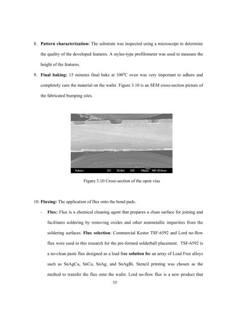
9. Final baking: 15 minutes final bake at 100 o C oven was very important to adhere and<br />
completely cure the material on the wafer. Figure 3.10 is an SEM cross-section picture of<br />
the fabricated bumping sites.<br />
Figure 3.10 Cross-section of the open vias<br />
10. Fluxing: The application of flux onto the bond pads.<br />
- Flux: Flux is a chemical cleaning agent that prepares a clean surface <strong>for</strong> joining and<br />
facilitates soldering by removing oxides and other nonmetallic impurities from the<br />
soldering surfaces. Flux selection: Commercial Kester TSF-6592 and Lord no-flow<br />
flux were used in this research <strong>for</strong> the pre-<strong>for</strong>med solderball placement. TSF-6592 is<br />
a no-clean paste flux designed as a lead free solution <strong>for</strong> an array of Lead Free alloys<br />
such as SnAgCu, SnCu, SnAg, and SnAgBi. Stencil printing was chosen as the<br />
method to transfer the flux onto the wafer. Lord no-flow flux is a new product that<br />
55


