

Enhanced Polymer Passivation Layer for Wafer Level Chip Scale ...
Enhanced Polymer Passivation Layer for Wafer Level Chip Scale ...
Enhanced Polymer Passivation Layer for Wafer Level Chip Scale ...

You also want an ePaper? Increase the reach of your titles
YUMPU automatically turns print PDFs into web optimized ePapers that Google loves.
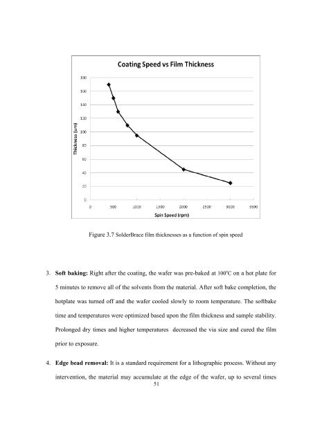
Figure 3.7 SolderBrace film thicknesses as a function of spin speed<br />
3. Soft baking: Right after the coating, the wafer was pre-baked at 100 o C on a hot plate <strong>for</strong><br />
5 minutes to remove all of the solvents from the material. After soft bake completion, the<br />
hotplate was turned off and the wafer cooled slowly to room temperature. The softbake<br />
time and temperatures were optimized based upon the film thickness and sample stability.<br />
Prolonged dry times and higher temperatures decreased the via size and cured the film<br />
prior to exposure.<br />
4. Edge bead removal: It is a standard requirement <strong>for</strong> a lithographic process. Without any<br />
intervention, the material may accumulate at the edge of the wafer, up to several times<br />
51


