

Enhanced Polymer Passivation Layer for Wafer Level Chip Scale ...
Enhanced Polymer Passivation Layer for Wafer Level Chip Scale ...
Enhanced Polymer Passivation Layer for Wafer Level Chip Scale ...
SHOW LESS

You also want an ePaper? Increase the reach of your titles
YUMPU automatically turns print PDFs into web optimized ePapers that Google loves.
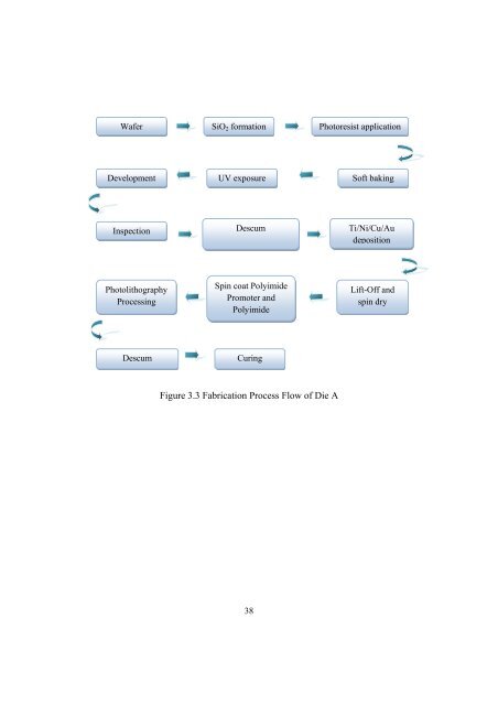
<strong>Wafer</strong> SiO2 <strong>for</strong>mation Photoresist application<br />
Development<br />
Photolithography<br />
Processing<br />
UV exposure<br />
Inspection Descum Ti/Ni/Cu/Au<br />
deposition<br />
Spin coat Polyimide<br />
Promoter and<br />
Polyimide<br />
Descum Curing<br />
Figure 3.3 Fabrication Process Flow of Die A<br />
38<br />
Soft baking<br />
Lift-Off and<br />
spin dry


