

Enhanced Polymer Passivation Layer for Wafer Level Chip Scale ...
Enhanced Polymer Passivation Layer for Wafer Level Chip Scale ...
Enhanced Polymer Passivation Layer for Wafer Level Chip Scale ...

Create successful ePaper yourself
Turn your PDF publications into a flip-book with our unique Google optimized e-Paper software.
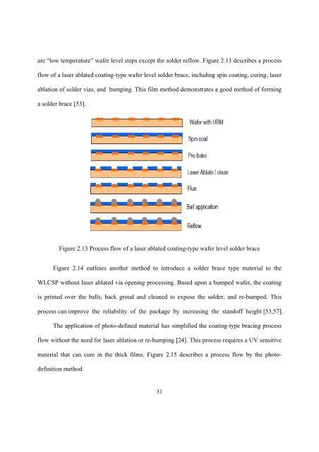
are “low temperature” wafer level steps except the solder reflow. Figure 2.13 describes a process<br />
flow of a laser ablated coating-type wafer level solder brace, including spin coating, curing, laser<br />
ablation of solder vias, and bumping. This film method demonstrates a good method of <strong>for</strong>ming<br />
a solder brace [53].<br />
Figure 2.13 Process flow of a laser ablated coating-type wafer level solder brace<br />
Figure 2.14 outlines another method to introduce a solder brace type material to the<br />
WLCSP without laser ablated via opening processing. Based upon a bumped wafer, the coating<br />
is printed over the balls, back groud and cleaned to expose the solder, and re-bumped. This<br />
process can improve the reliability of the package by increasing the standoff height [53,57].<br />
The application of photo-defined material has simplified the coating-type bracing process<br />
flow without the need <strong>for</strong> laser ablation or re-bumping [24]. This process requires a UV sensitive<br />
material that can cure in the thick films. Figure 2.15 describes a process flow by the photo-<br />
definition method.<br />
31


