Enhanced Polymer Passivation Layer for Wafer Level Chip Scale ...
Enhanced Polymer Passivation Layer for Wafer Level Chip Scale ... Enhanced Polymer Passivation Layer for Wafer Level Chip Scale ...
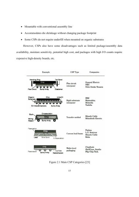
these categorized packages as well as their manufactures are given in Figure 2.1. Lead frame, flex and rigid substrate CSPs occupy the bulk of the current CSP market due to their better fit into the current packaging infrastructure. These CSP packages are processed as conventional packages. However, the most intriguing CSPs are the wafer level assembly type in which the area array “package“ is manufactured and usually tested on the wafer before dicing [6]. The CSP (shown in Figure 2.2 as a flex interposer type) is a cost effective first level package. It is often used for single or dynamic random access memories, lower I/O count microprocessors, and flash memories. Typical packages are those with a pin count in the range of 4 to 256 with sizes between 2 and 21 mm per side [23]. 2.1.2 Advantages and Disadvantages Chip Scale Packages combine the best of flip chip assembly and surface mount technology. In comparison to the standard surface mount technology, CSPs have the following advantages [26]: Reduced footprint and thickness Reduced weight Relatively easier assembly process lower over-all production costs Better electrical performance Area array distribution of connections (for most CSPs) In comparison to the bare die assembly, CSPs have the advantages such as [27]: Reworkability Encapsulated package Testability 14
Mountable with conventional assembly line Accommodates die shrinkage without changing package footprint Some CSPs do not require underfill when mounted on organic substrates However, CSPs also have some disadvantages such as limited package/assembly data availability, moisture sensitivity, potential high cost, and packages with high I/O counts require expensive high-density boards, etc. Figure 2.1 Main CSP Categories [23] 15
- Page 1 and 2: Enhanced Polymer Passivation Layer
- Page 3 and 4: SolderBrace coatings were low tempe
- Page 5 and 6: Table of Contents Abstract ........
- Page 7 and 8: 4.4 Failure Analysis ..............
- Page 9 and 10: List of Figures Figure 1.1 Trends i
- Page 11 and 12: Figure 3.17 SAC305 Reflow profile .
- Page 13 and 14: CHAPTER 1 INTRODUCTION In the era o
- Page 15 and 16: This effect changes the package to
- Page 17 and 18: 1.4 Solder Joint Fatigue Figure 1.2
- Page 19 and 20: leading to the solder joint failure
- Page 21 and 22: umped wafers. The coating is stenci
- Page 23 and 24: 11 Bumped Wafer Print over ball Pre
- Page 25: 2.1 Chip Scale Package Technology C
- Page 29 and 30: Figure 2.3 Cross section of a typic
- Page 31 and 32: Table 2.1 Comparison between tradit
- Page 33 and 34: In-Situ Bumped Wafers Placed Prefor
- Page 35 and 36: of solder joint failure, and they o
- Page 37 and 38: (a) (b) Figure 2.8(a). Metalized ph
- Page 39 and 40: "underfilled" structure distributes
- Page 41 and 42: have generally been the modificatio
- Page 43 and 44: are “low temperature” wafer lev
- Page 45 and 46: 2.3.4 Optimized SolderBrace Materia
- Page 47 and 48: CHAPTER 3 WLCSP DIE FABRCIATION In
- Page 49 and 50: Table 3.1 Test Die used for Reliabi
- Page 51 and 52: Figure 3.4 Fabrication Process Flow
- Page 53 and 54: spin coating. A layer of light sens
- Page 55 and 56: layer, is investigated as a potenti
- Page 57 and 58: 10. Final cleaning: After the passi
- Page 59 and 60: Cyclopentanone, a colorless liquid
- Page 61 and 62: used to check the basic spin and ph
- Page 63 and 64: Figure 3.7 SolderBrace film thickne
- Page 65 and 66: 6. Post-UV exposure bake: This step
- Page 67 and 68: 8. Pattern characterization: The su
- Page 69 and 70: offers the optimum flux release cha
- Page 71 and 72: fatigue resistance, lower cost SAC
- Page 73 and 74: Figure 3.12 Solder Ball Placement M
- Page 75 and 76: of solder balls to the holes on the
Mountable with conventional assembly line<br />
Accommodates die shrinkage without changing package footprint<br />
Some CSPs do not require underfill when mounted on organic substrates<br />
However, CSPs also have some disadvantages such as limited package/assembly data<br />
availability, moisture sensitivity, potential high cost, and packages with high I/O counts require<br />
expensive high-density boards, etc.<br />
Figure 2.1 Main CSP Categories [23]<br />
15


