- Page 1 and 2: Enhanced Polymer Passivation Layer
- Page 3 and 4: SolderBrace coatings were low tempe
- Page 5 and 6: Table of Contents Abstract ........
- Page 7 and 8: 4.4 Failure Analysis ..............
- Page 9 and 10: List of Figures Figure 1.1 Trends i
- Page 11 and 12: Figure 3.17 SAC305 Reflow profile .
- Page 13 and 14: CHAPTER 1 INTRODUCTION In the era o
- Page 15 and 16: This effect changes the package to
- Page 17 and 18: 1.4 Solder Joint Fatigue Figure 1.2
- Page 19 and 20: leading to the solder joint failure
- Page 21: umped wafers. The coating is stenci
- Page 25 and 26: 2.1 Chip Scale Package Technology C
- Page 27 and 28: Mountable with conventional assembl
- Page 29 and 30: Figure 2.3 Cross section of a typic
- Page 31 and 32: Table 2.1 Comparison between tradit
- Page 33 and 34: In-Situ Bumped Wafers Placed Prefor
- Page 35 and 36: of solder joint failure, and they o
- Page 37 and 38: (a) (b) Figure 2.8(a). Metalized ph
- Page 39 and 40: "underfilled" structure distributes
- Page 41 and 42: have generally been the modificatio
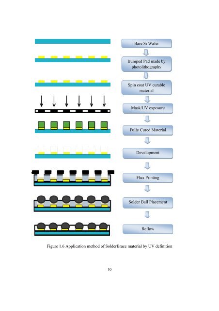
- Page 43 and 44: are “low temperature” wafer lev
- Page 45 and 46: 2.3.4 Optimized SolderBrace Materia
- Page 47 and 48: CHAPTER 3 WLCSP DIE FABRCIATION In
- Page 49 and 50: Table 3.1 Test Die used for Reliabi
- Page 51 and 52: Figure 3.4 Fabrication Process Flow
- Page 53 and 54: spin coating. A layer of light sens
- Page 55 and 56: layer, is investigated as a potenti
- Page 57 and 58: 10. Final cleaning: After the passi
- Page 59 and 60: Cyclopentanone, a colorless liquid
- Page 61 and 62: used to check the basic spin and ph
- Page 63 and 64: Figure 3.7 SolderBrace film thickne
- Page 65 and 66: 6. Post-UV exposure bake: This step
- Page 67 and 68: 8. Pattern characterization: The su
- Page 69 and 70: offers the optimum flux release cha
- Page 71 and 72: fatigue resistance, lower cost SAC
- Page 73 and 74:
Figure 3.12 Solder Ball Placement M
- Page 75 and 76:
of solder balls to the holes on the
- Page 77 and 78:
of thermal shock. If the temperatur
- Page 79 and 80:
Figure 3.17 SAC305 Reflow profile -
- Page 81 and 82:
foaming and high performance cleane
- Page 83 and 84:
- Polish clean: used the optimized
- Page 85 and 86:
Figure 3.22 SolderBrace printed waf
- Page 87 and 88:
Voids Figure 3.25 SolderBrace Mater
- Page 89 and 90:
cutting speed was set at a low valu
- Page 91 and 92:
Figure 4.2 Process Flow of Board As
- Page 93 and 94:
pitch, and bump diameter), and subs
- Page 95 and 96:
4.2.4 X-Ray Inspection Figure 4.5 R
- Page 97 and 98:
Figure 4.6 Air to air thermal cycli
- Page 99 and 100:
Figure 4.7 Thermal Cycling Setup 87
- Page 101 and 102:
4.4 Failure Analysis The main purpo
- Page 103 and 104:
Figure 4.10 Pad cratering failure o
- Page 105 and 106:
CHAPTER 5 FINITE ELEMENT ANALYSIS I
- Page 107 and 108:
5.1.1 Modeling Approaches Due to th
- Page 109 and 110:
are shown in Figure 5.2. However, t
- Page 111 and 112:
5.1.2 Material Properties Many pack
- Page 113 and 114:
strain rate sensitivity. The evolut
- Page 115 and 116:
Morris et a1 [96] used a double pow
- Page 117 and 118:
focus on the time-dependent effects
- Page 119 and 120:
5.2 Modeling Procedure In this proj
- Page 121 and 122:
Figure 5.6 The diagonal symmetry mo
- Page 123 and 124:
5.2.3 Meshing Table 5.2 Anand const
- Page 125 and 126:
direction, but that the surface is
- Page 127 and 128:
PREP7 tref,398 ! set zero strain te
- Page 129 and 130:
5.2.7 Thermal Fatigue Life Predicti
- Page 131 and 132:
CHAPTER 6 CONCLUSIONS Wafer level c
- Page 133 and 134:
References 1. Future Trends in Elec
- Page 135 and 136:
23. Electronic Packaging and Interc
- Page 137 and 138:
48. Ultra Low Stress and Low Temper
- Page 139 and 140:
70. Factors for Successful Wafer-Le
- Page 141 and 142:
92. Microstructural Dependendence o
- Page 143:
111. Nonlinear Analysis of Full Mat