Enhanced Polymer Passivation Layer for Wafer Level Chip Scale ...
Enhanced Polymer Passivation Layer for Wafer Level Chip Scale ... Enhanced Polymer Passivation Layer for Wafer Level Chip Scale ...
Figure 4.8 Weibull plot of SolderBrace coated WLCSP vs. standard WLCSP at Thermal Cycling Test Table 4.3 Summary of Thermal Cycling Test Results Die Last Failure Characteristic Life Shape parameter Non-Coated 328 cycles 13 1.4 Coated 681 cycles 510 4.7 88
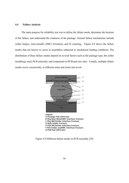
4.4 Failure Analysis The main purpose for reliability test was to define the failure mode, determine the location of the failure, and understand the weakness of the package. General failure mechanisms include solder fatigue, inter-metallic (IMC) formation, and Si cratering,. Figure 4.9 shows the failure modes that are known to occur in assemblies subjected to mechanical loading conditions. The distribution of these failure modes depend on several factors such as the package type, the solder metallurgy used, PCB materials, and component-to-PCB-pad size ratio. Usually, multiple failure modes occur concurrently, at different strain and strain rate levels. Figure 4.9 Different failure modes in PCB assembly [78] 89
- Page 49 and 50: Table 3.1 Test Die used for Reliabi
- Page 51 and 52: Figure 3.4 Fabrication Process Flow
- Page 53 and 54: spin coating. A layer of light sens
- Page 55 and 56: layer, is investigated as a potenti
- Page 57 and 58: 10. Final cleaning: After the passi
- Page 59 and 60: Cyclopentanone, a colorless liquid
- Page 61 and 62: used to check the basic spin and ph
- Page 63 and 64: Figure 3.7 SolderBrace film thickne
- Page 65 and 66: 6. Post-UV exposure bake: This step
- Page 67 and 68: 8. Pattern characterization: The su
- Page 69 and 70: offers the optimum flux release cha
- Page 71 and 72: fatigue resistance, lower cost SAC
- Page 73 and 74: Figure 3.12 Solder Ball Placement M
- Page 75 and 76: of solder balls to the holes on the
- Page 77 and 78: of thermal shock. If the temperatur
- Page 79 and 80: Figure 3.17 SAC305 Reflow profile -
- Page 81 and 82: foaming and high performance cleane
- Page 83 and 84: - Polish clean: used the optimized
- Page 85 and 86: Figure 3.22 SolderBrace printed waf
- Page 87 and 88: Voids Figure 3.25 SolderBrace Mater
- Page 89 and 90: cutting speed was set at a low valu
- Page 91 and 92: Figure 4.2 Process Flow of Board As
- Page 93 and 94: pitch, and bump diameter), and subs
- Page 95 and 96: 4.2.4 X-Ray Inspection Figure 4.5 R
- Page 97 and 98: Figure 4.6 Air to air thermal cycli
- Page 99: Figure 4.7 Thermal Cycling Setup 87
- Page 103 and 104: Figure 4.10 Pad cratering failure o
- Page 105 and 106: CHAPTER 5 FINITE ELEMENT ANALYSIS I
- Page 107 and 108: 5.1.1 Modeling Approaches Due to th
- Page 109 and 110: are shown in Figure 5.2. However, t
- Page 111 and 112: 5.1.2 Material Properties Many pack
- Page 113 and 114: strain rate sensitivity. The evolut
- Page 115 and 116: Morris et a1 [96] used a double pow
- Page 117 and 118: focus on the time-dependent effects
- Page 119 and 120: 5.2 Modeling Procedure In this proj
- Page 121 and 122: Figure 5.6 The diagonal symmetry mo
- Page 123 and 124: 5.2.3 Meshing Table 5.2 Anand const
- Page 125 and 126: direction, but that the surface is
- Page 127 and 128: PREP7 tref,398 ! set zero strain te
- Page 129 and 130: 5.2.7 Thermal Fatigue Life Predicti
- Page 131 and 132: CHAPTER 6 CONCLUSIONS Wafer level c
- Page 133 and 134: References 1. Future Trends in Elec
- Page 135 and 136: 23. Electronic Packaging and Interc
- Page 137 and 138: 48. Ultra Low Stress and Low Temper
- Page 139 and 140: 70. Factors for Successful Wafer-Le
- Page 141 and 142: 92. Microstructural Dependendence o
- Page 143: 111. Nonlinear Analysis of Full Mat
4.4 Failure Analysis<br />
The main purpose <strong>for</strong> reliability test was to define the failure mode, determine the location<br />
of the failure, and understand the weakness of the package. General failure mechanisms include<br />
solder fatigue, inter-metallic (IMC) <strong>for</strong>mation, and Si cratering,. Figure 4.9 shows the failure<br />
modes that are known to occur in assemblies subjected to mechanical loading conditions. The<br />
distribution of these failure modes depend on several factors such as the package type, the solder<br />
metallurgy used, PCB materials, and component-to-PCB-pad size ratio. Usually, multiple failure<br />
modes occur concurrently, at different strain and strain rate levels.<br />
Figure 4.9 Different failure modes in PCB assembly [78]<br />
89


