


Create successful ePaper yourself
Turn your PDF publications into a flip-book with our unique Google optimized e-Paper software.
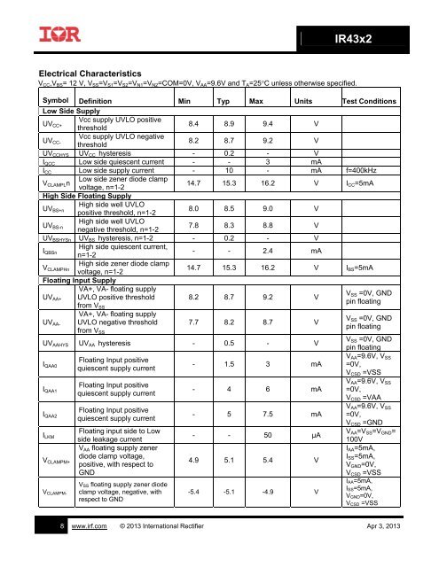
<strong>IR43x2</strong><br />
Electrical Characteristics<br />
VCC,VBS= 12 V, VSS=VS1=VS2=VN1=VN2=COM=0V, VAA=9.6V and TA=25C unless otherwise specified.<br />
Symbol Definition<br />
Low Side Supply<br />
UVCC+<br />
Vcc supply UVLO positive<br />
threshold<br />
UVCC-<br />
Vcc supply UVLO negative<br />
threshold<br />
Min<br />
Typ<br />
8 www.irf.com © 2013 <strong>International</strong> <strong>Rectifier</strong> Apr 3, 2013<br />
Max<br />
Units<br />
8.4 8.9 9.4 V<br />
8.2 8.7 9.2 V<br />
Test Conditions<br />
UVCCHYS UVCC hysteresis - 0.2 - V<br />
IQCC Low side quiescent current - - 3 mA<br />
ICC Low side supply current - 10 - mA f=400kHz<br />
VCLAMPLn<br />
Low side zener diode clamp<br />
voltage, n=1-2<br />
14.7 15.3 16.2 V ICC=5mA<br />
High Side Floating Supply<br />
UVBS+n<br />
High side well UVLO<br />
positive threshold, n=1-2<br />
8.0 8.5 9.0 V<br />
UVBS-n<br />
High side well UVLO<br />
negative threshold, n=1-2<br />
7.8 8.3 8.8 V<br />
UVBSHYSn UVBS hysteresis, n=1-2 - 0.2 - V<br />
IQBSn<br />
High side quiescent current,<br />
n=1-2<br />
- - 2.4 mA<br />
VCLAMPHn<br />
High side zener diode clamp<br />
voltage, n=1-2<br />
14.7 15.3 16.2 V IBS=5mA<br />
Floating Input Supply<br />
UVAA+<br />
UVAA-<br />
VA+, VA- floating supply<br />
UVLO positive threshold<br />
from VSS<br />
VA+, VA- floating supply<br />
UVLO negative threshold<br />
from VSS<br />
8.2 8.7 9.2 V<br />
7.7 8.2 8.7 V<br />
UVAAHYS UVAA hysteresis - 0.5 - V<br />
IQAA0<br />
IQAA1<br />
IQAA2<br />
ILKM<br />
VCLAMPM+<br />
VCLAMPM-<br />
Floating Input positive<br />
quiescent supply current<br />
Floating Input positive<br />
quiescent supply current<br />
Floating Input positive<br />
quiescent supply current<br />
Floating input side to Low<br />
side leakage current<br />
VAA floating supply zener<br />
diode clamp voltage,<br />
positive, with respect to<br />
GND<br />
VSS floating supply zener diode<br />
clamp voltage, negative, with<br />
respect to GND<br />
- 1.5 3 mA<br />
- 4 6 mA<br />
- 5 7.5 mA<br />
- - 50 µA<br />
4.9 5.1 5.4 V<br />
-5.4 -5.1 -4.9 V<br />
VSS =0V, GND<br />
pin floating<br />
VSS =0V, GND<br />
pin floating<br />
VSS =0V, GND<br />
pin floating<br />
VAA=9.6V, VSS<br />
=0V,<br />
VCSD =VSS<br />
VAA=9.6V, VSS<br />
=0V,<br />
VCSD =VAA<br />
VAA=9.6V, VSS<br />
=0V,<br />
VCSD =GND<br />
VAA=VSS=VGND=<br />
100V<br />
IAA=5mA,<br />
ISS=5mA,<br />
VGND=0V,<br />
VCSD =VSS<br />
IAA=5mA,<br />
ISS=5mA,<br />
VGND=0V,<br />
VCSD =VSS


