Functional Molecularly Imprinted Polymer Microstructures ...
Functional Molecularly Imprinted Polymer Microstructures ...
Functional Molecularly Imprinted Polymer Microstructures ...

You also want an ePaper? Increase the reach of your titles
YUMPU automatically turns print PDFs into web optimized ePapers that Google loves.
Experimental<br />
Chemicals: Vanadyl sulfate pentahydrate (purum, Fluka), TEOS (98 %, Fluka),<br />
hydrogen peroxide (30 %, Perhydrol, p.a., Merck), ammonia (25 %, p.a.,<br />
Merck), isopropanol (99.5 %, J. T. Baker) were used as purchased.<br />
Synthesis: Fibrous V3O7´H2O template crystals were prepared hydrothermally<br />
according to Yamamoto and co-workers [30]: an aqueous solution of<br />
VOSO4 (0.15 M) was sealed in a poly(tetrafluoroethylene)-lined autoclave<br />
(Parr bomb 4749, 23 mL capacity) and heated at 180±220 C for 1±2 days. The<br />
resulting suspension was filtered, washed several times with water and dried<br />
overnight under vacuum (~ 10 ±3 mbar). Coating of the as-prepared green, paper-like<br />
template as well as the subsequent core removal were performed in<br />
one pot. The fibrous solid (35 mg) was dispersed in a 250 mL glass flask containing<br />
an isopropanol/ammonia/water solution (respective volumes [mL]:<br />
200:8.3:7.5) by means of an ultrasonic bath set at 40 C (Bandelin SonorexDK<br />
255 P apparatus, 35 kHz, 320 W). After addition of 0.1 mL TEOS, the ultrasound<br />
intensity was maintained at ~ 200 W during the whole coating reaction<br />
(75 min). Then, 1 mL H 2O 2 was added directly into the dispersion, which was<br />
further stirred for about 45 min. The solid was collected by filtration, washed<br />
extensively with isopropanol, and afterwards with water. To achieve complete<br />
core dissolution as well as elemental purity, the product was redispersed in a diluted<br />
H2O2 aqueous solution (0.3 M; 30 mL), stirred for 48 h, washed several<br />
times with water, and dried under vacuum.<br />
Characterization: Samples were investigated in glass capillaries with a STOE<br />
STADI P X-ray powder diffractometer equipped with a curved Ge monochromator,<br />
a linear position sensitive detector, and using Cu Ka radiation. Scanning<br />
electron microscopy (SEM) was performed on a LEO 1530 Gemini apparatus,<br />
which was operated at low acceleration voltage (Vacc = 1 kV) to minimize charging<br />
of the as-synthesized samples. For transmission electron microscopy (TEM),<br />
the samples were deposited on a holey carbon foil supported on a copper grid.<br />
TEM images were recorded on a CM30 microscope (Philips, Eindhoven,<br />
V acc = 300 kV, LaB 6 cathode). Elemental maps of vanadium were obtained at<br />
the L ionization edge applying the three-window method [33] on a Tecnai 30F<br />
apparatus (Philips, Eindhoven, V acc = 300 kV, field emission gun) equipped with<br />
a GIF (Gatan imaging filter). Laser elemental analysis was carried out on a<br />
pressed sample pellet using a Perkin Elmer/SciexElan 6100 DRC LA-ICP-MS<br />
machine.<br />
Received: March 20, 2003<br />
Final version: June 5, 2003<br />
± [1] S. Iijima, Nature 1991, 354, 56.<br />
[2] W. Tremel, Angew. Chem. Int. Ed. 1999, 38, 2175.<br />
[3] R. Tenne, Prog. Inorg. Chem. 2001, 50, 269.<br />
[4] G. R. Patzke, F. Krumeich, R. Nesper, Angew. Chem. Int. Ed. 2002, 41,<br />
2446.<br />
[5] Y. Konishi, M. Okazaki, K. Toriyama, T. Kasai, J. Phys. Chem. B 2001,<br />
105, 9101.<br />
[6] J. L. Gole, M. G. White, J. Catal. 2001, 204, 249.<br />
[7] A. Hanprasopwattana, S. Srinivasan, A. G. Sault, A. K. Datye, Langmuir<br />
1996, 12, 3173.<br />
[8] M. Quobosheane, S. Santra, P. Zhang, W. Tan, Analyst 2001, 126, 1274.<br />
[9] J. Livage, T. Coradin, C. Roux, J. Phys.: Condens. Matter 2001, 13, R673.<br />
[10] T. K. Jain, I. Roy, T. K. De, A. Maitra, J. Am. Chem. Soc. 1998, 120,<br />
11 092.<br />
[11] H. J. Chang, Y. F. Chen, H. P. Lin, C. Y. Mou, Appl. Phys. Lett. 2001, 78,<br />
3791.<br />
[12] M. Zhang, E. Ciocan, Y. Bando, K. Wada, L. L. Cheng, P. Pirouz, Appl.<br />
Phys. Lett. 2002, 80, 491.<br />
[13] L. L. Hench, J. K. West, Chem. Rev. 1990, 90, 33.<br />
[14] R. A. Caruso, M. Antonietti, Chem. Mater. 2001, 13, 3272.<br />
[15] J. H. Jung, Y. Ono, S. Shinkai, Langmuir 2000, 16, 1643.<br />
[16] F. Kleitz, U. Wilczok, F. Schüth, F. Marlow, Phys. Chem. Chem. Phys.<br />
2001, 3, 3486.<br />
[17] S. M. Yang, I. Sokolov, N. Coombs, C. T. Kresge, G. A. Ozin, Adv. Mater.<br />
1999, 11, 1427.<br />
[18] S. Baral, P. Schoen, Chem. Mater. 1993, 5, 145.<br />
[19] Y. Ono, Y. Kanekiyo, K. Inoue, J. Hojo, M. Nango, S. Shinkai, Chem. Lett.<br />
1999, 475.<br />
[20] W. Shenton, T. Douglas, M. Young, G. Stubbs, S. Mann, Adv. Mater. 1999,<br />
11, 253.<br />
[21] H. Nakamura, Y. Matsui, J. Am. Chem. Soc. 1995, 117, 2651.<br />
[22] F. Miyaji, S. A. Davis, J. P. H. Charmant, S. Mann, Chem. Mater. 1999, 11,<br />
3021.<br />
[23] L. Wang, S. Tomura, F. Ohashi, M. Maeda, M. Suzuki, K. Inukai, J. Mater.<br />
Chem. 2001, 11, 1465.<br />
[24] B. C. Satishkumar, A. Govindaraj, E. M. Vogl, L. Basumallick, C. N. R.<br />
Rao, J. Mater. Res. 1997, 12, 604.<br />
[25] C. R. Martin, Science 1994, 266, 1961.<br />
[26] B. B. Lakshmi, C. J. Patrissi, C. R. Martin, Chem. Mater. 1997, 9, 2544.<br />
[27] F. Schlottig, M. Textor, U. Georgi, G. Roewer, J. Mater. Sci. Lett. 1999, 18,<br />
599.<br />
[28] M. Zhang, Y. Bando, K. Wada, J. Mater. Res. 2000, 15, 387.<br />
[29] C. Hippe, M. Wark, E. Lork, G. Schulz-Ekloff, Microporous Mesoporous<br />
Mater. 1999, 31, 235.<br />
[30] Y. Oka, T. Yao, N. Yamamoto, J. Solid State Chem. 1990, 89, 372.<br />
[31] Joint Committee on Powder Diffraction Standards (JCPDS), International<br />
Centre for Diffraction Data (ICDD), card No. 28±1433<br />
(V3O7´H2O).<br />
[32] W. Stöber, A. Fink, E. Bohn, J. Colloid Interface Sci. 1968, 26,62.<br />
[33] L. Reimer, Energy-Filtering Transmission Electron Microscopy, Springer,<br />
Berlin 1995, p. 347.<br />
<strong>Functional</strong> <strong>Molecularly</strong> <strong>Imprinted</strong> <strong>Polymer</strong><br />
<strong>Microstructures</strong> Fabricated Using<br />
Microstereolithography**<br />
By Peter G. Conrad II, Peter T. Nishimura, Damian Aherne,<br />
Benjamin J. Schwartz, Dongmin Wu, Nicholas Fang,<br />
Xiang Zhang, M. Joseph Roberts, and Kenneth J. Shea*<br />
A defining trend in sensing and diagnostics is miniaturization,<br />
the reduction in the size of devices and components to<br />
micrometer or submicrometer length scales. [1±4] More compact<br />
devices have lower power demands and the potential for<br />
a greater economy of production. Applications for micro-devices<br />
are numerous and include implantable medical biosensors,<br />
[5±11] drug-screening devices, [12] and microelectromechanical<br />
systems (MEMS). [1,13±15] Microfabrication technology can<br />
achieve rapid assembly of the electrical and mechanical components<br />
of these devices. However, the introduction of additional<br />
function, such as molecular recognition to identify or<br />
concentrate biological analytes, requires ªsoftº materials.<br />
These ªsoftº materials are typically not compatible with direct<br />
lithographic techniques and thus their introduction is<br />
achieved in subsequent steps of device fabrication. In addition<br />
to the obvious advantages of simplification of the fabrication<br />
process, compatible functionalization procedures could<br />
±<br />
[*] Prof. K. J. Shea, Dr. P. G. Conrad II<br />
Department of Chemistry, University of California<br />
Irvine, CA 92697-2025 (USA)<br />
E-mail: KJShea@uci.edu<br />
Dr. P. T. Nishimura, Dr. D. Aherne, Prof. B. J. Schwartz<br />
Department of Chemistry and Biochemistry, University of California<br />
Los Angeles, CA 90095-1569 (USA)<br />
Dr. D. Wu, Dr. N. Fang, Prof. X. Zhang,<br />
Department of Mechanical and Aerospace Engineering<br />
University of California<br />
Los Angeles, CA 90095-1569 (USA<br />
Dr. M. J. Roberts<br />
NAVAIR NAWCWD, <strong>Polymer</strong> Science and Engineering Branch<br />
China Lake, CA 93555 (USA)<br />
[**] The authors are grateful to DARPA for financial support. Research in the<br />
KJS lab is partially supported by the National Institute of Health. BJS is a<br />
Cottrell Scholar of Research Corporation, an Alfred P. Sloan Foundation<br />
Research Fellow, and a Camille Dreyfus Teacher-Scholar. Microstereolithography<br />
work at the XZ lab is partially funded by NSF CAREER<br />
Award and ONR Young Investigator Award.<br />
Adv. Mater. 2003, 15, No. 18, September 16 DOI: 10.1002/adma.200304602 Ó 2003 WILEY-VCH Verlag GmbH & Co. KGaA, Weinheim 1541<br />
COMMUNICATIONS
COMMUNICATIONS<br />
further expand the utility and scope of micro devices. For a<br />
lithographic approach, this would require methods to produce<br />
spatially resolved, micrometer-sized features of functional<br />
materials capable of molecular recognition.<br />
Of the many strategies for creating synthetic receptors,<br />
molecular imprinting, a method for making robust crosslinked<br />
polymers with recognition sites for complexorganic molecules,<br />
offers a number of advantages for this application. [16±20]<br />
<strong>Molecularly</strong> imprinted polymers (MIPs) are typically thermosets<br />
generated by polymerization of fluid solutions of monomers.<br />
Importantly, the approach is generally offering the<br />
opportunity for fabricating receptors for a variety of molecular<br />
structures. Furthermore, the imprinted photopolymers<br />
containing recognition sites are capable of withstanding a<br />
variety of solvents and temperature extremes. [16±20] The integration<br />
of imprinted polymers into micro-sensors and diagnostic<br />
devices requires procedures for fabricating MIPs in<br />
two- and three-dimensional (2D and 3D) patterns. Methods<br />
for producing these structures include simple lithography,<br />
microcontact printing (soft lithography), [21±23] microstereolithography<br />
(lSL), and 2-photon-3D lithography. [24] There<br />
have been very few reports of micropatterned functional<br />
MIPs. A notable exception is the work of Yan and Kapua,<br />
who reported fabrication of imprinted micrometer-sized features<br />
using soft lithography. [21]<br />
In this communication, we report the use of lSL for fabricating<br />
imprinted 3D microstructures capable of recognizing a<br />
targeted analyte. The imprinting procedure should, with some<br />
modification, be applicable to many standard lithographic<br />
methods.<br />
lSL is a method for manufacturing complex3D shapes by<br />
means of localized photopolymerization using a sharply<br />
focused laser beam. [25] lSL was first reported in 1993 utilizing<br />
principles based on stereolithography to fabricate macro-sized<br />
O<br />
OH +<br />
MAA, 2<br />
N<br />
N<br />
9-DA , 5<br />
H H<br />
N<br />
N<br />
H H<br />
N<br />
N<br />
N<br />
N<br />
SO2 N<br />
N<br />
9-EA, 1<br />
O<br />
O<br />
TRIM 4<br />
BEE 3 Tinuvin 6<br />
CHCl3<br />
O<br />
O H<br />
H H<br />
N<br />
N<br />
N<br />
3<br />
N<br />
N<br />
O2S<br />
O<br />
O<br />
H<br />
models. [26] A computer-assisted design (CAD) program is<br />
used to horizontally slice the desired 3D image into 2D layers.<br />
A directed UV laser beam is focused to 1±2 lm onto the surface<br />
of a glass microscope slide coated with a thin layer of a<br />
liquid monomer solution, resulting in localized photopolymerization;<br />
synchronized motion of the substrate in the x±y plane<br />
is then used to fabricate the pattern of the lowest 2D<br />
slice. [25,27] Translation along the z-axis allows the next layer to<br />
be ªwrittenº on top of the first. Repetition of these steps<br />
allows complexand intricate microstructures to be built layer<br />
by layer.<br />
To achieve spatial resolution, it is necessary to control the<br />
effective area of localized photopolymeriztion, which determines<br />
the height, or ªcuring depthº, of each of the polymerized<br />
layers. Jacobs [28] established a working curve for controlling<br />
the curing depth in lSL based on the photopolymer's<br />
threshold exposure. The curing depth (Cd) depends, in part,<br />
on the concentration and molar extinction coefficients of the<br />
initiator and an additional UV-absorber (UVA).<br />
For the integration of lSL and imprinting we elected to fabricate<br />
well-defined, micrometer-sized structures with adenine<br />
recognition. [29] Adenine was chosen because of the occurrence<br />
of this fragment in many biologically important molecules and<br />
the considerable information available regarding the preparation<br />
and evaluation of molecularly imprinted synthetic adenine<br />
receptors. [29±31] An imprinting formulation developed for<br />
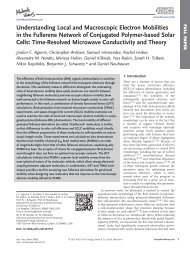
lSL is shown in Figure 1. The components include 9-ethyl<br />
adenine (9-EA, 1, the imprint molecule) and methacrylic acid<br />
(MAA, 2, the functional monomer) in concentrated chloroform<br />
solution. [30] The high degree of crosslinking, a requirement<br />
for imprinting, [32] was achieved by incorporation of the<br />
trifunctional crosslinker trimethylolpropane trimethacrylate<br />
(TRIM, 4). The choice of photoinitiator and UVA additive<br />
was dictated by absorption wavelength, quantum efficiency,<br />
O<br />
O<br />
H H<br />
O N O<br />
H<br />
H<br />
N<br />
N<br />
N N<br />
1542 Ó 2003 WILEY-VCH Verlag GmbH & Co. KGaA, Weinheim http://www.advmat.de Adv. Mater. 2003, 15, No. 18, September 16<br />
- 9-EA, 1<br />
O<br />
BEE, 3<br />
OEt<br />
O<br />
O H<br />
HO<br />
N<br />
N<br />
N<br />
Tinuvin, 6<br />
Fig. 1. Scheme depicting the fabrication of adenine selective molecularly imprinted polymers and subsequent absorption of the adenine derivative,<br />
9-dansyl adenine, 5. 9-Ethyl adenine, 1, serves as the template with methacrylic acid, 2, as the functional monomer, while TRIM, 4, functions as a<br />
crosslinking agent. Benzoin ethyl ether, 3, is utilized as the initiator for lSL procedures, and Tinuvin, 6, is added as a UVA to achieve curing depth resolution.<br />
9-Dansyl adenine, 5, functions as a fluorescent probe to analyze the binding sites in the resulting microstructure.<br />
O<br />
O<br />
H<br />
Ph<br />
Ph
and compatibility with the formation of a functional MIP.<br />
After considerable experimentation (vide infra), benzoin<br />
ethyl ether (BEE, 3, k = 354 nm (e = 509 M ±1 cm ±1 )), and Tinuvin,<br />
6, were chosen as the photoinitiator and the UVA<br />
additive, respectively. Tinuvin (6) possesses a large molar absorptivity<br />
coefficient (151 600 M ±1 cm ±1 ) at 364 nm (the photopolymerization<br />
wavelength employed) and was found to be<br />
effective in achieving low curing depths (high z spatial resolution).<br />
The evaluation of imprinted polymers prepared by bulk<br />
polymerization is traditionally conducted using high-pressure<br />
liquid chromatography (HPLC) techniques. However, with<br />
micrometer-sized objects, the number of binding sites is below<br />
the detection limits of HPLC analysis. We have developed an<br />
assay that utilizes the fluorescence emission of a dansyltagged<br />
adenine derivative to evaluate binding to microfabricated<br />
structures. <strong>Polymer</strong>s imprinted with 9-EA display an<br />
affinity for a number of adenine derivatives bearing substituents<br />
at the 9-position. [29±31] The adenine specificity is not compromised<br />
by these substituents. The primary binding interactions<br />
between adenine derivatives and the carboxylic acid<br />
functional groups on the imprinted polymer are believed to<br />
be Watson±Crick and Hoogstein H-bonding interactions on<br />
the basic residues of the ªupper portionº of the adenine molecule.<br />
[30] These recognition elements allow considerable freedom<br />
in substitution at the 9-position (ªlower portionº) while<br />
maintaining overall adenine specificity by the MIP. A fluorescent<br />
analog, 9-dansyl adenine (9-DA, 5), was synthesized<br />
for this purpose. [33] Independent evaluation of the affinity of<br />
9-EA imprinted polymers towards 9-DA was established in<br />
bulk polymer experiments.<br />
To verify that the choice of 3 as a photoinitiator and 6 as a<br />
UVA does not interfere with the imprinting process or create<br />
additional non-specific binding interactions, a variety of nonpatterned<br />
test samples were prepared. Their composition is<br />
summarized in Table 1. Each of the four solution mixtures<br />
(S1±S4) was dip-coated onto glass microscope slides previously<br />
silylated with 3-(trimethyoxysilyl)propyl methacrylate,<br />
allowing for better adhesion of the photodeposited polymer<br />
to the glass substrates.<br />
The polymers were grown by light exposure in a UV-chamber<br />
for 5 min then washed in chloroform for 12 h to remove<br />
9-EA, 6, 3, and any unreacted monomers. The washing proto-<br />
Table 1. Composition of solutions used during polymerization procedures.<br />
Chloroform and TRIM were purified by flashing through an alumina column,<br />
while 9-ethyl adenine was flash chromatographed on a silica column.<br />
Methacrylic acid was freshly distilled prior to use. Tinuvin and benzoin ethyl<br />
ether were used as received. Solutions were prepared freshly prior to use, and<br />
stored in an amber bottle to keep from incident light.<br />
Substrate S1 S2 S3 S4<br />
Chloroform 6.271 g 6.271 g 6.271 g 6.271 g<br />
TRIM 6.274 g 6.274 g 6.274 g 6.274 g<br />
Methacrylic acid 0.327 g 0.327 g 0.327 g 0.327 g<br />
Tinuvin 0.013 g ± 0.013 g ±<br />
Benzoin ethyl ether 0.131 g 0.131 g 0.131 g 0.131 g<br />
9-Ethyl adenine 0.050 g 0.050 g ± ±<br />
col of these non-covalent imprinted polymers has been shown<br />
to quantitatively remove template molecules. [29±31] These unpatterned<br />
samples were then bathed in a 1 ” 10 ±5 M solution<br />
of 9-DA in chloroform. The 9-DA absorbed in the samples<br />
was excited using the 488 nm line from an Ar + laser (a wavelength<br />
chosen to avoid absorption by any residual 6), and<br />
~ 600 nm dansyl fluorescence from the samples was imaged<br />
through a 530 nm long pass filter onto a charge coupled device<br />
(CCD) camera. Integration of the fluorescent image was<br />
plotted as a function of time and demonstrates that the additional<br />
reagents required for lSL do not interfere with the<br />
binding interactions between functional monomer and template<br />
during the polymerization process. Additionally, the<br />
reagents do not provide an increase in non-specific binding<br />
sites.<br />
Having established imprinting formulations for patterning<br />
we next devoted our attention to the micropatterning of functional<br />
polymers via lSL. First, 2D patterns were fabricated to<br />
verify that the patterned microstructures show similar selectivity<br />
to the bulk polymers. 2D grids were prepared from the<br />
UV-curable MIP and control UV-curable solutions (S1 and<br />
S3, respectively) using the 364 nm line of the Ar + laser and an<br />
x±y±z motorized stage. Figure 2 shows an image of the resulting<br />
pattern, which has an overall dimension of 600 lm<br />
” 600 lm; the width of the lines comprising the grid is<br />
COMMUNICATIONS<br />
pleted. After building up multiple 2D layers, the resulting 3D<br />
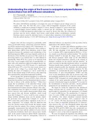
polymer objects had a total height of approximately 100 lm;<br />
scanning electron micrographs of the 3D ªwaffle patternº produced<br />
in this fashion are shown in Figure 3.<br />
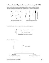
As with the unpatterned and 2D patterned polymers, rebinding<br />
studies were conducted for both the MIP and control<br />
3D structures. The 3D structures were rinsed and bathed in<br />
chloroform for 12 h to wash the 9-EA template and any<br />
unreacted materials from the MIP. The structures were then<br />
exposed to a solution of 9-DA (1.08 ” 10 ±4 M in chloroform)<br />
for increasing time intervals, gently rinsed to remove any<br />
residual 9-DA, and fluorescently imaged. The results are<br />
shown in Figure 4.<br />
An approximate 4.5-fold increase in fluorescent intensity<br />
compared to the control polymer S3 was observed in the imprinted<br />
structure S1. These results indicate that the 3D microstructures<br />
exhibit affinity for 9-DA comparable to that of the<br />
2D and bulk imprinted materials.<br />
In summary, we have demonstrated the ability to fabricate<br />
functionalized, three-dimensional molecularly imprinted microstructures<br />
using lSL. <strong>Microstructures</strong> with recognition for<br />
adenine and its derivatives have been prepared. The experimental<br />
conditions used to achieve spatial resolution in lSL do<br />
not disrupt the binding interactions between the functional<br />
monomers and the template. The range of target analytes that<br />
are responsive to molecular imprinting is large and includes<br />
simple drugs and their metabolites, pesticides, peptides, and<br />
proteins. These techniques will allow for the direct integration<br />
of functional polymers with molecular recognition into the<br />
microfabrication process.<br />
Received: November 11, 2002<br />
Final version: June 10, 2003<br />
±<br />
[1] R. Mariella Jr., Biomed. Microdevices 2002, 4, 77.<br />
[2] M. J. O'Donnell-Maloney, D. P. Little, Genet. Anal.: Biomol. Eng. 1996,<br />
13, 151.<br />
[3] J. Wang, F. Lu, L. Angnes, J. Liu, H. Sakslund, Q. Chen, M. Pedrero,<br />
L. Chen, O. Hammerich, Anal. Chim. Acta 1995, 305, 3.<br />
[4] W. E. Morf, N. F. de Rooij, Sens. Actuators, A 1995, A51, 89.<br />
[5] Z. A. Strong, A. W. Wang, C. F. McConaghy, Biomed. Microdevices 2002,<br />
4,97.<br />
[6] R. Hintsche, M. Paeschke, U. Wollenberger, U. Schnakenberg, B. Wagner,<br />
T. Lisec, Biosens. Bioelectron. 1994, 9, 697.<br />
[7] L. Tiefenauer, C. Padeste, Chimia 1999, 53, 62.<br />
[8] O. Niwa, K. Hayashi, R. Kurita, T. Horiuchi, Mater. Integr. 2002, 15, 17.<br />
(a) (b)<br />
0<br />
0 10 20 30 40 50 60 70<br />
[9] S. Shoji, T. Ohori, H. Kawashima, K. Miura, A. Yotsumoto, Proc.ÐElectrochem.<br />
Soc. 1997, 97-5, 12.<br />
[10] B. Xie, K. Ramanathan, B. Danielsson, TrAC, Trends Anal. Chem. 2000,<br />
19, 340.<br />
[11] K. Hayashi, R. Kurita, T. Horiuchi, O. Niwa, Chem. Sens. 2001, 17,97.<br />
[12] Y. Jiang, P. Wang, L. E. Locascio, C. S. Lee, Anal. Chem. 2001, 73, 2048.<br />
[13] C. J. H. Brenan, K. Domansky, P. Kurzawski, L. G. Griffith, Proc. SPIEÐ<br />
Int. Soc. Opt. Eng. 2000, 3912, 76.<br />
[14] C. B. Freidhoff, R. M. Young, S. Sriram, T. T. Braggins, T. W. O'Keefe,<br />
J. D. Adam, H. C. Nathanson, R. R. A. Syms, T. J. Tate, M. M. Ahmad, S.<br />
Taylor, J. Tunstall, J. Vac. Sci. Technol., A 1999, 17, 2300.<br />
[15] C.-F. Yeh, Y.-C. Lee, J.-L. Su, Proc. SPIEÐInt. Soc. Opt. Eng. 1996, 2879,<br />
260.<br />
[16] G. Wulff, Angew. Chem., Int. Ed. Engl. 1995, 34, 1812.<br />
[17] K. J. Shea, Trends Polym. Sci. 1994, 2, 166.<br />
[18] M. J. Whitecombe, E. N. Vulfson, Adv. Mater. 2001, 13,467.<br />
[19] K. Haupt and K. Mosbach, Chem. Rev. 2000, 100, 2495.<br />
[20] B. Sellergren, <strong>Molecularly</strong> <strong>Imprinted</strong> <strong>Polymer</strong>s: Man-Made Mimics of Antibodies<br />
and Their Applications in Analytical Chemistry, Vol. 23, Elsevier,<br />
New York 2001.<br />
[21] M. Yan, A. Kapua, Anal. Chim. Acta 2001, 435, 163.<br />
[22] G. M. Whitesides, E. Ostuni, S. Takayama, X. Jiang, D. E. Ingber, Annu.<br />
Rev. Biomed. Eng. 2001, 3, 335.<br />
[23] G. Vozzi, C. J. Flaim, F. Bianchi, A. Ahluwalia, S. Bhatia, Mater. Sci. Eng.,<br />
C 2002, 20, 43.<br />
[24] X. Zhang, X. N. Jiang, C. Sun, Sens. Actuators, A 1999, 77,149.<br />
[25] S. Kawata, H. B. Sun, T. Tanaka, K. Takada, Nature 2001, 412, 697.<br />
[26] K. Ikuta, K. Hirowatari, Proc.ÐIEEE Micro Electro Mech. Syst. 1993,42.<br />
[27] C. Sun, X. Zhang, J. Appl. Phys. 2002, 92, 4796.<br />
[28] P. F. Jacobs, Rapid Prototyping and Manufacturing: Fundamentals of<br />
Stereolithography, Society of Manufacuring Engineers, Dearborn, MI<br />
1992.<br />
[29] K. J. Shea, D. A. Spivak, B. Sellergren, J. Am. Chem. Soc. 1993, 115, 3368.<br />
[30] D. A. Spivak, M. A. Gilmore, K. J. Shea, J. Am. Chem. Soc. 1997, 119,<br />
4388.<br />
[31] D. A. Spivak, K. J. Shea, Macromolecules 1998, 31, 2160.<br />
[32] A. Guyot, M. Bartholin, Prog. Polym. Sci. 1982, 8, 227.<br />
[33] Synthetic Procedures in Nucleic Acid Chemistry, Vol. 1, 2 (Eds: W. W. Zorbach,<br />
R. S. Tipson), Interscience, New York 1968.<br />
1544 Ó 2003 WILEY-VCH Verlag GmbH & Co. KGaA, Weinheim http://www.advmat.de Adv. Mater. 2003, 15, No. 18, September 16<br />
5<br />
4<br />
3<br />
2<br />
1<br />
Blank<br />
Fig. 4. Rebinding isotherm (fluorescence intensity as a function of exposure<br />
time to a 1.08 ” 10 ±4 M solution of 9-DA in chloroform) for both 9-EA-imprinted<br />
(MIP) and control (blank) 3D microstructures as those presented in<br />
Figure 3.<br />
Fig. 3. a) SEM image of a 3D imprinted microstructure (600 lm ” 600 lm ” 100 lm). b) Close-ups of the structure show the wall thickness to be<br />
approximately 10 lm.<br />
MIP