You also want an ePaper? Increase the reach of your titles
YUMPU automatically turns print PDFs into web optimized ePapers that Google loves.
<strong>Moving</strong> <strong>to</strong> <strong>Altium</strong> <strong>Designer</strong> <strong>From</strong> OrCAD<br />
Project hierarchy<br />
For any project involving multi-sheet design, there are basically two choices that need <strong>to</strong> be made –<br />
defining the structural relationship between the schematic sheets (flat or hierarchical), and determining<br />
the method of electrical connectivity between the circuitry on those sheets. Display of the project<br />
hierarchy in <strong>Altium</strong> <strong>Designer</strong>’s Projects panel is quite similar <strong>to</strong> OrCAD Capture’s Project Manager,<br />
with some differences in naming conventions and how hierarchies are graphically represented.<br />
Defining your sheet structure in OrCAD Capture’s Project Manager<br />
Like <strong>Altium</strong> <strong>Designer</strong>, Capture supports flat and hierarchical designs. Both use a block-like symbol <strong>to</strong><br />
define sheet-<strong>to</strong>-sheet structure in a hierarchical design, called a Sheet Symbol in <strong>Altium</strong> <strong>Designer</strong>, and<br />
a Hierarchical Block in Capture. In both the symbol references the lower level schematic. In <strong>Altium</strong><br />
<strong>Designer</strong> this is simply another schematic sheet, in Capture it can be more complex.<br />
Capture has another layer of design partitioning that affects hierarchy. In Capture there is a schematic,<br />
which present as a folder icon in Capture’s Project Manager, and there are pages, which present as a<br />
schematic sheet icon. Each Capture schematic can be made up of one or more pages. The Capture<br />
hierarchical block points <strong>to</strong> the schematic below, which means the block can actually reference circuitry<br />
divided over multiple pages.<br />
Typically a flat Capture design is one schematic (folder),<br />
with the design being drawn on as many pages as required<br />
in that schematic (folder). For a hierarchical design, the<br />
hierarchical block symbol (or part with an attached<br />
schematic sheet or model) is the mechanism used <strong>to</strong><br />
partition the major functional regions of a design.<br />
For a simple hierarchy, each hierarchical block, or part with<br />
an attached schematic folder, or VHDL model, represents a<br />
unique design module. The Hierarchy tab in OrCAD<br />
Capture’s Project Manager displays a simple hierarchical<br />
design as a tree of schematic pages. The schematic folder<br />
or VHDL entity at the <strong>to</strong>p of a hierarchy, which directly or<br />
indirectly refers <strong>to</strong> all other modules in the design, is called<br />
the root module. In the OrCAD Project Manager's File tab,<br />
the root module has a backslash on its folder icon (Figure<br />
7). The root module folder, as well as any other module<br />
folder, can contain as many schematic pages or VHDL<br />
models as required.<br />
Now let’s look at <strong>Altium</strong> <strong>Designer</strong>.<br />
Sheet structure in <strong>Altium</strong> <strong>Designer</strong>’s Projects panel<br />
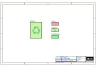
Figure 7. The structure of an example<br />
CPU_Design project as it would appear in<br />
OrCAD Capture.<br />
In <strong>Altium</strong> <strong>Designer</strong>, hierarchical designs can likewise be viewed and navigated also as a tree structure<br />
through the Projects panels. Once the project has been compiled at least once, the Projects panel will<br />
show the hierarchical structure. In a hierarchical design you can think of the first sheet as the parent<br />
and those represented by sheet symbols as children (note that child sheets can have their own children<br />
<strong>to</strong>o). With that idea in mind, the tree view of the hierarchy makes it easy <strong>to</strong> navigate and get the overall<br />
8 AP0132 (v2.1) February 21, 2006