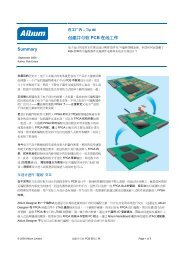
Create successful ePaper yourself
Turn your PDF publications into a flip-book with our unique Google optimized e-Paper software.
Board Layers and Colors<br />
<strong>Moving</strong> <strong>to</strong> <strong>Altium</strong> <strong>Designer</strong> <strong>From</strong> OrCAD<br />
Select Design » Board Layers and Colors [shortcut L] from the main menu command <strong>to</strong> display this<br />
dialog where you can display, add, remove, rename, and set the colors of the layers. It’s worth<br />
mentioning that you can easily navigate between the layers of your design simply by selecting the layer<br />
tabs at the bot<strong>to</strong>m of the main design window.<br />
Layer Stack Manager<br />
Layers can be easily managed and seen with the Layer Stack Manager. This dialog is easily accessed<br />
again from the main command menu Design » Layer Stack Manager [shortcut D, K]. Some other<br />
helpful shortcut keys from the numeric keypad include the ‘+’ and ‘–‘for cycling through all visible<br />
layers, and the ‘ * ‘<strong>to</strong> cycle through visible signal layers.<br />
For further information on setting up your board, refer <strong>to</strong> the tu<strong>to</strong>rial Preparing the Board for Design<br />
Transfer.<br />
Design Rules<br />
The PCB Edi<strong>to</strong>r is a powerful and dynamic rules-driven environment. This means that as you work in<br />
the PCB Edi<strong>to</strong>r and do things that change the design (such as placing tracks, moving components, or<br />
routing the board), the PCB Edi<strong>to</strong>r constantly moni<strong>to</strong>rs each action and checks <strong>to</strong> see if the design still<br />
complies with the design rules. If it doesn’t, an error is immediately flagged for your attention.<br />
With the PCB as the active document, select Design » Rules from the main command menu <strong>to</strong> invoke<br />
the PCB Rules and Constraint Edi<strong>to</strong>r dialog as shown below in Figure 12.<br />
Figure 12. The PCB Rules and Constraint Edi<strong>to</strong>r where all design rules can be managed.<br />
AP0132 (v2.1) February 21, 2006 17