MCP2561/2 Data Sheet - Semitron
MCP2561/2 Data Sheet - Semitron
MCP2561/2 Data Sheet - Semitron

Create successful ePaper yourself
Turn your PDF publications into a flip-book with our unique Google optimized e-Paper software.
Features:<br />
• Supports 1 Mb/s Operation<br />
• Implements ISO-11898-5 Standard Physical Layer<br />
Requirements<br />
• Very Low Standby Current (5 µA, typical)<br />
• VIO Supply Pin to Interface Directly to<br />
CAN Controllers and Microcontrollers with<br />
1.8V to 5.5V I/O<br />
• SPLIT Output Pin to Stabilize Common Mode in<br />
Biased Split Termination Schemes<br />
• CAN Bus Pins are Disconnected when Device is<br />
Unpowered<br />
- An Unpowered Node or Brown-Out Event will<br />
Not Load the CAN Bus<br />
• Detection of Ground Fault:<br />
- Permanent Dominant Detection on TXD<br />
- Permanent Dominant Detection on Bus<br />
• Power-on Reset and Voltage Brown-Out<br />
Protection on VDD and VIO Pin<br />
• Protection Against Damage Due to Short-Circuit<br />
Conditions (Positive or Negative Battery Voltage)<br />
• Protection Against High-Voltage Transients in<br />
Automotive Environments<br />
• Automatic Thermal Shutdown Protection<br />
• Suitable for 12V and 24V Systems<br />
• Meets or exceeds stringent automotive design<br />
requirements including “Hardware Requirements<br />
for LIN, CAN and FlexRay Interfaces in Automotive<br />
Applications”, Version 1.3, May 2012<br />
• High-Noise Immunity Due to Differential Bus<br />
Implementation<br />
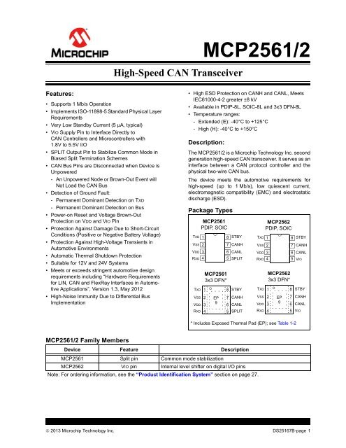
<strong>MCP2561</strong>/2 Family Members<br />
High-Speed CAN Transceiver<br />
<strong>MCP2561</strong>/2<br />
• High ESD Protection on CANH and CANL, Meets<br />
IEC61000-4-2 greater ±8 kV<br />
• Available in PDIP-8L, SOIC-8L and 3x3 DFN-8L<br />
• Temperature ranges:<br />
- Extended (E): -40°C to +125°C<br />
- High (H): -40°C to +150°C<br />
Description:<br />
The <strong>MCP2561</strong>/2 is a Microchip Technology Inc. second<br />
generation high-speed CAN transceiver. It serves as an<br />
interface between a CAN protocol controller and the<br />
physical two-wire CAN bus.<br />
The device meets the automotive requirements for<br />
high-speed (up to 1 Mb/s), low quiescent current,<br />
electromagnetic compatibility (EMC) and electrostatic<br />
discharge (ESD).<br />
Package Types<br />
TXD 1<br />
VSS 2<br />
VDD 3<br />
RXD 4<br />
<strong>MCP2561</strong><br />
PDIP, SOIC<br />
TXD 1<br />
VSS 2<br />
VDD 3<br />
RXD 4<br />
7 CANH<br />
6 CANL<br />
5 SPLIT<br />
TXD 1<br />
VSS 2<br />
VDD 3<br />
RXD 4<br />
MCP2562<br />
PDIP, SOIC<br />
7 CANH<br />
6 CANL<br />
5 VIO<br />
2013 Microchip Technology Inc. DS25167B-page 1<br />
8<br />
<strong>MCP2561</strong><br />
3x3 DFN*<br />
EP<br />
9<br />
8<br />
STBY<br />
STBY<br />
7 CANH<br />
6 CANL<br />
5 SPLIT<br />
TXD 1<br />
VSS 2<br />
VDD 3<br />
RXD 4<br />
MCP2562<br />
3x3 DFN*<br />
* Includes Exposed Thermal Pad (EP); see Table 1-2<br />
Device Feature Description<br />
<strong>MCP2561</strong> Split pin Common mode stabilization<br />
MCP2562 VIO pin Internal level shifter on digital I/O pins<br />
Note: For ordering information, see the “Product Identification System” section on page 27.<br />
EP<br />
9<br />
8<br />
8<br />
STBY<br />
STBY<br />
7 CANH<br />
6 CANL<br />
5 VIO
<strong>MCP2561</strong>/2<br />
Block Diagram<br />
TXD<br />
STBY<br />
RXD<br />
(2 )<br />
SPLIT<br />
VDD/2<br />
VIO<br />
VIO<br />
VIO (3)<br />
Digital I/O<br />
Supply<br />
Permanent<br />
Dominant Detect<br />
Mode<br />
Control<br />
Wake-Up<br />
Filter<br />
Receiver<br />
Thermal<br />
Protection<br />
Driver<br />
and<br />
Slope Control<br />
LP_RX (1)<br />
HS_RX<br />
POR<br />
UVLO<br />
CANH<br />
CANL<br />
CANH<br />
CANL<br />
Note 1: There is only one receiver implemented. The receiver can operate in Low-Power or High-Speed mode.<br />
2: Only <strong>MCP2561</strong> has the SPLIT pin.<br />
3: Only MCP2562 has the VIO pin. In <strong>MCP2561</strong>, the supply for the digital I/O is internally connected to VDD.<br />
DS25167B-page 2 2013 Microchip Technology Inc.<br />
VDD<br />
VSS<br />
CANH<br />
CANL
1.0 DEVICE OVERVIEW<br />
The <strong>MCP2561</strong>/2 is a high-speed CAN, fault-tolerant<br />
device that serves as the interface between a CAN<br />
protocol controller and the physical bus. The<br />
<strong>MCP2561</strong>/2 device provides differential transmit and<br />
receive capability for the CAN protocol controller, and<br />
is fully compatible with the ISO-11898-5 standard. It will<br />
operate at speeds of up to 1 Mb/s.<br />
Typically, each node in a CAN system must have a<br />
device to convert the digital signals generated by a<br />
CAN controller to signals suitable for transmission over<br />
the bus cabling (differential output). It also provides a<br />
buffer between the CAN controller and the high-voltage<br />
spikes that can be generated on the CAN bus by<br />
outside sources.<br />
TABLE 1-1: MODES OF OPERATION<br />
1.2 Transmitter Function<br />
The CAN bus has two states: Dominant and<br />
Recessive. A Dominant state occurs when the<br />
differential voltage between CANH and CANL is<br />
greater than VDIFF(D)(I). A Recessive state occurs<br />
when the differential voltage is less than VDIFF(R)(I).<br />
The Dominant and Recessive states correspond to the<br />
Low and High state of the TXD input pin, respectively.<br />
However, a Dominant state initiated by another CAN<br />
node will override a Recessive state on the CAN bus.<br />
1.3 Receiver Function<br />
In Normal mode, the RXD output pin reflects the differential<br />
bus voltage between CANH and CANL. The Low<br />
and High states of the RXD output pin correspond to the<br />
Dominant and Recessive states of the CAN bus,<br />
respectively.<br />
1.1 Mode Control Block<br />
<strong>MCP2561</strong>/2<br />
The <strong>MCP2561</strong>/2 supports two modes of operation:<br />
• Normal<br />
• Standby<br />
These modes are summarized in Table 1-1.<br />
1.1.1 NORMAL MODE<br />
Normal mode is selected by applying a low-level to the<br />
STBY pin. The driver block is operational and can drive<br />
the bus pins. The slopes of the output signals on CANH<br />
and CANL are optimized to produce minimal<br />
electromagnetic emissions (EME).<br />
The high speed differential receiver is active.<br />
1.1.2 STANDBY MODE<br />
The device may be placed in Standby mode by<br />
applying a high-level to the STBY pin. In Standby<br />
mode, the transmitter and the high-speed part of the<br />
receiver are switched off to minimize power<br />
consumption. The low-power receiver and the wake-up<br />
filter block are enabled in order to monitor the bus for<br />
activity. The receive pin (RXD) will show a delayed<br />
representation of the CAN bus, due to the wake-up<br />
filter.<br />
RXD Pin<br />
Mode STBY Pin<br />
LOW HIGH<br />
Normal LOW Bus is dominant Bus is recessive<br />
Standby HIGH Wake-up request is detected No wake-up request detected<br />
1.4 Internal Protection<br />
CANH and CANL are protected against battery shortcircuits<br />
and electrical transients that can occur on the<br />
CAN bus. This feature prevents destruction of the<br />
transmitter output stage during such a fault condition.<br />
The device is further protected from excessive current<br />
loading by thermal shutdown circuitry that disables the<br />
output drivers when the junction temperature exceeds<br />
a nominal limit of +175°C. All other parts of the chip<br />
remain operational, and the chip temperature is lowered<br />
due to the decreased power dissipation in the<br />
transmitter outputs. This protection is essential to<br />
protect against bus line short-circuit-induced damage.<br />
2013 Microchip Technology Inc. DS25167B-page 3
<strong>MCP2561</strong>/2<br />
1.5 Permanent Dominant Detection<br />
The <strong>MCP2561</strong>/2 device prevents two conditions:<br />
• Permanent dominant condition on TXD<br />
• Permanent dominant condition on the bus<br />
In Normal mode, if the <strong>MCP2561</strong>/2 detects an<br />
extended Low state on the TXD input, it will disable the<br />
CANH and CANL output drivers in order to prevent the<br />
corruption of data on the CAN bus. The drivers will<br />
remain disabled until TXD goes High.<br />
In Standby mode, if the <strong>MCP2561</strong>/2 detects an<br />
extended dominant condition on the bus, it will set the<br />
RXD pin to Recessive state. This allows the attached<br />
controller to go to Low-Power mode until the dominant<br />
issue is corrected. RXD is latched High until a<br />
Recessive state is detected on the bus, and the<br />
wake-up function is enabled again.<br />
Both conditions have a time-out of 1.25 ms (typical).<br />
This implies a maximum bit time of 69.44 µs<br />
(14.4 kHz), allowing up to 18 consecutive dominant bits<br />
on the bus.<br />
TABLE 1-2: <strong>MCP2561</strong>/2 PINOUT<br />
<strong>MCP2561</strong><br />
3x3 DFN<br />
<strong>MCP2561</strong><br />
PDIP, SOIC<br />
MCP2562<br />
3x3 DFN<br />
MCP2562<br />
PDIP, SOIC<br />
1.6 Power-On Reset (POR) and<br />
Undervoltage Detection<br />
The <strong>MCP2561</strong>/2 has undervoltage detection on both<br />
supply pins: VDD and VIO. Typical undervoltage thresholds<br />
are 1.2V for VIO and 4V for VDD.<br />
When the device is powered on, CANH and CANL<br />
remain in a high-impedance state until both VDD and<br />
VIO exceed their undervoltage levels. In addition,<br />
CANH and CANL will remain in a high-impedance state<br />
if TXD is Low when both undervoltage thresholds are<br />
reached. CANH and CANL will become active only<br />
after TXD is asserted High. Once powered on, CANH<br />
and CANL will enter a high-impedance state if the voltage<br />
level at VDD or VIO drop below the undervoltage<br />
levels, providing voltage brown-out protection during<br />
normal operation.<br />
In Normal mode, the receiver output is forced to<br />
Recessive state during an undervoltage condition. In<br />
Standby mode, the low-power receiver is only enabled<br />
when both VDD and VIO supply voltages rise above<br />
their respective undervoltage thresholds. Once these<br />
threshold voltages are reached, the low-power receiver<br />
is no longer controlled by the POR comparator and<br />
remains operational down to about 2.5V on the VDD<br />
supply (<strong>MCP2561</strong>/2). The MCP2562 transfers data to<br />
the RXD pin down to 1V on the VIO supply.<br />
1.7 Pin Descriptions<br />
Table 1-2 describes the pinout.<br />
Symbol Pin Function<br />
1 1 1 1 TXD Transmit <strong>Data</strong> Input<br />
2 2 2 2 VSS Ground<br />
3 3 3 3 VDD Supply Voltage<br />
4 4 4 4 RXD Receive <strong>Data</strong> Output<br />
5 5 — — SPLIT Common Mode Stabilization - <strong>MCP2561</strong> only<br />
— — 5 5 VIO Digital I/O Supply Pin - MCP2562 only<br />
6 6 6 6 CANL CAN Low-Level Voltage I/O<br />
7 7 7 7 CANH CAN High-Level Voltage I/O<br />
8 8 8 8 STBY Standby Mode Input<br />
9 — 9 — EP Exposed Thermal Pad<br />
DS25167B-page 4 2013 Microchip Technology Inc.
1.7.1 TRANSMITTER DATA<br />
INPUT PIN (TXD)<br />
The CAN transceiver drives the differential output pins<br />
CANH and CANL according to TXD. It is usually<br />
connected to the transmitter data output of the CAN<br />
controller device. When TXD is Low, CANH and CANL<br />
are in the Dominant state. When TXD is High, CANH<br />
and CANL are in the Recessive state, provided that<br />
another CAN node is not driving the CAN bus with a<br />
Dominant state. TXD is connected to an internal pull-up<br />
resistor (nominal 33 k) to VDD or VIO, in the <strong>MCP2561</strong><br />
or MCP2562, respectively.<br />
1.7.2 GROUND SUPPLY PIN (VSS)<br />
Ground supply pin.<br />
1.7.3 SUPPLY VOLTAGE PIN (VDD)<br />
Positive supply voltage pin. Supplies transmitter and<br />
receiver.<br />
1.7.4 RECEIVER DATA<br />
OUTPUT PIN (RXD)<br />
RXD is a CMOS-compatible output that drives High or<br />
Low depending on the differential signals on the CANH<br />
and CANL pins, and is usually connected to the<br />
receiver data input of the CAN controller device. RXD is<br />
High when the CAN bus is Recessive, and Low in the<br />
Dominant state. RXD is supplied by VDD or VIO, in the<br />
<strong>MCP2561</strong> or MCP2562, respectively.<br />
1.7.5 SPLIT PIN (<strong>MCP2561</strong> ONLY)<br />
Reference Voltage Output (defined as VDD/2). The pin<br />
is only active in Normal mode. In Standby mode, or<br />
when VDD is off, SPLIT floats.<br />
1.7.6 VIO PIN (MCP2562 ONLY)<br />
Supply for digital I/O pins. In the <strong>MCP2561</strong>, the supply<br />
for the digital I/O (TXD, RXD and STBY) is internally<br />
connected to VDD.<br />
1.7.7 CAN LOW PIN (CANL)<br />
The CANL output drives the Low side of the CAN<br />
differential bus. This pin is also tied internally to the<br />
receive input comparator. CANL disconnects from the<br />
bus when <strong>MCP2561</strong>/2 is not powered.<br />
1.7.8 CAN HIGH PIN (CANH)<br />
The CANH output drives the high-side of the CAN<br />
differential bus. This pin is also tied internally to the<br />
receive input comparator. CANH disconnects from the<br />
bus when <strong>MCP2561</strong>/2 is not powered.<br />
<strong>MCP2561</strong>/2<br />
1.7.9 STANDBY MODE INPUT PIN (STBY)<br />
This pin selects between Normal or Standby mode. In<br />
Standby mode, the transmitter, high speed receiver and<br />
SPLIT are turned off, only the low power receiver and<br />
wake-up filter are active. STBY is connected to an<br />
internal MOS pull-up resistor to VDD or VIO, in the<br />
<strong>MCP2561</strong> or MCP2562, respectively. The value of the<br />
MOS pull-up resistor depends on the supply voltage.<br />
Typical values are 660 k for 5V, 1.1 M for 3.3V and<br />
4.4 M for 1.8V<br />
1.7.10 EXPOSED THERMAL PAD (EP)<br />
It is recommended to connect this pad to VSS to<br />
enhance<br />
resistance.<br />
electromagnetic immunity and thermal<br />
2013 Microchip Technology Inc. DS25167B-page 5
<strong>MCP2561</strong>/2<br />
1.8 Typical Applications<br />
FIGURE 1-1: <strong>MCP2561</strong> WITH SPLIT PIN<br />
VBAT<br />
5V LDO<br />
PIC<br />
VDD<br />
CANTX<br />
CANRX<br />
FIGURE 1-2: MCP2562 WITH VIO PIN<br />
VBAT<br />
VDD<br />
CANH<br />
DS25167B-page 6 2013 Microchip Technology Inc.<br />
TXD<br />
RXD<br />
<strong>MCP2561</strong><br />
01μF .<br />
SPLIT<br />
RBX<br />
STBY<br />
CANL<br />
VSS VSS<br />
300<br />
(<br />
Optional 1)<br />
Note 1: Optional resistor to allow communication during bus failure (CANL shorted to ground).<br />
5V LDO<br />
1.8V LDO<br />
PIC<br />
VDD<br />
CANTX<br />
CANRX<br />
01μF .<br />
VIO<br />
TXD<br />
RXD<br />
MCP2562<br />
VDD<br />
CANH<br />
RBX<br />
STBY<br />
VSS Vss<br />
CANL<br />
0.1 μF<br />
60<br />
CANH<br />
4700 pF<br />
60 CANL<br />
120<br />
CANH<br />
CANL
2.0 ELECTRICAL<br />
CHARACTERISTICS<br />
2.1 Terms and Definitions<br />
A number of terms are defined in ISO-11898 that are<br />
used to describe the electrical characteristics of a CAN<br />
transceiver device. These terms and definitions are<br />
summarized in this section.<br />
2.1.1 BUS VOLTAGE<br />
VCANL and VCANH denote the voltages of the bus line<br />
wires CANL and CANH relative to ground of each<br />
individual CAN node.<br />
2.1.2 COMMON MODE BUS VOLTAGE<br />
RANGE<br />
Boundary voltage levels of VCANL and VCANH with<br />
respect to ground, for which proper operation will occur,<br />
if up to the maximum number of CAN nodes are<br />
connected to the bus.<br />
2.1.3 DIFFERENTIAL INTERNAL<br />
CAPACITANCE, CDIFF<br />
(OF A CAN NODE)<br />
Capacitance seen between CANL and CANH during<br />
the Recessive state, when the CAN node is<br />
disconnected from the bus (see Figure 2-1).<br />
2.1.4 DIFFERENTIAL INTERNAL<br />
RESISTANCE, RDIFF<br />
(OF A CAN NODE)<br />
Resistance seen between CANL and CANH during the<br />
Recessive state when the CAN node is disconnected<br />
from the bus (see Figure 2-1).<br />
<strong>MCP2561</strong>/2<br />
2.1.5 DIFFERENTIAL VOLTAGE, VDIFF<br />
(OF CAN BUS)<br />
Differential voltage of the two-wire CAN bus, value<br />
VDIFF =VCANH –VCANL.<br />
2.1.6 INTERNAL CAPACITANCE, CIN<br />
(OF A CAN NODE)<br />
Capacitance seen between CANL (or CANH) and<br />
ground during the Recessive state, when the CAN<br />
node is disconnected from the bus (see Figure 2-1).<br />
2.1.7 INTERNAL RESISTANCE, RIN<br />
(OF A CAN NODE)<br />
Resistance seen between CANL (or CANH) and<br />
ground during the Recessive state, when the CAN<br />
node is disconnected from the bus (see Figure 2-1).<br />
FIGURE 2-1: PHYSICAL LAYER<br />
DEFINITIONS<br />
2013 Microchip Technology Inc. DS25167B-page 7<br />
RIN<br />
RIN<br />
ECU<br />
RDIFF<br />
CIN CIN<br />
CDIFF<br />
CANL<br />
CANH<br />
GROUND
<strong>MCP2561</strong>/2<br />
Absolute Maximum Ratings†<br />
VDD.............................................................................................................................................................................7.0V<br />
VIO..............................................................................................................................................................................7.0V<br />
DC Voltage at TXD, RXD, STBY and VSS.............................................................................................-0.3V to VIO + 0.3V<br />
DC Voltage at CANH, CANL and SPLIT ......................................................................................................-58V to +58V<br />
Transient Voltage on CANH, CANL (ISO-7637) (Figure 2-5) ...................................................................-150V to +100V<br />
Storage temperature ...............................................................................................................................-55°C to +150°C<br />
Operating ambient temperature ..............................................................................................................-40°C to +150°C<br />
Virtual Junction Temperature, TVJ (IEC60747-1) ....................................................................................-40°C to +190°C<br />
Soldering temperature of leads (10 seconds) .......................................................................................................+300°C<br />
ESD protection on CANH and CANL pins for <strong>MCP2561</strong> (IEC 61000-4-2).............................................................±14 kV<br />
ESD protection on CANH and CANL pins for MCP2562 (IEC 61000-4-2)...............................................................±8 kV<br />
ESD protection on CANH and CANL pins (IEC 801; Human Body Model)..............................................................±8 kV<br />
ESD protection on all other pins (IEC 801; Human Body Model).............................................................................±4 kV<br />
ESD protection on all pins (IEC 801; Machine Model) ............................................................................................±300V<br />
ESD protection on all pins (IEC 801; Charge Device Model)..................................................................................±750V<br />
† NOTICE: Stresses above those listed under “Maximum ratings” may cause permanent damage to the device. This<br />
is a stress rating only and functional operation of the device at those or any other conditions above those indicated in<br />
the operational listings of this specification is not implied. Exposure to maximum rating conditions for extended periods<br />
may affect device reliability.<br />
DS25167B-page 8 2013 Microchip Technology Inc.
2.2 DC Characteristics<br />
<strong>MCP2561</strong>/2<br />
Electrical Characteristics: Extended (E): TAMB = -40°C to +125°C and High (H): TAMB = -40°C to +150°C;<br />
VDD = 4.5V to 5.5V, VIO = 1.8V to 5.5V (Note 2), RL = 60; unless otherwise specified.<br />
Characteristic Sym Min Typ Max Units Conditions<br />
SUPPLY<br />
VDD Pin<br />
Voltage Range VDD 4.5 — 5.5<br />
Supply Current IDD — 5 10 mA Recessive; VTXD = VDD<br />
— 45 70 Dominant; VTXD = 0V<br />
Standby Current IDDS — 5 15 µA <strong>MCP2561</strong><br />
— 5 15 MCP2562; Includes IIO<br />
High Level of the POR<br />
Comparator<br />
VPORH 3.8 — 4.3 V<br />
Low Level of the POR<br />
Comparator<br />
VPORL 3.4 — 4.0 V<br />
Hysteresis of POR<br />
Comparator<br />
VIO Pin<br />
VPORD 0.3 — 0.8 V<br />
Digital Supply Voltage Range VIO 1.8 — 5.5 V<br />
Supply Current on VIO IIO — 4 30 µA Recessive; VTXD = VIO<br />
— 85 500 Dominant; VTXD = 0V<br />
Standby Current IDDS — 0.3 1 µA (Note 1)<br />
Undervoltage detection on VIO VUVD(IO) — 1.2 — V (Note 1)<br />
BUS LINE (CANH; CANL) TRANSMITTER<br />
CANH; CANL:<br />
Recessive Bus Output Voltage<br />
VO(R) 2.0 0.5VDD 3.0 V VTXD = VDD; No load<br />
CANH; CANL:<br />
Bus Output Voltage in Standby<br />
VO(S) -0.1 0.0 +0.1 V STBY = VTXD =VDD; No load<br />
Recessive Output Current IO(R) -5 — +5 mA -24V < VCAN < +24V<br />
CANH: Dominant<br />
Output Voltage<br />
VO(D) 2.75 3.50 4.50 V TXD = 0<br />
CANL: Dominant<br />
Output Voltage<br />
0.50 1.50 2.25<br />
Symmetry of Dominant<br />
Output Voltage<br />
(VDD – VCANH – VCANL)<br />
VO(D)(M) -400 0 +400 mV VTXD = VSS<br />
Dominant: Differential<br />
Output Voltage<br />
Recessive:<br />
Differential Output Voltage<br />
CANH: Short Circuit<br />
Output Current<br />
CANL: Short Circuit<br />
Output Current<br />
VO(DIFF) 1.5 2.0 3.0 V VTXD = VSS;<br />
Figure 2-2, Figure 2-4<br />
-120 0 12 mV VTXD = VDD ,<br />
Figure 2-2, Figure 2-4<br />
-500 0 50 mV VTXD = VDD , no load.<br />
Figure 2-2, Figure 2-4<br />
IO(SC) -120 85 — mA VTXD = VSS; VCANH = 0V;<br />
CANL: floating<br />
— 75 +120 VTXD = VSS; VCANL = 18V;<br />
CANH: floating<br />
Note 1: Only characterized; not 100% tested.<br />
2: Only MCP2562 has VIO pin. For the <strong>MCP2561</strong>, VIO is internally connected to VDD.<br />
3: -12V to 12V is ensured by characterization, tested from -2V to 7V.<br />
2013 Microchip Technology Inc. DS25167B-page 9
<strong>MCP2561</strong>/2<br />
2.2 DC Characteristics (Continued)<br />
Electrical Characteristics: Extended (E): TAMB = -40°C to +125°C and High (H): TAMB = -40°C to +150°C;<br />
VDD = 4.5V to 5.5V, VIO = 1.8V to 5.5V (Note 2), RL = 60; unless otherwise specified.<br />
Characteristic Sym Min Typ Max Units Conditions<br />
BUS LINE (CANH; CANL) RECEIVER<br />
Recessive Differential<br />
Input Voltage<br />
Dominant Differential<br />
Input Voltage<br />
Differential<br />
Receiver Threshold<br />
Differential<br />
Input Hysteresis<br />
Common Mode<br />
Input Resistance<br />
Common Mode<br />
Resistance Matching<br />
Differential Input<br />
Resistance<br />
Common Mode<br />
Input Capacitance<br />
Differential<br />
Input Capacitance<br />
CANH, CANL:<br />
Input Leakage<br />
VDIFF(R)(I) -1.0 — +0.5 V Normal Mode;<br />
-12V < V(CANH, CANL) < +12V;<br />
See Figure 2-6 (Note 3)<br />
-1.0 — +0.4 Standby Mode;<br />
-12V < V(CANH, CANL) < +12V;<br />
See Figure 2-6 (Note 3)<br />
VDIFF(D)(I) 0.9 — VDD V Normal Mode;<br />
-12V < V(CANH, CANL) < +12V;<br />
See Figure 2-6 (Note 3)<br />
1.0 — VDD Standby Mode;<br />
-12V < V(CANH, CANL) < +12V;<br />
See Figure 2-6 (Note 3)<br />
VTH(DIFF) 0.5 0.7 0.9<br />
Normal Mode;<br />
V -12V < V(CANH, CANL) < +12V;<br />
See Figure 2-6 (Note 3)<br />
0.4 — 1.15 Standby Mode;<br />
-12V < V(CANH, CANL) < +12V;<br />
See Figure 2-6 (Note 3)<br />
VHYS(DIFF) 50 — 200 mV Normal mode, see Figure 2-6,<br />
(Note 1)<br />
RIN 10 — 30 k (Note 1)<br />
RIN(M) -1 0 +1 % VCANH = VCANL, (Note 1)<br />
RIN(DIFF) 10 — 100 k (Note 1)<br />
CIN(CM) — — 20 pF VTXD = VDD; (Note 1)<br />
CIN(DIFF) — — 10 VTXD = VDD; (Note 1)<br />
ILI -5 — +5 µA VDD =VTXD =VSTBY =0V.<br />
For MCP2562, VIO =0V.<br />
VCANH = VCANL = 5 V.<br />
COMMON MODE STABILIZATION OUTPUT (SPLIT)<br />
Output Voltage Vo 0.3VDD 0.5VDD 0.7VDD V Normal mode;<br />
ISPLIT = -500 µA to +500 µA<br />
0.45VDD 0.5VDD 0.55VDD V Normal mode; RL 1 M<br />
Leakage Current IL -5 — +5 µA Standby mode;<br />
VSPLIT = -24V to + 24V<br />
(ISO 11898: -12V ~ +12V)<br />
Note 1: Only characterized; not 100% tested.<br />
2: Only MCP2562 has VIO pin. For the <strong>MCP2561</strong>, VIO is internally connected to VDD.<br />
3: -12V to 12V is ensured by characterization, tested from -2V to 7V.<br />
DS25167B-page 10 2013 Microchip Technology Inc.
<strong>MCP2561</strong>/2<br />
2.2 DC Characteristics (Continued)<br />
Electrical Characteristics: Extended (E): TAMB = -40°C to +125°C and High (H): TAMB = -40°C to +150°C;<br />
VDD = 4.5V to 5.5V, VIO = 1.8V to 5.5V (Note 2), RL = 60; unless otherwise specified.<br />
Characteristic<br />
DIGITAL INPUT PINS (TXD, STBY)<br />
Sym Min Typ Max Units Conditions<br />
High-Level Input Voltage VIH 0.7VIO — VIO +0.3 V<br />
Low-Level Input Voltage VIL -0.3 — 0.3VIO V<br />
High-Level Input Current IIH -1 — +1 µA<br />
TXD: Low-Level Input Current IIL(TXD) -270 -150 -30 µA<br />
STBY: Low-Level Input Current<br />
RECEIVE DATA (RXD) OUTPUT<br />
IIL(STBY) -30 — -1 µA<br />
High-Level Output Voltage VOH VDD - 0.4 — — V IOH = -2 mA (<strong>MCP2561</strong>); typical<br />
-4 mA<br />
VIO - 0.4 — — IOH = -1 mA (MCP2562); typical<br />
-2 mA<br />
Low-Level Output Voltage<br />
THERMAL SHUTDOWN<br />
VOL — — 0.4 V IOL = 4 mA; typical 8 mA<br />
Shutdown<br />
Junction Temperature<br />
TJ(SD) 165 175 185 °C -12V < V(CANH, CANL) < +12V,<br />
(Note 1)<br />
Shutdown<br />
Temperature Hysteresis<br />
TJ(HYST) 20 — 30 °C -12V < V(CANH, CANL) < +12V,<br />
(Note 1)<br />
Note 1: Only characterized; not 100% tested.<br />
2: Only MCP2562 has VIO pin. For the <strong>MCP2561</strong>, VIO is internally connected to VDD.<br />
3: -12V to 12V is ensured by characterization, tested from -2V to 7V.<br />
2013 Microchip Technology Inc. DS25167B-page 11
<strong>MCP2561</strong>/2<br />
FIGURE 2-2: PHYSICAL BIT REPRESENTATION AND SIMPLIFIED BIAS IMPLEMENTATION<br />
CANH, CANL, SPLIT<br />
SPLIT<br />
Normal Mode Standby Mode<br />
CANH<br />
CANL<br />
Recessive Dominant Recessive<br />
CANH<br />
CANL<br />
SPLIT<br />
floating<br />
VDD/2 Normal<br />
RXD<br />
Standby<br />
Mode<br />
DS25167B-page 12 2013 Microchip Technology Inc.<br />
VDD<br />
Time
2.3 AC Characteristics<br />
FIGURE 2-3: TEST LOAD CONDITIONS<br />
FIGURE 2-4: TEST CIRCUIT FOR ELECTRICAL CHARACTERISTICS<br />
<strong>MCP2561</strong>/2<br />
Electrical Characteristics: Extended (E): TAMB = -40°C to +125°C and High (H): TAMB = -40°C to +150°C;<br />
VDD = 4.5V to 5.5V, VIO = 1.8V to 5.5V (Note 2), RL = 60; unless otherwise specified.<br />
Param.<br />
No.<br />
Sym Characteristic Min Typ Max Units Conditions<br />
1 tBIT Bit Time 1 — 69.44 µs<br />
2 fBIT Bit Frequency 14.4 — 1000 kHz<br />
3 tTXD-BUSON Delay TXD Low to Bus Dominant — — 70 ns<br />
4 tTXD-BUSOFF Delay TXD High to Bus Recessive — — 125 ns<br />
5 tBUSON-RXD Delay Bus Dominant to RXD — — 70 ns<br />
6 tBUSOFF-RXD Delay Bus Recessive to RXD — — 110 ns<br />
7 tTXD - RXD Propagation Delay TXD to RXD — — 125 ns Negative edge on TXD<br />
8 — — 235 Positive edge on TXD<br />
9 tFLTR(WAKE) Delay Bus Dominant to RXD<br />
(Standby mode)<br />
0.5 1 4 µs Standby mode<br />
10 tWAKE Delay Standby<br />
to Normal Mode<br />
5 25 40 µs Negative edge on STBY<br />
11 tPDT Permanent Dominant Detect Time — 1.25 — ms TXD = 0V<br />
12 tPDTR Permanent Dominant Timer Reset — 100 — ns The shortest recessive<br />
pulse on TXD or CAN bus<br />
to reset Permanent<br />
Dominant Timer<br />
RL =464<br />
CL = 50 pF for all digital pins<br />
30 pF<br />
TXD<br />
SPLIT<br />
RXD<br />
GND<br />
V DD<br />
CAN<br />
Transceiver<br />
Load Condition 1 Load Condition 2<br />
VDD/2<br />
CL<br />
Pin Pin<br />
CANH<br />
CANL<br />
STBY<br />
2013 Microchip Technology Inc. DS25167B-page 13<br />
RL<br />
VSS VSS<br />
0.1 µF<br />
RL 100 pF<br />
Note: On MCP2562, VIO is connected to VDD.<br />
CL
<strong>MCP2561</strong>/2<br />
FIGURE 2-5: TEST CIRCUIT FOR AUTOMOTIVE TRANSIENTS<br />
TXD<br />
SPLIT<br />
RXD<br />
CAN<br />
Transceiver<br />
GND<br />
FIGURE 2-6: HYSTERESIS OF THE RECEIVER<br />
CANH<br />
CANL<br />
STBY<br />
The wave forms of the applied transients shall be in accordance<br />
with ISO-7637, Part 1, test pulses 1, 2, 3a and 3b.<br />
RXD (receive data<br />
output voltage)<br />
DS25167B-page 14 2013 Microchip Technology Inc.<br />
RL<br />
500 pF<br />
500 pF<br />
Transient<br />
Generator<br />
VDIFF (r)(i) VDIFF (d)(i)<br />
VDIFF (h)(i)<br />
0.5 VDIFF (V) 0.9<br />
Note: On MCP2562, VIO is connected to VDD.<br />
VOH<br />
VOL
2.4 Timing Diagrams and<br />
Specifications<br />
FIGURE 2-7: TIMING DIAGRAM FOR AC CHARACTERISTICS<br />
TXD (transmit data<br />
input voltage)<br />
VDIFF (CANH,<br />
CANL differential<br />
voltage)<br />
RXD (receive data<br />
output voltage)<br />
3<br />
5<br />
7 4<br />
8<br />
FIGURE 2-8: TIMING DIAGRAM FOR WAKEUP FROM STANDBY<br />
VSTBY<br />
Input Voltage<br />
VCANH/VCANL<br />
VTXD = VDD 10<br />
FIGURE 2-9: PERMANENT DOMINANT TIMER RESET DETECT<br />
TXD<br />
0<br />
VDIFF (VCANH-VCANL)<br />
<strong>MCP2561</strong>/2<br />
2013 Microchip Technology Inc. DS25167B-page 15<br />
6<br />
VDD<br />
Minimum pulse width until CAN bus goes to dominant after the falling edge<br />
Driver is off<br />
11 12<br />
0V<br />
VDD<br />
0V<br />
VDD/2
<strong>MCP2561</strong>/2<br />
2.5 Thermal Specifications<br />
Parameter<br />
Temperature Ranges<br />
Symbol Min Typ Max Units Test Conditions<br />
Specified Temperature Range TA -40 — +125 C<br />
-40 — +150<br />
Operating Temperature Range TA -40 — +150 C<br />
Storage Temperature Range<br />
Thermal Package Resistances<br />
TA -65 — +155 C<br />
Thermal Resistance, 8L-DFN 3x3 JA — 56.7 — C/W<br />
Thermal Resistance, 8L-PDIP JA — 89.3 — C/W<br />
Thermal Resistance, 8L-SOIC JA — 149.5 — C/W<br />
DS25167B-page 16 2013 Microchip Technology Inc.
3.0 PACKAGING INFORMATION<br />
3.1 Package Marking Information<br />
8-Lead DFN (3x3 mm)<br />
8-Lead PDIP (300 mil) Example:<br />
XXXXXXXX<br />
XXXXXNNN<br />
Part Number Code<br />
<strong>MCP2561</strong>-E/MF DADR<br />
<strong>MCP2561</strong>T-E/MF DADR<br />
<strong>MCP2561</strong>-H/MF DADS<br />
<strong>MCP2561</strong>T-H/MF DADS<br />
MCP2562-E/MF DADU<br />
MCP2562T-E/MF DADU<br />
MCP2562-H/MF DADT<br />
MCP2562T-H/MF DADT<br />
<strong>MCP2561</strong><br />
E/P e^^256<br />
3<br />
1307<br />
8-Lead PDIP YYWW (300 mil) Example:<br />
8-Lead SOIC (150 mil) Example:<br />
NNN<br />
<strong>MCP2561</strong>E<br />
SN e^^1246 3<br />
OR<br />
256<br />
Legend: XX...X Customer-specific information<br />
Y Year code (last digit of calendar year)<br />
YY Year code (last 2 digits of calendar year)<br />
WW Week code (week of January 1 is week ‘01’)<br />
NNN Alphanumeric traceability code<br />
e3<br />
Pb-free JEDEC designator for Matte Tin (Sn)<br />
* This package is Pb-free. The Pb-free JEDEC designator ( e3)<br />
can be found on the outer packaging for this package.<br />
Note: In the event the full Microchip part number cannot be marked on one line, it will<br />
be carried over to the next line, thus limiting the number of available<br />
characters for customer-specific information.<br />
<strong>MCP2561</strong>/2<br />
Example:<br />
DADR<br />
1307<br />
256<br />
<strong>MCP2561</strong>H<br />
SN e^^1246<br />
3<br />
256<br />
2013 Microchip Technology Inc. DS25167B-page 17<br />
OR<br />
<strong>MCP2561</strong><br />
H/P e^^256<br />
3<br />
1307
<strong>MCP2561</strong>/2<br />
Note: For the most current package drawings, please see the Microchip Packaging Specification located at<br />
http://www.microchip.com/packaging<br />
DS25167B-page 18 2013 Microchip Technology Inc.
<strong>MCP2561</strong>/2<br />
Note: For the most current package drawings, please see the Microchip Packaging Specification located at<br />
http://www.microchip.com/packaging<br />
2013 Microchip Technology Inc. DS25167B-page 19
<strong>MCP2561</strong>/2<br />
Note: For the most current package drawings, please see the Microchip Packaging Specification located at<br />
http://www.microchip.com/packaging<br />
DS25167B-page 20 2013 Microchip Technology Inc.
<strong>MCP2561</strong>/2<br />
<br />
<br />
NOTE 1<br />
A<br />
A1<br />
N<br />
b1<br />
b<br />
1 2 3<br />
D<br />
e<br />
<br />
<br />
<br />
<br />
<br />
<br />
<br />
<br />
<br />
<br />
<br />
<br />
<br />
<br />
<br />
<br />
<br />
<br />
<br />
<br />
<br />
E1<br />
L<br />
2013 Microchip Technology Inc. DS25167B-page 21<br />
A2<br />
E<br />
eB<br />
c
<strong>MCP2561</strong>/2<br />
Note: For the most current package drawings, please see the Microchip Packaging Specification located at<br />
http://www.microchip.com/packaging<br />
DS25167B-page 22 2013 Microchip Technology Inc.
<strong>MCP2561</strong>/2<br />
Note: For the most current package drawings, please see the Microchip Packaging Specification located at<br />
http://www.microchip.com/packaging<br />
2013 Microchip Technology Inc. DS25167B-page 23
<strong>MCP2561</strong>/2<br />
<br />
<br />
<br />
DS25167B-page 24 2013 Microchip Technology Inc.
APPENDIX A: REVISION HISTORY<br />
Revision B (March 2013)<br />
• Updated the “<strong>MCP2561</strong>/2 Family Members”<br />
table on page 1.<br />
Revision A (March 2013)<br />
• Original Release of this Document.<br />
<strong>MCP2561</strong>/2<br />
2013 Microchip Technology Inc. DS25167B-page 25
<strong>MCP2561</strong>/2<br />
NOTES:<br />
DS25167B-page 26 2013 Microchip Technology Inc.
PRODUCT IDENTIFICATION SYSTEM<br />
To order or obtain information, e.g., on pricing or delivery, refer to the factory or the listed sales office.<br />
PART NO. -X /XX<br />
Device<br />
Temperature<br />
Range<br />
Package<br />
Device: <strong>MCP2561</strong>: High-Speed CAN Transceiver with SPLIT<br />
<strong>MCP2561</strong>T: High-Speed CAN Transceiver with SPLIT<br />
(Tape and Reel) (DFN and SOIC only)<br />
MCP2562: High-Speed CAN Transceiver with VIO<br />
MCP2562T: High-Speed CAN Transceiver with VIO<br />
(Tape and Reel) (DFN and SOIC only)<br />
Temperature<br />
Range:<br />
E = -40°C to +125°C (Extended)<br />
H = -40°C to +150°C (High)<br />
Package: MF = Plastic Dual Flat, No Lead Package - 3x3x0.9 mm<br />
Body, 8-lead<br />
P = Plastic Dual In-Line - 300 mil Body, 8-lead<br />
SN = Plastic Small Outline - Narrow, 3.90 mm Body,<br />
8-lead<br />
<strong>MCP2561</strong>/2<br />
Examples:<br />
a) <strong>MCP2561</strong>-E/MF: Extended Temperature,<br />
8LD 3x3 DFN package.<br />
b) <strong>MCP2561</strong>T-E/MF: Tape and Reel,<br />
Extended Temperature,<br />
8LD 3x3 DFN package.<br />
c) <strong>MCP2561</strong>-E/P: Extended Temperature,<br />
8LD PDIP package.<br />
d) <strong>MCP2561</strong>-E/SN: Extended Temperature,<br />
8LD SOIC package.<br />
e) <strong>MCP2561</strong>T-E/SN: Tape and Reel,<br />
Extended Temperature,<br />
8LD SOIC package.<br />
a) <strong>MCP2561</strong>-H/MF: High Temperature,<br />
8LD 3x3 DFN package.<br />
b) <strong>MCP2561</strong>T-H/MF: Tape and Reel,<br />
High Temperature,<br />
8LD 3x3 DFN package.<br />
c) <strong>MCP2561</strong>-H/P: High Temperature,<br />
8LD PDIP package.<br />
d) <strong>MCP2561</strong>-H/SN: High Temperature,<br />
8LD SOIC package.<br />
e) <strong>MCP2561</strong>T-H/SN:Tape and Reel,<br />
High Temperature,<br />
8LD SOIC package.<br />
2013 Microchip Technology Inc. DS25167B-page 27
<strong>MCP2561</strong>/2<br />
NOTES:<br />
DS25167B-page 28 2013 Microchip Technology Inc.
Note the following details of the code protection feature on Microchip devices:<br />
• Microchip products meet the specification contained in their particular Microchip <strong>Data</strong> <strong>Sheet</strong>.<br />
• Microchip believes that its family of products is one of the most secure families of its kind on the market today, when used in the<br />
intended manner and under normal conditions.<br />
• There are dishonest and possibly illegal methods used to breach the code protection feature. All of these methods, to our<br />
knowledge, require using the Microchip products in a manner outside the operating specifications contained in Microchip’s <strong>Data</strong><br />
<strong>Sheet</strong>s. Most likely, the person doing so is engaged in theft of intellectual property.<br />
• Microchip is willing to work with the customer who is concerned about the integrity of their code.<br />
• Neither Microchip nor any other semiconductor manufacturer can guarantee the security of their code. Code protection does not<br />
mean that we are guaranteeing the product as “unbreakable.”<br />
Code protection is constantly evolving. We at Microchip are committed to continuously improving the code protection features of our<br />
products. Attempts to break Microchip’s code protection feature may be a violation of the Digital Millennium Copyright Act. If such acts<br />
allow unauthorized access to your software or other copyrighted work, you may have a right to sue for relief under that Act.<br />
Information contained in this publication regarding device<br />
applications and the like is provided only for your convenience<br />
and may be superseded by updates. It is your responsibility to<br />
ensure that your application meets with your specifications.<br />
MICROCHIP MAKES NO REPRESENTATIONS OR<br />
WARRANTIES OF ANY KIND WHETHER EXPRESS OR<br />
IMPLIED, WRITTEN OR ORAL, STATUTORY OR<br />
OTHERWISE, RELATED TO THE INFORMATION,<br />
INCLUDING BUT NOT LIMITED TO ITS CONDITION,<br />
QUALITY, PERFORMANCE, MERCHANTABILITY OR<br />
FITNESS FOR PURPOSE. Microchip disclaims all liability<br />
arising from this information and its use. Use of Microchip<br />
devices in life support and/or safety applications is entirely at<br />
the buyer’s risk, and the buyer agrees to defend, indemnify and<br />
hold harmless Microchip from any and all damages, claims,<br />
suits, or expenses resulting from such use. No licenses are<br />
conveyed, implicitly or otherwise, under any Microchip<br />
intellectual property rights.<br />
QUALITY MANAGEMENT SYSTEM<br />
CERTIFIED BY DNV<br />
== ISO/TS 16949 ==<br />
Trademarks<br />
The Microchip name and logo, the Microchip logo, dsPIC,<br />
FlashFlex, KEELOQ, KEELOQ logo, MPLAB, PIC, PICmicro,<br />
PICSTART, PIC 32 logo, rfPIC, SST, SST Logo, SuperFlash<br />
and UNI/O are registered trademarks of Microchip Technology<br />
Incorporated in the U.S.A. and other countries.<br />
FilterLab, Hampshire, HI-TECH C, Linear Active Thermistor,<br />
MTP, SEEVAL and The Embedded Control Solutions<br />
Company are registered trademarks of Microchip Technology<br />
Incorporated in the U.S.A.<br />
Silicon Storage Technology is a registered trademark of<br />
Microchip Technology Inc. in other countries.<br />
Analog-for-the-Digital Age, Application Maestro, BodyCom,<br />
chipKIT, chipKIT logo, CodeGuard, dsPICDEM,<br />
dsPICDEM.net, dsPICworks, dsSPEAK, ECAN,<br />
ECONOMONITOR, FanSense, HI-TIDE, In-Circuit Serial<br />
Programming, ICSP, Mindi, MiWi, MPASM, MPF, MPLAB<br />
Certified logo, MPLIB, MPLINK, mTouch, Omniscient Code<br />
Generation, PICC, PICC-18, PICDEM, PICDEM.net, PICkit,<br />
PICtail, REAL ICE, rfLAB, Select Mode, SQI, Serial Quad I/O,<br />
Total Endurance, TSHARC, UniWinDriver, WiperLock, ZENA<br />
and Z-Scale are trademarks of Microchip Technology<br />
Incorporated in the U.S.A. and other countries.<br />
SQTP is a service mark of Microchip Technology Incorporated<br />
in the U.S.A.<br />
GestIC and ULPP are registered trademarks of Microchip<br />
Technology Germany II GmbH & Co. & KG, a subsidiary of<br />
Microchip Technology Inc., in other countries.<br />
All other trademarks mentioned herein are property of their<br />
respective companies.<br />
© 2013, Microchip Technology Incorporated, Printed in the<br />
U.S.A., All Rights Reserved.<br />
Printed on recycled paper.<br />
ISBN: 978-1-62077-091-7<br />
Microchip received ISO/TS-16949:2009 certification for its worldwide<br />
headquarters, design and wafer fabrication facilities in Chandler and<br />
Tempe, Arizona; Gresham, Oregon and design centers in California<br />
and India. The Company’s quality system processes and procedures<br />
are for its PIC ® MCUs and dsPIC ® DSCs, KEELOQ ® code hopping<br />
devices, Serial EEPROMs, microperipherals, nonvolatile memory and<br />
analog products. In addition, Microchip’s quality system for the design<br />
and manufacture of development systems is ISO 9001:2000 certified.<br />
2013 Microchip Technology Inc. DS25167B-page 29
AMERICAS<br />
Corporate Office<br />
2355 West Chandler Blvd.<br />
Chandler, AZ 85224-6199<br />
Tel: 480-792-7200<br />
Fax: 480-792-7277<br />
Technical Support:<br />
http://www.microchip.com/<br />
support<br />
Web Address:<br />
www.microchip.com<br />
Atlanta<br />
Duluth, GA<br />
Tel: 678-957-9614<br />
Fax: 678-957-1455<br />
Boston<br />
Westborough, MA<br />
Tel: 774-760-0087<br />
Fax: 774-760-0088<br />
Chicago<br />
Itasca, IL<br />
Tel: 630-285-0071<br />
Fax: 630-285-0075<br />
Cleveland<br />
Independence, OH<br />
Tel: 216-447-0464<br />
Fax: 216-447-0643<br />
Dallas<br />
Addison, TX<br />
Tel: 972-818-7423<br />
Fax: 972-818-2924<br />
Detroit<br />
Farmington Hills, MI<br />
Tel: 248-538-2250<br />
Fax: 248-538-2260<br />
Indianapolis<br />
Noblesville, IN<br />
Tel: 317-773-8323<br />
Fax: 317-773-5453<br />
Los Angeles<br />
Mission Viejo, CA<br />
Tel: 949-462-9523<br />
Fax: 949-462-9608<br />
Santa Clara<br />
Santa Clara, CA<br />
Tel: 408-961-6444<br />
Fax: 408-961-6445<br />
Toronto<br />
Mississauga, Ontario,<br />
Canada<br />
Tel: 905-673-0699<br />
Fax: 905-673-6509<br />
Worldwide Sales and Service<br />
ASIA/PACIFIC<br />
Asia Pacific Office<br />
Suites 3707-14, 37th Floor<br />
Tower 6, The Gateway<br />
Harbour City, Kowloon<br />
Hong Kong<br />
Tel: 852-2401-1200<br />
Fax: 852-2401-3431<br />
Australia - Sydney<br />
Tel: 61-2-9868-6733<br />
Fax: 61-2-9868-6755<br />
China - Beijing<br />
Tel: 86-10-8569-7000<br />
Fax: 86-10-8528-2104<br />
China - Chengdu<br />
Tel: 86-28-8665-5511<br />
Fax: 86-28-8665-7889<br />
China - Chongqing<br />
Tel: 86-23-8980-9588<br />
Fax: 86-23-8980-9500<br />
China - Hangzhou<br />
Tel: 86-571-2819-3187<br />
Fax: 86-571-2819-3189<br />
China - Hong Kong SAR<br />
Tel: 852-2943-5100<br />
Fax: 852-2401-3431<br />
China - Nanjing<br />
Tel: 86-25-8473-2460<br />
Fax: 86-25-8473-2470<br />
China - Qingdao<br />
Tel: 86-532-8502-7355<br />
Fax: 86-532-8502-7205<br />
China - Shanghai<br />
Tel: 86-21-5407-5533<br />
Fax: 86-21-5407-5066<br />
China - Shenyang<br />
Tel: 86-24-2334-2829<br />
Fax: 86-24-2334-2393<br />
China - Shenzhen<br />
Tel: 86-755-8864-2200<br />
Fax: 86-755-8203-1760<br />
China - Wuhan<br />
Tel: 86-27-5980-5300<br />
Fax: 86-27-5980-5118<br />
China - Xian<br />
Tel: 86-29-8833-7252<br />
Fax: 86-29-8833-7256<br />
China - Xiamen<br />
Tel: 86-592-2388138<br />
Fax: 86-592-2388130<br />
China - Zhuhai<br />
Tel: 86-756-3210040<br />
Fax: 86-756-3210049<br />
ASIA/PACIFIC<br />
India - Bangalore<br />
Tel: 91-80-3090-4444<br />
Fax: 91-80-3090-4123<br />
India - New Delhi<br />
Tel: 91-11-4160-8631<br />
Fax: 91-11-4160-8632<br />
India - Pune<br />
Tel: 91-20-2566-1512<br />
Fax: 91-20-2566-1513<br />
Japan - Osaka<br />
Tel: 81-6-6152-7160<br />
Fax: 81-6-6152-9310<br />
Japan - Tokyo<br />
Tel: 81-3-6880- 3770<br />
Fax: 81-3-6880-3771<br />
Korea - Daegu<br />
Tel: 82-53-744-4301<br />
Fax: 82-53-744-4302<br />
Korea - Seoul<br />
Tel: 82-2-554-7200<br />
Fax: 82-2-558-5932 or<br />
82-2-558-5934<br />
Malaysia - Kuala Lumpur<br />
Tel: 60-3-6201-9857<br />
Fax: 60-3-6201-9859<br />
Malaysia - Penang<br />
Tel: 60-4-227-8870<br />
Fax: 60-4-227-4068<br />
Philippines - Manila<br />
Tel: 63-2-634-9065<br />
Fax: 63-2-634-9069<br />
Singapore<br />
Tel: 65-6334-8870<br />
Fax: 65-6334-8850<br />
Taiwan - Hsin Chu<br />
Tel: 886-3-5778-366<br />
Fax: 886-3-5770-955<br />
Taiwan - Kaohsiung<br />
Tel: 886-7-213-7828<br />
Fax: 886-7-330-9305<br />
Taiwan - Taipei<br />
Tel: 886-2-2508-8600<br />
Fax: 886-2-2508-0102<br />
Thailand - Bangkok<br />
Tel: 66-2-694-1351<br />
Fax: 66-2-694-1350<br />
EUROPE<br />
Austria - Wels<br />
Tel: 43-7242-2244-39<br />
Fax: 43-7242-2244-393<br />
Denmark - Copenhagen<br />
Tel: 45-4450-2828<br />
Fax: 45-4485-2829<br />
France - Paris<br />
Tel: 33-1-69-53-63-20<br />
Fax: 33-1-69-30-90-79<br />
Germany - Munich<br />
Tel: 49-89-627-144-0<br />
Fax: 49-89-627-144-44<br />
Italy - Milan<br />
Tel: 39-0331-742611<br />
Fax: 39-0331-466781<br />
Netherlands - Drunen<br />
Tel: 31-416-690399<br />
Fax: 31-416-690340<br />
Spain - Madrid<br />
Tel: 34-91-708-08-90<br />
Fax: 34-91-708-08-91<br />
UK - Wokingham<br />
Tel: 44-118-921-5869<br />
Fax: 44-118-921-5820<br />
11/29/12<br />
DS25167B-page 30 2013 Microchip Technology Inc.