Austron 1250A Crystal Oscillator Manual(1.3MB.pdf - To-Way
Austron 1250A Crystal Oscillator Manual(1.3MB.pdf - To-Way
Austron 1250A Crystal Oscillator Manual(1.3MB.pdf - To-Way

You also want an ePaper? Increase the reach of your titles
YUMPU automatically turns print PDFs into web optimized ePapers that Google loves.
Table of Contents<br />
1 . GENERAL DESCRIPTION ...................................... 1-1<br />
1.1. SCOPE OF SECTION .................................... 1-1<br />
1.2. PURPOSE OF EQUIPMENT ................................ 1-1<br />
1.3. MODEL VARIATIONS .................................... 1-1<br />
1.4. DESCRIPTION OF CHANGES FOR SPECIAL OPTIONS .......... 1-2<br />
1.5. SPECIFICATIONS OF EQUIPMENT ........................ 1-11<br />
1.6. CONTROLS, INDICATORS AND CONNECTORS ................ 1-12<br />
2 . INSTALLATION ............................................. 2-1<br />
2.1. SCOPE OF SECTION .................................... 2-1<br />
2.2. UNPACKING AND INSPECTION ............................ 2-1<br />
2.2.1. Initial Inspection ........................... 2-1<br />
2.2.2. Circuit Boards ............................... 2-1<br />
2.3. OPERATIONAL INSTALLATION .......................... -2-1<br />
2.3.1. Power Connections .......................... -2-2<br />
2.3.2. Cable Connections ............................ 2-2<br />
2.3.3. Installation ................................. 2-2<br />
2.4. PREPARATION FOR RESHIPMENT .......................... 2-2<br />
3 . OPERATING INSTRUCTIONS ................................... 3-1<br />
3.1. SCOPE OF SECTION .................................... 3-1<br />
3.2. NORMAL OPERATION .................................... 3-1<br />
4 . FUNCTIONAL DESCRIPTION ................................... 4-1<br />
4.1. SCOPE OF SECTION .................................... 4-1<br />
4.2. CIRCUIT ANALYSIS .................................... 4-1<br />
4.2.1. Power Supply ................................. 4-1<br />
4.2.2. AUSTRON Model 1150 <strong>Oscillator</strong> ................ 4-7<br />
4.2.3. Sine Converter ............................... 4-7<br />
4.2.4. Output Amplifiers .......................... -3<br />
4.2.5. Chassis Functions ........................... 4-19<br />
4.2.6. Output Filters .............................. 4-19<br />
5 . MAINTENANCE .............................................. 5-1<br />
5.1. SCOPE OF SECTION .................................... 5-1<br />
5.2. TROUBLE ANALYSIS GUIDE .............................. 5-1<br />
5.3. GENERAL MAINTENANCE ................................. 5-2<br />
6 . PARTS LIST ............................................... 6-1<br />
6.1. SCOPE OF SECTION .................................... 6-1 .<br />
6.2. ORDERING REPLACEMENT PARTS .......................... 6-1<br />
6.3. MODEL PARTS ......................................... 6-1<br />
INDEX ................................................ Index-1
List of Figures<br />
1-1: Schematic. Interconnect ................................. 1-5<br />
1-2: Schematic, Pulse Amplifier .............................. 1-7<br />
1-3: Assembly, Pulse Amplifier ............................... 1-9<br />
1-4: Front and Rear Panels, Model <strong>1250A</strong> ..................... 1-15<br />
3-1: Phase Comparison ........................................ 3-3<br />
4-1: Schematic. Power Supply ................................. 4-3<br />
4-2: Assembly. Power Supply ................................. -4-5<br />
4-3: Schematic, Sine Converter ............................... 4-9<br />
4-4: Assembly, Sine Converter . ..........X............... .... 4-11<br />
4-5: Schematic, Output Amplifier ............................ 4-15<br />
4-6: Assembly, Output Amplifier ............................. 4-17<br />
4-7: Model <strong>1250A</strong> <strong>To</strong>p View . .................................. 4-20<br />
4-8: Model <strong>1250A</strong> Bottom View ................................ 4-21<br />
4-9: Schematic, Interconnect Board .......................... 4-23<br />
4-10: Assembly Procedure Battery Hookup ..................... 4-25<br />
4-11: Final Assy, Frequency Standard . ....................... 4-27
List of Tables<br />
1-1: Special Options ......................................... 1-2<br />
1-2: Model <strong>1250A</strong> Specifications ............................. 1-11<br />
1-3: Model <strong>1250A</strong> Front Panel ................................ 1-12<br />
1-4: Model <strong>1250A</strong> Rear Panel ................................. 1-17<br />
5-1: Troubleshooting Table ................................... 5-1<br />
Parts List.<br />
Parts List.<br />
Parts List.<br />
Parts List.<br />
Parts List.<br />
Parts List.<br />
Parts List.<br />
Parts List.<br />
Parts List.<br />
Frequency Standard Shipping Assy ............ 6-2<br />
Final Assembly .............................. 6-3<br />
Chassis Assembly ............................ 8-4<br />
Diode Bridge ................................ 6-6<br />
Power Supply ......... t ...................... 6' 7<br />
1150 <strong>Crystal</strong> <strong>Oscillator</strong> ..................... 6-8<br />
Sine Converter .............................. 6-9<br />
Output Amplifier ........................... 6-11<br />
Output Filter (A6 and A7) .................. 6-13<br />
iii
1. GENERAL DESCRIPTION<br />
1.1. SCOPE OF SECTION<br />
Section One introduces the AUSTRON Model <strong>1250A</strong> <strong>Crystal</strong><br />
Frequency Standard unit. Provided here is the description of the<br />
equipment, its purpose, specifications, operating controls and<br />
indicators.<br />
1.2. PURPOSE OF EQUIPMENT<br />
The AUSTRON Model <strong>1250A</strong> Frequency Standard is designed<br />
to perform as a secondary standard. As such, it generates high-<br />
stability output frequencies at 5 MHz, 1 MHz and 100 kHz. The<br />
AUSTRON Model <strong>1250A</strong> employs a high-quality, high-temperature<br />
bake-out crystal unit which, together with special oscillator<br />
circuitry, is mounted in a proportional oven. A high-stability<br />
feedback amplifier is used in connection with an automatic gain<br />
control (AGC) system to maintain the crystal drive power at the<br />
low constant value that is necessary to attain high frequency<br />
stability.<br />
The Model <strong>1250A</strong> operates from an ac source of 115/230<br />
Vac or 17 Vdc to 35 Vdc. Also incorporated is an internal<br />
battery pack which allows the oscillator to operate for ten<br />
hours, should primary power fail.<br />
The Model <strong>1250A</strong> utilizes high quality silicon<br />
semiconductors. Other component parts have been chosen for<br />
reliability and long life. In order to facilitate servicing, the<br />
Model <strong>1250A</strong> has been designed for easy access to all important<br />
components.<br />
1.3. MODEL VARIATIONS<br />
The Model <strong>1250A</strong> has several variations of the standard<br />
unit available.<br />
The following paragraphs list the special options and<br />
describe the changes to the standard Model <strong>1250A</strong> <strong>Crystal</strong><br />
Frequency Standard for 'each of these special options. The<br />
following table lists the various special options.
MODEL VARIATIONS (continued)<br />
Table. 1-1: Special Options.<br />
Option No.<br />
-01<br />
Descriptioq<br />
AUSTRON P/N 30497306-1. Separately<br />
buffered, dual outputs to the rear^<br />
of the unit only.<br />
AUSTRON P/N 30497306-2. Seven<br />
separately buffered 1 MHz TTL<br />
outputs, one on the front and six<br />
on the rear. No 100 kHz outputs.<br />
r,<br />
1.4. DESCRIPTION OF CHANGES FOR SPECIAL OPTIONS<br />
Special option -01, separately buffered dual outputs on<br />
the rear of the unit only.<br />
For this option, the front panel outputs 5 MHz (J3), 1<br />
MHz (J4), 100 kHz (55) and output filter, A6, are moved to the<br />
rear panel and mounted under the existing matching outputs. A<br />
separate output amplifier PCB, AB, is added for these outputs.<br />
Output amplifier, A8, is identical to output amplifier, A5, and<br />
these inputs are wired in parallel.<br />
Special option -02, seven separately buffered 1 MHz TTL<br />
outputs, one on the front and six on the rear. The 100 kHz<br />
outputs have been deleted.<br />
For this option, connections to the 100 kHz output<br />
amplifier section of 1AlA5 are not connected. Pulse amplifier<br />
PCBs P/N 10394595 (A8) and P/N 10394595-3 (A9) have been added.<br />
The timing components have been changed to give approximately 500<br />
ns pulse.<br />
The Interconnect schematic, Figure 1-1, Pulse Amplifier<br />
schematic, Figure 1-2, and Pulse Amplifier PCB Assembly, Figure<br />
1-3, are furnished as maintenance aids.<br />
The Pulse Amplifier PCB contains four identical pulse<br />
shapers and line drivers.<br />
IC (Ul) is a one-shot multivibrator which accepts a TTL<br />
signal from the Sine Converter PCB. The output of the one-shot<br />
is a pulse of fixed duration, determined by R2 and C6. 91, Q2<br />
and Q3 form a line driver capable of delivering a 5 volt pulse to<br />
a 50 ohm load.<br />
Only the required circuits will be connected.
CI<br />
I<br />
P<br />
DESCRIPTION OF CHANGES FOR SPECIAL OPTIONS (continued)<br />
The pulse amplifiers, A8 and AS, have the following<br />
component changes.<br />
FROM<br />
Cl8, C22, C23 470 pF DELETE<br />
CR2, CR4, CR6, CR8 1N5235A 1N4734A<br />
a R8, R16, R24, R32 3.3 k 10% 39 ohms 10%<br />
Q1 through Q12 2N3904 MPS3646
JTlFY ASSEMSLY WITH APPRO?<br />
- - It PART NUPLaER PER CHART<br />
JVE.<br />
S :<br />
SEE NDTE 2<br />
I<br />
I<br />
CIRCUIT-A- I CI~~CUIT -8-<br />
I CIR:UIT -C' I CIRCUIT -0.<br />
I I<br />
ECO 2090<br />
E REVISD PART5 LILT PER E
1.5. SPECIFICATIONS OF EQUIPMENT<br />
The Model <strong>1250A</strong> <strong>Crystal</strong> Frequency Standard consists of<br />
a Model 1150 <strong>Crystal</strong> <strong>Oscillator</strong>, dividers and output amplifiers<br />
which are powered by a supply which has a voltage regulator and<br />
.standby batteries. The following table provides specific<br />
information on the Model <strong>1250A</strong>.<br />
CAUTION<br />
The Model 1150 <strong>Oscillator</strong> is a sealed unit and<br />
as such is not repairable. Any attempt to<br />
open this unit voids the warrant. Send to<br />
factory for repair or replacement.<br />
Table. 1-2: Model <strong>1250A</strong> Specifications<br />
Physical Specifications<br />
Height 3.5 in<br />
Width 17 in (19 in with' furnished rack<br />
mount adapters)<br />
Depth 11.68 in behind the rack panel,<br />
13.75 in overall.<br />
Weight 20 lbs 12 oz<br />
Output terminals 5 MHz, 1 MHz and 100 kHz front and<br />
rear BNC type. Clock and external<br />
electrical tuning, rear BNC type.<br />
Electrical Specifications<br />
Input voltage 115/230 Vac +I0 percent, 48 Hz<br />
to 420 Hz. 17 Vdc to 35 Vdc<br />
negative ground. 12 W maximum.<br />
Standby Internal Nicad battery pack provides<br />
ten hours of standby power at 25'C.<br />
Battery recharge 14 to 16 hours.<br />
Operating Specifications<br />
Output frequency 5 MHz, 1 MHz, 100 kHz and 1 MHz<br />
clock drive sinusoidal.<br />
Output voltage - > 1 rms into 50 ohms, clock<br />
drive 2 0.5 Vrms into 1 kilohm.<br />
Alarm output Contact closure on primary failure.<br />
Contacts rated 5a, 120 Vac.<br />
Frequency - > 90 X 10 to the -9th with<br />
Adjustments Fine digital dial having 5000 divisions.<br />
Adjustments<br />
Coarse Adjustment > 300 X 10 to the -9th.<br />
External Adjustment I 5 X 10 to the -8th with 5 Vdc<br />
to -5 Vdc applied.
SPECIFICATIONS OF EQUIPMENT (continued)<br />
Stability:<br />
Long term<br />
Medium term<br />
Short term<br />
Retrace<br />
Ambient<br />
Load<br />
Harmonic<br />
distortion<br />
Non-harmonically<br />
related outputs<br />
Storage<br />
temperature<br />
Operating<br />
temperature<br />
Humidity<br />
CONTROLS,<br />
- < 5 X 10 to the -10th after<br />
24 hours, 1 X 10 to the -10th/day<br />
after 30 days continuous operation.<br />
Ultimate drift is typically<br />
5 X 10 to the -llth/day after<br />
90 days.<br />
- < 1 X 10 to the -11th rms for<br />
a 120 sec averaging time.<br />
- < 5 X 10 to the -12th rms for a<br />
1 sec averaging time.<br />
- < 1 X 10 to the -9th after<br />
2 hours warmup following a 24 hour<br />
off -time.<br />
- < A 2 X 10 to the -9th from<br />
-10.C to 50-C.<br />
- < & 1 X 10 to the -11th for<br />
open, 50 ohm load.<br />
- < + 5 X 10 to the -11th for<br />
17 Vdc to 35 Vdc or 115/230 Vac<br />
-<br />
+10 percent.<br />
5 MHz, 1 MHz, 100 kHz down more than<br />
40 dB from rated output.<br />
5 MHz, 1 MHz, 100 kHz down more than<br />
80 dB from rated output.<br />
-55'C to 75°C without batteries.<br />
-40'C to 50.C with batteries.<br />
-40'C to 50.C (batteries cannot be<br />
recharged below -17'C.<br />
0 to 95 percent.<br />
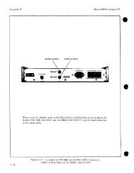
INDICATORS AND CONNECTORS<br />
Figure 1-1 shows all panel controls, indicators and<br />
connectors for the Model <strong>1250A</strong>. Specific information is provided<br />
in the following tables.<br />
Table. 1-3: Model <strong>1250A</strong> Front Panel<br />
REFERENCE DESCRIPTION FUNCTION<br />
MI<br />
. .<br />
Circuit test meter Displays relative operation of<br />
circuit selected by circuit<br />
test switch.<br />
S5 Circuit test Selects battery voltage,<br />
switch regulated voltage, oven<br />
current, 5 MHz amp drive, 1 MHz<br />
amp drive, 100 kHz amp drive on<br />
a relative scale.
CONTROLS, INDICATORS AND CONNECTORS (continued)<br />
-- REFERNCE - DESCRIPTION FUNCTION<br />
R3 Fine frequency A 5000 division dial which<br />
adjustment reads frequency in parts X 10<br />
to the -10th the range is<br />
approximately 000.0 X 10 to<br />
the -10th to 999.9 X 10 to<br />
the -10th.<br />
Coarse frequency Removal of the seal screw<br />
adjustment allows access to the adjustment<br />
capacitor which has a total<br />
range of 2 300 X 10 to the<br />
-9th. (Use AUSTRON tool number<br />
02096061.)<br />
BATT<br />
CHARGE<br />
STBY RESET<br />
LINE<br />
(BNC) 5 MHz<br />
(BNC) 1 MHz<br />
(BNC) 100 RHZ<br />
In the down position the<br />
internal batteries are on<br />
trickle charge and in the up<br />
position on high charge.<br />
Is lighted when the internal<br />
batteries are on high charge.<br />
Momentary switch that disables<br />
STBY after ac power is applied.<br />
The RESET position may be up<br />
or down but the switch moves<br />
only to the RESET position<br />
and returns to NORMAL when<br />
released.<br />
Indicates that the primary ac<br />
has failed at some time.<br />
Indicates the presence of<br />
primary ac.<br />
5 MHz output port.<br />
1 MHz output port.<br />
100 kHz output port
CONTROLS, INDICATORS AND CONNECTORS (continued)<br />
Table. 1-4: Model <strong>1250A</strong> Rear Panel.<br />
REFERENCE DESCRIPTION FUNCTION<br />
J6 (BNC) 5E 5 MHz output port.<br />
57 (BNC) 1 MHz 1 MHz output port.<br />
58 (BNC) 100 KHz 100 kHz output port.<br />
J9 (BNC) CLOCK A 1 MHz sine at 2 0.5 Vrms<br />
OUTPUT into 1 kilohm.<br />
J10 (BNC) TUNING<br />
8<br />
Input port that accepts<br />
VOLTAGE dc voltage in range of<br />
- + 5 Vdc to adjust the<br />
frequency a total of 2 5<br />
X 10 to the -8th.<br />
XF2 BATT<br />
52 EXT POWER<br />
ALARM<br />
115/230<br />
POWER<br />
1 A Slo-Blo fuse which<br />
protects the battery pack.<br />
1 A Slo-Blo fuse which<br />
protects the power transformer.<br />
1 A standard fuse which<br />
protects the voltage regulator.<br />
3PDT switch connects ac,<br />
external dc and internal<br />
batteries to the standard.<br />
MS connector accepts 17 Vdc,<br />
to 35 Vdc pin A negative<br />
ground and pin B positive dc<br />
input, pins C and D provide<br />
contact closure (5 A, 120 Vac<br />
rating) when primary ac fails.<br />
Select 115 Vac or 230 Vac<br />
operation.<br />
Input port for primary ac.
2. INSTALLATION<br />
2.1. SCOPE OF SECTION<br />
Section Two describes the steps required to prepare the<br />
Model <strong>1250A</strong> <strong>Crystal</strong> Frequency Standard for operation and<br />
reshipment to another location. Included in this section are<br />
instructions for unpacking, inspection, installing and storing<br />
the unit, along with lists of fundamental electrical requirements<br />
and accessories.<br />
2.2. UNPACKING AND INSPECTION<br />
2.2.1. Initial Inspection<br />
Immediately report any equipment damage to the carrier<br />
making delivery and to AUSTRON, Inc. Inspect internal components<br />
and circuits by removing the dust covers. Examine exterior and<br />
interior parts carefully.<br />
2.2.2. Circuit Boards<br />
Exercise care when removing or installing circuit<br />
boards. The recommended installation procedure is to align the<br />
board contacts with the connector, then carefully insert the<br />
board as far as it will go.<br />
<strong>1250A</strong>.<br />
NOTE<br />
Component side to the right when facing the<br />
front panel.<br />
CAUTION<br />
Turn power off before removing or installing<br />
boards.<br />
2.3. OPERATIONAL INSTALLATION<br />
The following accessories are received with the Model<br />
1. One three conductor power cord for 115 Vac<br />
operation.<br />
2. One mating dc and ALARM connector.<br />
3. One cable clamp for MS type connector.<br />
4. Two sets of spare fuses.<br />
5. Two technical manuals.<br />
6. One PCB extender board.<br />
7. One tuning wand.
OPERATIONAL INSTALLATION (continued)<br />
2.3.1. Power Connections<br />
This unit operates on 115 Vac or 230 Vac 210 percent, 48<br />
Hz to 440 Hz. Before connecting the power cable to the source,<br />
verify switch lAlSl is in the correct (115 or 230) position and<br />
that lAlFl is 1 amp Slo-Blo 3 AG for 115 Vac or 0.5 amp Slo-Blo<br />
for 230 Vac.<br />
2.3.2. Cable Connections<br />
With the MS type connector sudilied, fabricate a cable<br />
to supply the dc standby power. The connectors as as follows:<br />
A<br />
SUPPLY B<br />
C<br />
ALARM D<br />
- Pin ---- Connection<br />
2.3.3. Installation<br />
GND<br />
17 Vdc to 35 Vdc<br />
Contact closure<br />
Rated at 5 A 120 Vac<br />
The Model <strong>1250A</strong> is rack-mounted in a standard 19-in rack<br />
or bench-mounted on a stable surface, as required. Choose a<br />
location away from components producing high temperatures.<br />
2.4. PREPARATION FOR RESHIPMENT<br />
Turn power off. Check to see that mounted components<br />
are in place and secure.<br />
CAUTION<br />
If shipment or storage duration of greater<br />
than 30 days or storage temperatures greater<br />
than -40°C to 50'C is anticipated, the Nicad<br />
batteries should be removed by a qualified<br />
technician.<br />
For shipping, enclose the unit in a suitable water-and-<br />
vapor-proof plastic bag. Heat seal or tape the plastic bag to<br />
ensure a moisture-proof closure. When sealing the bag, keep<br />
trapped air volume to a minimum.<br />
Ensure shipping container is a rigid box of sufficient<br />
size and strength to protect the equipment from damage. The<br />
original shipping container and packing material may be reused if<br />
it is still in good condition.
a<br />
3. OPERATING INSTRUCTIONS<br />
3.1. SCOPE OF SECTION<br />
Section Three provides instructions for operating the<br />
Model <strong>1250A</strong> <strong>Crystal</strong> ~ re~ienc~ Standard. Included -are general<br />
descriptions for operation. Please read the following paragraphs<br />
before operating the unit.<br />
3.2. NORMAL OPERATION<br />
,<br />
After installing the unit, place the power switch level,<br />
S2, in the ON position (up).<br />
Check the circuit test monitor and verify the following:<br />
1. BATT between 40 and 60.<br />
2. REG between 40 and 60.<br />
3. OVEN less than 10 (oven cold).<br />
4. 5 MHz between 40 and 60.<br />
5. 1 MHz between 40 and 60.<br />
6. 100 kHz between 40 and 60.<br />
Check the battery charge switch, 53, by placing the<br />
lever in the up position. Note the CHARGE indicator, DS2, lights<br />
and battery-voltage indicator moves up scale slightly. Place the<br />
battery charge switch in the down position.<br />
Disconnect the ac power cord, W1. Note the standby<br />
indicator, DS3, is on and pins C and D on the external power and<br />
ALARM indicator, 52, read zero ohms. Reconnect the ac power cord<br />
and note that C and D are now open.<br />
The line indicator, DS1, is on. Place the standby reset<br />
switch, S4, in the RESET - position and release; note the STBY<br />
indicator is dark.<br />
Check the battery power-up circuit in the following<br />
manner, when the unit under test (UUT) has charged or partially<br />
charged internal battery pack. Remove the ac power and the<br />
external dc power. Place the power in the OFF position (down).<br />
Place the power switch in the ON position (up). Set the circuit<br />
te5.t switch, 55, to the REG position. Place the standby reset<br />
switch, S4, in the RESET position and release. The regulated<br />
voltage is present on the meter, MI. Reconnect the ac and dc<br />
power.<br />
Verify the output at the 5 MHz, 1 MHz and 100 kHz ports<br />
are present and at least 1 Vrms into 50 ohms load. Also, check<br />
the clock output for 1 MHz 0.5 Vrms into a 1 kilohm load.<br />
-
NORMAL OPERATION (continued)<br />
At this time, allow six hours for the Model <strong>1250A</strong> to<br />
stabilize.<br />
CAUTION<br />
Do not make any frequency adjustments during<br />
this time.<br />
Check the circuit test monitor in the OVEN position and<br />
verify it reads between 40 and 60. ,pecord the values of all<br />
monitor positions at this time and save as an indicator of proper<br />
operation for future reference.<br />
After stabilization, the frequency may be corrected with<br />
the fine frequency control, R3, by comparing the output to a<br />
reference source with a phase comparator (AUSTRON Model 1201A) or<br />
a frequency meter. Refer to Figure 3-1.<br />
When corrections can no longer be made with the FINE<br />
frequency control, return the control to 750 on the dial and<br />
remove the COARSE tuning access screw. With the tool provided<br />
(02096081), engage the tuning capacitor and set the oscillator on<br />
frequency. Allow fifteen minutes for the oven to stabilize.<br />
Make the final frequency correction with the fine frequency<br />
control.<br />
External frequency adjustment is made in the following<br />
manner. Set the FINE frequency control on the front panel to 750<br />
when using 25 Vdc applied to the TUNING VOLTAGE input port,<br />
J10, on the rear panel.<br />
Other input voltages up to 20 V may be used as long as<br />
the algebraic sum of the input voltage and the fine tuning dial<br />
reading, read in volts (0.00 V to 9.99 V), is greater than zero.<br />
Because of the non-linearity of various voltage/dial<br />
combinations, it is advisable to calculate frequency versus<br />
voltage curves to determine the gain constant for various servo<br />
loop applications.<br />
Batteries should be charged for sixteen hours after they<br />
have been depleted to the point that the cut-out circuit on A2<br />
has disconnected them.
Figure 3-1: Phase Comparison.<br />
3-3
4. FUNCTIONAL DESCRIPTION<br />
4.1. SCOPE OF SECTION<br />
Section Four details the theory of operation of the<br />
Model <strong>1250A</strong> <strong>Crystal</strong> Frequency Standard. Included are block<br />
diagrams, schematics, detailed circuit descriptions and assembly<br />
drawings.<br />
4.2. CIRCUIT ANALYSIS<br />
The following circuit descriptions detail the functions<br />
and purposes used in operating the Model <strong>1250A</strong>.<br />
4.2.1. Power Supply<br />
The Model <strong>1250A</strong> power supply is designed to perform<br />
several functions, such as automatic battery switchover,<br />
automatic external dc switchover, automatic low voltage battery<br />
cut-out, ac interruption indication and electrical tuning.<br />
Diode CR1 is used as an external dc switch, when back<br />
biased by the bridge input the external dc is cut off. The<br />
transistor Q1 is used as a series regulator to supply the load.<br />
The reference voltage for €21 is supplied by the batteries through<br />
relay K1, which is held closed by Q2 whose bias is furnished by<br />
CR3 which along with resistors R1, R2 and R3 detect the battery<br />
voltag;.<br />
The gate of the SCR CR3 is fired by the ac cut-out<br />
relay; this lights the standby lamp until the reset is pressed.<br />
Components C2, R7, R8 and R9 form a linearizing circuit<br />
for the oscillator varicap.<br />
Resistors R10 and R11 are used for voltage monitoring.
4.2.2. AUSTRON Model 1150 <strong>Oscillator</strong><br />
The AUSTRON Model 1150 <strong>Oscillator</strong> employs a high-<br />
quality, high temperature bake-out crystal unit which, together<br />
with special oscillator circuitry, is mounted in a proportional<br />
oven. A high-stability feedback amplifier is used in connection<br />
with an automatic gain control (AGC) system to maintain the<br />
crystal drive power at the low constant value that is necessary<br />
to attain high frequency stability.<br />
The Model 1150 <strong>Oscillator</strong> is a sealed unit and as such<br />
is not field repairable. Any attempt to open this unit voids the<br />
warranty. Send to the factory for repaif or replacement.<br />
4.2.3. Sine Converter<br />
The sine converter PCB contains a 5 MHz clipper, 5 MHz<br />
buffer gate, a divide-by-five stage, a decade divider and two<br />
sine converter buffer amplifiers.<br />
The 5 MHz sine wave from the internal oscillator is<br />
supplied through isolating resistor R2 and coupling capacitor C1<br />
to the input of a two-stage direct coupled amplifier made up of<br />
61 and Q2. The output of this amplifier is a 5 MHz pulse which<br />
has the proper characteristics to drive (UlB), (UIC), (UlD) which<br />
comprise a 5 MHz buffer gate. The output of (UlC) is a 5 MHz<br />
TTL signal which is supplied to (U2).<br />
IC (U2) is a divide-by-five stage which produces a 1 MHz<br />
TTL output from the 5 MHz TTL input. The 1 MHz TTL output from<br />
(U2) is fed through a low pass filter R9, C6, to the base of a<br />
collector tuned RF amplifier. The resulting 1 MHz sine wave at<br />
the secondary of TI is used to drive the 1 MHz output buffer.<br />
IC (U3) is a decade divider which produces a 100 kHz TTL<br />
output from a 1 MHz TTL input supplied from (U2). The 100 kHz<br />
TTL signal is fed through a low pass filter R8 and C5 to the base<br />
of 64, a collector-tuned output amplifier. The 100 kHz signal<br />
present at the secondary of T2 is used to drive the 100 kHz<br />
output buffer.
4.2.4. Output Amplifiers<br />
The output amplifier PCB contains three similar<br />
amplifiers which operate in a like manner. For example, we will<br />
discuss the 5 Mhz amplifier.<br />
Components R1, CR1 and C1 form a monitoring circuit to<br />
check the input to the amplifier. <strong>Crystal</strong> Y1 in an input filter<br />
with R2 as its load. The transistors Q1 and Q2 form a two-stage<br />
common emitter, collector-tuned amplifier with negative feedback.<br />
The feedback ratio is determined by R7 and R6. These amplifiers<br />
have been designed to allow a minimum level change for a maximum<br />
load change.
2. f f SELECT FOR MID- SCALE ON MI.<br />
1. SELECT FMI OUTPUT LEVEL IV RMS WTO 30 OHMS.<br />
NOTES:<br />
TOLERANCES<br />
VNLIII OIKm-IS< I.fElFllD<br />
SCHEMATIC DIAGRAM -<br />
OUTPUT AMPLIFIER
4 3 + L I A<br />
.DENOTES SELLCTE1 VALUE<br />
/<br />
FIG 4-6<br />
MOUNT DbJ ClRLU\? SIDE<br />
FEPRITE SAD FEKQITE EEAD<br />
254 97337 i<br />
NEXT ASSY<br />
APPLICATION<br />
QTY<br />
REQD<br />
-I<br />
NOTE '.<br />
WHEN INSTALLING 7-3, COMUECT<br />
PRIMARY FINISH LEAD W\THOUT<br />
TR\MM\rJG EXCESS LEWTW.<br />
ITEM REF DES<br />
NO<br />
UNLESS OTHERWISE SPECIFIED<br />
DIMENSIONS ARE IN INCHES<br />
W NOT SCALi DRAWlNt<br />
--<br />
TOLERANCES<br />
UNltSS OIHtRWl5r SPlCll1t0<br />
I250 a<br />
USED ON<br />
DEC<br />
rucT<br />
ANG<br />
ZON~LTR' DESCRIPTION<br />
- RELEA~ED<br />
A<br />
g<br />
G<br />
E<br />
F<br />
6<br />
H<br />
PART NO<br />
ENGINEER ,&. \I, ~(v',~cX<br />
cnicKro IR& 13-~.'76.<br />
DRAFlSMAH /-~~€~13.17.?6<br />
LIST OF MATERIAL<br />
REVISIONS<br />
DATE A:<br />
3-2s-X M<br />
PEVI~E~ Pdcrocc <strong>To</strong> Aa;,~r L-JI/,IH ~ L P L ~ c- U<br />
PX =O 1432<br />
5-12-7&<br />
EL0 15.10 : Clo WAS 410; AGDED 15on<br />
RE5 A L R ~ ~ y2 S<br />
EC3 ZZIO: IDENTIFIED WINDINGS ON TI,<br />
2.,3 73<br />
T2,6 T3; ADDEDVALUCSTOYI BY2<br />
,-<br />
Fz'j's~~ CAR-: LIZ1 :'f~ C_W. zsLT 4.1577 .<br />
2EV ISES PARTS UST R YCEErJ LCD Z m 12.11- 7:' ,-<br />
hGDED N3TE FOR TZ FL> ELo. j430 ,-<br />
C.zcF.Q<br />
PIL REVISEb PER ECD 7901 ?WI~ 10.P25'5<br />
P/L CIIRNC-E ONLY o;*- EC04343 2.5--6:,<br />
NOMENCLATURE<br />
AUSTRON A.<br />
7:<br />
P BOARD A5s~-<br />
(~UTPUT AMPLIFIER<br />
SIZE<br />
2<br />
COC T<br />
NO:!-^: - 2<br />
-<br />
103 96986<br />
SCALE I:\ 1 SHEET 1<br />
(<br />
,
4.2.5. Chassis Functions<br />
The Model <strong>1250A</strong> chassis performs several functions, such<br />
as: battery pack mounting, high and low charge, unregulated dc,<br />
supply, and oscillator decoupling.<br />
The internal Nicad battery pack is mounted to the inside<br />
rear support member. These batteries have a four ampere-hour<br />
capacity which powers the Model <strong>1250A</strong> for ten hours at 25*C. The<br />
batteries are the reference for the voltage regulator, A2.<br />
WARNING<br />
Do not operate unit with 'the batteries<br />
removed.<br />
WARNING<br />
Do not short Nicad batteries; high currents<br />
are available which will damage tools, wiring<br />
and batteries.<br />
The low charge current for the batteries is through<br />
R1 and the high charge current through R1 and R2 connected in<br />
parallel by switch S3B.<br />
The unregulated dc supply is composed of TI, C1, and<br />
bridge Al. The input is selected by S1 for 115 Vac or 230 Vac.<br />
Choke L1 and capacitor C1 form a decoupling network of<br />
the Model 1150 <strong>Oscillator</strong>.<br />
The relay K1 performs the alarm function; when the<br />
primary ac fails, it also fires the standby lamp circuit located<br />
on A2.<br />
4.2.6. Output Filters<br />
The two output filters have three LC filters which are<br />
tuned at 5 MHz, 1 MHz and 100 kHz. These filters are mounted on<br />
the output BNC connectors on both the front and rear panels.
4<br />
-4<br />
3<br />
r I REVISIONS 1<br />
APPLICATION<br />
2<br />
ZONE 1 LTR I DESCRIPTIOH DATE ( APPD<br />
- 1 ca .:.,-?L, Il lq.;,: 1 , *.r.-<br />
."SI,W If..<<br />
BOTTOM VIEW<br />
MODEL 1250 A<br />
1
NOTES :<br />
1. (/Sf 22 AWG WIRf<br />
BLACK
- 1<br />
STANDARD
5. MAINTENANCE<br />
5.1. SCOPE OF SECTION<br />
Section Five provides the technician with the general<br />
approach to maintaining the Model <strong>1250A</strong> <strong>Crystal</strong> Frequency<br />
Standard. Included are trouble analysis guides and general<br />
maintenance procedures. Please review Section Four, Functional<br />
Description, for detailed information.<br />
TROUBLE ANALYSIS GUIDE<br />
The following troubleshooting table provides specific<br />
information on symptoms and probable causes.<br />
Table. 5-1: Troubleshooting Table.<br />
Symptom<br />
LINE indicator<br />
DS1 is dark.<br />
Probable Cause<br />
1. AC power not available.<br />
2. Power switch not on.<br />
3. Power cord not connected.<br />
4. 230 Vac selected when on<br />
115 Vac.<br />
5. Indicator burned out.<br />
2. CHARGE indicator 1. Indicator burned out.<br />
fails when LINE 2. Switch S3 open.<br />
is lighted.<br />
STBY is dark. 1. Indicator burned out<br />
2. SCR circuit on A2.<br />
3. Relay K1 bad.<br />
4. Battery circuit 1. Blown F2.<br />
test reads high. 2. Open S2.<br />
3. Battery pack open<br />
5. Reg. circuit test 1. Check battery circuit test.<br />
reads high. 2. 61 on A2 shorted.<br />
3. K1 on A2 not closed.<br />
6. Oven circuit test 1. A3 is in warmup stage.<br />
reads low. 2. Supply voltage to A3 low.<br />
3. Defective A3.<br />
7. 5 MHz circuit<br />
test reads low.<br />
1. Check output of A3 with A4<br />
and A5 removed; should be<br />
1 vrms.<br />
2. Check A5 meter circuit.
Troubleshooting Table (continued)<br />
Symptom ---- Probable -- Cause<br />
8. 1 MHz circuit test 1. Check output of A4 with A5<br />
reads low. removed; should be 1 Vrms.<br />
2. Check A5 meter circuit.<br />
9. 100 kHz circuit<br />
test reads low.<br />
1. Check output of A4 with A5<br />
removed; should be 1 Vrms.<br />
2. Check A5 meter circuit.<br />
10. 5 MHz output not 1. Check output of A5.<br />
present. Circuit 2. CheckSA6 or A7.<br />
test meter reads OK.<br />
11. 1 MHz output not 1. Check output of A5.<br />
present. Circuit 2. Check A6 or A7.<br />
test meter reads OK.<br />
12. 100 kHz output not 1. Check output of A5.<br />
present. Circuit 2. Check A6 or A7.<br />
test meter reads OK.<br />
13. Clock output not 1. Check A4.<br />
present.<br />
14. Tuning voltage input 1. Check A2.<br />
has no effect. 2. Defective A3<br />
15. A3 has no output. 1. Check supply A2.<br />
2. Remove A4 and A5; if still not<br />
present, A3 is defective.<br />
16. Cannot adjust coarse 1. Tuning tool broken.<br />
frequency. 2. Defective A3.<br />
17. Batteries will not 1. Not charged for 1 6 hours.<br />
operate unit for 2. High charging circuit not<br />
10 hours. delivering 3 00 to 5 00 rnA.<br />
3. Replace batteries.<br />
5.3. GENERAL MAINTENANCE<br />
..<br />
Check capacity of Nicad batteries every six months.<br />
Deep discharge and recharge for sixteen hours. When batteries do<br />
not give required standby capacity, replace them.<br />
No other periodic maintenance is required.
6. PARTS LIST<br />
6.1. SCOPE OF SECTION<br />
Section Seven provides the list of replaceable parts<br />
which include the reference designator, the part description, and<br />
the part number. For convenience in ordering from local<br />
suppliers, the manufacturer's part number and the manufacturer's<br />
Federal Identification Code (FIC) are also given where<br />
applicable.<br />
6.2. ORDERING REPLACEMENT PARTS<br />
<strong>To</strong> order replacement parts from AUSTRON, Inc., address<br />
the order to:<br />
AUSTRON, Inc.<br />
P. 0. Box 14766<br />
Exit 248, N. IH 35<br />
Austin, Texas 78761<br />
Specify for each part, the AUSTRON part number, revision<br />
letter, part description, circuit reference designator and the<br />
printed circuit board on which the part is located. <strong>To</strong> order<br />
parts not listed in this section, give a complete description of<br />
the function of the part and its location in the unit.<br />
Manufacturer part numbers as shown will change<br />
occasionally as vendor items are re-evaluated or as improved<br />
components become available. The equivalent part currently used<br />
in production at the time orders are received will be shipped.<br />
Where the manufacturer's part number or FIC is missing, any<br />
reputable manufacturer's part of the appropriate value, indicated<br />
in the description, may be used.<br />
6.3. MODEL PARTS<br />
Refer to the parts list for AUSTRON part numbers for the<br />
Model <strong>1250A</strong> <strong>Crystal</strong> Frequency Standard. All screws are standard<br />
hardware items.
MANUIL PARTS 11 ST VODEL 1?50A<br />
ASSFF'RLY ~ W F Q s7n 5, ~ F . ~ H L ; ~ Owit1 O ~ H L<br />
AsSEr4Hl.Y NCIqHEP 3b497306<br />
C\Ff EkEtlCE LIESIGNATIIP PHFFlx<br />
QUANTITY 1 FA<br />
C.FF DES PART PESCRIPTION<br />
1 t1i 1 l IlG TOOL<br />
PCB ASSY, EXTFl.IT)tR<br />
UPtRAT ([IN & MbINTFNAPlCt KANUAL<br />
F-IIJAL ASSY FWFO STD<br />
CLdtfP I 4N3057-6<br />
Cnr~Nc STRAIGHT 4 SUCKFT CONTACl<br />
FUSE 3AG 1 APP 25OV<br />
F ~ S E 3 ~ 6 I AlnP ?50V<br />
FUSF 3A6 1 AMP ?50V<br />
FUSE 3AG 1 AMI' 25OV<br />
FUSF 36G 1 AMP 25nV<br />
FUSE 3AG 1 AMP 250V SLU BLD<br />
FIJSE 3AG 1 bvP ?50V SCO BLO<br />
r USE ~ A G 1 AWF 75nv SLU LO<br />
FUSF JAG 1 AMP 750V SLO BLU<br />
FIJSF 3@G 1 APP 250V SLO HLU<br />
HFG PART FIC
W' -.'ezV- -<br />
>.- . .<br />
' - .-<br />
KANU4L PARTS LIST HODFL 1?!50A 15nc~n6<br />
ASSEbHLY FIVAL AfSY FHFO STU<br />
ASSFP*HCY NVtqI!FR 25497301<br />
HEF~HFNCE UESIGNATOP PFEFIX 1<br />
OUAYT ITY 1 FA<br />
kEF DES PART DkSCRIPTIUN<br />
CHbSSIS CkT ASSY SrlMHZrlflOKHZ U/E<br />
DCH ASSYc DIOPE HPIDGE<br />
PCB ASSv, FflIFW SOPPLY<br />
SPEC XTAL OSC 1150 (In-RSDFG)<br />
PCB AfSY SINE CnNVLRTFR<br />
YCH ASSVr IIlJTPUT at\PLIFIEP<br />
PC R0fiP.T: ASSY-UUTPL'T FILTFH(AAtb7)<br />
PC RUAWn ASSY-UIJTPUT FIlTFR(AhGA7)<br />
HFG PAKT
U U l . U b k J ~ U d ~ A J b k J & U J >>>a = m C<br />
UUvUVUU~vUUUu C C Y C +<br />
1 1 1 1 1 1 1 1 1 1 1 1 - som s s z<br />
aC.GCCOCCGCCC+ clrr ++ A -I 0<br />
r u m<br />
mmm<br />
1 1 1<br />
3'0'0<br />
FPF<br />
UUU<br />
Y Y r
Lo<br />
LL'<br />
3<br />
c c u - I cd J-'<br />
H 4 \ 0 Z z3 0c<br />
*ZZ+% c urn rnrn<br />
C C GOC a m ~22 32<br />
u99 mz c3<br />
C QXX C U q I-P r2
ASSEEiqLY PC9 ASSYT DlOnE URInGF<br />
ASSEHRLY NUMHER 10395977<br />
REFERENCE LESIGNATUP PREI JX 141A1<br />
c?llaNTITY I €A<br />
REF DES PAPT DESCPIPT ION AllSTCrflN PART MFG PERT<br />
CH1 60UPRV 1 A I'IU 5 PFCT DU-41 7011~4005 1116005<br />
CQ2 600PKV 1A Dl0 5 KCCT Orl-41 7nllN4005 11J6Or?5<br />
Ccl.3 6OIIPEV 1A ()Ill S RECT Otl-41 7Ullb!4005 IN4005<br />
CQ4 6CdPPV 1A DrU S HECT nu-41 70111940q5 I NbOn5<br />
FIC
cU<br />
a<br />
rC\<br />
f-<br />
0<br />
0<br />
u x<br />
C IF<br />
4r-N<br />
I z c<br />
*-3<br />
ncu<br />
om2<br />
nnr(<br />
u m<br />
c l-<br />
4*N<br />
GC c<br />
I I C+<br />
cru<br />
n-tz<br />
CCC<br />
as4<br />
C C C<br />
3 3 r-<br />
- %'<br />
C<br />
4 *<br />
I<br />
> 3<br />
W C<br />
rr, +<br />
V<br />
u CU<br />
3 a<br />
u<br />
3 cn<br />
H f-<br />
0 0 3<br />
I u -<br />
rn s<br />
c 2<br />
Y X<br />
r( a<br />
3<br />
rt<br />
w +<br />
W z<br />
cn a<br />
I- <<br />
A 4<br />
b d<br />
W C ><br />
dmz<br />
0<br />
Zno<br />
xu0<br />
3v-l<br />
4<br />
-(La<br />
OOU<br />
- - - -<br />
rc LLr - -FFz<br />
w e mZb-+rr)~6r3 2353<br />
LI! cuU,I-- X xxxx
YAtJIJAL PARTS LIST MnOFL 125OA<br />
ASSEptlLY SPEC XT4L OtC 1\50 (70-A5DEC)<br />
ASSLYPLY NU'"IBEP. 30295Q3P<br />
HEFEPFtJCF OESIGNATUR PPf FTX l A l A 3<br />
QIIAhTITY 1 €A '<br />
REF DES PART OESCRIPTIUN AtJSTHOIJ PhHT tlFG PART<br />
THIS IJtJIT IS SEALEL AND AS SUCH IS<br />
IJVT F ltl-D KFPAIP 4QLF. RFTIJHN TO<br />
FACTUQY FOR KFPAIR nk QEPLACtNENT.
T73U<br />
OOCU<br />
Z Q V V ,<br />
r/)*v)o
MAFJtjAL PARTS LIST FWVFL 1750A<br />
ASSkFnLY PCB ASSYt UllTpUT AtlPLIF IER<br />
ASSkhRLY hlJMrJFR 10396986<br />
HFFERFIK~ UESIGNATOP FRFFIX 14145<br />
~JI~AI~TITY 1 F4<br />
REF DFS PART DESCRIPTIUN AllSTKnN PART<br />
CAP SC~L TAIJT AXL I UF 3sv 10% 60~~17-0ins<br />
CAP UIP tllch 470 PF 500V 05% 603000-n471<br />
CAP SOL TANT ~ X L 1 UF 35V 10% 600017-Ql05<br />
CPY UII' PIJCA 470 PF 50nv 0 5 603~~0-f1471<br />
~<br />
CAP SOL TAIJT AXL 1 UF 3 5 ~ 10% 60~017-~ln5 CAP DID M ~ C A<br />
CAP SOL TANT<br />
47n<br />
PXL 1<br />
PF 50nv 0 5 60~w-0471<br />
~<br />
UF 35v Ink, 608017-nln5<br />
CAP PIP VlC4 3300 PF 509V 05; 603000-0372<br />
1 IIC 3511 1ng bngnl7-~ios<br />
CAP SOL TBNT<br />
CAP I~II~ PICA<br />
~ X L<br />
3300 PF sonv us% ho3000-0332<br />
CAP SnL TAIJT PXL I UF 35V 10% 608017-0105<br />
.01A UF 50V<br />
75 PKV<br />
75 PH\t<br />
10 CAP FlLM<br />
1'10 S SIC;<br />
Ul(' S SIC;<br />
6Q7050-01P3<br />
7011f.(014<br />
7f'111JQl4<br />
I5 DWV Dl0 S SIG 7011 id914<br />
470 1Jti C l-IUK k 751104-0471<br />
2200 Ilti CHUKE 751104-0222<br />
L~OQOUH CH~K E - 1 s 0~-n273 ~<br />
XSTR FPN o.qlr TU-32 ~~ZZIJWM<br />
0.31~ ~n-92 XSTP YNPS SH 7022rJ3906<br />
YSTP. NPY 0.31W<br />
o. 31 w rn-92<br />
TO-92<br />
XSTP PF~PS SH<br />
7n22~3904<br />
7027 1439%<br />
X S ~ R NI"J n.313 TU-02 ~ o z I I J . ~ ~ ~ ~<br />
Ue31M TO-92<br />
SELECTED<br />
X5TR YNPS SH 7c22N79n6<br />
UES FYU C9M"<br />
LES rxb carp<br />
470 nw 1 / 4 ~ 10% 651102-0471<br />
15 t( 1 / 4 ~ 10% 651137-0153<br />
l;FS FXD C@MP 1.5 K 1/4H l 0 X 651102-n152<br />
ClES FXL) COED<br />
llFS )XU CIIMP<br />
SFLECTLf<br />
J.<br />
2 2<br />
K 1/4H 10% h51107-0102<br />
n!w ~ 1/4rl lfrx 651107-n2?1<br />
KES Fxl, Cnl4P 47 PIiM 1/4d 10'4 651107-0470<br />
KFS FXV COPP 68 ntctr I / ~ K 10x G~~Io?-~~Rc)<br />
15 OCT Rb<br />
MFG PART FIC
a<br />
W<br />
C<br />
u (A<br />
c a<br />
2 4<br />
a C<br />
lc d<br />
C<br />
x<br />
- k<br />
Z) u<br />
a 9 U'<br />
tar<br />
3 P 0<br />
3 9<br />
0 a<br />
o h 3<br />
rct<br />
m44<br />
a z<br />
OQ.@@Q'Q Q'Q' Q'QQ‘Q. @@ hlNR199<br />
u uvuuuu 94 uuuu uu r-r-f-CC<br />
cr mmnmmm nn mnnm nn Q ~ Q A A<br />
U r~rr(dr r- nd u4au.t<br />
C D O D ~ C O ~ ~ ~ Q C O Q G ~ G ea. NNN~-+<br />
t<br />
H<br />
6<br />
0 dYhL*Y* LY<br />
Cr.rr.&Nd CC<br />
c=, r-r-mmory ccr-<br />
LL UqHrrh
PANIJAL PARTS LIST MOUFL <strong>1250A</strong> 15 OCf 86<br />
4SSFMHLV PC ROARn ASSV-OUTDUT F ILTFR (A6&4 I )<br />
LSSFt.lRLV NI'YREF. -10397323<br />
REFtHFNCE UESIGtJATflR PREFIX 161A6<br />
QUANTITY 1 €A<br />
REF u€S PART OESCRIPT1W AIISTRON PART MFG PART<br />
C1 CAP DIP HICA 22n0 PF 5 0 1 ~<br />
05% 693n00-0222 DM19-222J<br />
C2 C4P DIP HICb 1000 PF 10VV 053 bn3nOn-0102 CDlSFA107JP3<br />
C3 a018 UF SOV 10 C6P FILM 607050-OlR3 71QDlARlR3K50OAX<br />
L I 5rHZ FILTER INDllCTUQ 4.6UH 75197469<br />
C2 lYHL FILTER INUUCTOR 75UH 15197468<br />
L3 INUIJCTUKr100KHZ F ILTtW 75197467
INDEX<br />
A<br />
AUSTRON Model 1150 <strong>Oscillator</strong>, 4-7<br />
C<br />
Cable Connections, 2-2<br />
Chassis Functions, 4-19<br />
CIRCUIT ANALYSIS, 4-1<br />
Circuit Boards, 2-1<br />
CONTROLS, INDICATORS AND CONNECTORS, 1-12<br />
D<br />
DESCRIPTION OF CHANGES FOR SPECIAL OPTIONS, 1-2<br />
Dwg. No. 10394595-* Rev GI 1-9<br />
Dwg. No. 10395533 Rev L, 4-5<br />
Dwg. No. 10396025-* Revs, 4-11<br />
Dwg. No. 10396986 Rev HI 4-17<br />
Dwg. No. 12394695 Rev A, 1-7<br />
Dwg. No. 12396096 Rev Dl 4-9<br />
DWg. No. 12396100 Rev F, 4-3<br />
Dwg. No. 12397320 Rev A, 4-15<br />
Dwg. No. 12397328 Rev A, 4-23<br />
Dug. No. 12398452 Rev -, 1-5<br />
Dwg. No. 12497325 Rev -, 4-20<br />
Dug. No. 12497326 Rev -, 4-21<br />
Dwg. No. 12497327 Rev -, 1-15<br />
Dwg. No. 20197336 Rev A, 4-25<br />
Dwg. No. 25497307-* Rev C, 4-27<br />
F<br />
FUNCTIONAL DESCRIPTION, 4-1<br />
G<br />
GENERAL DESCRIPTION, 1-1<br />
GENERAL MAINTENANCE, 5-2<br />
I<br />
Initial Inspection, 2-1<br />
INSTALLATION, 2-1, 2-2<br />
M<br />
MAINTENANCE, 5-1<br />
MODEL PARTS, 6-1<br />
MODEL VARIATIONS, 1-1<br />
N<br />
NORMAL OPERATION, 3-1<br />
0<br />
OPERATING INSTRUCTIONS, 3-1<br />
OPERATIONAL INSTALLATION, 2-1<br />
ORDERING REPLACEMENT PARTS, 6-1<br />
Output Amplifiers, 4-13<br />
Output Filters, 4-19<br />
P<br />
P/L No. 10395533, 6-7<br />
P/L No. 10395977, 6-6<br />
P/L No. 10396025, 6-9, 6-10<br />
P/L No. 10396986, 6-11, 6-12<br />
P/L No. 10397323, 6-13<br />
P/L No. 20497308, 6-4, 6-5<br />
P/L No. 25497307, 6-3<br />
P/L No. 30295838, 6-8<br />
P/L No. 30497306, 6-2<br />
PARTS LIST, 6-1<br />
Power Co~ections, 2-2<br />
Power Supply, 4-1<br />
' PREPARATION FOR RESHIPMENT, 2-2<br />
PURPOSE OF EQUIPMENT, 1-1<br />
S<br />
SCOPE OF SECTION, 1-1, 2-1, 3-1, 4-1, 5-1, 6-1<br />
Sine Converter, 4-7<br />
SPECIFICATIONS OF EQUIPMENT, 1-11<br />
T<br />
TROUBLE ANALYSIS GUIDE, 5-1<br />
U<br />
UNPACKING AND INSPECTION, 2-1