Metallized Particle Interconnect
Metallized Particle Interconnect
Metallized Particle Interconnect

You also want an ePaper? Increase the reach of your titles
YUMPU automatically turns print PDFs into web optimized ePapers that Google loves.
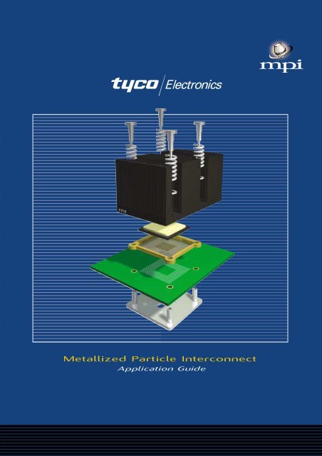
<strong>Metallized</strong> <strong>Particle</strong> <strong>Interconnect</strong><br />
Application Guide
MPI<br />
Columns<br />
2<br />
What is MPI?<br />
The MPI contact system allows the user a means of parallel<br />
interconnection through the use of compression activated<br />
contacts. MPI is a high temperature, flexible, conductive<br />
polymeric interconnect solution which incorporates piercing<br />
and indenting particles to facilitate penetration of oxides on<br />
mating surfaces. MPI has been designed to meet the board<br />
connection requirements of microprocessors, ASIC’s and<br />
MCM’s used in high-end servers, mainframes, workstations,<br />
storage, telecom and data equipment, desktop PC’s, mobile<br />
PC applications. Other applications include mezzanine<br />
Daughter Card-to-Motherboard, Daughter Card-to-Backplane,<br />
Flex-to-Flex and Flex-to-Rigid interconnects.<br />
How does MPI work?<br />
The MPI conductive column is<br />
molded into an insulator which<br />
aligns the columns over the<br />
desired I/O field that is to be<br />
interconnected. As the two surfaces<br />
are compressed, the metallized<br />
particles encapsulated within<br />
the columns link together, thus<br />
providing the conductive path.<br />
Daughter Card/LGA/Flex<br />
MCM/ASIC<br />
PCB/Backplane<br />
Polyimide<br />
Insulator<br />
LGA Design<br />
Guidelines<br />
Why Choose LGA Packaging?<br />
• Socketing of Microprocessor Model<br />
– Maximum Flexibility of Motherboard Inventory to Meet<br />
Market Demands<br />
– “Make-to-Order” Model Achievable<br />
• Motherboard Build Cycle<br />
– Quick Diagnosis (FCT, ICT)<br />
– Inexpensive Replace and Repair: Now Possible<br />
– Highest process yield<br />
• Package Cost<br />
– Smaller Package (High Density)<br />
– No Ball or Pin Attach<br />
– Flexible design -> short time to market<br />
• Tariffs<br />
– Moving Motherboards with Lower Tariff Restrictions:<br />
Now an Option<br />
• Very Low Profile<br />
– Less than 1 mm<br />
• High Speed<br />
– Short Signal Path Permits 12 GHz or Greater Processing<br />
• Power<br />
Speeds<br />
– Short Signal Path Minimizes<br />
Voltage Drop from Package<br />
to Motherboard<br />
– Compensation of thermal mismatch<br />
Package Considerations<br />
Tyco MPI LGA sockets are design to work with both<br />
Ceramic (CLGA) and Organic (OLGA) microprocessor and<br />
ASIC packages.<br />
Package Design<br />
Design should follow standard industry practices as defined<br />
by JEDEC standards, unless otherwise specified.
Package Pad Pitch<br />
1,00 [.039] or 1,27 [.050]<br />
Notify Tyco if different pitch is required, even < 1,0 mm.<br />
Package Pad Dia<br />
Pitch mm [in]<br />
1,00 [.039]<br />
1,27 [.050]<br />
Package Pad Positioning<br />
Package Flatness<br />
0,08 [.003] across package<br />
Effective Pad Dia. mm [in]<br />
±0,05 [.002]<br />
0,70 [.028]<br />
0,86 [.034]<br />
Pitch Pad to Pad Pad Array<br />
mm [in] T.P. @ MMC T.P. @ MMC<br />
1,00 [.039] Ø 0,10 [.004] Ø 0,25 [.010]<br />
1,27 [.050] Ø 0,15 [.006] Ø 0,25 [.010]<br />
Package Sizing versus Array Size<br />
Center Line of last Pad to edge of package 2,00 mm [.079]<br />
recommended. Notify Tyco Electronics/MPI if less.<br />
Package Pad Plating<br />
Gold Flash 0,25µm [10µ inches] over Nickel 3,8µm [150µ inches].<br />
Gold can be either Hard or Soft as defined by Mil-G-45204.<br />
Either Electrolytic or Immersion plating process can be used.<br />
PCB Design<br />
Guidelines<br />
Board Design Considerations<br />
MPI columns are designed to work with all industry standard<br />
board designs and materials (FR-4, Polyimide, etc.)<br />
Carefull consideration with respect to the layout of the board<br />
should be taken, as most MPI applications will require at least<br />
4 thru-holes for compression hard-ware and 2 thru-(or blind)<br />
holes for alignment pins.<br />
Board Design<br />
Design should follow standard industry practices as defined<br />
by IPC Specification 2221, unless otherwise specified.<br />
Board Pad Pitch<br />
1,00 [.039] or 1,27 [.050]<br />
Board Pad Dia<br />
(InPad Via Design)<br />
Pitch Pad Dia. ‘A’ Max Via Dia.<br />
mm [in] ± 0,03 [.001] ‘B’ (After Pltg) mm [in]<br />
1,00 [.039] 0,66 [.026] 0,20 [.008]<br />
1,27 [.050] 0,79 [.031] 0,25 [.010]<br />
Pitch<br />
Pitch<br />
ø "A"<br />
ø 'B'<br />
3
4<br />
PCB Design<br />
Guidelines<br />
Board Pad Dia<br />
(Solid Pad- Offset Via)<br />
Pitch mm [in]<br />
1,00 [.039]<br />
1,27 [.050]<br />
Pitch<br />
Solder Resist (Solder Mask)<br />
The use of solder resist coatings shall be in accordance with<br />
the requirements of IPC-SM-840. It is recommended that only<br />
photo-imageable resists be used as that process yields<br />
superior thickness control.<br />
Resist Thickness<br />
Flush or below the pad surfaces.<br />
Resist Clearance<br />
0,0 – 0,13 mm [.000 – .005] typically<br />
Board Pad Positioning<br />
Pitch mm [in]<br />
1,00 [.039]<br />
1,27 [.050]<br />
Effective Pad Dia. mm [in]<br />
Pitch<br />
± 0,03 [.001]<br />
0,56 [.022]<br />
0,69 [.027]<br />
ø 'A'<br />
Pad to Pad T.P. @ MMC<br />
Ø 0,10 [.004]<br />
Ø 0,10 [.004]<br />
Board Flatness<br />
Design to industry standards. The Bolster Plate used in the<br />
assembly tends to ‘flatten’ the PCB or at least conform it to<br />
the Bolster Plate flatness.<br />
Alignment Hole Tolerancing &<br />
Positioning<br />
Socket Hardware Mounting<br />
Hole Positioning<br />
Ideally, mounting holes should be placed close to the array<br />
(ie. Corners) to minimize board bow.<br />
PWB Pad Plating<br />
Gold Flash 0,25µm [10µ inches] over Nickel 3,8µm<br />
[150µ inches]. Gold can be either Hard or Soft as defined by<br />
Mil-G-45204. Either Electrolytic or Immersion plating process’<br />
can be used.<br />
Pitch Hole Dia. Tol. Alignment Hole<br />
mm [in] ± mm [in] Location T.P. @ MMC w/<br />
Note: Pad surfaces must be free of organic or anorganic con-<br />
tamination, flux residue, resist residue etc.<br />
Respect to Pads<br />
1,00 [.039] 0,025 [.001] 0,20 [.008]<br />
1,27 [.050] 0,025 [.001] 0,20 [.008]
Bolster Plate & Hardware Design<br />
Bolster Plate<br />
The MPI contact system is a solderless Z-axis connection<br />
system and therefore requires mechanical hardware to create<br />
the required compression force and at the same time hold<br />
the connector in place.<br />
The mechanical design typically incorporates the Thermal<br />
Management Solution (i.e. Heat Sink or Heat Spreader Plate)<br />
as the device that applies the top load. In applications where<br />
no Thermal Management Solution is used, a Top Loading<br />
Plate must be used.<br />
To insure an even distribution of loading over the MPI<br />
column array, a secondary device called the Bolster Plate is<br />
typically used on the bottom side of the PCB.<br />
Depending on application, the bolster plate material can be<br />
aluminum, die cast aluminum, steel or St.steel. The thickness<br />
of the Bolster Plate will vary depending on the load (i.e. I/O<br />
count x required load per column) and the material choice of<br />
the Bolster Plate. The plate must be designed to support the<br />
required load, i.e. under load, the Plate must not have a<br />
deflection or bow exceeding 0,025 mm [.001].<br />
In most applications a thin insulating film (Mylar) is placed<br />
between the bolster plate and the PWB to provide electrical<br />
isolation between the Bolster Plate and the PWB.<br />
Bolster Plate Flatness<br />
Ideally, the design of the Bolster Plate should be as flat as<br />
possible. Producing a ‘perfectly’ flat plate is not always possible.<br />
It is easier to actually specify a bow, but in the proper direction.<br />
Threaded<br />
Stand-off<br />
Mounting Hardware<br />
Due to broad range of stack-up tolerances present in a<br />
micro-processor – PWB assembly (package & PWB thickness<br />
tolerances, as well as, Thermal Interface choice) and the uni-<br />
que nature of ‘Elastomeric’ contact design, it is recommended<br />
that the hardware be of such a design as to provided<br />
‘constant (spring) loading’, as opposed to ‘fixed deflection’.<br />
It is recommended that the hardware be located uniformly<br />
with respect to the MPI column array.<br />
The spring deflection should be controlled by mechanical<br />
features (i.e. stops) within the hardware design.<br />
A dry lubricant on the threaded hardware is recommended<br />
so as to maintain a uniform threading torque, as well as<br />
minimizing guallng.<br />
Tyco Electronics/MPI can design and supply the Compression<br />
Hardware and the Bolster Plate combination to meet your<br />
custom application needs.<br />
Bottom<br />
of PWB<br />
[.000 - .003]<br />
after Stand-off<br />
Assembly<br />
5
6<br />
Typical MPI LGA Socket for Workstation/Servers<br />
Showing Thermal Management Hardware & Bolster Plate<br />
Column Size<br />
Column Location<br />
0,25 mm [.01] True Postion with respect to the alignment pins<br />
at MMC.<br />
Socket Design Considerations<br />
Pitch mm [in]<br />
1,00 [.039]<br />
1,27 [.050]<br />
Column Dia. (At Mating Face)<br />
mm [in] (REF)<br />
0,46 [.018]<br />
0,66 [.026]<br />
Hardware<br />
Heat Sink<br />
LGA IC Package<br />
MPI LGA Socket<br />
PWB<br />
Bolster Plate<br />
Column Loading<br />
Each MPI column requires 40 to 80 grams loading for 1,27 mm<br />
[.050] pitch or 35 to 75 grams for 1,00 mm [.039] pitch<br />
designs for maximum performance and reliability. Though<br />
MPI may work in various mounting configurations, it is<br />
recommended that the loading be uniform with respect<br />
to the socket. See Mounting hardware.<br />
Typical Column Deflection<br />
The deflection range is limited by hard stops which are<br />
designed into every socket. The stops prevent overstressing<br />
of the MPI columns.<br />
PWB Real-Estate Requirements<br />
Typcial ‘Framed’ designs require a clear-ance zone of 6,80 mm<br />
[.268] larger than the package size. For example; a<br />
42,5 mm [1.673] sq. package would typically require<br />
sq. clearance zone of 49,30 mm [1.94].<br />
Frameless socket designs (which dispence the plastic frame)<br />
can be designed to occupy no more real-estate than the<br />
package.<br />
Pitch mm [in]<br />
1,00 [.039]<br />
1,27 [.050]<br />
Note: ‘Frameless’ designs are typically designed for ‘Organic’<br />
packaging only.<br />
Maximum Deflection Range<br />
0,20 [.008]<br />
0,25 [.010]
Inspection<br />
All MPI sockets/sockets are 100% electrically inspected for<br />
presence of contacts, dielectric withstanding voltage (500<br />
VAC), and true position. Therefore, Tyco Electronics/MPI<br />
does not believe added inspection at the user adds value.<br />
If inspection at the user is desired, please use<br />
Tyco Electronics/MPI Specification MPI-506.<br />
Installation<br />
Handle the sockets/connectors by the frame/housing only.<br />
Do not touch the MPI columns.<br />
All sockets and connectors are supplied in Static Free vacuum<br />
molded plastic trays. Keep MPI sockets/connectors in trays<br />
until ready for use.<br />
As each MPI design tends to be customer specific in<br />
mounting configuration and mounting hardware, please<br />
follow Design specific Assembly/Disassembly instructions.<br />
Board Cleanliness<br />
Prior to installation, the pads must be clean and dry with<br />
no solder flux, solder residue, oils, adhesive film, organic or<br />
anorganic residues present.<br />
If cleaning is required, use a simple alcohol wipe.<br />
Board Rework<br />
Prior to any board rework involving Heat and/or cleaning<br />
removal of the MPI socket is required. The board must be clean<br />
and dry prior to re-installation of existing or new socket.<br />
Removal<br />
As each MPI design tends to be customer specific in<br />
mounting configuration and mounting hardware, please<br />
follow Design specific Assembly/Disassembly instructions.<br />
7
Tyco Electronics-AMP Worldwide<br />
Americas<br />
United States<br />
Tyco Electronics MPI -<br />
Attleboro MA<br />
Phone: +1-508-699-7646<br />
Fax: +1-508-695-7010<br />
Argentina – Buenos Aires<br />
Phone: +54-1-733-2000<br />
Fax: +54-1-717-0988<br />
Asia/Pacific<br />
Australia – Sydney<br />
Phone: +61-2-9840-8200<br />
Fax: +61-2-9899-5649<br />
India – Bangalore<br />
Phone: +91-80-841-0200<br />
Fax: +91-80-841-0210<br />
Indonesia – Jakarta<br />
Phone: +6221-526-7852<br />
Fax: +6221-526-7856<br />
Japan – Tokyo<br />
Phone: +81-44-844-8111<br />
Fax: +81-44-812-3207<br />
Europe/Middle East/Africa<br />
Austria – Vienna<br />
Inside:<br />
Phone: +(0222) 277-97-0<br />
Fax: +(0222) 277-97-333<br />
Outside:<br />
Phone: +43-1-277-97-0<br />
Fax: +43-1-277-97-333<br />
Belgium – Kessel-Lo<br />
Phone: +32-16-352-300<br />
Fax: +32-16-352-352<br />
Bulgaria – Sofia<br />
Phone: +359-2-971-2152<br />
Fax: +359-2-971-2153<br />
Croatia – Zagreb<br />
Phone: +385-1-67-04-46<br />
Fax: +385-1-69-16-04<br />
Czech Republic – Kurim<br />
Phone: +420-5-41-162-111<br />
Fax: +420-5-41-162-223<br />
Denmark – Viby<br />
Phone: +45-86-295-055<br />
Fax: +45-86-295-133<br />
Egypt – Cairo<br />
Phone: +20-2-417-76-47<br />
Fax: +20-2-419-23-34<br />
Estonia – Haabneeme<br />
Phone: +372-6205-900<br />
Fax: +372-6205-980<br />
Finland – Helsinki<br />
Phone: +358-9-512-3420<br />
Fax: +358-9-512-34250<br />
Canada – Toronto<br />
Phone: +1-905-475-6222<br />
Fax: +1-905-474-5520<br />
Brazil – Sao Paulo<br />
Phone: +55-11-861-1311<br />
Fax: +55-11-861-0397<br />
Chile – Santiago<br />
Phone: +56-2-739-1230<br />
Fax: +56-2-739-1227<br />
Korea – Seoul<br />
Phone: +82-2-3274-0535<br />
Fax: +82-2-3274-0524/0531<br />
Malaysia – Selangor<br />
Phone: +60-3-7053055<br />
Fax: +60-3-7053066<br />
New Zealand – Auckland<br />
Phone: +64-9-634-4580<br />
Fax: +64-9-634-4586<br />
Philippines – Makati City<br />
Phone: +632-867-8641<br />
Fax: +632-867-8661<br />
France – Pontoise<br />
Phone: +33-1-3420-8888<br />
Fax: +33-1-3420-8600<br />
France<br />
AMP Export – Pontoise<br />
Phone: +33-1-3420-8383<br />
Fax: +33-1-3420-8609 or<br />
+33-1-3420-8662<br />
France<br />
SIMEL – Gevrey-Chambertin<br />
Phone: +33-3-8058-3200<br />
Fax: +33-3-8034-1015<br />
Germany – Bensheim<br />
Phone: +49-6251-133-0<br />
Fax: +49-6251-133-600<br />
Great Britain – London<br />
Phone: +44-181-954-2356<br />
Fax: +44-181-954-6234<br />
Greece – Athens<br />
Phone: +30-1-9370-396/397<br />
Fax: +30-1-9370-655<br />
Hungary – Budapest<br />
Phone: +36-1-350-8633<br />
Fax: +36-1-350-8634<br />
Ireland – Dublin<br />
Phone: +353-1-820-3000<br />
Fax: +353-1-820-9790<br />
Israel – Tel Aviv<br />
Phone: +972-3-649-1482<br />
Fax: +972-3-648-4041<br />
Colombia – Bogota<br />
Phone: +57-1-231-9398<br />
Fax: +57-1-240-3769<br />
Mexico – Mexico City<br />
Phone: +52-5-729-0400<br />
Fax: +52-5-361-8545<br />
United States – Harrisburg, PA<br />
Phone: +1-717-564-0100<br />
Fax: +1-717-986-7575<br />
People’s Republic of China<br />
Hong Kong<br />
Phone: +852-2735-1628<br />
Fax: +852-2735-0243<br />
Shanghai<br />
Phone: +86-21-6485-0602<br />
Fax: +86-21-6485-0728<br />
Shunde<br />
Phone: +86-765-775-1368<br />
Fax: +86-765-775-2823<br />
Italy – Torino<br />
Phone: +39-011-401-2111<br />
Fax: +39-011-403-1116<br />
Lithuania – Vilnius<br />
Phone: +370-2-231-402<br />
Fax: +370-2-231-403<br />
Netherlands – ’s-Hertogenbosch<br />
Phone: +31-73-6246-246<br />
Fax: +31-73-6212-365<br />
Norway – Nesbru<br />
Phone: +47-66-77-8899<br />
Fax: +47-66-77-8855<br />
Poland – Warsaw<br />
Phone: +48-22-611-59-30<br />
Fax: +48-22-672-47-88<br />
Portugal – Lisbon<br />
Phone: +351-21-384-58-90<br />
Fax: +351-21-387-71-72<br />
Romania – Bucharest<br />
Phone: +40-1-311-3479 + 3596<br />
Fax: +40-1-312-0574<br />
Russia – Moscow<br />
Phone: +7-095-926-55-06…09<br />
Fax: +7-095-926-55-05<br />
Russia – St. Petersburg<br />
Phone: +7-812-325-30-83<br />
Fax: +7-812-325-32-88<br />
Slovakia – Banská Bystrica<br />
Phone: +421-88-415-20-11/12<br />
Fax: +421-88-415-20-13<br />
Venezuela – Caracas<br />
Phone: +58-2-986-7774<br />
Fax: +58-2-986-9739<br />
For Latin/South American<br />
Countries not shown<br />
Phone: +54-11-4733-2015<br />
Fax: +54-11-4733-2083<br />
Singapore – Singapore<br />
Phone: +65-482-0311<br />
Fax: +65-482-1012<br />
Taiwan – Taipei<br />
Phone: +886-2-2325-0391<br />
Fax: +886-2-2325-0398<br />
Thailand – Bangkok<br />
Phone: +66-2-955-0500<br />
Fax: +66-2-955-0505<br />
Vietnam – Ho Chi Minh City<br />
Phone: +84-8-8232-546/7<br />
Fax: +84-8-8221-443<br />
Slovenia – Ljubljana<br />
Phone: +386-61-161-3270<br />
Fax: +386-61-161-3240<br />
South Africa – Midrand<br />
Phone: +27-11-314-10-89<br />
Fax: +27-11-314-19-10<br />
Spain – Barcelona<br />
Phone: +34-93-291-0330<br />
Fax: +34-93-201-7879<br />
Sweden – Järfälla<br />
Phone: +46-8-580-833-00<br />
Fax: +46-8-580-194-70<br />
Switzerland – Steinach<br />
Phone: +41-71-447-0447<br />
Fax: +41-71-447-0444<br />
Turkey – Istanbul<br />
Phone: +90-212-281-8181…3<br />
Fax: +90-212-281-8184<br />
Ukraine – Kiev<br />
Phone: +38-044-238-6595<br />
Fax: +38-044-238-6596