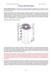
Issue 17 - Free-Energy Devices
Issue 17 - Free-Energy Devices
Issue 17 - Free-Energy Devices

You also want an ePaper? Increase the reach of your titles
YUMPU automatically turns print PDFs into web optimized ePapers that Google loves.
well. The aspect that, according to equation (3),<br />
F tot is zero, is compatible with the fact that the<br />
work of F tot must be equal to zero when the<br />
externally offered energy is equal to zero<br />
(constant voltage and absence of leakages).<br />
However, the equation (3) does not take into<br />
consideration the exact forces which are exerted<br />
on the sum of the charges dq and (dq’), Eq.(6)<br />
takes into account the forces and the<br />
particularities of the boundary conditions<br />
between the surfaces 2 in , 3 out and the dielectric<br />
means 1. At the same time Eq.(6) calculates F tot<br />
on the basis of the simulation being derived if<br />
we assume that the equations (1,2) are in force,<br />
i.e. on the basis of the classic solution of the field<br />
of fig.1 (boundary conditions of constant<br />
voltage on the<br />
elements 3, zero voltage on the casing 2 and<br />
dielectric constant of element 1).<br />
Thus the question is raised of whether the<br />
classical approach, where F tot is zero, or Eq.(6)<br />
where F tot can be non zero, is valid. From Eq.(1)<br />
derives that we have charges in the whole<br />
extend of the dielectric 1 if the potential second<br />
derivative is not zero; this usually is valid in<br />
asymmetrical capacitors<br />
and it can be verified by the aid of finite<br />
elements calculation in various systems and<br />
more specifically in the system proposed as it<br />
will be later described. According to the<br />
classical point of view [Eq.(2)] the charges in<br />
dielectric 1 are virtual and they are used only<br />
for the purposes of the electrostatic field<br />
solution. Obviously this point of view is<br />
arbitrary; therefore Eq.(6) is more consistent<br />
since it takes into account the existing real<br />
charges.<br />
2.2 Specific Arrangement [16]<br />
The specific arrangement proposed is depicted<br />
in Fig.2. The elements 3 (3.1 and 3.2) are formed<br />
by metal deposition (e.g. by means of the “ebeam<br />
evaporation technique”) on the strong<br />
insulation solid dielectrics 1a and 1b, excluding<br />
the surfaces 8, wherein the elements 1a and 1b<br />
are formed by casting<br />
plastic material, e.g. polyethylene. The surfaces<br />
8 may be covered by a mask and using a<br />
technique like lithography, in the case of metal<br />
deposition they can be cleaned and remain<br />
uncovered. On the contrary, all the rest surfaces<br />
New <strong>Energy</strong> Technologies, <strong>Issue</strong> #3 (18) 2004<br />
Fig.2<br />
Zero potential casing asymmetric capacitor system<br />
Specific arrangement<br />
of the sections 1.a and 1.b are covered by a<br />
metallic substance e.g. chrome or nickel. The<br />
sections 1.a and 1.b are joined along the surfaces<br />
8 by an insulation adhesive<br />
forming plates of dimensions e.g. 5 mm x 300<br />
mm x 300 mm. In the case of metal deposition<br />
on dielectric, the developed cohesion is high<br />
enough to exclude the creation of gaps, which<br />
could be the cause of voltage breakdown;<br />
voltage breakdown is also avoided due to the<br />
curvature of the lower parts of element 3. The<br />
metal elements 3 and 2 are connected to the<br />
high voltage ends 11 and 12 through the<br />
conductors 9 and 10, where the conductor 9 is<br />
electrically isolated in such a way that electrical<br />
leakage to be avoided. In this way a thrust is<br />
created mainly due to the electric interaction<br />
of the element 3.1, the element 2.1 and the<br />
interposed dielectric 1a.<br />
We use the method of finite elements for the<br />
arrangement of figure 2 with the following<br />
boundary conditions[16]. The voltage on the<br />
elements 3 is 20.000 V The voltage of the casing<br />
2 is equal to zero. The relative dielectric<br />
constant of the dielectric means 1 is .r=1, The<br />
teeth height of the elements 3 is 2 mm The<br />
minimum distance between the elements 3 and<br />
2.1 is 1 mm The minimum distance between the<br />
75