

MDP - ingot 09 - Freiberg Instruments GmbH
MDP - ingot 09 - Freiberg Instruments GmbH
MDP - ingot 09 - Freiberg Instruments GmbH

Create successful ePaper yourself
Turn your PDF publications into a flip-book with our unique Google optimized e-Paper software.
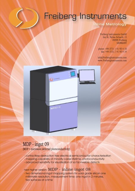
<strong>MDP</strong> - <strong>ingot</strong> <strong>09</strong><br />
(<strong>MDP</strong> = microwave detected photoconductivity)<br />
- contactless destruction free electrical semiconductor characterisation<br />
- mapping capability of minority carrier lifetime, photoconductivity<br />
- advanced sensitivity for visualisation of so far invisible defects<br />
next higher version: <strong>MDP</strong> - inline <strong>ingot</strong> 08<br />
- two dimensional <strong>ingot</strong> mapping system for solar grade silicon one<br />
millimeter resolution, measurement time: one <strong>ingot</strong> in 2 minutes,<br />
two surfaces at a time<br />
<strong>Freiberg</strong> <strong>Instruments</strong> <strong>GmbH</strong><br />
Am St. Niclas Schacht 13<br />
<strong>09</strong>599 <strong>Freiberg</strong><br />
GERMANY<br />
phone: +49 3731 / 41 95 4 10<br />
fax: +49 3731 / 41 95 4 14<br />
info@<strong>Freiberg</strong><strong>Instruments</strong>.com<br />
www.<strong>Freiberg</strong><strong>Instruments</strong>.com
specifications:<br />
- operator modus: quick standard measurement<br />
options<br />
- <strong>ingot</strong> maps and linescans<br />
- parameter autosetting<br />
- F&E modus: highly flexible measurement<br />
parameter setting<br />
samples<br />
- sample: <strong>ingot</strong><br />
- sample size: between 125 x 125 to 210 x 210 mm²<br />
maximum length 500 mm<br />
- resistivity: 0.1 - 10³ Ohm cm<br />
- conduction type: p, n<br />
- material: multi- or monocrystalline silicon<br />
- properties measureable: lifetime (steady state or<br />
non equilibrium(µ-PCD) selectable),<br />
photoconductivity (proportional diffusion length²)<br />
- lifetime range: 0.1 µs - > 100 ms<br />
- excitation power: 200 mW default, 980 nm default<br />
- measurement spot 0.5 mm default<br />
- measurement time depending on sample: for instance<br />
1 mm resolution 156 x 156 mm², 300 mm long: approximately 10 minutes<br />
- tool dimensions: 900 x 600 x 1500 mm<br />
- weight: 100 kg<br />
- power: 110 - 230 V, 50-60 Hz, 8 A max.<br />
PC requirements:<br />
- dual core > 2GHz, >2 GB DDR2, Windows XP 32<br />
or Vista 32<br />
- data transfer, tool to PC via USB2<br />
Software: <strong>MDP</strong> - mapsoft <strong>09</strong><br />
parameter autosetting, access to raw data,<br />
automatic saw criteria output<br />
further tools:<br />
options:<br />
- resistivity map 1 cm² resolution<br />
- p/n equal map 1 mm² resolution<br />
- Barcodescanner<br />
- iron mapping capability<br />
examples: lifetime map multicrystalline silicon <strong>ingot</strong> (upper right), linescan photoconductivity and lifetime (above)<br />
- <strong>MDP</strong> inline: production integrated high speed wafer mapping, suitable for single wafer investigation,<br />
complete two dimensional wafer map at one wafer a second<br />
- <strong>MDP</strong>-map: multipurpose offline tool for flexible contactless electrical material characterisation, lifetime etc.<br />
- <strong>MDP</strong> inline <strong>ingot</strong>: two dimensional <strong>ingot</strong> mapping system for solar grade silicon up<br />
to one millimeter resolution, measurement time: one <strong>ingot</strong> in 2 minutes, two surfaces at a time