DC and low-frequency noise analysis for buried SiGe channel ...
DC and low-frequency noise analysis for buried SiGe channel ... DC and low-frequency noise analysis for buried SiGe channel ...
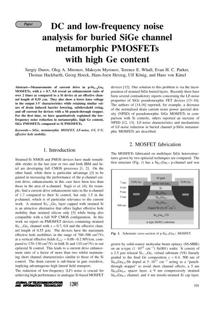
Paper DC and low-frequency noise analysis for buried SiGe channel metamorphic PMOSFETs with high Ge content Sergiy Durov, Oleg A. Mironov, Maksym Myronov, Terence E. Whall, Evan H. C. Parker, Thomas Hackbarth, Georg Hoeck, Hans-Joest Herzog, Ulf König, and Hans von Känel Abstract—Measurements of current drive in p-Si 1−x 1−xGex MOSFETs, with x = 0.7, 0.8 reveal an enhancement ratio of over 2 times as compared to a Si device at an effective channel length of 0.55 µm. They also show a lower knee voltage in the output I-V characteristics while retaining similar values of drain induced barrier lowering, subthreshold swing, and off current for devices with a Sb punch-through stopper. For the first time, we have quantitatively explained the lowfrequency noise reduction in metamorphic, high Ge content, SiGe PMOSFETs compared to Si PMOSFETs. Keywords— SiGe, metamorphic MOSFET, LF-noise, I-V, C-V, effective hole mobility. 1. Introduction Strained-Si NMOS and PMOS devices have made remarkable strides in the last year or two and both IBM and Intel are developing full CMOS processes [1, 2]. On the other hand, while there is particular advantage [3] to be gained in increasing the performance of the p-channel current drive, enhancements in this case have been less than those in the area of n-channel. Sugii et al. [4], for example, find a current drive enhancement ratio in the n-channel of 1.7 compared to their Si control, but only 1.5 in the p-channel, which is of particular relevance to the current work. A strained Si1−xGex layer capped with strained Si is an attractive alternative that offers higher effective hole mobility than strained silicon only [5] while being also compatible with a full N/P CMOS configuration. In this work we report on PMOSFET devices containing strained Si1−xGex channel with x = 0.7, 0.8 and the effective channel length of 0.55 µm. The devices have the maximum effective hole mobilities in the range of 760–500 cm 2 /Vs at a vertical effective fields Ee f f = 0.08−0.2 MV/cm, compared to 170–130 cm 2 /Vs in bulk Si and 110 cm 2 /Vs in our epitaxial Si control. This leads to a current drive enhancement ratio of a factor of more than two whilst maintaining short channel characteristics similar to those of the Si control. The drain current is sub-linear in gate overdrive, implying advantageous high lateral field transport. The reduction of low-frequency (LF) noise is crucial for achieving high performance in analogue Si-based MOSFET devices [12]. One solution to this problem is via the incorporation of strained SiGe buried layers. Recently there have been several contradictory reports concerning the LF-noise properties of SiGe pseudomorphic FET devices [13–16]. The authors of [14,16] reported, for example, a decrease of the normalised drain current noise power spectral density (NPSD) of pseudomorphic SiGe MOSFETs in comparison with Si controls, others reported an increase of NPSD [12, 13]. LF-noise characteristics and mechanisms of LF-noise reduction in buried channel p-SiGe metamorphic MOSFETs are described. 2. MOSFET fabrication The MOSFETs fabricated on multilayer SiGe heterostructures grown by two epitaxial techniques are compared. The first structure (Fig. 1) has a Si0.3Ge0.7 p-channel and was Fig. 1. Schematic cross-section of p-Si0.3Ge0.7 MOSFET. grown by solid-source molecular beam epitaxy (SS-MBE) on an n-type (1 · 10 15 cm −3 ) Si(001) wafer. It consist of a 2.5 µm relaxed Si1−yGey virtual substrate (VS) linearly graded to the final Ge composition y = 0.4, 500 nm of Si0.6Ge0.4:Sb doped at 5 · 10 17 cm −3 acting as a “punchthrough stopper” to avoid short channel effects, a 5 nm Si0.6Ge0.4 spacer layer, a 9 nm compressively strained Si0.3Ge0.7 channel, and 4 nm tensile-strained Si cap layer. 101
- Page 2 and 3: S. Durov, O. A. Mironov, M. Myronov
- Page 4 and 5: S. Durov, O. A. Mironov, M. Myronov
- Page 6 and 7: S. Durov, O. A. Mironov, M. Myronov
- Page 8 and 9: S. Durov, O. A. Mironov, M. Myronov
- Page 10 and 11: S. Durov, O. A. Mironov, M. Myronov
Paper<br />
<strong>DC</strong> <strong>and</strong> <strong>low</strong>-<strong>frequency</strong> <strong>noise</strong><br />
<strong>analysis</strong> <strong>for</strong> <strong>buried</strong> <strong>SiGe</strong> <strong>channel</strong><br />
metamorphic PMOSFETs<br />
with high Ge content<br />
Sergiy Durov, Oleg A. Mironov, Maksym Myronov, Terence E. Whall, Evan H. C. Parker,<br />
Thomas Hackbarth, Georg Hoeck, Hans-Joest Herzog, Ulf König, <strong>and</strong> Hans von Känel<br />
Abstract—Measurements of current drive in p-Si 1−x 1−xGex<br />
MOSFETs, with x = 0.7, 0.8 reveal an enhancement ratio of<br />
over 2 times as compared to a Si device at an effective <strong>channel</strong><br />
length of 0.55 µm. They also show a <strong>low</strong>er knee voltage<br />
in the output I-V characteristics while retaining similar values<br />
of drain induced barrier <strong>low</strong>ering, subthreshold swing,<br />
<strong>and</strong> off current <strong>for</strong> devices with a Sb punch-through stopper.<br />
For the first time, we have quantitatively explained the <strong>low</strong><strong>frequency</strong><br />
<strong>noise</strong> reduction in metamorphic, high Ge content,<br />
<strong>SiGe</strong> PMOSFETs compared to Si PMOSFETs.<br />
Keywords— <strong>SiGe</strong>, metamorphic MOSFET, LF-<strong>noise</strong>, I-V, C-V,<br />
effective hole mobility.<br />
1. Introduction<br />
Strained-Si NMOS <strong>and</strong> PMOS devices have made remarkable<br />
strides in the last year or two <strong>and</strong> both IBM <strong>and</strong> Intel<br />
are developing full CMOS processes [1, 2]. On the<br />
other h<strong>and</strong>, while there is particular advantage [3] to be<br />
gained in increasing the per<strong>for</strong>mance of the p-<strong>channel</strong> current<br />
drive, enhancements in this case have been less than<br />
those in the area of n-<strong>channel</strong>. Sugii et al. [4], <strong>for</strong> example,<br />
find a current drive enhancement ratio in the n-<strong>channel</strong><br />
of 1.7 compared to their Si control, but only 1.5 in the<br />
p-<strong>channel</strong>, which is of particular relevance to the current<br />
work. A strained Si1−xGex layer capped with strained Si<br />
is an attractive alternative that offers higher effective hole<br />
mobility than strained silicon only [5] while being also<br />
compatible with a full N/P CMOS configuration. In this<br />
work we report on PMOSFET devices containing strained<br />
Si1−xGex <strong>channel</strong> with x = 0.7, 0.8 <strong>and</strong> the effective <strong>channel</strong><br />
length of 0.55 µm. The devices have the maximum<br />
effective hole mobilities in the range of 760–500 cm 2 /Vs<br />
at a vertical effective fields Ee f f = 0.08−0.2 MV/cm, compared<br />
to 170–130 cm 2 /Vs in bulk Si <strong>and</strong> 110 cm 2 /Vs in our<br />
epitaxial Si control. This leads to a current drive enhancement<br />
ratio of a factor of more than two whilst maintaining<br />
short <strong>channel</strong> characteristics similar to those of the Si<br />
control. The drain current is sub-linear in gate overdrive,<br />
implying advantageous high lateral field transport.<br />
The reduction of <strong>low</strong>-<strong>frequency</strong> (LF) <strong>noise</strong> is crucial <strong>for</strong><br />
achieving high per<strong>for</strong>mance in analogue Si-based MOSFET<br />
devices [12]. One solution to this problem is via the incorporation<br />
of strained <strong>SiGe</strong> <strong>buried</strong> layers. Recently there have<br />
been several contradictory reports concerning the LF-<strong>noise</strong><br />
properties of <strong>SiGe</strong> pseudomorphic FET devices [13–16].<br />
The authors of [14,16] reported, <strong>for</strong> example, a decrease<br />
of the normalised drain current <strong>noise</strong> power spectral density<br />
(NPSD) of pseudomorphic <strong>SiGe</strong> MOSFETs in comparison<br />
with Si controls, others reported an increase of<br />
NPSD [12, 13]. LF-<strong>noise</strong> characteristics <strong>and</strong> mechanisms<br />
of LF-<strong>noise</strong> reduction in <strong>buried</strong> <strong>channel</strong> p-<strong>SiGe</strong> metamorphic<br />
MOSFETs are described.<br />
2. MOSFET fabrication<br />
The MOSFETs fabricated on multilayer <strong>SiGe</strong> heterostructures<br />
grown by two epitaxial techniques are compared. The<br />
first structure (Fig. 1) has a Si0.3Ge0.7 p-<strong>channel</strong> <strong>and</strong> was<br />
Fig. 1. Schematic cross-section of p-Si0.3Ge0.7 MOSFET.<br />
grown by solid-source molecular beam epitaxy (SS-MBE)<br />
on an n-type (1 · 10 15 cm −3 ) Si(001) wafer. It consist of<br />
a 2.5 µm relaxed Si1−yGey virtual substrate (VS) linearly<br />
graded to the final Ge composition y = 0.4, 500 nm of<br />
Si0.6Ge0.4:Sb doped at 5 · 10 17 cm −3 acting as a “punchthrough<br />
stopper” to avoid short <strong>channel</strong> effects, a 5 nm<br />
Si0.6Ge0.4 spacer layer, a 9 nm compressively strained<br />
Si0.3Ge0.7 <strong>channel</strong>, <strong>and</strong> 4 nm tensile-strained Si cap layer.<br />
101
S. Durov, O. A. Mironov, M. Myronov, T. E. Whall, E. H. C. Parker, T. Hackbarth, G. Hoeck, H.-J. Herzog, U. König, <strong>and</strong> H. von Känel<br />
Fig. 2. Schematic cross-section of p-Si0.2Ge0.8 MOSFET.<br />
The second structure (Fig. 2) was grown by <strong>low</strong> energy<br />
plasma enhanced CVD (LEPECVD) <strong>and</strong> differs in that the<br />
VS terminates at y = 0.5, there is no punch through stopper<br />
<strong>and</strong> the p-<strong>channel</strong> is 7 nm of strained Si0.2Ge0.8. As<br />
x−y = 0.3 in both structures the strain in the p-<strong>channel</strong> will<br />
be the same. The PMOSFET devices were fabricated using<br />
reduced thermal budget processing at 650 ◦ C, to minimize<br />
Ge out-diffusion from the strained Si1−xGex <strong>channel</strong> [7]<br />
<strong>and</strong> to avoid Sb penetration to the <strong>channel</strong>, with 200 nm of<br />
plasma enhanced CVD (PECVD) SiO2 deposited as a field<br />
oxide. In the active transistor area the field oxide was removed<br />
by wet chemical etching. After a cleaning step the<br />
gate oxide on the first SS-MBE grown structure was deposited<br />
by remote plasma enhanced CVD (RPECVD) as<br />
a 7 nm SiO2 layer at 300 ◦ C [18]. The gate oxide on the<br />
second LEPECVD grown structure was 8.5 nm PECVD<br />
deposited at 370 ◦ C, fol<strong>low</strong>ed by annealing in a N2O atmosphere<br />
at 650 ◦ C <strong>for</strong> 1 min. Source <strong>and</strong> drain contacts were<br />
fabricated by BF2 + implantation at 40 keV, with a dose<br />
of 4·10 15 cm −2 <strong>and</strong> activated at 650 ◦ C <strong>for</strong> 30 s. The surface<br />
of contact areas was etched <strong>for</strong> a short time to remove<br />
impurities increasing contact resistance. Finally, the Al<br />
gate <strong>and</strong> Ti/Pt/Au contact metallization were evaporated.<br />
The second p-Si0.2Ge0.8(2) device of Table 1 was made<br />
using the same process as <strong>for</strong> MBE-grown p-Si0.3Ge0.7 device<br />
[5], but the thickness of the SiO2 layer is 11 nm.<br />
The p-Si MOSFET devices were fabricated on SS-MBE<br />
grown 100 nm Si epilayer, grown on n-type (1·10 17 cm −3 )<br />
Table 1<br />
Electrical <strong>and</strong> structural properties of 0.55 µm<br />
p-Si0.3Ge0.7, p-Si0.2Ge0.8 <strong>and</strong> p-Si MOSFETs<br />
Parameter Si Si0.3Ge0.7 Si0.2Ge0.8 Si0.2Ge0.8 (2)<br />
SiO2 thickness [nm] 9 7 8.5 11<br />
g m (sat) [mS/mm] 40 84 95 63<br />
S [mV/decade] 85 95 130 200<br />
VT H [V] –0.2 –0.84 –0.26 –0.95<br />
ION/IOFF<br />
[VDS = −50 mV]<br />
ION/IOFF<br />
[VDS = −3 V]<br />
102<br />
10 6 10 6 2.5 · 10 3 2.5 · 10 3<br />
10 4 10 4 15 26<br />
Si(001) wafers using a self-aligned gate process, with 9 nm<br />
dry SiO2 thermally grown at 800 ◦ C <strong>for</strong> 120 min <strong>and</strong> 300 nm<br />
p-type (5·10 19 cm −3 ) poly-Si gate. The row of geometrical<br />
gate lengths <strong>for</strong> all fabricated transistors was in the range<br />
L = 0.4−50 µm with the same gate width W = 50 µm.<br />
3. <strong>DC</strong> characteristics<br />
Current-voltage (I-V) <strong>and</strong> quasistatic capacitance-voltage<br />
(C-V) characteristics were measured using an Agilent<br />
4156C parameter analyzer <strong>for</strong> all devices at a temperature<br />
of 293 K (the basic parameters are given in Table 1). The<br />
input I-V characteristics <strong>for</strong> the Si0.3Ge0.7 PMOSFET in<br />
Fig. 3 show reduced drain induced barrier <strong>low</strong>ering (DIBL)<br />
Fig. 3. Input I-V characteristics <strong>for</strong> p-Si0.3Ge0.7 MOSFET with<br />
Le f f = 0.55 µm.<br />
<strong>and</strong> an excellent subthreshold swing S = 95 mV/decade<br />
at VDS = −50 mV, which demonstrates the efficiency<br />
of the “punch-through stopper” <strong>for</strong> sub-micron MOSFET<br />
operation. This device has an excellent ION/IOFF ratio<br />
of 10 6 in the linear region (VDS = −50 mV) <strong>and</strong> in saturation<br />
(VDS = −3 V) ION/IOFF ≈ 10 4 . The threshold voltage<br />
VT H is -0.84 V at VDS = −50 mV.<br />
The input I-V characteristics <strong>for</strong> the p-Si MOSFET are<br />
shown in Fig. 4. In this case, the subthreshold swing is<br />
85 mV/decade <strong>and</strong> ION/IOFF is 10 6 in the linear region<br />
<strong>and</strong> 10 4 in saturation. The threshold voltage VT H is –0.2 V.<br />
Comparison of these two devices shows the metamorphic<br />
MOSFET is operating in an acceptable way <strong>and</strong> provides<br />
a competitive device at this technology node. The slight<br />
increase in S in the p-Si0.3Ge0.7 device can be completely<br />
accounted <strong>for</strong> by the added capacitance of the strained Si<br />
overlayer.<br />
The electrical characteristics of the p-Si0.2Ge0.8 MOS-<br />
FET, which does not have a punch through stopper, are
Fig. 4. Input I-V characteristics <strong>for</strong> p-Si MOSFET with Le f f =<br />
0.55 µm.<br />
Fig. 5. Output I-V characteristics of p-Si <strong>and</strong> p-Si0.3Ge0.7<br />
MOSFET with Le f f = 0.55 µm at the same VG–VT H.<br />
not as impressive. The subthreshold slope is increased<br />
to 130 mV/decade <strong>and</strong> the device does not switch off<br />
well resulting in a much reduced ION/IOFF ratio. This is<br />
a consequence of the vertical architecture not being optimised<br />
<strong>for</strong> sub-micron device operation rather than any inherent<br />
problem with the <strong>channel</strong> material, as will be seen<br />
in the mobility measurements <strong>and</strong> output characteristics<br />
be<strong>low</strong>.<br />
<strong>DC</strong> <strong>and</strong> <strong>low</strong>-<strong>frequency</strong> <strong>noise</strong> <strong>analysis</strong> <strong>for</strong> <strong>buried</strong> <strong>SiGe</strong> <strong>channel</strong> metamorphic PMOSFETs with high Ge content<br />
Fig. 6. Output I-V characteristics of p-Si <strong>and</strong> p-Si0.2Ge0.8 MOS-<br />
FET with Le f f = 0.55 µm at the same VG–VT H.<br />
Fig. 7. Kink effect on output I-V characteristics of p-Si0.3Ge0.7<br />
at <strong>low</strong> temperatures T = 77 K.<br />
The maximum transconductance in the saturation region<br />
is gm = 84 <strong>and</strong> 95 mS/mm respectively compared to<br />
40 mS/mm in the Si control. The maximum drain current<br />
at VG −VT H = −2.5 V is 165 mA/mm <strong>for</strong> p-Si0.3Ge0.7 <strong>and</strong><br />
230 mA/mm <strong>for</strong> p-Si0.2Ge0.8.<br />
The output I-V characteristics measured on both the<br />
p-Si0.3Ge0.7 <strong>and</strong> p-Si0.2Ge0.8 MOSFETs are shown in Fig. 5<br />
<strong>and</strong> Fig. 6, with comparisons to the p-Si device. Enhance-<br />
103
S. Durov, O. A. Mironov, M. Myronov, T. E. Whall, E. H. C. Parker, T. Hackbarth, G. Hoeck, H.-J. Herzog, U. König, <strong>and</strong> H. von Känel<br />
ment in the saturated drain current by a factor of 2.5–3<br />
is clearly visible in the output I-V characteristics of the<br />
Si0.3Ge0.7 PMOSFET (Fig. 5) at VDS = −2.5 V, in comparison<br />
with the silicon control. Similar enhancement is seen<br />
at all values of drain bias. For the Si0.2Ge0.8 PMOSFET<br />
the enhancement factor in the normalised saturation drain<br />
current is actually higher than <strong>for</strong> the Si0.3Ge0.7 PMOSFET<br />
<strong>and</strong> is more than a factor of three above the control.<br />
The I-V characteristics of the p-Si0.2Ge0.8(2) MOSFET are<br />
similar to those of p-Si0.2Ge0.8 MOSFET <strong>and</strong> differ only<br />
in slightly <strong>low</strong>er drain current values due to thicker gate<br />
dielectric.<br />
The self-heating effect, which is responsible <strong>for</strong> the mobility<br />
degradation, threshold voltage <strong>low</strong>ering <strong>and</strong> negative<br />
differential conductance, was observed in all high Ge<br />
content metamorphic <strong>SiGe</strong> MOSFETs with gate length be<strong>low</strong><br />
2 µm at high VDS. The “kink” effect (Fig. 7) was<br />
clearly observed at <strong>low</strong> temperature (77 K) <strong>for</strong> devices with<br />
a punch-through stopper (p-Si0.3Ge0.7). This is due to the<br />
majority carriers generated by impact ionization that are<br />
collected in the body <strong>and</strong> increase the body potential (<strong>low</strong>er<br />
threshold voltage). For devices without a punch-through<br />
stopper (p-Si0.2Ge0.8) the “kink” effect was not observed.<br />
This behavior of our devices is similar to partially depleted<br />
silicon-on-insulator (SOI) MOSFETs [10].<br />
Fig. 8. Drain current ID (thick lines) <strong>and</strong> transconductance gm<br />
(thin lines) versus gate voltage <strong>for</strong> p-Si0.3Ge0.7 (solid lines) <strong>and</strong><br />
p-Si (dashed lines) MOSFETs with effective gate length 0.55 µm<br />
at room (T = 293 K) <strong>and</strong> nitrogen (T = 77 K) temperatures.<br />
The <strong>low</strong> temperature measurements have been carried out<br />
in liquid nitrogen (T = 77 K). The input I-V characteristics<br />
<strong>for</strong> the p-Si0.3Ge0.7 MOSFET at T = 77 K in comparison<br />
with the characteristics obtained at room temperature<br />
T = 293 K are shown in Fig. 8. The threshold voltage VT H<br />
increases slightly with the temperature decreasing to 77 K.<br />
The maximum transconductance gm <strong>and</strong> maximum drain<br />
current ID in the linear regime increased 2.8 <strong>and</strong> 1.6 times,<br />
104<br />
respectively, at 77 K when compared to the corresponding<br />
values measured at 293 K. The maximum transconductance<br />
gm <strong>and</strong> maximum drain current ID in saturation<br />
increased 1.4 <strong>and</strong> 1.3 times, respectively, at 77 K when<br />
compared to the respective values measured at 293 K.<br />
The C-V characteristics were measured on devices with<br />
gate length L = 50 µm <strong>and</strong> gate width W = 50 µm.<br />
The p-Si0.2Ge0.8(2) MOSFETs with gate oxide thickness<br />
of 11 nm operate at the gate voltage range −6 V ≤VG ≤ 6 V<br />
be<strong>for</strong>e breakdown. Figure 9 clearly shows that the Si cap<br />
starts to fill with carriers only at a gate overdrive volt-<br />
Fig. 9. High <strong>frequency</strong> split C-V characteristics <strong>for</strong> MOSFET<br />
p-Si0.2Ge0.8(2) with effective gate length 50 µm at room temperature<br />
293 K (solid lines) <strong>and</strong> at liquid nitrogen temperature 77 K<br />
(dashed lines).<br />
age of 3.5 V. Very small changes in C-V curves measured<br />
at 77 K <strong>and</strong> at 293 K indicate <strong>low</strong> level of impurities in<br />
the heterostructure <strong>and</strong> <strong>low</strong> concentration of mobile charge<br />
inside the gate dielectric.<br />
The C-V characteristics <strong>for</strong> p-Si0.3Ge0.7 MOSFETs with<br />
SiO2 thickness of 7 nm (Fig. 10) show that the Si cap<br />
is not filled up to 2 V gate overdrive voltage. The oxide<br />
breakdown limit <strong>for</strong> p-Si0.3Ge0.7 devices is around 4 V.<br />
The depletion charge was extracted from quasistatic <strong>and</strong><br />
high <strong>frequency</strong> C-V characteristics [11]. Figure 11 shows<br />
increasing of the depletion charge <strong>for</strong> p-Si0.3Ge0.7 heterostructure<br />
from the depth of 25 nm. The value of the<br />
depletion charge is ∼ 3 · 10 17 cm −3 at maximum. It corresponded<br />
to the n-type doped <strong>SiGe</strong> buffer layer of 15 nm<br />
thickness that lays 5 nm beneath the <strong>channel</strong>. The depletion<br />
charge curve is broken abruptly at the depth of<br />
40 nm, which points to a limitation of the depletion approximation.<br />
The depletion regime is changed to the inversion<br />
regime (holes accumulation) at this depth. No peculiarity<br />
was observed on the depletion charge curves <strong>for</strong>
Fig. 10. High <strong>frequency</strong> (solid line) <strong>and</strong> quasistatic (dots)<br />
C-V characteristics <strong>for</strong> MOSFET p-Si0.3Ge0.7 with effective gate<br />
length 50 µm at room temperature.<br />
Fig. 11. Depletion charge profiles extracted from quasistatic <strong>and</strong><br />
high <strong>frequency</strong> C-V characteristics <strong>for</strong> p-Si0.3Ge0.7, p-Si0.2Ge0.8,<br />
<strong>and</strong> p-Si0.2Ge0.8(2) heterostructures.<br />
p-Si0.2Ge0.8 <strong>and</strong> p-Si0.2Ge0.8(2) MOSFETs. This indicates<br />
that the under-<strong>channel</strong> area of these samples was not doped<br />
or was doped with background donor concentration less<br />
than 1·10 16 cm −3 . Also Fig. 11 shows <strong>low</strong>er impurity background<br />
of the p-Si0.2Ge0.8(2) heterostructure when compared<br />
to the p-Si0.2Ge0.8 heterostructure.<br />
The effective mobility µe f f (Fig. 12) has been determined<br />
as a function of Ee f f on large area MOSFETs (gate width W<br />
<strong>and</strong> length L both equal to 50 µm), from the input I-V at<br />
<strong>DC</strong> <strong>and</strong> <strong>low</strong>-<strong>frequency</strong> <strong>noise</strong> <strong>analysis</strong> <strong>for</strong> <strong>buried</strong> <strong>SiGe</strong> <strong>channel</strong> metamorphic PMOSFETs with high Ge content<br />
<strong>low</strong> VDS = −50 mV <strong>and</strong> from quasistatic <strong>and</strong> high <strong>frequency</strong><br />
split C-V characteristics [11]. 1D Poisson-Schrodinger simulation<br />
was used to obtain correct sheet densities inside the<br />
structure <strong>and</strong> recheck the parameters extracted from the depletion<br />
approximation by fitting the measured C-V data.<br />
Fig. 12. Effective mobility as a function of effective field <strong>for</strong><br />
p-Si0.3Ge0.7, p-Si0.2Ge0.8, p-Si0.2Ge0.8(2) <strong>and</strong> p-Si MOSFETs,<br />
as well as universal curves <strong>for</strong> p-Si MOS <strong>and</strong> n-Si MOS after<br />
S. Takagi [9].<br />
The p-Si0.2Ge0.8(2) heterostructure has the highest mobility<br />
760 cm 2 V −1 s −1 at the field Ee f f = 0.08 MV/cm<br />
due to the <strong>low</strong>est background of ionized impurities. On<br />
the other h<strong>and</strong>, p-Si0.2Ge0.8(2) MOSFETs have the worst<br />
subthreshold slope, that could be explained by MOS-<br />
FET short <strong>channel</strong> effects due to the absence of n-type<br />
“punch through” stopper (ionized impurities) underneath of<br />
p-Si0.2Ge0.8 <strong>channel</strong>.<br />
4. Low-<strong>frequency</strong> <strong>noise</strong><br />
Conventional MOSFET characterisation techniques, such<br />
as the combination of I-V (current-voltage) <strong>and</strong> C-V (capacitance-voltage)<br />
measurements, are very problematic as<br />
device size decreases down to the deep sub-µm (DS-µm)<br />
scale. “Average per square” characteristic parameters obtained<br />
from large-scale devices cannot be suitable <strong>for</strong><br />
DS-µm MOSFET <strong>analysis</strong> due to statistical uncertainty of<br />
fabrication technology together with the importance of<br />
mesoscopic quantum effects. Low-<strong>frequency</strong> <strong>noise</strong> measurements<br />
could be a powerful diagnostic technique <strong>for</strong> DS-µm<br />
MOSFET characterization in a wide range of device operation<br />
regimes [17]. Un<strong>for</strong>tunately, the commercially available<br />
current preamplifiers such as ITHACO-1211, SR-570,<br />
EG&G-181 have been optimised only <strong>for</strong> limited ranges<br />
105
S. Durov, O. A. Mironov, M. Myronov, T. E. Whall, E. H. C. Parker, T. Hackbarth, G. Hoeck, H.-J. Herzog, U. König, <strong>and</strong> H. von Känel<br />
Fig. 13. Schematic of the current preamplifier with modular design <strong>and</strong> interchangeable first stage <strong>for</strong> LF-<strong>noise</strong> measurements.<br />
of device input impedance <strong>and</strong> their conventional “all-inone”<br />
desktop design also introduces extra problems when<br />
long cables are used to connect the equipment to the sample<br />
test fixture. To overcome all the above problems we<br />
have used the optimised preamplifier modules as the first<br />
stages <strong>for</strong> gate leakage <strong>and</strong> drain current <strong>noise</strong> measurements<br />
of MOSFETs with input impedance 50 Ω–10 8 Ω<br />
in the <strong>frequency</strong> range of 1.0 Hz–10 5 Hz. A three-box<br />
modular design with interchangeable first stage preamplifiers<br />
(Fig. 13) was chosen to improve the reliability <strong>and</strong> to<br />
reduce the influence of the connection cables on measurement<br />
results. The best operational amplifiers (OAMPs) currently<br />
available with optimal voltage vn <strong>and</strong> current in <strong>noise</strong>,<br />
AD549 (vn = 200 nV Hz −1/2 , in = 0.15 fAHz −1/2 ), OPA637<br />
(vn = 3.7 nVHz −1/2 , in = 2.0 fAHz −1/2 ) <strong>and</strong> LT1028A<br />
(vn = 0.85 nVHz −1/2 , in = 1.0 pAHz −1/2 ) were used <strong>for</strong> the<br />
first stage module at each of the three chosen impedance<br />
ranges.<br />
The LF-<strong>noise</strong> was measured using an HP 35670A dynamic<br />
signal analyzer <strong>and</strong> the custom-made preamplifier described<br />
above. Characteristics I-V <strong>and</strong> LF-<strong>noise</strong> were measured simultaneously<br />
to account <strong>for</strong> possible offset of the applied<br />
gate voltage VG. All measurements were done on MOS-<br />
FETs with a geometrical gate length of 1.0 µm (an effective<br />
gate length was extracted as 0.55 µm) <strong>and</strong> 10 µm in<br />
an electrically shielded room at 293 K. The <strong>SiGe</strong> MOS-<br />
FETs show enhancement in the drain current <strong>and</strong> transconductance<br />
at the same gate overdrive voltages in comparison<br />
with p-Si devices. LF-<strong>noise</strong> has been measured in the linear<br />
106<br />
regime of the output I-V characteristics (VDS = −50 mV),<br />
from the sub-threshold through weak to strong inversion<br />
(VG −VT H from 0.5 to −3 V) of the input I-V, in a wide<br />
range of drain-source conductance gd = ID/VDS.<br />
Fig. 14. Normalized power spectral density of drain current fluctuations<br />
as a function of <strong>frequency</strong> <strong>for</strong> p-Si0.3Ge0.7 , p-Si0.2Ge0.8<br />
<strong>and</strong> p-Si MOSFETs.
A typical normalized power spectral density (NPSD) SI/I2 of drain current fluctuations versus <strong>frequency</strong> in the<br />
range 1–105 Hz is presented in Fig. 14. Flicker, 1/ f component,<br />
at <strong>low</strong> frequencies <strong>and</strong> thermal <strong>noise</strong> at high <strong>frequency</strong><br />
range, dominate the spectra. In Fig. 14 the 1/ f <strong>noise</strong><br />
<strong>for</strong> the p-Si0.3Ge0.7 MOSFET is clearly seen to be over<br />
three times <strong>low</strong>er than that <strong>for</strong> Si. We have not observed<br />
a generation-recombination (GR) <strong>noise</strong> component at any<br />
gate overdrive voltage. This is usually manifested as bumps<br />
in the spectra. GR <strong>noise</strong> could appear in the spectra due to<br />
Sb diffusion into the Si0.3Ge0.7 <strong>channel</strong> from the Sb-doped<br />
“punch-through” stopper or the existence of deep levels in<br />
the heterostructure. Thus we can confirm the absence of<br />
these defects <strong>and</strong> contaminations after the full MOSFET<br />
fabrication process.<br />
The NPSD SID<br />
<strong>DC</strong> <strong>and</strong> <strong>low</strong>-<strong>frequency</strong> <strong>noise</strong> <strong>analysis</strong> <strong>for</strong> <strong>buried</strong> <strong>SiGe</strong> <strong>channel</strong> metamorphic PMOSFETs with high Ge content<br />
in the 1/ f region is described in terms of<br />
carrier number fluctuations (CNF), correlated mobility fluctuations<br />
(CMF) <strong>and</strong> source-drain series resistance fluctuations<br />
(SDRF) [17]:<br />
SID /I2 D = 2 1 + αµe f fC ID/gm<br />
2 2 gm ID<br />
Sv + SRSD f b<br />
ID VDS<br />
,<br />
where α is the Coulomb scattering coefficient, µe f f is<br />
the effective mobility, SV f b = SQit /(WLC2 ) with SQit being<br />
the interface charge spectral density per unit area, C is<br />
the gate oxide capacitance Cox.<br />
The flat b<strong>and</strong> voltage spectral density is defined by [17]:<br />
SV = f b Q2kBT Nst<br />
WLC 2 ox f γ = q2kBT λNt<br />
WLC 2 ox f<br />
(1)<br />
γ , (2)<br />
where f is the <strong>frequency</strong>, γ is the characteristic exponent<br />
close to unity, kBT is the thermal energy, Nst is the density<br />
of traps near the Si/SiO2 <strong>and</strong>/or Si/<strong>SiGe</strong> interface, λ is<br />
the tunnel attenuation distance to Si cap <strong>and</strong>/or SiO2, <strong>and</strong><br />
Nt is the volumetric trap density in the Si cap <strong>and</strong>/or SiO2.<br />
The spectral density of the source-drain series resistance<br />
we defined by:<br />
SRSD = αH<br />
R<br />
SD<br />
2 SD<br />
f NSD<br />
∼ R3 SD<br />
f<br />
, (3)<br />
where αH SD is the Hooge parameter <strong>for</strong> 1/ f <strong>noise</strong> in the<br />
series resistance, NSD is the total number of free carriers<br />
<strong>and</strong> RSD is the source-drain series resistance.<br />
The CMF can be important in both the weak <strong>and</strong> strong<br />
inversion regions of MOSFET operation. Typically, SDRF<br />
can appear at the highest gate voltages <strong>for</strong> the shortest <strong>channel</strong><br />
lengths, when the <strong>channel</strong> resistance becomes comparable<br />
to the source-drain series resistance.<br />
Figure 15 shows how measured <strong>and</strong> calculated power spectral<br />
density (PSD) varies with device conductance <strong>for</strong> the<br />
p-Si MOSFET. This curve was very well fitted by CNF,<br />
CMF <strong>and</strong> SDRF using Eq. (1). The Coulomb scattering<br />
coefficient α = 8 · 10 4 Vs/C extracted from the fitting<br />
of the experimental data <strong>for</strong> p-Si MOSFET is close<br />
to the predicted value of 10 5 Vs/C <strong>for</strong> holes [17]. It is<br />
comparable to α PM Si cap <strong>for</strong> the Si cap of pseudomorphic<br />
p-<strong>SiGe</strong> devices <strong>and</strong> much higher than that <strong>for</strong> <strong>SiGe</strong><br />
<strong>channel</strong>s of the same pseudomorphic p-<strong>SiGe</strong> MOSFETs<br />
α PM <strong>SiGe</strong> =∼0.1α PM Si cap [12].<br />
Fig. 15. Power spectral density dependence on device conductance<br />
<strong>for</strong> p-Si MOSFET.<br />
Fig. 16. Power spectral density dependence on device conductance<br />
<strong>for</strong> p-Si0.3Ge0.7 MOSFET.<br />
Figures 16 <strong>and</strong> 17 show the variation of PSD with device<br />
conductance <strong>for</strong> the p-Si0.3Ge0.7 <strong>and</strong> p-Si0.2Ge0.8<br />
MOSFETs, respectively.<br />
107
S. Durov, O. A. Mironov, M. Myronov, T. E. Whall, E. H. C. Parker, T. Hackbarth, G. Hoeck, H.-J. Herzog, U. König, <strong>and</strong> H. von Känel<br />
The variation is explained completely by CNF <strong>and</strong> SDRF,<br />
which reduce Eq. (1) <strong>for</strong> the NPSD to:<br />
SID /I2 D =<br />
2 2 gm<br />
ID<br />
SV + f b<br />
ID VDS<br />
SRSD . (4)<br />
In the case of our metamorphic p-<strong>SiGe</strong> MOSFETs the CMF<br />
component was not observed (α
<strong>for</strong> p-<strong>SiGe</strong> MOSFETs. This could be explained by the difference<br />
in Si <strong>and</strong> <strong>SiGe</strong> fabrication technologies. The quality<br />
of SiO2 <strong>for</strong> p-<strong>SiGe</strong> MOSFETs is worse, due to the <strong>low</strong>er<br />
thermal budget required <strong>for</strong> the whole processing. Also,<br />
average densities of traps λNt extracted from LF-<strong>noise</strong> are<br />
less than values usually obtained from C-V characteristics.<br />
This could be explained if it is assumed that either not all<br />
the traps inside SiO2 are involved in the trapping-detrapping<br />
process or other processes also affect the LF-<strong>noise</strong>.<br />
5. Conclusions<br />
In conclusion, all these results demonstrate the advantages<br />
of metamorphic MOSFETs with a high Ge content <strong>and</strong><br />
strained Si1−xGex p-<strong>channel</strong> grown on a relaxed Si1−yGey<br />
buffer in comparison with a bulk p-Si MOSFET. Both<br />
SS-MBE <strong>and</strong> LEPECVD grown material shows very significant<br />
hole mobility improvement over bulk Si, with peak<br />
values of µe f f = 760 cm 2 V −1 s −1 . Of the three types devices<br />
studied the SS-MBE grown Si0.3Ge0.7 structure produces<br />
the best per<strong>for</strong>mance as a sub-micron MOSFET<br />
device, mainly due to the incorporation of an Sb-doped<br />
punch-through stopper. This results in a <strong>SiGe</strong> device with<br />
similar to the Si control short <strong>channel</strong> properties at an effective<br />
<strong>channel</strong> length of 0.55 µm to the Si control. The<br />
current drive enhancement ratio of 2.0 over p-Si MOS-<br />
FET is found in the p-Si0.3Ge0.7 MOSFET, <strong>and</strong> is due<br />
to higher hole mobility µe f f = 500 cm 2 V −1 s −1 in the<br />
Si0.3Ge0.7 quantum well. The highest drive current is found<br />
in the p-Si0.2Ge0.8 MOSFET, with a current drive enhancement<br />
ratio of more than 3.0 over the p-Si MOSFET. These<br />
studies demonstrate clearly the potential of using strained<br />
Si0.3Ge0.7 <strong>and</strong> Si0.2Ge0.8 heterostructures <strong>for</strong> the PMOS-<br />
FETs in CMOS structure.<br />
Also, the results presented in this paper demonstrate a significant<br />
reduction in LF-<strong>noise</strong> NPSD, achieved in metamorphic<br />
p-Si0.3Ge0.7 <strong>and</strong> p-Si0.2Ge0.8 MOSFETs compared<br />
to bulk p-Si. This advantage is observed in sub-micron<br />
devices relevant to the current Si-CMOS technology. In<br />
the linear region of MOSFET operation the reduction in<br />
1/ f <strong>noise</strong> is higher than a factor of three. The reduction<br />
is attributed to the existence of the Si cap layer in<br />
the p-<strong>SiGe</strong> MOSFETs, which further separates the holes<br />
in the <strong>buried</strong> Si0.3Ge0.7 <strong>and</strong> Si0.2Ge0.8 <strong>channel</strong>s from the<br />
traps near the Si/SiO2 interface, <strong>and</strong> an immeasurably <strong>low</strong><br />
influence of traps at the Si/<strong>SiGe</strong> interface. LF-<strong>noise</strong> per<strong>for</strong>mance<br />
of p-<strong>SiGe</strong> MOSFETs could be significantly improved<br />
after technology of gate dielectric fabrication will be<br />
improved.<br />
The influence of a “punch-through” stopper on the device<br />
reliability was analysed. It reduces short <strong>channel</strong> effects in<br />
sub-micron developed MOSFETs <strong>and</strong> provides perfect per<strong>for</strong>mance<br />
of devices especially in the subthreshold region<br />
as it is most important <strong>for</strong> switching devices (CMOS logic).<br />
Also 1/ f <strong>noise</strong> is not significantly increased in <strong>buried</strong> <strong>channel</strong><br />
p-<strong>SiGe</strong> devices with a “punch-through” stopper as in<br />
conventional p-Si MOSFETs with heavily doped substrate<br />
<strong>DC</strong> <strong>and</strong> <strong>low</strong>-<strong>frequency</strong> <strong>noise</strong> <strong>analysis</strong> <strong>for</strong> <strong>buried</strong> <strong>SiGe</strong> <strong>channel</strong> metamorphic PMOSFETs with high Ge content<br />
due to a 4–5 nm Si cap used. On the other h<strong>and</strong>, the introduced<br />
“punch-through” stopper slightly decreases the maximum<br />
current of the device <strong>and</strong> increases the influence of<br />
the negative effects due to impact ionization in the drain<br />
depletion area. These effects could be reduced through<br />
the optimization of the contact shape <strong>and</strong> doping profile.<br />
Better results could possibly be obtained using p-<strong>SiGe</strong><br />
<strong>buried</strong> <strong>channel</strong> heterostructures together with SOI technology<br />
(analogue of fully depleted SOI MOSFETs [10]).<br />
References<br />
[1] K. Rim et al., “Characteristics <strong>and</strong> device design of sub-100 nm<br />
strained Si N- <strong>and</strong> PMOSFETs”, in Symp. VLSI Technol., Honolulu,<br />
USA, 2002, pp. 98–99.<br />
[2] S. Thompson et al., “A 90 nm logic technology featuring 50 nm<br />
strained silicon <strong>channel</strong> transistors”, IEDM, p. 50, 2002.<br />
[3] A. Sadek, K. Ismail, M. A. Armstrong, D. A. Antoniadis,<br />
<strong>and</strong> F. Stern, “Design of Si/<strong>SiGe</strong> heterojunction complementary<br />
metal-oxide-semiconductor transistors”, IEEE Trans. Electron Dev.,<br />
vol. 43, no. 8, pp. 1224–1232, 1996.<br />
[4] N. Sugii, D. Hisamoto, K. Washio, N. Yokoyama, <strong>and</strong> S. Kimura,<br />
“Per<strong>for</strong>mance enhancement of strained-Si MOSFETs fabricated on<br />
a chemical-mechanical-polished <strong>SiGe</strong> substrate”, IEEE Trans. Electron<br />
Dev., vol. 49, no. 12, pp. 2237–2243, 2002.<br />
[5] G. Höck, E. Kohn, C. Rosenblad, H. von Känel, H.-J. Herzog, <strong>and</strong><br />
U. König, “High hole mobility in Si0.17Ge0.83 <strong>channel</strong> metal-oxidesemiconductor<br />
field-effect transistors grown by plasma-enhanced<br />
chemical vapor deposition”, Appl. Phys. Lett., vol. 76, no. 26,<br />
pp. 3920–3922, 2000.<br />
[6] C. W. Leitz, M. T. Currie, M. L. Lee, Z.-Y. Cheng, D. A. Antoniadis,<br />
<strong>and</strong> E. A. Fitzgerald, “Hall mobility enhancement in strained<br />
Si/Si1−yGey p-type metal-oxide-semiconductor field-effect transistors<br />
grown on relaxed Si1−xGex (x < y) virtual substrates”, Appl.<br />
Phys. Lett., vol. 79, no. 25, pp. 4246–4248, 2001.<br />
[7] M. Myronov, P. J. Phillips, T. E. Whall, <strong>and</strong> E. H. C Parker,<br />
“Hall mobility enhancement caused by annealing of<br />
Si0.2Ge0.8/Si0.7Ge0.3/Si(001) p-type modulation-doped heterostructures”,<br />
Appl. Phys. Lett., vol. 80, pp. 3557–3559, 2002.<br />
[8] T. Koster, J. Stein, B. Hadam, J. Gondermann, B. Spangenberg,<br />
H. G. Roskos, H. Kurz, M. Holzmann, M. Riedinger, <strong>and</strong> G. Abstreiter,<br />
“Fabrication <strong>and</strong> characterisation of <strong>SiGe</strong> based in-plane-gate<br />
transistors”, Microelectron. Eng., vol. 35, no. 1–4, pp. 301–304,<br />
1997.<br />
[9] S. Takagi, A. Toriumi, M. Iwase, <strong>and</strong> H. Tango, “On the universality<br />
of inversion layer mobility in Si MOSFET’s: Part I – Effects of substrate<br />
impurity concentration”, IEEE Trans. Electron Dev., vol. 41,<br />
pp. 2351–2356, 1994.<br />
[10] S. Cristoloveanu, “Silicon on insulator technologies <strong>and</strong> devices:<br />
from present to future”, Solid-State Electron., vol. 45,<br />
pp. 1403–1411, 2001.<br />
[11] D. K. Schroder, Semiconductor Material <strong>and</strong> Device Characterization.<br />
2nd ed. Wiley, 1998, pp. 540–547.<br />
[12] G. Ghibaudo <strong>and</strong> J. Chroboczek, “On the origin of the LF <strong>noise</strong> in<br />
Si/Ge MOSFETs”, Solid-State Electron., vol. 46, pp. 393–398, 2002.<br />
[13] A. D. Lambert, B. Alderman, R. J. P. L<strong>and</strong>er, E. H. C. Parker, <strong>and</strong><br />
T. E. Whall, “Low <strong>frequency</strong> <strong>noise</strong> measurements of p-<strong>channel</strong><br />
Si1−xGex MOSFET’s”, IEEE Trans. Electron Dev., vol. 46,<br />
pp. 1484–1486, 1999.<br />
[14] S. Okhonin, M. A. Py, B. Georgescu, H. Fisher, <strong>and</strong> L. Risch, “<strong>DC</strong><br />
<strong>and</strong> <strong>low</strong>-<strong>frequency</strong> <strong>noise</strong> characteristics of <strong>SiGe</strong> p-<strong>channel</strong> FET’s designed<br />
<strong>for</strong> 0.13-µm technology”, IEEE Trans. Electron Dev., vol. 46,<br />
pp. 1514–1517, 1999.<br />
[15] A. Asai, J. S. Iwanaga, A. Inoue, Y. Hara, Y. Kanzawa, H. Sorada,<br />
T. Kawashima, T. Ohnishi, T. Takagi, <strong>and</strong> M. Kubo, “Low-<strong>frequency</strong><br />
<strong>noise</strong> characteristics in <strong>SiGe</strong> <strong>channel</strong> heterostructure dynamic threshold<br />
PMOSFET (HDTMOS)”, IEDM Tech. Dig., pp. 35–38, 2002.<br />
109
S. Durov, O. A. Mironov, M. Myronov, T. E. Whall, E. H. C. Parker, T. Hackbarth, G. Hoeck, H.-J. Herzog, U. König, <strong>and</strong> H. von Känel<br />
[16] T. Tsuchiya, T. Matsuura, <strong>and</strong> J. Murota, “Low-<strong>frequency</strong> <strong>noise</strong> in<br />
Si1−xGex p-<strong>channel</strong> metal oxide semiconductor field-effect transistors”,<br />
Jpn. J. Appl. Phys., vol. 40, pp. 5290–5293, 2001.<br />
[17] G. Ghibaudo <strong>and</strong> T. Boutchcha, “Electrical <strong>noise</strong> <strong>and</strong> RTS fluctuations<br />
in advanced CMOS devices”, Microelectron. Reliab., vol. 42,<br />
pp. 573–582, 2002.<br />
[18] M. Glück, J. Hersener, H. G. Umbach, J. Rappich, <strong>and</strong> J. Stein,<br />
“Implementation of <strong>low</strong> thermal budget techniques to Si <strong>and</strong> <strong>SiGe</strong><br />
MOSFET device processing”, Solid-State Phen., vol. 57–58, p. 413,<br />
1997.<br />
[19] K. Terada <strong>and</strong> H. Muta, “A new method to determine effective<br />
MOSFET <strong>channel</strong> length”, Jpn. J. Appl. Phys., vol. 18, p. 953,<br />
1979.<br />
[20] M. M. Jevtic, Z. Stanimirovic, <strong>and</strong> I. Stanimirovic, “Evaluation of<br />
thick-film resistor structural parameters based on <strong>noise</strong> index measurements”,<br />
Microelectron. Reliab., vol. 41, p. 59, 2001.<br />
Sergiy Durov was born in Kiev,<br />
Ukraine, in 1976. He received<br />
the B.Sc. <strong>and</strong> M.Sc. degrees<br />
in physics from National Taras<br />
Shevchenko University, Kiev,<br />
Ukraine, in 1998. From 1998 to<br />
2000 he worked on theoretical<br />
research of carbon nanoclusters.<br />
Since 2001 he has been working<br />
towards Ph.D. in semiconductor<br />
physics in the University<br />
of Warwick, Coventry, UK. His main research interests concentrated<br />
in nanotechnology, physics of <strong>SiGe</strong> heterostructures<br />
<strong>and</strong> carbon nanoparticles, quantum chemistry calculations,<br />
electrical <strong>noise</strong> measurements <strong>and</strong> <strong>analysis</strong>.<br />
e-mail: snl @mail.ru<br />
Department of Physics<br />
University of Warwick<br />
Coventry CV4 7AL, United Kingdom<br />
Oleg A. Mironov received the<br />
M.Sc. degree in radiophysics<br />
<strong>and</strong> electronics from Kharkov<br />
State University, Kharkov,<br />
Ukraine, in 1971 <strong>and</strong> the<br />
Ph.D. degree in solid state<br />
physics from Kharkov Technical<br />
University in 1986. During<br />
1971–2001 he was a Researcher/Senior<br />
Researcher at the<br />
Institute <strong>for</strong> Radiophysics <strong>and</strong><br />
Electronics National Academy of Sciences of Ukraine,<br />
Kharkov. In 1993 he joined <strong>SiGe</strong>/Nano Silicon Research<br />
Group of Professor E. H. C. Parker at the Department of<br />
Physics, University of Warwick, Coventry, UK. His main<br />
research interests are focused on the physics of semiconductor<br />
heterostructures <strong>and</strong> devices, including high magne-<br />
110<br />
tic field <strong>and</strong> <strong>low</strong> temperature transport, cryogenic magnetic<br />
field <strong>and</strong> temperature sensors, structural <strong>and</strong> optical<br />
characterisation. Since 2000 he is engaged in I-V, C-V <strong>and</strong><br />
<strong>low</strong> <strong>frequency</strong> <strong>noise</strong> studies of Si <strong>and</strong> pseudo-metamorphic<br />
<strong>SiGe</strong> MOSFETs. He is the co-author of more than 87 scientific<br />
publications <strong>and</strong> 3 patents.<br />
e-mail: O.A.Mironov@warwick.ac.uk<br />
Department of Physics<br />
University of Warwick<br />
Coventry CV4 7AL, United Kingdom<br />
Maksym Myronov was born<br />
on March 2, 1974 in Kharkov,<br />
Ukraine. He was awarded M.Sc.<br />
in physics <strong>and</strong> mathematics<br />
from Kharkov State University,<br />
Kharkov, Ukraine, in 1996 <strong>and</strong><br />
Ph.D. in physics from University<br />
of Warwick, Coventry,<br />
UK in 2001. His main research<br />
activities concerned epitaxial<br />
growth of <strong>SiGe</strong> heterostructures<br />
<strong>and</strong> their electrical, structural <strong>and</strong> optical characterization.<br />
From 2001 he has been working as a Research Fel<strong>low</strong> at<br />
the Physics Department, University of Warwick, Coventry,<br />
UK. His main research interests are electrical, structural<br />
<strong>and</strong> optical characterization of nanoscale <strong>SiGe</strong> heterostructures<br />
<strong>and</strong> <strong>SiGe</strong> FET devices.<br />
e-mail: Maksym Myronov@yahoo.co.uk<br />
Department of Physics<br />
University of Warwick<br />
Coventry CV4 7AL, United Kingdom<br />
Terence E. Whall was awarded<br />
an honours B.Sc. from City<br />
University (London 1965) <strong>and</strong><br />
a Ph.D. from Sussex University<br />
(1970). His major field of<br />
study has been the electrical<br />
properties of solids, including<br />
Kondo/spin glass alloys, molecular<br />
solids <strong>and</strong> transition metal<br />
oxides. Professor Whall holds<br />
a personal chair in physics at<br />
Warwick University, where he heads the device physics activity<br />
looking at Si/<strong>SiGe</strong> MOSFETs. He is the co-author<br />
of ca 200 research publications <strong>and</strong> has given 15 invited<br />
papers at international conferences. He is a member of the<br />
(UK) Institute of Physics.<br />
e-mail: T.E.Whall@warwick.ac.uk<br />
Department of Physics<br />
University of Warwick<br />
Coventry CV4 7AL, United Kingdom
Thomas Hackbarth was born<br />
on August 28, 1958 in Stade,<br />
Germany. He received the<br />
diploma <strong>and</strong> Ph.D. degrees in<br />
electrical engineering from<br />
Technical University of Braunschweig,<br />
Germany, in 1986<br />
<strong>and</strong> 1991, respectively. In<br />
1991, he joined the Research<br />
<strong>and</strong> Technology Department<br />
of DaimlerChrysler in Ulm,<br />
Germany, where his work was molecular beam epitaxy <strong>for</strong><br />
vertical cavity lasers <strong>and</strong> high electron mobility transistors<br />
in the III-V material system. His current interest is layer<br />
growth <strong>and</strong> device processing of <strong>SiGe</strong> modulation doped<br />
field effect transistors <strong>and</strong> integrated circuits <strong>for</strong> ultra-high<br />
<strong>frequency</strong> applications.<br />
e-mail: thomas.hackbarth@daimlerchrysler.com<br />
DaimlerChrysler Research Center<br />
Wilhelm-Runge Str. 11<br />
D-89081 Ulm, Germany<br />
Georg Hoeck was born in<br />
Krumbach, Germany, in 1968.<br />
He received the diploma in<br />
physics from the Technical University<br />
of Munich, Germany, in<br />
1996 <strong>and</strong> the Ph.D. degree in<br />
electrical engineering from the<br />
University of Ulm, Germany,<br />
in 2004. His research activities<br />
concerned manufacturing<br />
<strong>and</strong> characterization of p-<strong>channel</strong><br />
<strong>SiGe</strong> heterostructure field effect transistors. Currently<br />
he is with Siemens AG in Ulm, Germany, working in the<br />
field of mobile communication networks.<br />
e-mail: georg.hoeck@siemens.com<br />
Siemens AG<br />
Lise-Meitner-Str. 5<br />
D-89081 Ulm, Germany<br />
Hans-Joest Herzog was born<br />
on September 15, 1943 in Rottweil,<br />
Germany. He received the<br />
diploma in physics from the<br />
University Stuttgart, Germany,<br />
in 1973. In 1973, he joined<br />
the AEG Telefunken Research<br />
Center Ulm, Germany, which<br />
merged in the Daimler-Benz<br />
Research Center Ulm in 1990,<br />
<strong>and</strong> in the DaimlerChrysler Research<br />
Center Ulm in 1998. His main activities concerned<br />
TEM, XRD, <strong>and</strong> electrical characterization of heteroepitaxy<br />
structures. Currently, he is engaged in the Si/<strong>SiGe</strong> material<br />
system <strong>and</strong> the preparation of novel <strong>and</strong> high speed<br />
<strong>DC</strong> <strong>and</strong> <strong>low</strong>-<strong>frequency</strong> <strong>noise</strong> <strong>analysis</strong> <strong>for</strong> <strong>buried</strong> <strong>SiGe</strong> <strong>channel</strong> metamorphic PMOSFETs with high Ge content<br />
devices. In 1994, Hans-Joest Herzog received the SSDM<br />
paper award.<br />
e-mail: hans-joest.herzog@daimlerchrysler.com<br />
DaimlerChrysler Research Center<br />
Wilhelm-Runge Str. 11<br />
D-89081 Ulm, Germany<br />
Ulf König received the diploma<br />
in physics in 1970 <strong>and</strong> his<br />
Ph.D. in electrical engineering<br />
in 1973 at the RWTH Aachen,<br />
Germany. In 1975 he joined<br />
the AEG which was later on<br />
taken over by DaimlerChrysler.<br />
Since 1992 he is heading a department<br />
with focus on <strong>SiGe</strong><br />
growth, processes, devices <strong>and</strong><br />
circuits. He was responsible <strong>for</strong><br />
the early transfer of the <strong>SiGe</strong> hetero bipolar transistor technology<br />
into production <strong>and</strong> is presently promoting the introduction<br />
of the strained-silicon hetero field effect transistors<br />
into Si-lines. Novel activities in his group concern the use<br />
of nanotechnology <strong>for</strong> automotive applications.<br />
e-mail: ulf.koenig@daimlerchrysler.com<br />
DaimlerChrysler Research Center<br />
Wilhelm-Runge Str. 11<br />
D-89081 Ulm, Germany<br />
Hans von Känel received the<br />
diploma in physics <strong>and</strong> the<br />
Ph.D. degree in natural sciences<br />
at the ETH Zürich, Switzerl<strong>and</strong>,<br />
in 1974 <strong>and</strong> 1978, respectively.<br />
From 1979 to 1981 he<br />
was a post-doctoral associate at<br />
the Physics Department of the<br />
Massachusetts Institute of Technology<br />
in Cambridge, USA. He<br />
was a member of the Research<br />
Staff of the Solid State Physics Laboratory, ETH Zürich<br />
from 1981 to 2002. In 2002 he assumed a faculty position<br />
at the Politecnico di Milano. In 1990 he completed<br />
a habilitation on “Epitaxial metal silicides on Si(111)” at<br />
the ETH Zürich. He was the scientific leader of a research<br />
group on Si-heterostructures at the ETH from 1985 to 2002.<br />
His current interests are scanning tunneling microscopy <strong>and</strong><br />
spectroscopy on <strong>low</strong>-dimensional systems <strong>and</strong> new epitaxial<br />
deposition techniques, among which he invented the<br />
record breaking technique of LEPECVD <strong>for</strong> ultrafast deposition<br />
of thin semiconducting films. Professor Hans von<br />
Känel co-authored more than 250 scientific publications<br />
<strong>and</strong> 4 patents.<br />
e-mail: vkaenel@solid.phys.ethz.ch<br />
INFM <strong>and</strong> L-NESS Dipartmento di Fisica<br />
Politecnico di Milano<br />
via Anzani 52<br />
I-22100 Como, Italy<br />
111


