Simulation of Dielectric Barrier Discharge Lamp ... - COMSOL.com
Simulation of Dielectric Barrier Discharge Lamp ... - COMSOL.com Simulation of Dielectric Barrier Discharge Lamp ... - COMSOL.com
Simulation of Dielectric Barrier Discharge Lamp Coupled to the External Electrical Circuit A. El-Deib *1 , F.P. Dawson 1 , S. Bhosle 2 , D. Buso 2 and G. Zissis 2 1 University of Toronto, 2 LAPLACE-University of Toulouse-France *Corresponding author: 10 King's College Road Toronto, ON, M5S 3G4 Canada, amgad.eldeib@utoronto.ca Abstract: The present work uses COMSOL to simulate the Dielectric Barrier Discharge (DBD) lamp coupled to the external electrical circuit. The coupled system is modeled to capture the effect of the electrical parasitic elements on the efficiency of the DBD. This is a more realistic situation as compared to the previous modeling trials where it was assumed that a perfect voltage source is applied to the lamp terminals. The obtained results show that the circuit parasitic inductance causes unwanted ringing and lowers the rate of rise of the applied voltage which degrades the system performance. Keywords: Plasma, electrical circuit parasitics, Coupled PDE-ODE system. 1. Introduction Excerpt from the Proceedings of the COMSOL Conference 2008 Boston The DBD lamp is a very attractive UV source as it produces a narrow bandwidth radiation, has longer lifetime, ignites nearly instantly and is mercury free [6]. The DBD lamp can be modeled by a system of partial differential equations (PDEs) consisting of a number of continuity equations (equaling the number of species being considered) coupled to Poisson’s equation. The system of equations is solved to yield the temporal and spatial evolution of the density of particles and the electric field. The DBD has been usually modeled by specifying a boundary condition of a certain applied voltage. However, this is realistically not possible from the electrical circuit point of view as this means that the series parasitic elements in the circuit have been neglected. It is also mentioned in patents [1-3] that the lamp efficiency is affected by the resonance caused by the interaction between the lamp capacitance and the parasitic inductance. Therefore, we propose in this paper to couple the DBD PDE system to the ODE describing the external circuit to show the effect of the parasitics on the lamp efficiency. 2. Theory The configuration of the symmetrical DBD lamp is shown in figure 1. As soon as the gas in the DBD lamp breaks down, the gas is transformed into plasma. To model the plasma, the spatial and temporal evolutions of the different species present in the plasma have to be modeled. One of the modeling approaches used is based on the solution of the first three moments of the Boltzmann equation representing the mass, momentum and energy continuity equations [7, 12]. Since the DBD lamp is preferably operated at high pressure, two simplifications can be utilized to reduce the number of required equations. The first simplification is to consider a drift-diffusion model for the different species instead of solving the momentum continuity equation. The second simplification is based on the Local Field Approximation where all transport coefficients and collision frequencies are given as functions of the local electrical field therefore the energy equation is completely eliminated from the equation system. As a consequence, only the mass continuity equation is solved to describe the temporal and spatial evolution of the different species in the plasma [8, 9]. The discharge in the DBD lamp is selfextinguished due to the surface charge accumulation on the dielectric barriers. Therefore, the DBD always works under non equilibrium condition which is favorable for producing UV radiation [6]. Dielectric Plasma Figure 1. DBD Configuration
- Page 2 and 3: 3. Governing Equations The physics
- Page 4 and 5: Percentage Percentage Efficiency Ef
- Page 6: 1400 1200 1000 800 600 400 200 D i
<strong>Simulation</strong> <strong>of</strong> <strong>Dielectric</strong> <strong>Barrier</strong> <strong>Discharge</strong> <strong>Lamp</strong> Coupled to the<br />
External Electrical Circuit<br />
A. El-Deib *1 , F.P. Dawson 1 , S. Bhosle 2 , D. Buso 2 and G. Zissis 2<br />
1 University <strong>of</strong> Toronto, 2 LAPLACE-University <strong>of</strong> Toulouse-France<br />
*Corresponding author: 10 King's College Road Toronto, ON, M5S 3G4 Canada, amgad.eldeib@utoronto.ca<br />
Abstract: The present work uses <strong>COMSOL</strong> to<br />
simulate the <strong>Dielectric</strong> <strong>Barrier</strong> <strong>Discharge</strong> (DBD)<br />
lamp coupled to the external electrical circuit.<br />
The coupled system is modeled to capture the<br />
effect <strong>of</strong> the electrical parasitic elements on the<br />
efficiency <strong>of</strong> the DBD. This is a more realistic<br />
situation as <strong>com</strong>pared to the previous modeling<br />
trials where it was assumed that a perfect voltage<br />
source is applied to the lamp terminals. The<br />
obtained results show that the circuit parasitic<br />
inductance causes unwanted ringing and lowers<br />
the rate <strong>of</strong> rise <strong>of</strong> the applied voltage which<br />
degrades the system performance.<br />
Keywords: Plasma, electrical circuit parasitics,<br />
Coupled PDE-ODE system.<br />
1. Introduction<br />
Excerpt from the Proceedings <strong>of</strong> the <strong>COMSOL</strong> Conference 2008 Boston<br />
The DBD lamp is a very attractive UV<br />
source as it produces a narrow bandwidth<br />
radiation, has longer lifetime, ignites nearly<br />
instantly and is mercury free [6].<br />
The DBD lamp can be modeled by a system<br />
<strong>of</strong> partial differential equations (PDEs)<br />
consisting <strong>of</strong> a number <strong>of</strong> continuity equations<br />
(equaling the number <strong>of</strong> species being<br />
considered) coupled to Poisson’s equation. The<br />
system <strong>of</strong> equations is solved to yield the<br />
temporal and spatial evolution <strong>of</strong> the density <strong>of</strong><br />
particles and the electric field.<br />
The DBD has been usually modeled by<br />
specifying a boundary condition <strong>of</strong> a certain<br />
applied voltage. However, this is realistically not<br />
possible from the electrical circuit point <strong>of</strong> view<br />
as this means that the series parasitic elements in<br />
the circuit have been neglected. It is also<br />
mentioned in patents [1-3] that the lamp<br />
efficiency is affected by the resonance caused by<br />
the interaction between the lamp capacitance and<br />
the parasitic inductance.<br />
Therefore, we propose in this paper to couple<br />
the DBD PDE system to the ODE describing the<br />
external circuit to show the effect <strong>of</strong> the<br />
parasitics on the lamp efficiency.<br />
2. Theory<br />
The configuration <strong>of</strong> the symmetrical DBD<br />
lamp is shown in figure 1. As soon as the gas in<br />
the DBD lamp breaks down, the gas is<br />
transformed into plasma. To model the plasma,<br />
the spatial and temporal evolutions <strong>of</strong> the<br />
different species present in the plasma have to be<br />
modeled. One <strong>of</strong> the modeling approaches used<br />
is based on the solution <strong>of</strong> the first three<br />
moments <strong>of</strong> the Boltzmann equation representing<br />
the mass, momentum and energy continuity<br />
equations [7, 12].<br />
Since the DBD lamp is preferably operated at<br />
high pressure, two simplifications can be utilized<br />
to reduce the number <strong>of</strong> required equations. The<br />
first simplification is to consider a drift-diffusion<br />
model for the different species instead <strong>of</strong> solving<br />
the momentum continuity equation.<br />
The second simplification is based on the<br />
Local Field Approximation where all transport<br />
coefficients and collision frequencies are given<br />
as functions <strong>of</strong> the local electrical field therefore<br />
the energy equation is <strong>com</strong>pletely eliminated<br />
from the equation system. As a consequence,<br />
only the mass continuity equation is solved to<br />
describe the temporal and spatial evolution <strong>of</strong> the<br />
different species in the plasma [8, 9].<br />
The discharge in the DBD lamp is selfextinguished<br />
due to the surface charge<br />
accumulation on the dielectric barriers.<br />
Therefore, the DBD always works under non<br />
equilibrium condition which is favorable for<br />
producing UV radiation [6].<br />
<strong>Dielectric</strong><br />
Plasma<br />
Figure 1. DBD Configuration
3. Governing Equations<br />
The physics <strong>of</strong> the DBD can be described<br />
using a system <strong>of</strong> coupled PDEs. Each particle<br />
included in the chemical model <strong>of</strong> the gas is<br />
described by a continuity equation. The<br />
continuity equations depend on the electric field<br />
E. Therefore, these equations are coupled to<br />
Poisson’s equation to solve for E and the density<br />
<strong>of</strong> the different particles. The external circuit is<br />
described by an ODE. The governing equations<br />
are:<br />
∂n<br />
j<br />
1. Continuity equation: + ∇ ⋅ Γj<br />
∂t<br />
= S (1) j<br />
n j Volume density <strong>of</strong> particle j<br />
S j<br />
Source term for the particle j which<br />
describes the net rate <strong>of</strong> generation <strong>of</strong><br />
particle j.<br />
Γ Flux <strong>of</strong> particle j<br />
j<br />
The continuity equations are only solved in the<br />
gas domain.<br />
2. Poisson’s equation: ∇ ⋅ ε E = ρ (2)<br />
v<br />
where E = −∇ V , V is the electric potential.<br />
ε <strong>Dielectric</strong> permittivity<br />
ρ Net volume charge density<br />
v<br />
Poisson’s equation is solved in the dielectric<br />
barriers and in the gas.<br />
3. Kirch<strong>of</strong>f’s Voltage Law:<br />
The external circuit used for demonstration<br />
purposes is shown in figure 2. It is described by<br />
an ODE which is obtained from Kirch<strong>of</strong>f’s<br />
voltage law (KVL).<br />
di DBD<br />
v s = R si<br />
DBD + L s + v<br />
(3)<br />
DBD<br />
dt<br />
Figure 2. DBD connected to external circuit<br />
4. Numerical Model<br />
The numerical model that describes the DBD<br />
is based on the chemical species included in the<br />
chemical model. Figure A.1 in Appendix A<br />
shows the different species with the chemical<br />
reactions that either generate or destroy the<br />
corresponding particle. The chemical reactions<br />
determine the source term Sj in the continuity<br />
equation (1) <strong>of</strong> each particle.<br />
The flux <strong>of</strong> particle j is <strong>com</strong>posed <strong>of</strong><br />
diffusion and drift <strong>com</strong>ponents and is given by<br />
equation (4).<br />
Γ = − ∇n<br />
+ sign ( q ) n µ E (4)<br />
j<br />
D j j<br />
i j j<br />
D j Diffusion coefficient <strong>of</strong> particle j<br />
µ j Mobility <strong>of</strong> particle j<br />
q j Charge <strong>of</strong> particle j<br />
The transport coefficients are function <strong>of</strong> the<br />
electrical field as a result <strong>of</strong> the Local Field<br />
Approximation [8]. These functions are shown in<br />
figure A.4 and A.5 in Appendix A.<br />
Regarding Poisson’s equation (2) ρ is the<br />
v<br />
net volume charge density due to electrons and<br />
positively charged ions. The volume charge is<br />
given by ρ v = q( n i + n i 2 − n e ) , where ne, ni<br />
and ni2 are the densities <strong>of</strong> the electrons, ions and<br />
molecular ions respectively<br />
4.1 Boundary Conditions<br />
The boundary conditions used in this model<br />
are as follows:<br />
a) Boundary conditions on the continuity<br />
equations:<br />
A specific flux at both boundaries <strong>of</strong> the gas<br />
volume (dielectric surface) for electrons and ions<br />
[10]:<br />
Γ = K n − K n + K n n (5)<br />
e<br />
sads<br />
e<br />
sdes<br />
Γ = K n + K n n<br />
(6)<br />
i sads i srec i se<br />
Γ i 2 = K sads n i 2 + K srec n i 2 n<br />
(7)<br />
se<br />
nse and nsi are the accumulated surface<br />
electron and ion density respectively at the<br />
dielectric surfaces. These surface densities are<br />
governed by the following ODEs:<br />
dn se<br />
dt<br />
= K sads n e − K sdes n se − K srec n se n (8)<br />
i<br />
se<br />
srec<br />
e<br />
si
dn si<br />
= K sads n i − K srec n si n<br />
(9)<br />
e<br />
dt<br />
The K coefficients describe the rate <strong>of</strong> the<br />
different physical processes occurring due to the<br />
interaction <strong>of</strong> the electrons and ions with the<br />
dielectric barrier material. The values used are<br />
given in the Appendix.<br />
The boundary condition for the rest <strong>of</strong> the<br />
particles is zero density at the dielectric surfaces.<br />
b) Boundary Conditions on Poisson’s equation:<br />
A flux discontinuity occurs at both dielectric<br />
surfaces because <strong>of</strong> the net accumulated surface<br />
charges ρ s :<br />
1 E1 − ε 2E<br />
2 ρ s<br />
(10)<br />
ε =<br />
One <strong>of</strong> the outer electrodes has a zero<br />
potential. Electric field is specified at the other<br />
outer electrode to perform an injected current<br />
1<br />
condition: E s = ∫ i DBD dt<br />
(11)<br />
Aε<br />
d<br />
ε d = ε oε<br />
, r ε is the relative permittivity <strong>of</strong><br />
r<br />
the dielectric material used. A is the cross section<br />
area<br />
4.2 Initial Conditions<br />
The initial condition for the ion ni and<br />
electron ne densities is an equal and uniform<br />
density across the gap length. Both densities<br />
have to be the same to preserve the electroneutrality<br />
<strong>of</strong> the gas. For the rest <strong>of</strong> the variables,<br />
the initial condition is zero.<br />
4.3 Energy Calculations<br />
The input energy in one cycle <strong>of</strong> length T is<br />
calculated as<br />
E<br />
in<br />
=<br />
t0<br />
+ T<br />
∫<br />
t 0<br />
v<br />
DBD<br />
i<br />
DBD<br />
dt<br />
(12)<br />
The output optical energy at the wavelength λ<br />
in one cycle is calculated as<br />
t 0 + T L<br />
hc n λ<br />
E out = A ∫ ∫ dx dt<br />
(13)<br />
λ τ<br />
t0<br />
0 λ<br />
h is Planck's constant, c is the speed <strong>of</strong> light, τλ is<br />
the life time <strong>of</strong> the excimer producing the<br />
radiation <strong>of</strong> wavelength λ, nλ is the density <strong>of</strong> the<br />
excimer and L is the gas gap.<br />
Based on the above mentioned equations the<br />
following modules from <strong>COMSOL</strong> are used to<br />
solve the system <strong>of</strong> equations in 1-D Cartesian<br />
space:<br />
I. Transient Diffusion Module<br />
II. Transient Convection Diffusion Module<br />
III. Weak Form Boundary Module<br />
The ODE settings option is used to model the<br />
external circuit and to solve for the input and<br />
output energies.<br />
5. Results<br />
The DBD lamp used in this model has the<br />
following properties:<br />
Gas Xenon<br />
Gas Pressure 400 Torr<br />
Gap length 4 mm<br />
<strong>Barrier</strong> ε r 4<br />
<strong>Barrier</strong> thickness 2 mm<br />
Rs<br />
1 Ω<br />
The voltage waveform <strong>of</strong> the supply Vs is a<br />
unipolar square pulse. Its frequency is 50 kHz<br />
and a peak value <strong>of</strong> 8kV as shown in figure 3.<br />
The first simulation is done with no external<br />
parasitics such that VDBD=Vs. Then, a number <strong>of</strong><br />
simulations is performed with different values<br />
for the external circuit parasitic inductance Ls.<br />
Figure 3 also shows the voltage applied to<br />
the DBD VDBD for different values <strong>of</strong> the external<br />
circuit parasitic inductance. Higher parasitic<br />
inductance results in decreased rate <strong>of</strong> rise <strong>of</strong> the<br />
applied voltage to the DBD and a higher peak<br />
voltage.<br />
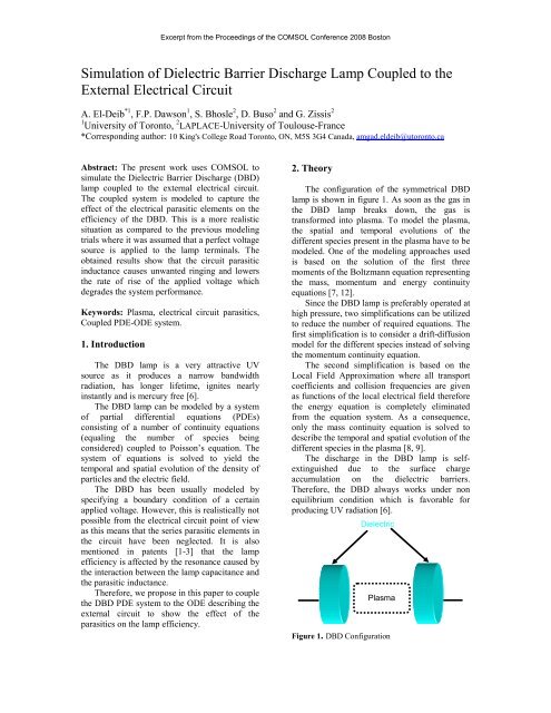
The efficiency <strong>of</strong> the DBD lamp is given as a<br />
function <strong>of</strong> the parasitic inductance in figure 4.<br />
Clearly, as the parasitic inductance increases, the<br />
efficiency <strong>of</strong> the lamp decreases.<br />
V<br />
x 104<br />
1.5<br />
1<br />
0.5<br />
0<br />
-0.5<br />
Ls=1e-5 H<br />
Ls=5e-5 H<br />
Ls=1e-4 H<br />
Ls=5e-4 H<br />
Vs<br />
0 0.5 1 1.5 2 2.5<br />
x 10 -5<br />
-1<br />
Tim Tim e e (s (s ec)<br />
ec)<br />
Figure 3. DBD Voltage under different parasitic<br />
inductances
Percentage Percentage Efficiency<br />
Efficiency<br />
100<br />
90<br />
80<br />
70<br />
60<br />
50<br />
40<br />
30<br />
20<br />
0 0.1 0.2 0.3 0.4 0.5 0.6 0.7 0.8 0.9 1<br />
x 10 -3<br />
10<br />
Ls<br />
Figure 4. Effect <strong>of</strong> L s on DBD Efficiency<br />
6. Discussion<br />
As shown in figure 4, the efficiency <strong>of</strong> the<br />
DBD drops from 92% to about 20% if the<br />
external circuit inductance is increased from zero<br />
to 1mH. Usually the DBD power supply circuit<br />
includes a step up transformer. Since the<br />
transformer leakage inductance that appears on<br />
the lamp side is proportional to the turns ratio<br />
squared, the inductance cannot be neglected in<br />
simulating the DBD lamp performance.<br />
The rate <strong>of</strong> rise <strong>of</strong> VDBD as shown in figure 3<br />
decreases as the inductance value is increased. It<br />
is mentioned in [4, 5] that the voltage rate <strong>of</strong> rise<br />
is one <strong>of</strong> the main factors affecting the optical<br />
efficiency <strong>of</strong> the DBD lamp. The fast rise-time <strong>of</strong><br />
the leading edge <strong>of</strong> the applied voltage heats<br />
electrons simultaneously throughout the entire<br />
active volume, allowing the breakdown to occur<br />
in a diffuse form which is favorable condition for<br />
UV production [11].<br />
Another effect <strong>of</strong> the inductance is the<br />
ringing that takes place after the discharge. This<br />
ringing results only in power deposition in the<br />
plasma without producing UV radiation;<br />
therefore the efficiency is also reduced. This has<br />
been also experimentally verified in [1-3].<br />
7. Conclusions<br />
A PDE system describing the DBD lamp<br />
coupled to an external electric circuit has been<br />
solved using <strong>COMSOL</strong>. Modeling the coupled<br />
system shows the effect <strong>of</strong> the parasitic<br />
inductance on the DBD performance.<br />
Modeling the coupled system is also<br />
beneficial to the power supply designer as this<br />
provides better insight for determining the<br />
required ratings for the devices that are used in<br />
the power supply.<br />
8. References<br />
1. Masashi Okamoto and Kenichi Hirose, “Light<br />
source using dielectric barrier discharge lamp”,<br />
US patent no. 6239559, (2001).<br />
2. Masashi Okamoto and Kenichi Hirose,<br />
“<strong>Dielectric</strong> barrier discharge lamp light source”,<br />
US patent no. 6369519, (2002)<br />
3. Takahiro Hiraoka and Masashi Okamoto,<br />
“Device for operating a dielectric barrier<br />
discharge lamp”, US patent no. 6788088, (2004)<br />
4. Yoshihisa Yokokawa, Masaki Yoshioka and<br />
Takafumi Mizojiri, “Device for operation <strong>of</strong> a<br />
discharge lamp”, US patent no. 6084360, (2000)<br />
5. H. Akashi, A. Oda, Y. Sakai, “Modeling <strong>of</strong><br />
glow like discharge in DBD Xe excimer lamp”,<br />
11 th International Symposium on the Science and<br />
Technology <strong>of</strong> Light Sources, Shanghai, China,<br />
20 th -24 th May 2007<br />
6. U. Kogelschatz, <strong>Dielectric</strong>-barrier <strong>Discharge</strong>s:<br />
Their History, <strong>Discharge</strong> Physics, and Industrial<br />
Applications, Plasma Chemistry and Plasma<br />
Processing, 23 No.1, 1-46 (2003)<br />
7. J. A. Bittencourt, Fundamentals <strong>of</strong> Plasma<br />
Physics, Springer-Verlag, New York (2004)<br />
8. G. E. Georghiou, A. P. Papadais, R. Morrow<br />
and A. C. Metaxas, “Numerical modeling <strong>of</strong><br />
atmospheric pressure gas discharges leading to<br />
plasma production,” J. Phys. D: Appl. Phys., 38,<br />
R303-R328(2005)<br />
9. B. Eliasson and U. Kogelschatz, Modeling and<br />
Applications <strong>of</strong> Silent <strong>Discharge</strong> Plasmas, IEEE<br />
Transactions on Plasma Science, 19 No. 2, 309-<br />
323 (1991)<br />
10. S. Bhosle, G. Zissis, J.J. Damelincourt, A.<br />
Capdevila, "A new approach for boundary<br />
conditions in dielectric barrier discharge<br />
modeling", XVI International Conference on<br />
Gas <strong>Discharge</strong>s and their Applications -<br />
September-11-15, 2006, Xian (China)<br />
11. R. Mildren and R. Carman, Enhanced<br />
performance <strong>of</strong> a dielectric barrier discharge<br />
lamp using short-pulsed excitation, J. Phys. D:<br />
Appl. Phys., 34, L1-L6 (2004)<br />
12. A. Oda, Y. Sakai, H. Akashi, H. Sugawara,<br />
One-dimensional modeling <strong>of</strong> low frequency and<br />
high-pressure Xe barrier discharges for the<br />
design <strong>of</strong> excimer lamps, J. Phys. D: Appl.<br />
Phys., 32, 2726-2736 (1999)
13. "The Siglo Database", CPAT and Kinema<br />
S<strong>of</strong>tware, 1995.<br />
10. Appendix A<br />
A simplified model <strong>of</strong> the Xenon atom, with<br />
only three excited states is considered in this<br />
work. The metastable state 3 P2 <strong>of</strong> Xenon is<br />
named Xe met<br />
*<br />
, the resonant state 3 P1 is Xe res<br />
*<br />
and all the other excited states are gathered and<br />
designated by Xe exc<br />
* . Figure A.1 presents the<br />
chemical model adopted in the simulations.<br />
All the reaction rates <strong>com</strong>e from [12].<br />
Collision frequencies and direct ionization<br />
coefficient αidir have been calculated using the<br />
s<strong>of</strong>tware package Bolsig [13]. The step<br />
ionization coefficient Kipal is taken from [10].<br />
The direct and step ionization coefficients are<br />
shown in figures A.2 and A.3 respectively as<br />
functions <strong>of</strong> E/P where E is the electric field and<br />
P is the pressure <strong>of</strong> the Xenon gas.<br />
The source term Sj in the continuity equation<br />
is formulated from the chemical reactions as the<br />
product <strong>of</strong> the different species densities<br />
involved in the reaction multiplied by the rate<br />
coefficient which represents the probability or<br />
the rate <strong>of</strong> this reaction.<br />
The electron mobility and diffusion<br />
coefficient are obtained from the s<strong>of</strong>tware<br />
program Bolsig [13], whereas the ion diffusion<br />
coefficients and drift velocities are taken from<br />
[12] using a linear interpolation.<br />
Figure A.4 shows the electron mobility and<br />
diffusion coefficient as a function <strong>of</strong> the local<br />
electric field. The diffusion coefficient and the<br />
drift velocity <strong>of</strong> the ions are plotted in figure A.5<br />
as functions <strong>of</strong> the reduced electric field E/N. N<br />
is the density <strong>of</strong> the neutral Xenon atom.<br />
Figure A.1. Chemical model adopted for the modeling<br />
10 2<br />
10 0<br />
10 -2<br />
10 -4<br />
10 -6<br />
10 -8<br />
10 -10<br />
10 -12<br />
10<br />
0 50 100 150 200 250 300<br />
-14<br />
10 -13<br />
10 -14<br />
α idir /P (m -1 .Pa -1 )<br />
E/P (V.m -1 .Pa -1 )<br />
Figure A.2. Direct Ionization Coefficient<br />
10<br />
0 50 100 150 200 250 300<br />
-15<br />
E/P (V.m -1 .Pa -1 )<br />
K ipal (m 3 .s -1 )<br />
Figure A.3. Step Ionization Coefficient<br />
x 104<br />
14<br />
12<br />
10<br />
8<br />
6<br />
4<br />
2<br />
0<br />
0 500 1000 1500 2000 2500 3000<br />
E/P (V.m -1 .Pa -1 )<br />
D e .P (Pa.m 2 .s -1 )<br />
µ e .Px50 (Pa.m 2 .V -1 .s -1 )<br />
Figure A.4. Electron Transport Coefficients
1400<br />
1200<br />
1000<br />
800<br />
600<br />
400<br />
200<br />
D i (Xe + )x2.10 4 (m 2 .s -1 )<br />
D (Xe<br />
+<br />
)x2.10<br />
4<br />
(m<br />
2<br />
.s<br />
-1<br />
)<br />
i 2<br />
µ i .E(Xe + ) (m.s -1 )<br />
+ -1<br />
µ .E(Xe ) (m.s )<br />
i 2<br />
0<br />
0 0.1 0.2 0.3 0.4 0.5 0.6 0.7 0.8 0.9 1<br />
E/N (V.m 2 )<br />
Figure A.5. Ion Transport Coefficients<br />
x 10 -18<br />
The K coefficients used in the flux boundary<br />
conditions for the electrons and ions have the<br />
following the values:<br />
Ksads<br />
Ksdes<br />
Ksrec<br />
10 20<br />
10 10<br />
100<br />
A list <strong>of</strong> the variables included in this work<br />
with the symbol used in the Comsol model is<br />
given in table 1.<br />
Table 1: List <strong>of</strong> Variables<br />
Variable Name Symbol<br />
Voltage PotentielM10<br />
Electron Density ElectronM10<br />
Ion Density IonXeM10<br />
Molecular Ion Density IonXe2M10<br />
Xe met<br />
*<br />
XeMetM10<br />
XeResM10<br />
Xe res<br />
*<br />
Xe exc<br />
* XeExcM10<br />
Excimer (1Σ+u) Exci1SM10<br />
Excimer (3Σ+u) Exci3SM10<br />
Excimer (O+u) ExciOuM10<br />
Electron Surface Density ElectronSurfM10<br />
Ion Surface Density ChargePosSurfM10<br />
i_DBD DBD input current<br />
V_DBD DBD voltage


