

IR2184(4)(S) & (PbF) HALF-BRIDGE DRIVER
IR2184(4)(S) & (PbF) HALF-BRIDGE DRIVER
IR2184(4)(S) & (PbF) HALF-BRIDGE DRIVER

Create successful ePaper yourself
Turn your PDF publications into a flip-book with our unique Google optimized e-Paper software.
Features<br />
• Floating channel designed for bootstrap operation<br />
Fully operational to +600V<br />
Tolerant to negative transient voltage<br />
dV/dt immune<br />
• Gate drive supply range from 10 to 20V<br />
• Undervoltage lockout for both channels<br />
• 3.3V and 5V input logic compatible<br />
• Matched propagation delay for both channels<br />
• Logic and power ground +/- 5V offset.<br />
• Lower di/dt gate driver for better noise immunity<br />
• Output source/sink current capability 1.4A/1.8A<br />
• Also available LEAD-FREE (<strong>PbF</strong>)<br />
Description<br />
The <strong>IR2184</strong>(4)(S) are high voltage,<br />
high speed power MOSFET and IGBT<br />
drivers with dependent high and low<br />
side referenced output channels. Proprietary<br />
HVIC and latch immune<br />
CMOS technologies enable ruggedized<br />
monolithic construction. The<br />
logic input is compatible with standard<br />
CMOS or LSTTL output, down to 3.3V<br />
logic. The output drivers feature a<br />
Typical Connection<br />
<br />
<br />
<br />
<br />
<br />
<br />
<br />
<br />
<br />
<br />
<br />
<strong>IR2184</strong><br />
(Refer to Lead Assignments for correct<br />
configuration). This/These diagram(s) show<br />
electrical connections only. Please refer to<br />
our Application Notes and DesignTips for<br />
proper circuit board layout.<br />
<br />
<br />
<br />
<br />
<br />
<br />
<br />
<br />
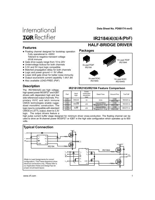
Packages<br />
Data Sheet No. PD60174 revG<br />
<strong>IR2184</strong>(4)(S) & (<strong>PbF</strong>)<br />
<strong>HALF</strong>-<strong>BRIDGE</strong> <strong>DRIVER</strong><br />
<strong>IR2184</strong>4<br />
www.irf.com 1<br />
<br />
<br />
<br />
<br />
<br />
<br />
8-Lead PDIP<br />
<strong>IR2184</strong><br />
<br />
<br />
<br />
<br />
<br />
<br />
<br />
8-Lead SOIC<br />
<strong>IR2184</strong>S<br />
14-Lead PDIP<br />
<strong>IR2184</strong>4<br />
14-Lead SOIC<br />
<strong>IR2184</strong>4S<br />
IR2181/IR2183/<strong>IR2184</strong> Feature Comparison<br />
<br />
<br />
<br />
<br />
<br />
<br />
<br />
<br />
<br />
<br />
<br />
<br />
<br />
<br />
<br />
<br />
<br />
<br />
<br />
<br />
high pulse current buffer stage designed for minimum driver cross-conduction. The floating channel can be<br />
used to drive an N-channel power MOSFET or IGBT in the high side configuration which operates up to 600<br />
volts.
<strong>IR2184</strong>(4)(S) & (<strong>PbF</strong>)<br />
Absolute Maximum Ratings<br />
Absolute maximum ratings indicate sustained limits beyond which damage to the device may occur. All voltage parameters<br />
are absolute voltages referenced to COM. The thermal resistance and power dissipation ratings are measured under board<br />
mounted and still air conditions.<br />
Symbol Definition Min. Max. Units<br />
VB High side floating absolute voltage -0.3 625<br />
VS High side floating supply offset voltage VB - 25 VB + 0.3<br />
VHO High side floating output voltage VS - 0.3 VB + 0.3<br />
VCC<br />
VLO<br />
Low side and logic fixed supply voltage<br />
Low side output voltage<br />
-0.3<br />
-0.3<br />
25<br />
VCC + 0.3<br />
V<br />
DT Programmable dead-time pin voltage (<strong>IR2184</strong>4 only) VSS - 0.3 VCC + 0.3<br />
VIN Logic input voltage (IN & SD) VSS - 0.3 VSS + 10<br />
VSS Logic ground (<strong>IR2184</strong>4 only) VCC - 25 VCC + 0.3<br />
dVS/dt Allowable offset supply voltage transient — 50 V/ns<br />
PD Package power dissipation @ TA ≤ +25°C (8-lead PDIP) — 1.0<br />
(8-lead SOIC) — 0.625<br />
(14-lead PDIP) — 1.6<br />
W<br />
(14-lead SOIC) — 1.0<br />
RthJA Thermal resistance, junction to ambient (8-lead PDIP) — 125<br />
(8-lead SOIC) — 200<br />
(14-lead PDIP) — 75<br />
°C/W<br />
(14-lead SOIC) — 120<br />
TJ Junction temperature — 150<br />
TS Storage temperature -50 150 °C<br />
TL Lead temperature (soldering, 10 seconds) — 300<br />
Recommended Operating Conditions<br />
The input/output logic timing diagram is shown in figure 1. For proper operation the device should be used within the<br />
recommended conditions. The VS and VSS offset rating are tested with all supplies biased at 15V differential.<br />
Symbol Definition Min. Max. Units<br />
VB High side floating supply absolute voltage VS + 10 VS + 20<br />
VS High side floating supply offset voltage Note 1 600<br />
VHO High side floating output voltage VS VB<br />
VCC Low side and logic fixed supply voltage 10 20<br />
VLO Low side output voltage 0 VCC<br />
VIN Logic input voltage (IN & SD) VSS VSS + 5<br />
DT Programmable dead-time pin voltage (<strong>IR2184</strong>4 only) VSS VCC<br />
VSS Logic ground (<strong>IR2184</strong>4 only) -5 5<br />
TA Ambient temperature -40 125 °C<br />
Note 1: Logic operational for VS of -5 to +600V. Logic state held for VS of -5V to -VBS. (Please refer to the Design Tip<br />
DT97-3 for more details).<br />
Note 2: IN and SD are internally clamped with a 5.2V zener diode.<br />
2 www.irf.com<br />
V
<strong>IR2184</strong>(4)(S) & (<strong>PbF</strong>)<br />
Dynamic Electrical Characteristics<br />
VBIAS (VCC, VBS) = 15V, V SS = COM, CL = 1000 pF, TA = 25°C, DT = VSS unless otherwise specified.<br />
Symbol Definition Min. Typ. Max. Units Test Conditions<br />
ton Turn-on propagation delay — 680 900 VS = 0V<br />
toff Turn-off propagation delay — 270 400 VS = 0V or 600V<br />
tsd Shut-down propagation delay — 180 270<br />
MTon Delay matching, HS & LS turn-on — 0 90<br />
MToff Delay matching, HS & LS turn-off — 0 40<br />
tr Turn-on rise time — 40 60 VS = 0V<br />
tf Turn-off fall time — 20 35 VS = 0V<br />
DT Deadtime: LO turn-off to HO turn-on(DTLO-HO) & 280 400 520 RDT= 0<br />
HO turn-off to LO turn-on (DTHO-LO) 4 5 6 µsec RDT = 200k<br />
MDT Deadtime matching = DTLO - HO - DTHO-LO —<br />
—<br />
0<br />
0<br />
50<br />
600<br />
nsec<br />
RDT=0<br />
RDT = 200k<br />
Static Electrical Characteristics<br />
VBIAS (VCC, VBS) = 15V, VSS = COM, DT= VSS and TA = 25°C unless otherwise specified. The VIL, VIH and IIN<br />
parameters are referenced to VSS /COM and are applicable to the respective input leads: IN and SD. The VO, IO and Ron<br />
parameters are referenced to COM and are applicable to the respective output leads: HO and LO.<br />
Symbol Definition Min. Typ. Max. Units Test Conditions<br />
VIH Logic “1” input voltage for HO & logic “0” for LO 2.7 — — VCC = 10V to 20V<br />
VIL Logic “0” input voltage for HO & logic “1” for LO — — 0.8 VCC = 10V to 20V<br />
VSD,TH+<br />
VSD,TH-<br />
SD input positive going threshold<br />
SD input negative going threshold<br />
2.7<br />
—<br />
—<br />
—<br />
—<br />
0.8<br />
V<br />
VCC = 10V to 20V<br />
VCC = 10V to 20V<br />
VOH High level output voltage, VBIAS - VO — — 1.2 IO = 0A<br />
VOL Low level output voltage, VO — — 0.1 IO = 0A<br />
ILK<br />
IQBS<br />
Offset supply leakage current<br />
Quiescent VBS supply current<br />
—<br />
20<br />
—<br />
60<br />
50<br />
150<br />
µA<br />
VB = VS = 600V<br />
VIN = 0V or 5V<br />
IQCC Quiescent VCC supply current 0.4 1.0 1.6 mA VIN = 0V or 5V<br />
IIN+<br />
IIN-<br />
Logic “1” input bias current<br />
Logic “0” input bias current<br />
—<br />
—<br />
25<br />
—<br />
60<br />
1.0<br />
µA<br />
IN = 5V, SD = 0V<br />
IN = 0V, SD = 5V<br />
VCCUV+ VCC and VBS supply undervoltage positive going 8.0 8.9 9.8<br />
VBSUV+ threshold<br />
VCCUV- VCC and VBS supply undervoltage negative going 7.4 8.2 9.0<br />
VBSUV-<br />
VCCUVH<br />
threshold<br />
Hysteresis 0.3 0.7 —<br />
V<br />
VBSUVH<br />
IO+ Output high short circuit pulsed current 1.4 1.9 — VO = 0V,<br />
PW ≤ 10 µs<br />
IO- Output low short circuit pulsed current 1.8 2.3 —<br />
A<br />
VO = 15V,<br />
PW ≤ 10 µs<br />
www.irf.com 3<br />
nsec
<strong>IR2184</strong>(4)(S) & (<strong>PbF</strong>)<br />
4 www.irf.com<br />
Functional Block Diagrams<br />
2184<br />
SD<br />
UV<br />
DETECT<br />
DELAY<br />
IN VS<br />
HO<br />
VB<br />
PULSE<br />
FILTER<br />
HV<br />
LEVEL<br />
SHIFTER<br />
R<br />
R<br />
S<br />
Q<br />
UV<br />
DETECT<br />
PULSE<br />
GENERATOR<br />
VSS/COM<br />
LEVEL<br />
SHIFT<br />
VSS/COM<br />
LEVEL<br />
SHIFT<br />
+5V<br />
DEADTIME<br />
COM<br />
LO<br />
VCC<br />
21844<br />
SD<br />
UV<br />
DETECT<br />
DELAY<br />
IN<br />
DT<br />
VSS<br />
VS<br />
HO<br />
VB<br />
PULSE<br />
FILTER<br />
HV<br />
LEVEL<br />
SHIFTER<br />
R<br />
R<br />
S<br />
Q<br />
UV<br />
DETECT<br />
PULSE<br />
GENERATOR<br />
VSS/COM<br />
LEVEL<br />
SHIFT<br />
VSS/COM<br />
LEVEL<br />
SHIFT<br />
+5V<br />
DEADTIME<br />
COM<br />
LO<br />
VCC
Lead Definitions<br />
Symbol Description<br />
Lead Assignments<br />
8-Lead PDIP 8-Lead SOIC<br />
14-Lead PDIP 14-Lead SOIC<br />
<strong>IR2184</strong>4 <strong>IR2184</strong>4S<br />
<strong>IR2184</strong>(4)(S) & (<strong>PbF</strong>)<br />
IN Logic input for high and low side gate driver outputs (HO and LO), in phase with HO (referenced to COM<br />
for <strong>IR2184</strong> and VSS for <strong>IR2184</strong>4)<br />
SD Logic input for shutdown (referenced to COM for <strong>IR2184</strong> and VSS for <strong>IR2184</strong>4)<br />
DT Programmable dead-time lead, referenced to VSS. (<strong>IR2184</strong>4 only)<br />
VSS Logic Ground (21844 only)<br />
VB High side floating supply<br />
HO High side gate drive output<br />
VS High side floating supply return<br />
VCC Low side and logic fixed supply<br />
LO Low side gate drive output<br />
COM Low side return<br />
1<br />
2<br />
3<br />
4<br />
1<br />
2<br />
3<br />
4<br />
5<br />
6<br />
7<br />
IN<br />
SD<br />
COM<br />
LO<br />
IN<br />
SD<br />
VSS<br />
DT<br />
COM<br />
LO<br />
V CC<br />
VB HO<br />
V S<br />
V CC<br />
8<br />
7<br />
6<br />
5<br />
<strong>IR2184</strong> <strong>IR2184</strong>S<br />
VB HO<br />
V S<br />
14<br />
13<br />
12<br />
11<br />
10<br />
9<br />
8<br />
www.irf.com 5<br />
1<br />
2<br />
3<br />
4<br />
5<br />
6<br />
7<br />
1<br />
2<br />
3<br />
4<br />
IN<br />
SD<br />
COM<br />
LO<br />
IN<br />
SD<br />
VSS<br />
DT<br />
COM<br />
LO<br />
V CC<br />
VB HO<br />
V S<br />
V CC<br />
VB HO<br />
V S<br />
8<br />
7<br />
6<br />
5<br />
14<br />
13<br />
12<br />
11<br />
10<br />
9<br />
8
<strong>IR2184</strong>(4)(S) & (<strong>PbF</strong>)<br />
<br />
<br />
<br />
<br />
Figure 1. Input/Output Timing Diagram Figure 2. Switching Time Waveform Definitions<br />
<br />
<br />
<br />
<br />
<br />
<br />
<br />
<br />
<br />
<br />
<br />
<br />
<br />
Figure 3. Shutdown Waveform Definitions<br />
<br />
<br />
Figure 5. Delay Matching Waveform Definitions<br />
<br />
<br />
<br />
<br />
6 www.irf.com<br />
<br />
<br />
<br />
<br />
<br />
<br />
<br />
<br />
<br />
<br />
<br />
<br />
<br />
<br />
<br />
<br />
<br />
<br />
<br />
<br />
Figure 4. Deadtime Waveform Definitions
Turn-on Propagation Delay (ns)<br />
Turn-off Propagation Delay (ns)<br />
1400<br />
1200<br />
1000<br />
800<br />
600<br />
Max.<br />
Typ.<br />
400<br />
-50 -25 0 25 50 75 100 125<br />
Temperature ( oC) 700<br />
600<br />
500<br />
400<br />
300<br />
200<br />
Figure 4A. Turn-on Propagation Delay<br />
vs. Temperature<br />
Max.<br />
Typ.<br />
100<br />
-50 -25 0 25 50 75 100 125<br />
Temperature ( oC) Figure 5A. Turn-off Propagation Delay<br />
vs. Temperature<br />
<strong>IR2184</strong>(4)(S) & (<strong>PbF</strong>)<br />
www.irf.com 7<br />
Turn-on Propagation Delay (ns)<br />
Turn-off Propagation Delay (ns)<br />
1400<br />
1200<br />
1000<br />
800<br />
600<br />
400<br />
700<br />
600<br />
500<br />
400<br />
300<br />
200<br />
100<br />
Max.<br />
Typ.<br />
10 12 14 16 18 20<br />
Supply Voltage (V)<br />
Max.<br />
Typ.<br />
Figure4B. Turn-on Propagation Delay<br />
vs. Supply Voltage<br />
10 12 14 16 18 20<br />
Supply Voltage (V)<br />
Figure 5B. Turn-off Propagation Delay<br />
vs. Supply Voltage
<strong>IR2184</strong>(4)(S) & (<strong>PbF</strong>)<br />
SD Propagation Delay (ns)<br />
Turn-on Rise Time (ns)<br />
500<br />
400<br />
300<br />
200<br />
100<br />
120<br />
100<br />
80<br />
60<br />
40<br />
20<br />
Max.<br />
Typ.<br />
0<br />
-50 -25 0 25 50 75 100 125<br />
Temperature ( oC) Max.<br />
Typ.<br />
Figure 6A. SD Propagation Delay<br />
vs. Temperature<br />
0<br />
-50 -25 0 25 50 75 100 125<br />
Temperature ( oC) Figure 7A. Turn-on Rise Time vs. Temperature<br />
0<br />
10 12 14 16 18 20<br />
Supply Voltage (V)<br />
8 www.irf.com<br />
SD Propagation Delay (ns)<br />
Turn-on Rise Time (ns)<br />
500<br />
400<br />
300<br />
200<br />
100<br />
120<br />
100<br />
80<br />
60<br />
40<br />
20<br />
0<br />
Max.<br />
Typ.<br />
Max.<br />
Typ.<br />
Figure 6B. SD Propagation Delay<br />
vs. Supply Voltage<br />
10 12 14 16 18 20<br />
Supply Voltage (V)<br />
Figure 7B. Turn-on Rise Time vs. Supply Voltage
Turn-off Fall Time (ns)<br />
Deadtime (ns)<br />
80<br />
60<br />
40<br />
20<br />
0<br />
Max.<br />
Typ<br />
-50 -25 0 25 50 75 100 125<br />
Temperature ( oC) Figure 8A. Turn-off Fall Time vs. Temperature<br />
1100<br />
900<br />
700<br />
500<br />
300<br />
Max.<br />
Typ.<br />
Min.<br />
100<br />
-50 -25 0 25 50 75 100 125<br />
Temperature ( oC) Figure 9A. Deadtime vs. Temperature<br />
<strong>IR2184</strong>(4)(S) & (<strong>PbF</strong>)<br />
0<br />
10 12 14 16 18 20<br />
Supply Voltage (V)<br />
www.irf.com 9<br />
Turn-off Fall Time (ns)<br />
Deaduime (ns)<br />
80<br />
60<br />
40<br />
20<br />
Max.<br />
Typ.<br />
Figure 8B. Turn-off Fall Time vs. Supply Voltage<br />
1100<br />
900<br />
700<br />
500<br />
300<br />
100<br />
Max.<br />
Typ.<br />
Min.<br />
10 12 14 16 18 20<br />
Supply Voltage (v)<br />
Figure 9B. Deadtime vs. Supply Voltage
<strong>IR2184</strong>(4)(S) & (<strong>PbF</strong>)<br />
Deadtime ( Ηs)<br />
Logic "1" Input Voltage (V)<br />
6<br />
5<br />
4<br />
3<br />
2<br />
1<br />
7<br />
6<br />
5<br />
4<br />
3<br />
2<br />
1<br />
0<br />
0 50 100<br />
RDT (KΗ)<br />
150 200<br />
Min.<br />
Figure 9C. Deadtime vs. R DT<br />
Max.<br />
Typ.<br />
Min.<br />
0<br />
10 12 14 16 18 20<br />
Supply Voltage (V)<br />
Figure 10B. Logic "1" Input Voltage<br />
vs. Supply Voltage<br />
0<br />
-50 -25 0 25 50 75 100 125<br />
Temperature ( oC) 10 www.irf.com<br />
Logic "1" Input Voltage (V)<br />
Logic "0" Input Voltage (V)<br />
6<br />
5<br />
4<br />
3<br />
2<br />
1<br />
6<br />
5<br />
4<br />
3<br />
2<br />
1<br />
0<br />
Min.<br />
Max.<br />
Figure 10A. Logic "1" Input Voltage<br />
vs. Temperature<br />
-50 -25 0 25 50 75 100 125<br />
Temperature ( oC) Figure 11A. Logic "0" Input Voltage<br />
vs. Temperature
Logic "0" Input Voltage (V)<br />
SD Input Positive Going Threshold (V)<br />
6<br />
5<br />
4<br />
3<br />
2<br />
1<br />
Max.<br />
0<br />
10 12 14 16 18 20<br />
Supply Voltage (V)<br />
6<br />
5<br />
4<br />
3<br />
2<br />
1<br />
0<br />
Min.<br />
Figure 11B. Logic "0" Input Voltage<br />
vs. Supply Voltage<br />
10 12 14 16 18 20<br />
Supply Voltage (V)<br />
Figure 12B. SD Input Positive Going Threshold<br />
vs. Supply Voltage<br />
<strong>IR2184</strong>(4)(S) & (<strong>PbF</strong>)<br />
www.irf.com 11<br />
SD Input Positive Going Threshold (V)<br />
SD Input Negative Going Threshold (V)<br />
6<br />
5<br />
4<br />
3<br />
2<br />
1<br />
0<br />
Min.<br />
-50 -25 0 25 50 75 100 125<br />
Temperature ( oC) Figure 12A. SD Input Positive Going Threshold<br />
vs. Temperature<br />
5<br />
4<br />
3<br />
2<br />
1<br />
0<br />
Max.<br />
-50 -25 0 25 50 75 100 125<br />
Temperature ( oC) Figure 13A. SD Input Negative Going Threshold<br />
vs. Temperature
<strong>IR2184</strong>(4)(S) & (<strong>PbF</strong>)<br />
SD Input Negative Going Threshold (V)<br />
High Level Output (V)<br />
5<br />
4<br />
3<br />
2<br />
1<br />
Max.<br />
0<br />
10 12 14 16 18 20<br />
Supply Voltage (V)<br />
Figure 13B. SD Input Negative Going Threshold<br />
vs. Supply Voltage<br />
5<br />
4<br />
3<br />
2<br />
1<br />
0<br />
Max.<br />
10 12 14 16 18 20<br />
Supply Voltage (V)<br />
Figure 14B. High Level Output vs. Supply Voltage<br />
0<br />
-50 -25 0 25 50 75 100 125<br />
Temperature ( oC) 12 www.irf.com<br />
High Level Output (V)<br />
Low Level Output (V)<br />
5<br />
4<br />
3<br />
2<br />
1<br />
Max.<br />
Figure 14A. High Level Output vs. Temperature<br />
0.5<br />
0.4<br />
0.3<br />
0.2<br />
0.1<br />
Max.<br />
0.0<br />
-50 -25 0 25 50 75 100 125<br />
Temperature ( oC) Figure 15A. Low Level Output vs. Temperature
Low Level Output (V)<br />
Offset Supply Leakage Current ( ΗA)<br />
0.5<br />
0.4<br />
0.3<br />
0.2<br />
0.1<br />
0.0<br />
Max.<br />
10 12 14 16 18 20<br />
Supply Voltage (V)<br />
Figure 15B. Low Level Output vs. Supply Voltage<br />
500<br />
400<br />
300<br />
200<br />
100<br />
0<br />
Max.<br />
100 200 300 400 500 600<br />
V Boost Voltage (V)<br />
B<br />
Figure 16B. Offset Supply Leakage Current vs.<br />
V B Boost Voltage<br />
<strong>IR2184</strong>(4)(S) & (<strong>PbF</strong>)<br />
0<br />
-50 -25 0 25 50 75 100 125<br />
Temperature ( oC) www.irf.com 13<br />
Offset Supply Leakage Current ( ΗA)<br />
V BS Supply Current ( ΗA)<br />
500<br />
400<br />
300<br />
200<br />
100<br />
Max.<br />
Figure 16A. Offset Supply Leakage Current vs.<br />
Temperature<br />
250<br />
200<br />
150<br />
100<br />
50<br />
Min.<br />
0<br />
-50 -25 0 25 50 75 100 125<br />
Temperature ( oC) Figure 17A. V BS Supply Current<br />
vs. Temperature<br />
Max.<br />
Typ.
<strong>IR2184</strong>(4)(S) & (<strong>PbF</strong>)<br />
V BS Supply Current ( ΗA)<br />
V CC Supply Current (mA)<br />
250<br />
200<br />
150<br />
100<br />
5<br />
4<br />
3<br />
2<br />
1<br />
0<br />
50<br />
0<br />
10 12 14 16 18 20<br />
VBS Floating Supply Voltage (V)<br />
Figure 17B. V BS Supply Current<br />
vs. V BS Floating Supply Voltage<br />
Max.<br />
Typ.<br />
Min.<br />
10 12 14 16 18 20<br />
VCC Supply Voltage (V)<br />
Figure 18B. V CC Supply Current<br />
vs. V CC Supply Voltage<br />
Max.<br />
Typ.<br />
Min.<br />
0<br />
-50 -25 0 25 50 75 100 125<br />
Temperature ( oC) 14 www.irf.com<br />
V CC Supply Current (mA)<br />
Logic "1" Input Bias Current ( ΗA)<br />
5<br />
4<br />
3<br />
2<br />
1<br />
120<br />
100<br />
80<br />
60<br />
40<br />
20<br />
0<br />
Max.<br />
Typ.<br />
Min.<br />
Figure 18A. V CC Supply Current<br />
vs. Temperature<br />
Max.<br />
Typ.<br />
-50 -25 0 25 50 75 100 125<br />
Temperature ( oC) Figure 19A. Logic "1" Input Bias Current<br />
vs. Temperature
Logic "1" Input Bias Current ( ΗA)<br />
Logic "0" Input Bias Current ( ΗA)<br />
120<br />
100<br />
80<br />
60<br />
40<br />
20<br />
5<br />
4<br />
3<br />
2<br />
1<br />
0<br />
Max.<br />
Typ.<br />
10 12 14 16 18 20<br />
Supply Voltage (V)<br />
Max.<br />
Figure 19B. Logic "1" Input Bias Current<br />
vs. Supply Voltage<br />
0<br />
10 12 14 16 18 20<br />
Supply Voltage (V)<br />
Figure 20B. Logic "0" Input Bias Current<br />
vs. Supply Voltage<br />
<strong>IR2184</strong>(4)(S) & (<strong>PbF</strong>)<br />
www.irf.com 15<br />
Logic "0" Input Bias Current ( ΗA)<br />
V CC and V BS UV Threshold (+) (V)<br />
5<br />
4<br />
3<br />
2<br />
1<br />
0<br />
12<br />
11<br />
10<br />
Max.<br />
-50 -25 0 25 50 75 100 125<br />
Temperature ( oC) 9<br />
8<br />
7<br />
6<br />
Max.<br />
Typ.<br />
Min.<br />
Figure 20A. Logic "0" Input Bias Current<br />
vs. Temperature<br />
-50 -25 0 25 50 75 100 125<br />
Temperature ( oC) Figure 21. V CC and V BS Undervoltage Threshold (+)<br />
vs. Temperature
<strong>IR2184</strong>(4)(S) & (<strong>PbF</strong>)<br />
V CC and V BS UVThreshold (-) (V)<br />
Output Source Current (A)<br />
5<br />
4<br />
3<br />
2<br />
1<br />
0<br />
12<br />
11<br />
10<br />
9<br />
8<br />
7<br />
6<br />
Max.<br />
Typ.<br />
Min.<br />
-50 -25 0 25 50 75 100 125<br />
Temperature ( oC) Figure 22. V CC and V BS Undervoltage Threshold (-)<br />
vs. Temperature<br />
Typ.<br />
Min.<br />
10 12 14 16 18 20<br />
Supply Voltage (V)<br />
Figure 23B. Output Source Current<br />
vs. Supply Voltage<br />
16 www.irf.com<br />
Output Source Current (A)<br />
Output Sink Current (A)<br />
5<br />
4<br />
3<br />
2<br />
1<br />
0<br />
Typ.<br />
Min.<br />
-50 -25 0 25 50 75 100 125<br />
Temperature ( oC) 5.0<br />
4.0<br />
3.0<br />
2.0<br />
1.0<br />
Typ.<br />
Min.<br />
Figure 23A. Output Source Current<br />
vs. Temperature<br />
-50 -25 0 25 50 75 100 125<br />
Temperature ( oC) Figure 24A. Output Sink Current<br />
vs. Temperature
Output Sink Current (A)<br />
Temperature ( o C)<br />
5<br />
4<br />
3<br />
2<br />
1<br />
Typ.<br />
Min.<br />
0<br />
10 12 14 16 18 20<br />
Supply Voltage (V)<br />
140<br />
120<br />
100<br />
80<br />
60<br />
40<br />
Figure 24B. Output Sink Current<br />
vs. Supply Voltage<br />
20<br />
1 10 100 1000<br />
Frequency (KHz)<br />
Figure 22. IR2181 vs. Frequency (IRFBC30),<br />
R gate =22Ω, V CC =15V<br />
140v<br />
70v<br />
0v<br />
<strong>IR2184</strong>(4)(S) & (<strong>PbF</strong>)<br />
20<br />
1 10 100 1000<br />
Frequency (KHz)<br />
www.irf.com 17<br />
Temprature ( o C)<br />
Temperature ( o C)<br />
140<br />
120<br />
100<br />
80<br />
60<br />
40<br />
140<br />
120<br />
100<br />
80<br />
60<br />
40<br />
140v<br />
Figure 21. IR2181 vs . Frequency (IRFBC 20),<br />
R gate =33Ω, V CC =15V<br />
20<br />
1 10 100 1000<br />
Frequency (KHz)<br />
Figure 23. IR2181 vs. Frequency (IRFBC40),<br />
R gate =15Ω, V CC =15V<br />
70v<br />
0v<br />
140v<br />
70v<br />
0v
<strong>IR2184</strong>(4)(S) & (<strong>PbF</strong>)<br />
Temperature ( o C)<br />
Temperature ( o C)<br />
140<br />
120<br />
100<br />
80<br />
60<br />
40<br />
20<br />
1 10 100 1000<br />
Frequency (KHz)<br />
Figure 24. IR2181 vs . Frequency (IRFPE50),<br />
R gate =10Ω, V CC =15V<br />
140<br />
120<br />
100<br />
80<br />
60<br />
40<br />
20<br />
1 10 100 1000<br />
Frequency (KHz)<br />
Figure 26. IR21814 vs . Frequency (IRFBC30),<br />
R gate =22Ω, V CC =15V<br />
140v<br />
70v<br />
0v<br />
140v<br />
70v<br />
0v<br />
20<br />
1 10 100 1000<br />
Frequency (KHz)<br />
18 www.irf.com<br />
Temperature ( o C)<br />
Temperature ( o C)<br />
140<br />
120<br />
100<br />
80<br />
60<br />
40<br />
Figure 25. IR21814 vs. Frequency (IRFBC20),<br />
R gate =33Ω, V CC =15V<br />
140<br />
120<br />
100<br />
80<br />
60<br />
40<br />
20<br />
1 10 100 1000<br />
Frequency (KHz)<br />
Figure 27. IR21814 vs. Frequency (IRFBC 40),<br />
R =15Ω, V =15V<br />
gate CC<br />
140v<br />
70v<br />
0v<br />
140v<br />
70v<br />
0v
Temperature ( o C)<br />
Temperature ( o C)<br />
140<br />
120<br />
100<br />
80<br />
60<br />
40<br />
140v<br />
20<br />
1 10 100 1000<br />
Frequency (KHz)<br />
Figure 28. IR21814 vs. Frequency (IRFPE50),<br />
R gate =10Ω, V CC =15V<br />
140<br />
120<br />
100<br />
80<br />
60<br />
40<br />
20<br />
1 10 100 1000<br />
Frequency (KHz)<br />
Figure 30. IR2181s vs. Frequency (IRFBC30),<br />
R gate =22Ω, V CC =15V<br />
70v<br />
0v<br />
140v<br />
70v<br />
0v<br />
<strong>IR2184</strong>(4)(S) & (<strong>PbF</strong>)<br />
20<br />
1 10 100 1000<br />
Frequency (KHz)<br />
www.irf.com 19<br />
Temperature ( o C)<br />
Temperature ( o C)<br />
140<br />
120<br />
100<br />
80<br />
60<br />
40<br />
Figure 29. IR2181s vs . Frequency (IRFBC 20),<br />
R gate =33Ω, V CC =15V<br />
140<br />
120<br />
100<br />
80<br />
60<br />
40<br />
20<br />
1 10 100 1000<br />
Frequency (KHz)<br />
140v<br />
70v<br />
0v<br />
0v<br />
140v 70v<br />
Figure 31. IR2181s vs. Frequency (IRFBC40),<br />
R gate =15Ω, V CC =15V
<strong>IR2184</strong>(4)(S) & (<strong>PbF</strong>)<br />
Tempreture ( o C)<br />
Temperature ( o C)<br />
140<br />
120<br />
100<br />
80<br />
60<br />
40<br />
140V 70V 0V<br />
20<br />
1 10 100 1000<br />
Frequency (KHz)<br />
Figure 32. IR2181s vs. Frequency (IRFPE50),<br />
R gate =10Ω, V CC =15V<br />
140<br />
120<br />
100<br />
80<br />
60<br />
40<br />
20<br />
1 10 100 1000<br />
Frequency (KHz)<br />
Figure 34. IR21814s vs. Frequency (IRFBC30),<br />
R gate =22Ω, V CC =15V<br />
140v<br />
70v<br />
0v<br />
20<br />
1 10 100 1000<br />
Frequency (KHz)<br />
20 www.irf.com<br />
Temperature ( o C)<br />
Temperature ( o C)<br />
140<br />
120<br />
100<br />
80<br />
60<br />
40<br />
Figure 33. IR21814s vs. Frequency (IRFBC20),<br />
R gate =33Ω , V CC =15V<br />
140<br />
120<br />
100<br />
80<br />
60<br />
40<br />
20<br />
1 10 100 1000<br />
Frequency (KHz)<br />
Figure 35. IR21814s vs. Frequency (IRFBC40),<br />
R gate =15Ω, V CC =15V<br />
140v<br />
70v<br />
0v<br />
140v<br />
70v<br />
0v
Temperature ( o C)<br />
140<br />
120<br />
100<br />
80<br />
60<br />
40<br />
20<br />
1 10 100 1000<br />
Frequency (KHz)<br />
<strong>IR2184</strong>(4)(S) & (<strong>PbF</strong>)<br />
140v 70v<br />
Figure 36. IR21814s vs. Frequency (IRFPE50),<br />
R gate =10Ω, V CC =15V<br />
www.irf.com 21<br />
0v
<strong>IR2184</strong>(4)(S) & (<strong>PbF</strong>)<br />
A<br />
E<br />
6<br />
6X<br />
8 7<br />
1 2<br />
e<br />
D B<br />
5<br />
8X b<br />
6 5<br />
3<br />
4<br />
e1<br />
A1<br />
0.25 [.010] C A B<br />
H<br />
0.25 [.010] A<br />
NOTES:<br />
1. DIMENSIONING & TOLERANCING PER ASME Y14.5M-1994.<br />
2. CONTROLLING DIMENSION: MILLIMETER<br />
3. DIMENSIONS ARE SHOWN IN MILLIMETERS [INCHES].<br />
4. OUTLINE CONFORMS TO JEDEC OUTLINE MS-012AA.<br />
A<br />
C<br />
0.10 [.004]<br />
8-Lead PDIP<br />
6.46 [.255]<br />
3X 1.27 [.050]<br />
y<br />
8-Lead SOIC<br />
FOOTPRINT<br />
01-6014<br />
01-3003 01 (MS-001AB)<br />
7 DIMENSION IS THE LENGTH OF LEAD FOR SOLDERING TO<br />
A SUBSTRATE.<br />
01-6027<br />
01-0021 11 (MS-012AA)<br />
22 www.irf.com<br />
8X L<br />
7<br />
8X 0.72 [.028]<br />
K x 45°<br />
8X 1.78 [.070]<br />
8X c<br />
DIM<br />
A .0532<br />
A1 .0040<br />
D<br />
E<br />
e1 .025 BASIC 0.635 BASIC<br />
5 DIMENSION DOES NOT INCLUDE MOLD PROTRUSIONS.<br />
MOLD PROTRUSIONS NOT TO EXCEED 0.15 [.006].<br />
6 DIMENSION DOES NOT INCLUDE MOLD PROTRUSIONS.<br />
MOLD PROTRUSIONS NOT TO EXCEED 0.25 [.010].<br />
b<br />
H<br />
K<br />
L<br />
y<br />
.013<br />
.189<br />
.1497<br />
.050 BASIC<br />
.2284<br />
.0099<br />
.016<br />
0°<br />
INC HES<br />
MIN MAX<br />
.0688<br />
.0098<br />
.020<br />
.1968<br />
.1574<br />
.2440<br />
.0196<br />
.050<br />
8°<br />
MILLIMETERS<br />
MIN MAX<br />
1.35<br />
0.10<br />
0.33<br />
4.80<br />
3.80<br />
1.27 BASIC<br />
5.80<br />
0.25<br />
0.40<br />
0°<br />
1.75<br />
0.25<br />
0.51<br />
c .0075 .0098 0.19 0.25<br />
e<br />
5.00<br />
4.00<br />
6.20<br />
0.50<br />
1.27<br />
8°
14-Lead PDIP<br />
14-Lead SOIC (narrow body)<br />
<strong>IR2184</strong>(4)(S) & (<strong>PbF</strong>)<br />
01-6010<br />
01-3002 03 (MS-001AC)<br />
01-6019<br />
01-3063 00 (MS-012AB)<br />
www.irf.com 23
<strong>IR2184</strong>(4)(S) & (<strong>PbF</strong>)<br />
LEADFREE PART MARKING INFORMATION<br />
Part number<br />
Date code<br />
Pin 1<br />
Identifier<br />
? MARKING CODE<br />
P<br />
IRxxxxxx<br />
YWW?<br />
Lead Free Released<br />
Non-Lead Free<br />
Released<br />
Basic Part (Non-Lead Free)<br />
8-Lead PDIP <strong>IR2184</strong> order <strong>IR2184</strong><br />
8-Lead SOIC <strong>IR2184</strong>S order <strong>IR2184</strong>S<br />
14-Lead PDIP <strong>IR2184</strong>4 order <strong>IR2184</strong>4<br />
14-Lead SOIC <strong>IR2184</strong>4 order <strong>IR2184</strong>4S<br />
?XXXX<br />
ORDER INFORMATION<br />
IR logo<br />
Lot Code<br />
(Prod mode - 4 digit SPN code)<br />
Assembly site code<br />
Per SCOP 200-002<br />
Leadfree Part<br />
8-Lead PDIP <strong>IR2184</strong> order <strong>IR2184</strong><strong>PbF</strong><br />
8-Lead SOIC <strong>IR2184</strong>S order <strong>IR2184</strong>S<strong>PbF</strong><br />
14-Lead PDIP <strong>IR2184</strong>4 order <strong>IR2184</strong>4<strong>PbF</strong><br />
14-Lead SOIC <strong>IR2184</strong>4 order <strong>IR2184</strong>4S<strong>PbF</strong><br />
Thisproduct has been designed and qualified for the industrial market.<br />
Qualification Standards can be found on IR’s Web Site http://www.irf.com<br />
Data and specifications subject to change without notice.<br />
IR WORLD HEADQUARTERS: 233 Kansas St., El Segundo, California 90245 Tel: (310) 252-7105<br />
4/4/2006<br />
24 www.irf.com


