Programm Photovoltaik Ausgabe 2009 ... - Bundesamt für Energie BFE
Programm Photovoltaik Ausgabe 2009 ... - Bundesamt für Energie BFE Programm Photovoltaik Ausgabe 2009 ... - Bundesamt für Energie BFE
3/5 Tasks of the collaboration partners New materials (Ciba, TUE): Ciba’s competence in synthesizing tailor-made materials for a variety of dye applications is crucial for this project. The challenge in the design of synthetic organic semiconductors for solar cells is to optimize the absorption spectra (for matching the illumination), the transport energy levels and mobilities (for low electrical losses) as well as the electron-hole binding energy (for efficient dissociation). Solubility and printability concerns add additional constraints. A new series of small band gap donor-type polymers with high intrinsic charge carrier mobility and energy levels that are optimized for charge carrier generation in combination with PCBM need to be synthesized. Of the most promising materials multi-gram quantities will be available for further studies and printing at the other partners. Cell optimization and new concepts (TUE, CSEM): Even though the excited state energy of the absorbing solar cell material can be as high as 2 eV, the open-circuit voltage is typically as low as 0.6V. This represents a loss by a factor of 3 and is one example of the room for improvement. While high efficiencies and innovative concepts were demonstrated with multi-cell stacks at TUE, in this project we will focus on low-complexity cell concepts that are feasible for printing. Solution-processed organic solar cells rely on bulk heterojunctions that must separate the charges effectively. These blends must be optimized for high efficiency, open-circuit voltage and fill factor. Combinatorial device fabrication by use of a high-throughput pipetting robot (cf. figure 3) and automatic characterization has proven highly useful for OLED research and development at CSEM and shall be explored for solar cells. The active layers need to be fully characterized with respect to their morphology and optical absorption. The IQE, EQE, and J-V characteristics of the devices will be characterized to determine the major loss mechanisms and –hence – identify opportunities for further optimization. Figure 2: CSEM’s ink-jet printer (left) and the high throughput fabrication robot (HTF-7) for polymer devices based on a modified pipetting robot (right). Cell characterization methods and tools (UJI, TUE, CSEM, ZHAW): Electrical characterization of solar cells by impedance spectroscopy has been pioneered at UJI for dye sensitized solar cells. Equivalent circuit models are physically motivated and able to reveal loss mechanisms. While impedance spectroscopy has also been employed in the past to study OLEDs, little is known in the context of organic solar cells and the numerical modelling thereof. Cell modelling (ZHAW, UJI): A comprehensive device model for the study of operation mechanisms and the interpretation of measured data will be developed. It will cover the whole process chain from light absorption, exciton dissociation, charge carrier transport and collection by electrodes. The ZHAW has expertise in numerical modelling of opto-electronic processes in transient and steady state in OLEDs. The maximum achievable short circuit-current will be addressed with optical simulations that provide the spatial exciton generation rate density. It is intended to distinguish the detrimental effects of charge trap, recombination and collection losses by the use of drift-diffusion simulations. APOLLO, B. Ruhstaller, ICP ZHAW 137/290
Cell prototyping (CSEM): CSEM has established organic layer deposition by spinning, ink-jetting (cf. figure 3), screen printing as well as hot-embossing of 3D structures as part of an EU-project (“ROLLED”) on roll-to-roll OLED fabrication. The printing challenges arise with viscosity constraints, interface roughness, thickness non-uniformity etc. and lead to a reduction of the record efficiencies compared to spin-coated devices. Performed work and achievements At the kick-off meeting in November 2008 in Winterthur the project partners presented their institutes / companies and the first results in material tailoring and simulation results have been discussed. First simulation results The calculation of optical-electromagnetic-field penetration spectrum can be seen in figure 3 (top). This plot shows the square of the electromagnetic field inside the device. This gives a hint of the actual optical intensity inside the device. This device has an additional spacer layer (ZnO) which does not absorb any light [2,3]. From this calculation the photon absorption profile can be calculated which is shown in figure 4 (bottom). As a next step one can calculate the maximum achievable short circuit current Isc,max by summing up the amount of absorbed photons in the active layer (P3HT:PCBM). The knowledge of this is important to tune the thickness of a device to increase the short circuit current. APOLLO, B. Ruhstaller, ICP ZHAW Figure 3: Optical Field penetration spectrum (top) and calculated photon absorption spectrum (bottom). 138/290 4/5
- Page 90 and 91: Eidgenössisches Departement für U
- Page 92 and 93: 3/7 Work performed and results achi
- Page 94 and 95: 5/7 Fig. 3: Raman spectra recorded
- Page 96: 7/7 Measurements of solar cells per
- Page 99 and 100: Introduction / project objectives T
- Page 101 and 102: Optimum Na dosage Sodium layer with
- Page 103 and 104: application might become more impor
- Page 105 and 106: In a second experiment the amount o
- Page 108 and 109: Eidgenössisches Departement für U
- Page 110 and 111: 3/9 After optimizing the In2S3 buff
- Page 112 and 113: 5/9 Indium sulfide layer characteri
- Page 114 and 115: 7/9 3) Semitransparent CIGS solar c
- Page 116: 9/9 Steps towards multi-junction so
- Page 119 and 120: Introduction / project objectives T
- Page 121 and 122: Figure 2: SEM picture of laser-abla
- Page 123 and 124: Introduction / project objectives T
- Page 125 and 126: Work progress and achievements duri
- Page 127 and 128: Furthermore, with a good reproducib
- Page 129 and 130: Main achievements - The association
- Page 131 and 132: Introduction Dye-sensitized solar c
- Page 134 and 135: Eidgenössisches Departement für U
- Page 136 and 137: 3/4 So far, experiments were perfor
- Page 138 and 139: Eidgenössisches Departement für U
- Page 142: 5/5 Figure 4: Maximum achievable sh
- Page 145 and 146: Project Goals The goal is the estab
- Page 147 and 148: Evaluation 2008 and Outlook 2009 L'
- Page 149 and 150: Project Goals NAPOLYDE industrials
- Page 151 and 152: � Organic large solar panel and
- Page 153 and 154: Materials such as the conductive ca
- Page 155 and 156: National and international collabor
- Page 157 and 158: Project Goals The aim of FULLSPECTR
- Page 159 and 160: In addition, every two years, the P
- Page 161 and 162: The table below show the change of
- Page 163 and 164: The table below shows the change of
- Page 165 and 166: 4. The UV-A tests with PMMA films c
- Page 167 and 168: Introduction / Project Goals The co
- Page 169 and 170: Fig. 4. Schematic illustration of a
- Page 172 and 173: THINPV Eidgenössisches Departement
- Page 174 and 175: 3/6 IR laser source Pumping line IR
- Page 176 and 177: 5/6 Figure 2: Scheme of a monolithi
- Page 178 and 179: PECNET Eidgenössisches Departement
- Page 180 and 181: 3/10 Projektziele Dieses Forschungs
- Page 182 and 183: 5/10 und mit Stichworten katalogisi
- Page 184 and 185: 7/10 einer Vorverpflichtung mit rel
- Page 186 and 187: 9/10 NanoPEC Partner IEA HIA Annex
- Page 188: Module und Gebäudeintegration T. S
3/5<br />
Tasks of the collaboration partners<br />
New materials (Ciba, TUE): Ciba’s competence in synthesizing tailor-made materials for a variety of<br />
dye applications is crucial for this project. The challenge in the design of synthetic organic semiconductors<br />
for solar cells is to optimize the absorption spectra (for matching the illumination), the transport<br />
energy levels and mobilities (for low electrical losses) as well as the electron-hole binding energy (for<br />
efficient dissociation). Solubility and printability concerns add additional constraints.<br />
A new series of small band gap donor-type polymers with high intrinsic charge carrier mobility and energy<br />
levels that are optimized for charge carrier generation in combination with PCBM need to be synthesized.<br />
Of the most promising materials multi-gram quantities will be available for further studies and<br />
printing at the other partners.<br />
Cell optimization and new concepts (TUE, CSEM): Even though the excited state energy of the<br />
absorbing solar cell material can be as high as 2 eV, the open-circuit voltage is typically as low as<br />
0.6V. This represents a loss by a factor of 3 and is one example of the room for improvement. While<br />
high efficiencies and innovative concepts were demonstrated with multi-cell stacks at TUE, in this project<br />
we will focus on low-complexity cell concepts that are feasible for printing. Solution-processed organic<br />
solar cells rely on bulk heterojunctions that must separate the charges effectively. These blends<br />
must be optimized for high efficiency, open-circuit voltage and fill factor. Combinatorial device fabrication<br />
by use of a high-throughput pipetting robot (cf. figure 3) and automatic characterization has<br />
proven highly useful for OLED research and development at CSEM and shall be explored for solar<br />
cells.<br />
The active layers need to be fully characterized with respect to their morphology and optical absorption.<br />
The IQE, EQE, and J-V characteristics of the devices will be characterized to determine the major<br />
loss mechanisms and –hence – identify opportunities for further optimization.<br />
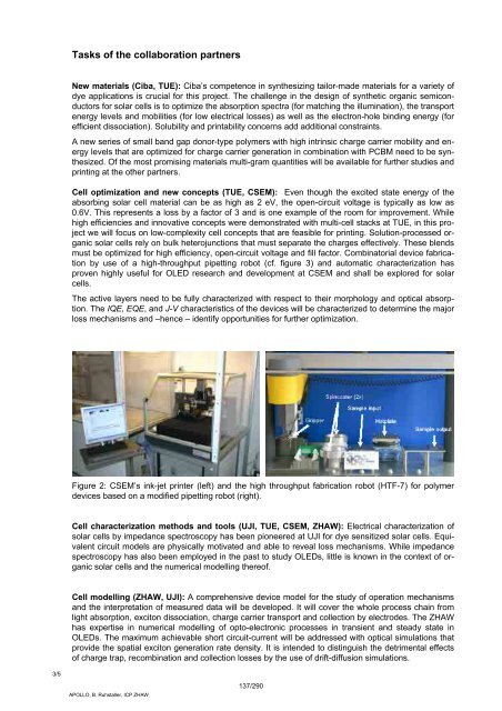
Figure 2: CSEM’s ink-jet printer (left) and the high throughput fabrication robot (HTF-7) for polymer<br />
devices based on a modified pipetting robot (right).<br />
Cell characterization methods and tools (UJI, TUE, CSEM, ZHAW): Electrical characterization of<br />
solar cells by impedance spectroscopy has been pioneered at UJI for dye sensitized solar cells. Equivalent<br />
circuit models are physically motivated and able to reveal loss mechanisms. While impedance<br />
spectroscopy has also been employed in the past to study OLEDs, little is known in the context of organic<br />
solar cells and the numerical modelling thereof.<br />
Cell modelling (ZHAW, UJI): A comprehensive device model for the study of operation mechanisms<br />
and the interpretation of measured data will be developed. It will cover the whole process chain from<br />
light absorption, exciton dissociation, charge carrier transport and collection by electrodes. The ZHAW<br />
has expertise in numerical modelling of opto-electronic processes in transient and steady state in<br />
OLEDs. The maximum achievable short circuit-current will be addressed with optical simulations that<br />
provide the spatial exciton generation rate density. It is intended to distinguish the detrimental effects<br />
of charge trap, recombination and collection losses by the use of drift-diffusion simulations.<br />
APOLLO, B. Ruhstaller, ICP ZHAW<br />
137/290


