Programm Photovoltaik Ausgabe 2008 ... - Bundesamt für Energie BFE
Programm Photovoltaik Ausgabe 2008 ... - Bundesamt für Energie BFE
Programm Photovoltaik Ausgabe 2008 ... - Bundesamt für Energie BFE

Create successful ePaper yourself
Turn your PDF publications into a flip-book with our unique Google optimized e-Paper software.
Seite 56 von 288<br />
Introduction / Project goals<br />
This project focuses on the most promising material and device options for thin film technologies,<br />
namely cadmium-free cells and modules, based on amorphous, micro- and polycrystalline silicon as<br />
well as on chalcopyrite compound semiconductors (CIGS). Research is organized either along the<br />
value chain of each technology or with a trans-disciplinary (or trans-technology) character in order to<br />
target every aspect of the module development from the substrate to the encapsulated module.<br />
The overall goal is to provide the scientific and technological basis for an industrial mass production of<br />
cost effective and highly efficient, environmentally sound, large-area thin film solar cells and modules.<br />
By drawing on a broad basis of expertise, the entire range of module fabrication and supporting R&D<br />
is covered: Substrates, semiconductor and contact deposition, monolithic series interconnection, encapsulation,<br />
performance evaluation and applications.<br />
The main objectives are:<br />
� significantly reducing the cost/efficiency ratio: towards 0.5 €/Wp on the long run<br />
� providing the know-how and the scientific basis for large-area PV modules by identifying and testing<br />
new materials and technologies with maximum cost reduction<br />
� developing the process know-how and the production technology as well as the design and fabrication<br />
of specialised equipment resulting in low costs and high yield in the production of large<br />
area thin film modules.<br />
In the case of thin-film silicon solar cells, the specific objectives are the following:<br />
� The development of large area micromorph modules (> 1 m 2 ) with a 10% stable efficiency deposited<br />
at �10 Å/s<br />
� A production concept for module cost < 0.5 €/Wp<br />
Development of high efficiency thin-film Si cell on small area is also part of the project with a target<br />
stable efficiency of 14%.<br />
Description of the project<br />
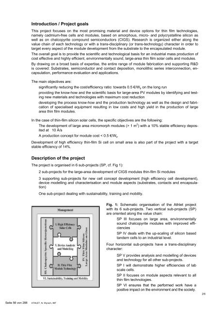
The project is organised in 6 sub-projects (SP, cf. Fig 1):<br />
� 2 sub-projects for the large-area development of CIGS modules thin-film Si modules<br />
� 3 supporting sub-projects for new cell concept development (high efficiency cell development),<br />
device modelling and characterisation and module aspects (substrates, contacts and encapsulation)<br />
� One sub-project dealing with sustainability, training and mobility.<br />
ATHLET, N. Wyrsch, IMT<br />
Fig. 1: Schematic organisation of the Athlet project<br />
with its 6 sub-projects. Two vertical sub-projects (SP)<br />
are oriented along the value chain:<br />
� SP III focuses on large area, environmentally<br />
sound chalcopyrite modules with improved efficiencies<br />
� SP IV deals with the up-scaling of silicon based<br />
tandem cells to an industrial level.<br />
Four horizontal sub-projects have a trans-disciplinary<br />
character:<br />
� SP V provides analysis and modelling of devices<br />
and technology for all other sub-projects.<br />
� SP I will demonstrate higher efficiencies of lab<br />
scale cells.<br />
� SP II focuses on module aspects relevant to all<br />
thin film technologies.<br />
� SP VI ensures that the performed work have a<br />
positive impact on the environment and the society.<br />
2/6