Programm Photovoltaik Ausgabe 2008 ... - Bundesamt für Energie BFE
Programm Photovoltaik Ausgabe 2008 ... - Bundesamt für Energie BFE
Programm Photovoltaik Ausgabe 2008 ... - Bundesamt für Energie BFE

You also want an ePaper? Increase the reach of your titles
YUMPU automatically turns print PDFs into web optimized ePapers that Google loves.
3/7<br />
Results<br />
Substrates<br />
The goal is to fabricate high quality , cost-effective substrates by roll-to-roll processing with a focus on:<br />
� Metal foils with insulating layers, light-trapping, nanotexture, high quality reflector,<br />
� Plastic webs (PET/PEN) with light-trapping, nanotextures, high-quality reflector,<br />
Sprayed SiOx based insulating layers are developed by ECN. High breakdown voltages up to 900V on<br />
A4 metal foils (4*4mm 2 contacts) are achieved. The sprayed layers fabrication is compatible with rollto-roll<br />
and suitable for embossing, as shown by Fig.2. Textured PEN and PET plastic substrates fabricated<br />
by roll-to-roll at OVD-Kinegram are coated at FEP with various high quality Ag/ZnO or Al/ZnO<br />
stacks. Reliable back-reflector on plastic are achieved on which short-circuit Jsc gains up to 20% are<br />
measured in a-Si:H and µc-Si:H cells (see section 3.3).<br />
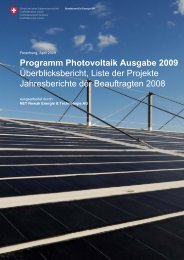
Fig. 2: Insulating layer textured by hot embossing before curing (embossing performed at UBA)<br />
Deposition processes<br />
The focus is set on the development and comparison of three different deposition techniques for the<br />
intrinsic a-Si:H and �c-Si:H layers: MW-PECVD, HWCVD and VHF-PECVD. Besides achieving device<br />
quality layers, high deposition rates are targeted for intrinsic µc-Si:H. At that stage of the project, a<br />
“fair” assessment of the deposition techniques in terms of �c-Si.H deposition rates and cost effectiveness<br />
is still not possible, as the VHF process is at a far more advanced stage of development.<br />
i) Deposition by MW-PECVD<br />
A new pilot roll-to-roll system built by R&R in partnership with ECN was installed and ramped-up at<br />
ECN. The doped layers are obtained by using RF-linear sources (see [2, 3]), whereas the i- layer are<br />
deposited by MW-PECVD. The roll-to-roll system is fully operational, and several doped layers are now<br />
of satisfying quality [3]. The development of device quality intrinsic a-Si and µc-Si layers is underway.<br />
ii) Deposition by HW-CVD<br />
At the moment, the new chamber, designed and taken into operation by the University of Barcelona, is<br />
being used to perform HWCVD deposition of cells and layers in static mode. Currently, a roll-to-roll<br />
charger is being designed and will be installed in the system. More details are given in [4].<br />
iii) Deposition by VHF-PECVD<br />
VHF-PECVD deposition is performed in batch static process at UniNe and in the pilot roll-to-roll line at<br />
VHF.<br />
As shown in section 3.3, VHF deposition allows high quality devices fabrication on PEN plastic substrates.<br />
µc-Si:H intrinsic layers have been deposited successfully on PEN foil in the roll-to-roll system<br />
at VHF.<br />
Besides, intrinsic µc-Si:H layer deposition at 2nm/s are obtained in batch deposition but low compatibility<br />
with plastic substrates such as PEN is observed, associated in large part to substrate overheating.<br />
A deposition regime at 0.8nm/s in a new low-flow low-power regime compatible with low cost plastic<br />
substrates allows the fabrication of device quality layers.<br />
Flexcellence, C. Ballif, IMT Seite 49 von 288