Programm Photovoltaik Ausgabe 2008 ... - Bundesamt für Energie BFE
Programm Photovoltaik Ausgabe 2008 ... - Bundesamt für Energie BFE
Programm Photovoltaik Ausgabe 2008 ... - Bundesamt für Energie BFE

You also want an ePaper? Increase the reach of your titles
YUMPU automatically turns print PDFs into web optimized ePapers that Google loves.
Seite 36 von 288<br />
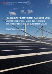
Fig. 7: View of the new fully automated cluster system at IMT. One chamber is operational whereas<br />
the second plasma box is being installed at the time of writing this report.<br />
Collaboration and synergies with other projects/institutes<br />
IMT continues to be involved into the European projects ATHLET and FLEXCELLENCE. A strong<br />
synergy is realized between all these projects and this running SFOE project, with indirect benefits for<br />
companies such as OC Oerlikon and VHF-Technologies. A project (1.3.2006-28.2.<strong>2008</strong>) with the Danish<br />
company “Photosolar” financed by <strong>Energie</strong>net.dk continues to allow synergy for nip devices development.<br />
Regular academic contacts/scientific and sample exchanges have been maintained throughout 2007<br />
both with national (CRPP-EPFL, EMPA, HE-Arc,..) and international (University of Ljubljana, University<br />
of Patras, IPV Juelich, Academy of Science of Prague, ECN….). IMT was one of the instigators of the<br />
Swiss thin Film PV project, coordinated now by EMPA (Sponsored by CCEM-CH and Swiss Eletric<br />
Research). One Phd. student performed measurements at HMI in Berlin. One IMT Phd. student stayed<br />
for six months at NREL (Golden, CO, US) and developed new technique for thin film Si analyses. In<br />
2007, IMT organized two “Thin film PV schools” for industries. These schools last 5-9 days and offer<br />
an in-depth introduction to the science and technology of thin film silicon.<br />
Evaluation for 2007 / perspectives for <strong>2008</strong><br />
2007 has been a fruitful year as it has allowed both the introduction of new concepts in the thin film<br />
silicon devices (e.g. SiOX intermediate reflector) and a much better understanding of the critical interaction<br />
between the substrate morphology and the PECVD thin film growth. This knowledge is now<br />
useful for virtually all thin film silicion devices, prepared both on glass and plastic. In general, we have<br />
now much better tools (receipts, processes, TCO’s, backreflector) in hands to fabricate high efficiency<br />
devices on a variety of different TCO's or substrates, and this with different device concepts. In particular,<br />
micromorph solar cells with initial efficiency above 12% can be routinely prepared and this can<br />
be achieved either with devices with a high Voc and FF or with a high current. The reasons for the<br />
difficulty to achieve simultaneously both high VOC FF and current are now better understood and give<br />
clear guidelines for the next steps.<br />
In the next years, the laboratory will continue the upgrade of its infrastructure with the introduction of<br />
new state-of-the-art multi chamber cluster systems (small area systems, with up to 7 chambers) allowing<br />
the introduction of more innovative layers and processes. In parallel, it will continue its work with<br />
the development of high efficiency devices and development of processes which will be relevant for<br />
the next generation production lines based on thin film silicon.<br />
Thin film silicon solar cells: advanced processing and characterization, C. Ballif, IMT<br />
8/9