- Page 1:
Forschung, April 2008 Programm Phot
- Page 4 and 5:
Programm Photovoltaik Ausgabe 2008
- Page 6 and 7:
T. Meyer ORGAPVNET: Coordination Ac
- Page 8 and 9:
PROGRAMM PHOTOVOLTAIK Eidgenössisc
- Page 10 and 11:
1. Programmschwerpunkte und anvisie
- Page 12 and 13:
Ein neues KTI-Projekt Flexible Phot
- Page 14 and 15:
In einem neuen, durch den Axpo Natu
- Page 16 and 17:
Performanz und Energieproduktion vo
- Page 18 and 19:
ERGÄNZENDE PROJEKTE UND STUDIEN En
- Page 20 and 21:
in diesem Projekt für die Koordina
- Page 22 and 23:
5. Pilot- und Demonstrationsprojekt
- Page 24 and 25:
Produktionskapazität von insgesamt
- Page 26 and 27:
[26] H. Häberlin, L. Borgna, D. Gf
- Page 28 and 29:
[89] Konzept der Energieforschung d
- Page 30 and 31:
Solarzellen C. Ballif, J. Bailat, F
- Page 32 and 33:
Département fédéral de l’envir
- Page 34 and 35:
3/9 Fig. 1: Refractive index n and
- Page 36 and 37:
5/9 V oc [mV] 940 920 900 880 860 8
- Page 38 and 39:
7/9 Fig. 5: Top) SEM micrographs of
- Page 40:
9/9 Acknowledgements The co-workers
- Page 43 and 44:
Seite 40 von 288 Introduction and f
- Page 45 and 46:
Seite 42 von 288 Introduction / Pro
- Page 47 and 48:
Seite 44 von 288 Results The amorph
- Page 49 and 50:
Seite 46 von 288 Collaborations IMT
- Page 51 and 52:
Seite 48 von 288 Introduction / Pro
- Page 53 and 54: Seite 50 von 288 High efficiency so
- Page 55 and 56: Seite 52 von 288 Towards low costs
- Page 58 and 59: Eidgenössisches Departement für U
- Page 60 and 61: 3/6 The Athlet consortium comprises
- Page 62 and 63: 5/6 Large area cluster deposition s
- Page 64 and 65: SIWIS Département fédéral de l
- Page 66 and 67: 3/6 Results Defects characterizatio
- Page 68 and 69: 5/6 The test methodology was optimi
- Page 70: Département fédéral de l’envir
- Page 73 and 74: Seite 70 von 288 Summary of Applied
- Page 75 and 76: Seite 72 von 288 Table 5 summarizes
- Page 78 and 79: Eidgenössisches Departement für U
- Page 80 and 81: 3/7 Figure 1: Vacuum deposition equ
- Page 82 and 83: 5/7 Testing of thickness, chemical
- Page 84: 7/7 Figure 6: Large area flexible s
- Page 87 and 88: Seite 84 von 288 Introduction / Pro
- Page 89 and 90: Seite 86 von 288 Intensity / arb. u
- Page 92 and 93: LARCIS Eidgenössisches Departement
- Page 94 and 95: 3/6 Work and results Alternative Ba
- Page 96 and 97: 5/6 As expected the addition of Na
- Page 98 and 99: ATHLET Eidgenössisches Departement
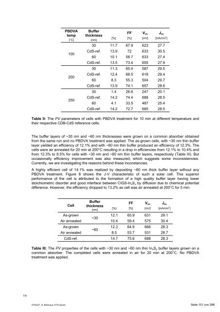
- Page 100 and 101: 3/9 ZnO:Al/ZnO was deposited by rf-
- Page 102 and 103: 5/9 Figure 4: XRD pattern of powder
- Page 106: 9/9 National and international coll
- Page 109 and 110: Introduction / Project Goals Thin f
- Page 111 and 112: Introduction The work to be reporte
- Page 113 and 114: Ongoing Work and Results 2007 Dye d
- Page 115 and 116: International Cooperation Internati
- Page 117 and 118: Introduction Dye-sensitized solar c
- Page 119 and 120: Figure 2: Upper panel: isodensity p
- Page 122 and 123: Eidgenössisches Departement für U
- Page 124: 3/3 (a) (b) I N ClO ClO4- 4- Al ITO
- Page 127 and 128: Seite 124 von 288 Project Goals The
- Page 129 and 130: Seite 126 von 288 Within the activi
- Page 131 and 132: Seite 128 von 288 Typical UV-Vis sp
- Page 133 and 134: Seite 130 von 288 National and inte
- Page 135 and 136: Project Goals The goal is the estab
- Page 138 and 139: NAPOLYDE Département fédéral de
- Page 140 and 141: 3/7 � PECVD/Sputtering Co-deposit
- Page 142 and 143: 5/7 Work and results SP2.4 - Nanola
- Page 144: 7/7 Evaluation 2007 and Outlook 200
- Page 147 and 148: Projektziele In der Schweiz bestehe
- Page 149 and 150: Die wichtigsten erreichten Ziele de
- Page 151 and 152: Energy Center (EC) der EPFL Univers
- Page 153 and 154: Für 2008 ist in Zusammenarbeit mit
- Page 156 and 157:
BIPV-CIS Eidgenössisches Departeme
- Page 158:
3/3 Bewertung 2007 und Ausblick 200
- Page 162 and 163:
Département fédéral de l’envir
- Page 164 and 165:
3/9 Service measurements In 2007 a
- Page 166 and 167:
5/9 Type of meas. Direct with c-Si
- Page 168 and 169:
7/9 c-Si reference cell for the mea
- Page 170:
9/9 � 4 energy rating comparison
- Page 173 and 174:
1. Traceable performance measuremen
- Page 175 and 176:
The following list shows the measur
- Page 177 and 178:
data sets. The indoor data sets con
- Page 179 and 180:
The blind round-robin proved that o
- Page 181 and 182:
Einleitung / Projektziele Herstelle
- Page 183 and 184:
Abb. 1, und deren Mittelwert für d
- Page 185 and 186:
Aus Gleichung (1) ergeben sich der
- Page 187 and 188:
Abb. 7: Abhängigkeit des Wirkungsg
- Page 189 and 190:
Der Rechengang zu Abb.8 läuft wie
- Page 191 and 192:
Wie erwartet ist der Jahresmittelwe
- Page 193 and 194:
Projektziele für 2007 � Ununterb
- Page 195 and 196:
Generator-Korrekturfaktor k G in %
- Page 197 and 198:
WR-Defekte pro WR-Betriebsjahr 0.8
- Page 199 and 200:
Nationale / internationale Zusammen
- Page 201 and 202:
Einleitung / Projektziele Dezentral
- Page 203 and 204:
BON: Betrieb ohne Netz oder USV-Bet
- Page 205 and 206:
An einem Workshop mit EWs in Kalifo
- Page 207 and 208:
Nationale / internationale Zusammen
- Page 209 and 210:
Challenges The liberalisation of th
- Page 211 and 212:
W 900 800 700 600 500 400 300 200 1
- Page 214 and 215:
PV-BUK Eidgenössisches Departement
- Page 216 and 217:
3/6 häufigsten traten jedoch Gesam
- Page 218 and 219:
5/6 Die Gespräche mit verschiedene
- Page 220 and 221:
Eidgenössisches Departement für U
- Page 222 and 223:
3/10 Tab. 1: Overview of the types
- Page 224 and 225:
5/10 Tab. 2: Key parameters of the
- Page 226 and 227:
7/10 horizontal surface (kWh/m 2 )
- Page 228 and 229:
9/10 6. Conclusion and Outlook The
- Page 230 and 231:
Eidgenössisches Departement für U
- Page 232 and 233:
3/9 Fig.2: Photograph of SiO2:CdS s
- Page 234 and 235:
5/9 Fig. 4: Photoluminescence spect
- Page 236 and 237:
7/9 In general, the performance of
- Page 238:
9/9 Conclusions � A large Stokes
- Page 241 and 242:
Einleitung / Projektziele Solaranla
- Page 244:
Internationale Koordination P. Hüs
- Page 247 and 248:
Kurzbeschrieb des Projekts Task 1 u
- Page 249 and 250:
Trends Report Basierend auf den Dat
- Page 251 and 252:
Nationale / internationale Zusammen
- Page 253 and 254:
Einleitung / Projektziele Die Ziele
- Page 255 and 256:
Case Studies Als Ergänzung zu den
- Page 258 and 259:
Eidgenössisches Departement für U
- Page 260 and 261:
3/10 Ziele 2007 Die Ziele der REPIC
- Page 262 and 263:
5/10 Die restlichen 13 Projektantr
- Page 264 and 265:
7/10 Stand der technischen REPIC Pr
- Page 266 and 267:
9/10 Förderung der Solarenergie f
- Page 268 and 269:
Département fédéral de l’envir
- Page 270 and 271:
3/6 Les avantages pour le consommat
- Page 272 and 273:
5/6 SOUS-TÂCHE 4 « Information et
- Page 274 and 275:
Eidgenössisches Departement für U
- Page 276:
3/3 Turbidity climatology Turbidity
- Page 279 and 280:
Einleitung / Projektziele Normenarb
- Page 281 and 282:
IEC 62548 Installation and Safety R
- Page 283 and 284:
Referenzen Eine vollständige Liste
- Page 285 and 286:
Introduction and Goals PV ERA NET i
- Page 287 and 288:
WP2: Strategy Issues: The main acti
- Page 289 and 290:
A dedicated transnational call “P
- Page 291:
Databases have been developed for o