Programm Photovoltaik Ausgabe 2008 ... - Bundesamt für Energie BFE
Programm Photovoltaik Ausgabe 2008 ... - Bundesamt für Energie BFE
Programm Photovoltaik Ausgabe 2008 ... - Bundesamt für Energie BFE

You also want an ePaper? Increase the reach of your titles
YUMPU automatically turns print PDFs into web optimized ePapers that Google loves.
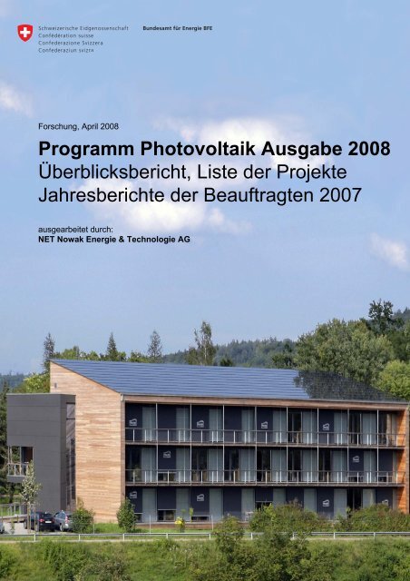
Forschung, April <strong>2008</strong><br />
<strong>Programm</strong> <strong>Photovoltaik</strong> <strong>Ausgabe</strong> <strong>2008</strong><br />
Überblicksbericht, Liste der Projekte<br />
Jahresberichte der Beauftragten 2007<br />
ausgearbeitet durch:<br />
NET Nowak <strong>Energie</strong> & Technologie AG
Titelbild:<br />
Nullenergie Verwaltungsgebäude Marché International, Kemptthal / ZH<br />
44,6 kWp <strong>Photovoltaik</strong>anlage realisiert mit Dünnschicht-Solarzellen<br />
(Bildquellen: Frontseite: SunTechnics Fabrisolar AG, Rückseite: Büro <strong>für</strong> Architektur Beat Kämpfen, Foto Willi Kracher)<br />
ausgearbeitet durch:<br />
NET Nowak <strong>Energie</strong> & Technologie AG<br />
Waldweg 8, CH - 1717 St. Ursen (Schweiz)<br />
Tel. +41 (0) 26 494 00 30, Fax. +41 (0) 26 494 00 34, info@netenergy.ch<br />
im Auftrag des:<br />
<strong>Bundesamt</strong> <strong>für</strong> <strong>Energie</strong> <strong>BFE</strong><br />
Mühlestrasse 4, CH - 3063 Ittigen Postadresse: CH- 3003 Bern<br />
Tel. 031 322 56 11, Fax. 031 323 25 00 office@bfe.admin.ch www.bfe.admin.ch
<strong>Programm</strong> <strong>Photovoltaik</strong> <strong>Ausgabe</strong> <strong>2008</strong><br />
Forschung<br />
Inhalt<br />
S. Nowak<br />
Überblicksbericht des <strong>Programm</strong>leiters Seite 5<br />
Jahresberichte der Beauftragten Seite<br />
Solarzellen<br />
C. Ballif, J. Bailat, F.J. Haug, S. Faÿ, R. Tscharner<br />
Thin film silicon solar cells: advanced processing and characterization -<br />
101191 / 151399<br />
F.J. Haug, C. Ballif<br />
Flexible photovoltaics: next generation high efficiency and low cost thin<br />
film silicon modules - CTI 8809<br />
S. Olibet, C. Ballif<br />
High efficiency thin-film passivated silicon solar cells and modules -<br />
THIFIC: Thin film on crystalline Si - Axpo Naturstrom Fonds 0703<br />
C. Ballif, F. J. Haug, V. Terrazzoni-Daudrix<br />
FLEXCELLENCE: Roll-to-roll technology for the production of high efficiency<br />
low cost thin film silicon photovoltaic modules - SES-CT-019948<br />
N. Wyrsch, C. Ballif<br />
ATHLET: Advanced Thin Film Technologies for Cost Effective Photovoltaics -<br />
IP 019670<br />
29<br />
39<br />
41<br />
47<br />
55<br />
Seite 1 von 288
Seite 2 von 288<br />
A. Bidiville, K. Wasmer, P. M. Nasch, M. Van der Meer, C. Ballif, J. Michler<br />
SIWIS: Ultra Thin Silicon Wafer Cutting by Multi-Wire Sawing -<br />
CTI Nº 7730.2 NMPP-NM<br />
A. Dimitrov, P. Hoffmann, P. Nasch<br />
SIRE: Silicon recycling from wafering waste to produce reusable photovoltaic<br />
feedstock - CTI 8829.2 PFIW-IW<br />
P. Nasch, S. Schneeberger<br />
BITHINK: Bifacial thin industrial multi-crystalline silicon solar cells -<br />
503105 / SBF 03.0086<br />
D. Brémaud, M. Kälin, A. N. Tiwari<br />
Large Area flexible CIGS: Flexible CIGS solar cells on large area polymer foils<br />
with in-line deposition methods and application of alternative back contacts -<br />
100964 / 152404<br />
A. N. Tiwari, M. Kälin<br />
Thin Film CIGS Solar Cells with a Novel Low Cost Process – 100964 / 152223 83<br />
D. Brémaud, A. N. Tiwari<br />
LARCIS: Large-Area CIS Based Thin-Film Solar Modules for Highly Productive<br />
Manufacturing - SES66-CT-2005-019757 / FP6-019757<br />
D. Brémaud, R. Verma, S. Bücheler, S. Seyrling, A. N. Tiwari<br />
ATHLET: Advanced Thin-Film Technologies for Cost Effective Photovoltaics -<br />
ATHLET CIS / FP-2204-Energy-3<br />
M. Kaelin<br />
Development of flexible CIGS Solar Modules with metal Grids -<br />
Axpo Naturstrom Fonds<br />
M. Grätzel, A. Mc Evoy<br />
Dye-sensitised Nanocrystalline Solar Cells - Project EPFL 107<br />
Y.-H. Yum, P.Walter, S. Huber, D. Rentsch, T. Geiger, F. Nüesch,<br />
F. De Angelis, M. Grätzel, M. K. Nazeeruddin<br />
ThinPV - Efficient Far Red sensitization of Nanocrystalline TiO2 films by an<br />
unsymmetrical squaraine dye - CCEM-ThinPV project Part B; Empa<br />
B. Fan, R. Hany, F. Nüesch, J.-E. Moser<br />
ThinPV - Doping of cyanine solar cells: enhancing charge transport -<br />
CCEM-ThinPV project Part B<br />
T. Meyer, A. Meyer<br />
FULLSPECTRUM: A new PV wave making more efficient use of the solar<br />
spectrum - SES6-CT-2003-502620 / SER N° 03.0111-2<br />
61<br />
67<br />
69<br />
75<br />
89<br />
95<br />
105<br />
113<br />
119<br />
123
T. Meyer<br />
ORGAPVNET: Coordination Action towards stable and low-cost organic solar<br />
cell technologies and their application - SES6-038889<br />
T. Meyer, A. Meyer<br />
NAPOLYDE: Nano structured polymer deposition processes for mass production<br />
of innovative systems for energy production & control and for smart devices -<br />
NMP2-CT-2005-515846 / SER N° 03.0111-2<br />
M. Spirig, A. Luzzi<br />
PECNet: Aufbau eines Schweizer Kompetenznetzwerks <strong>für</strong> die Solare<br />
Wasserspaltung mittels hybrider PV-PEC Zellen -101883 / 152316<br />
Module und Gebäudeintegration<br />
T. Szacsvay<br />
BIPV-CIS- Improved integration of PV into existing buildings by using thin<br />
film modules for retrofit – 503777 / SBF 03.0046<br />
Systemtechnik<br />
D. Chianese, A. Bernasconi, N. Cereghetti, A. Realini, G. Friesen, E. Burà,<br />
I. Pola, K. Nagel<br />
Centrale di test ISAAC-TISO: Qualità e resa energetica di moduli fotovoltaici -<br />
36508 / 151135<br />
G. Friesen<br />
PERFORMANCE - ISAAC Activities - n° 019718 EU: (SES6) – Integrated project 169<br />
W. Durisch, J.-C. Mayor, K. Hang Lam<br />
Efficiency and Annual Electricity Production of PV-Modules - 101431 / 151715 177<br />
H. Häberlin, L. Borgna, D. Gfeller, M. Kämpfer, U. Zwahlen<br />
<strong>Photovoltaik</strong> Systemtechnik 2007-2010 / PVSYSTE 07-10 - 102234 / 152840 189<br />
P. Toggweiler, S. Stettler, P. Felder<br />
Solar Inverter mit integriertem BackUp SIMIBU - 101807 / 152227 197<br />
P. Gaillard<br />
SOS-PVI: Security of Supply Photovoltaic Inverter - SUSTDEV-1.2.3 205<br />
131<br />
135<br />
143<br />
153<br />
159<br />
Seite 3 von 288
Seite 4 von 288<br />
Diverse Projekte und Studien<br />
S. Stettler, P. Toggweiler<br />
PV-BUK - Betriebs- und Unterhaltskosten von PV-Anlagen – 102070 / 152575 211<br />
N. Jungbluth, M. Tuchschmid<br />
Update Photovoltaic in view of ecoinvent data v2.0 - 101805 / 152224 217<br />
A. Schüler, A. Kostro, B. Huriet<br />
Evaluation du potentiel de concentrateurs à Quantum Dots pour la production<br />
d'électricité photovoltaïque - 101806 / 152225<br />
R. Durot<br />
Center of competence for building integrated solar installations - 102014 / 152494 237<br />
Internationale Koordination<br />
P. Hüsser<br />
Schweizer Beitrag zum IEA PVPS <strong>Programm</strong> - Task 1 - 11427 / 152 582 243<br />
Th. Nordmann, L. Clavadetscher<br />
IEA PVPS <strong>Programm</strong> Task 2 Schweizer Beitrag 2007 - 14805 / 152583 249<br />
S. Nowak, G. Favaro, M. Gutschner<br />
Swiss Interdepartmental Platform for Renewable Energy Promotion in<br />
International Cooperation (REPIC) - SECO UR-00123.01.01<br />
P. Renaud, P. Bonhôte<br />
IEA PVPS Task 10 – Swiss contribution - 101562 / 151862 265<br />
J. Remund, M. Rindlisbacher, D. Domeisen<br />
IEA SHC Task 36: Solar resource knowledge management - 101498 / 151784 271<br />
M. Real, T. Hostettler<br />
Normenarbeit <strong>für</strong> PV Systeme - Swissolar 275<br />
S. Nowak, M. Gutschner, S. Gnos, U. Wolfer<br />
PV-ERA-NET: Networking and Integration of National and Regional <strong>Programm</strong>es<br />
in the Field of Photovoltaic (PV) Solar Energy Research and Technological<br />
Development (RTD) in the European Research Area (ERA) - CA-011814-<br />
PV ERA NET<br />
227<br />
255<br />
281
PROGRAMM PHOTOVOLTAIK<br />
Eidgenössisches Departement <strong>für</strong><br />
Umwelt, Verkehr, <strong>Energie</strong> und Kommunikation UVEK<br />
<strong>Bundesamt</strong> <strong>für</strong> <strong>Energie</strong> <strong>BFE</strong><br />
Überblicksbericht zum Forschungsprogramm 2007<br />
Stefan Nowak<br />
stefan.nowak@netenergy.ch<br />
<strong>Energie</strong>rücklaufzeit der <strong>Photovoltaik</strong> – eine häufig wiederkehrende Frage:<br />
Im Rahmen der Überarbeitung der Ecoinvent-Datenbank wurde die <strong>Energie</strong>rücklaufzeit der <strong>Photovoltaik</strong><br />
anhand von aktuellen industriellen Prozessen und Produkten ermittelt. Obige Darstellung zeigt die<br />
<strong>Energie</strong>rücklaufzeit einer multikristallinen 3 kWp-Schrägdachanlage in Europa mit dem UCTE-<br />
Elektrizitätsmix als Referenz (Bildquelle: ESU Services).<br />
Seite 5 von 288
Seite 6 von 288<br />
Inhaltsverzeichnis<br />
1. <strong>Programm</strong>schwerpunkte und anvisierte Ziele........................................................................... 7<br />
2. Durchgeführte Arbeiten und erreichte Ergebnisse 2007.......................................................... 8<br />
Zell-Technologie............................................................................................................................. 8<br />
Solarmodule und Gebäudeintegration ......................................................................................... 12<br />
Elektrische Systemtechnik ........................................................................................................... 12<br />
Ergänzende Projekte und Studien ............................................................................................... 15<br />
Internationale Zusammenarbeit IEA, IEC, EU.............................................................................. 16<br />
3. Nationale Zusammenarbeit........................................................................................................ 18<br />
4. Internationale Zusammenarbeit ................................................................................................ 18<br />
5. Pilot- und Demonstrationsprojekte (P+D) ................................................................................ 19<br />
Neue P+D Projekte ...................................................................................................................... 19<br />
Laufende P+D Projekte ................................................................................................................ 19<br />
Im Jahr 2007 abgeschlossene P+D Projekte............................................................................... 20<br />
6. Bewertung 2007 und Ausblick <strong>2008</strong> ......................................................................................... 20<br />
7. Liste der F+E-Projekte................................................................................................................ 22<br />
8. Liste der P+D-Projekte ............................................................................................................... 23<br />
9. Referenzen .................................................................................................................................. 24<br />
10. Für weitere Informationen ......................................................................................................... 25<br />
11. Verwendete Abkürzungen (inkl. Internetlinks)........................................................................ 25<br />
12. Weiterführende Internetlinks..................................................................................................... 26
1. <strong>Programm</strong>schwerpunkte und anvisierte Ziele<br />
Die <strong>Photovoltaik</strong> erfuhr im Jahr 2007 weltweit wie auch in der Schweiz einen weiteren Aufschwung.<br />
Davon war auch das <strong>Programm</strong> <strong>Photovoltaik</strong> massgeblich betroffen, indem immer mehr vor allem<br />
auch industrielle Akteure sich mit der <strong>Photovoltaik</strong> auseinandersetzen, Ideen und Konzepte formulieren<br />
und Projekte entwickeln. Durch die anfangs des Jahres durch das Parlament beschlossene Einführung<br />
der kostendeckenden Vergütung <strong>für</strong> Strom aus erneuerbaren <strong>Energie</strong>n erhielten anwendungsorientierte<br />
Fragestellungen an zusätzlicher Bedeutung. Durch die breite <strong>Programm</strong>abstützung<br />
im Bereich der Forschung konnte das bisherige Niveau gehalten werden. Das anhaltende Wachstum<br />
des internationalen <strong>Photovoltaik</strong> Marktes bildet eine wichtige Grundlage <strong>für</strong> den weiterhin erfolgenden,<br />
deutlichen Ausbau der <strong>Photovoltaik</strong> Industriebasis in der Schweiz.<br />
Das <strong>Programm</strong> <strong>Photovoltaik</strong> verfolgt eine ausgeprägte Ausrichtung auf die industrielle Umsetzung und<br />
die internationale Wettbewerbsfähigkeit, sowohl <strong>für</strong> Produkte wie auch <strong>für</strong> die vorgelagerte Forschung.<br />
Laufende Aktivitäten in Forschung und Entwicklung sowie noch bestehende Projekte im Bereich von<br />
Pilot- und Demonstrationsanlagen umfassen im Berichtsjahr 2007 ca. 55 Projekte, wobei alle bekannten<br />
Projekte mit einer Förderung der öffentlichen Hand berücksichtigt sind.<br />
Gestützt auf das <strong>Energie</strong>forschungskonzept der Eidgenössischen <strong>Energie</strong>forschungskommission<br />
CORE [61] verfolgt das Schweizer <strong>Photovoltaik</strong> <strong>Programm</strong> in der Periode 2004 – 2007 die folgenden<br />
wesentlichen Ziele [62]:<br />
� Es soll eine weitere Kostenreduktion (� Preise) des <strong>Energie</strong>systems <strong>Photovoltaik</strong> erreicht werden<br />
(typische Werte 2007: Modul 2.5 CHF/Wp; System 5 CHF/Wp) und entsprechende Verbesserungen<br />
der einzelnen Komponenten in Bezug auf elektrische Eigenschaften (2007: Dünnschichtmodule<br />
mit >12% Wirkungsgrad), Herstellungskosten und industrielle Fertigung;<br />
� Etablierung bzw. Konsolidierung der industriellen Basis <strong>für</strong> Produkte der <strong>Photovoltaik</strong>, einschliesslich<br />
Solarzellen und Module in ausgewählten Technologieansätzen;<br />
� Hohe Integration und Standardisierung der Produkte und Systeme <strong>für</strong> Massenmärkte.<br />
Dazu ist das <strong>Programm</strong> <strong>Photovoltaik</strong> in folgende Bereiche aufgeteilt:<br />
SOLARZELLEN DER ZUKUNFT<br />
Die Arbeiten zu Dünnschicht Solarzellen waren im Berichtsjahr wie bisher fokussiert auf die<br />
Schwerpunkte Silizium (amorph, mikrokristallin), Zellen auf der Basis von Verbindungshalbleitern<br />
(CIGS) sowie Farbstoffzellen. Neue Konzepte (Materialien und Prozesse), z.B. organische und Polymersolarzellen,<br />
<strong>für</strong> langfristige Technologieoptionen gewinnen in der Grundlagenforschung gesamthaft<br />
an Bedeutung und bewegen sich gleichzeitig vom Konzept zur Solarzelle. Die mit Nachdruck verfolgte<br />
Industrialisierung von Produktionsprozessen steht bei den Silizium Dünnschicht Solarzellen in<br />
einem fortgeschrittenen Stadium, bei den Verbindungshalbleitern ist ein industrielles Projekt im Aufbau.<br />
Im Jahr 2007 wurden erstmals in der Schweiz konkrete grössere Fertigungsanlagen mit Dünnschicht<br />
Solarzellen angekündigt. Solarzellen auf flexiblen Substraten gewinnen zudem weiterhin an<br />
Bedeutung.<br />
MODULE UND GEBÄUDEINTEGRATION<br />
Die Integration der <strong>Photovoltaik</strong> im bebauten Raum bildet weiterhin den wichtigsten Schwerpunkt<br />
der angestrebten Anwendungen. Währenddem der Markt <strong>für</strong> Montagesysteme mittlerweile eine breite<br />
Produktpalette anbieten kann, stellen neue Produkte und Erfahrungen mit Dünnschicht Solarzellen in<br />
der Gebäudeintegration weiterhin ein wachsendes Thema dar.<br />
ELEKTRISCHE SYSTEMTECHNIK<br />
Die Qualitätssicherung von <strong>Photovoltaik</strong>modulen, von Wechselrichtern und von gesamten Systemen<br />
ist, zusammen mit Langzeitbeobachtungen an diesen Komponenten, <strong>für</strong> die Praxis von anhaltender<br />
Bedeutung und wird in entsprechenden Kompetenzzentren an Fachhochschulen bearbeitet. Langjährige<br />
Messreihen und die vermehrte Analyse von Fehlverhalten der einzelnen Komponenten sollen in<br />
Hinsicht auf kritische Parameter und die Erhöhung der Lebensdauer genutzt werden. Aufgrund dieser<br />
systembezogenen Arbeiten soll die spezifische <strong>Energie</strong>produktion von <strong>Photovoltaik</strong>-Anlagen<br />
(kWh/kWp) weiter erhöht werden. Für Inselanlagen wächst die Bedeutung der Kombination mit anderen<br />
<strong>Energie</strong>technologien in Hybridanlagen.<br />
Seite 7 von 288
Seite 8 von 288<br />
ERGÄNZENDE PROJEKTE UND STUDIEN<br />
Die Arbeiten in diesem Bereich sollen die Grundlagen zu allgemeinen Fragestellungen im Zusammenhang<br />
mit dem Marktaufbau der <strong>Photovoltaik</strong> liefern, insbesondere zu Potenzial, Umweltaspekten<br />
und <strong>Energie</strong>planung sowie praxisorientierten Hilfsmitteln zur Anlagenplanung und –überwachung.<br />
Neuste Technologien des Internets, Computermodelle, Bildverarbeitung, geografische Informationssysteme<br />
bis hin zur Satellitenkommunikation gelangen dabei zum Einsatz. Für Anwendungen in Entwicklungsländern<br />
stehen dagegen nicht-technische Aspekte im Vordergrund. Dieser Bereich des<br />
<strong>Programm</strong>s umfasst zudem die Vorhaben an den Schnittstellen zu anderen <strong>Energie</strong>technologien.<br />
INSTITUTIONELLE INTERNATIONALE ZUSAMMENARBEIT<br />
Die internationale Zusammenarbeit bildet ein zentrales Standbein in allen Bereichen. Der Anschluss<br />
an die internationale Entwicklung sowie ein intensivierter Informationsaustausch war im Berichtsjahr<br />
ein wichtiges Ziel, welches im Rahmen der internationalen <strong>Programm</strong>e der EU sowie der IEA mit Kontinuität<br />
weiterverfolgt wurde. Die erfolgreiche internationale Zusammenarbeit konnte in einigen der<br />
grossen EU-Projekte (IP - Integrated Projects – Integrierte Projekte) fortgesetzt werden. Von übergeordneter<br />
Bedeutung war im Berichtsjahr zudem die Schweizer Beteiligung an den Arbeiten in europäischen<br />
Netzwerken (PV-ERA-NET und Europäische <strong>Photovoltaik</strong> Technologie Plattform). Dabei ist<br />
die Publikation der Strategic Research Agenda for Photovoltaic Solar Energy Technology [63] der<br />
Europäische <strong>Photovoltaik</strong> Technologie Plattform besonders hervorzuheben.<br />
2. Durchgeführte Arbeiten und erreichte Ergebnisse 2007<br />
ZELL-TECHNOLOGIE<br />
Die grosse Bandbreite der Schweizer Solarzellenforschung konnte im Berichtsjahr 2007 dank der<br />
breiten Abstützung dieser Forschung mit Erfolg fortgesetzt werden. Die Beteiligung an EU-Projekten<br />
des 6. Rahmenforschungsprogramms sowie KTI-Projekte bildeten hier gewichtige Elemente. Die<br />
Schweiz ist mittlerweile an den meisten laufenden Integrierten Projekten der Europäischen Kommission<br />
im Bereich der <strong>Photovoltaik</strong> direkt oder indirekt beteiligt.<br />
a) Dünnschicht Silizium<br />
Die Entwicklungen im Bereich des Dünnschicht Siliziums finden an der Universität Neuchâtel (IMT), an<br />
der EPFL (CRPP), der Haute Ecole Arc ingénierie (Le Locle), dem NTB (Buchs) sowie bei den Unternehmen<br />
oerlikon solar (Trübbach und Neuchâtel) und VHF-Technologies (Yverdon) statt und stellen<br />
den wichtigsten Schwerpunkt des <strong>Photovoltaik</strong> <strong>Programm</strong>s dar.<br />
Das IMT an der Universität Neuchâtel schloss im Berichtsjahr die aktuelle Phase des Projektes zu<br />
Silizium Dünnschicht Solarzellen [1] ab. Die Ziele dieses <strong>BFE</strong>-Projektes bestanden darin, den Wirkungsgrad<br />
der Solarzellen auf verschiedenen Substraten weiter zu erhöhen (Ziel 14% <strong>für</strong> mikromorphe<br />
Solarzellen), die Prozessführung und Charakterisierung der Solarzellen weiter zu entwickeln und<br />
die notwendige Infrastruktur (Prozesse, Herstellung und Charakterisierung) zur Unterstützung der<br />
Industriepartner sicherzustellen. Dazu wurden verschiedene Depositionssysteme erneuert und automatisiert,<br />
die Systeme zur Charakterisierung der Solarzellen standardisiert und ein spezieller Akzent<br />
auf die Reproduzierbarkeit der einzelnen Fabrikationsschritte gelegt. Die Zusammenarbeit mit der<br />
Industrie erfolgte primär mit den Unternehmen oerlikon solar und VHF-Technologies, welche ihrerseits<br />
die am IMT entwickelten Prozesse in ihre Produkte implementieren. Folgende Resultate wurden im<br />
Berichtsjahr erreicht:<br />
Aufbauend auf den Resultaten der Vorjahre <strong>für</strong> amorphe und mikrokristalline Einfach Solarzellen (single<br />
junction) auf Glassubstraten und der Entwicklung von Zwischenreflektor Schichten wurde eine<br />
weitere Erhöhung des Wirkungsgrads der mikromorphen Solarzelle angestrebt. Nachdem die Zwischenreflektor<br />
Schicht bisher auf ZnO aufgebaut war, wurde im Berichtsjahr dazu intensiv mit SiOx<br />
Schichten gearbeitet. Mit diesem Material wurde im Berichtsjahr <strong>für</strong> mikromorphe Solarzellen vom<br />
1.2 cm 2 Fläche ein Anfangswirkungsgrad von 12.6% erreicht. Auf Kunststoffsubstraten wurden sowohl<br />
amorphe wie mikrokristalline Solarzellen hoher Qualität hergestellt. Mikrokristalline Solarzellen auf<br />
PET (Polyethylenterephthalat) bzw. PEN (Polyethylennaphtalat) erreichten einen Wirkungsgrad von<br />
8.6%. Das physikalische Verständnis der optoelektronischen Eigenschaften von ZnO, insbesondere<br />
der Einfluss der Korngrenzen des Materials auf die Mobilität der Ladungsträger, konnte verbessert<br />
werden. Ein neues, automatisiertes Doppelkammer-Depositionssystem konnte erfolgreich in Betrieb<br />
genommen werden (Fig 1).
Ein neues KTI-Projekt Flexible Photovoltaics – next generation high efficiency and low cost thin<br />
film silicon modules [2] hat im Berichtsjahr zwischen dem IMT der Universität Neuchâtel und VHF-<br />
Technologies begonnen. In diesem Vorhaben wird angestrebt, die bisher bei VHF-Technologies in<br />
ihrer ersten Produktgeneration bei flexiblen Solarzellen realisierten Wirkungsgrade von ca. 4.5% signifikant<br />
zu erhöhen. Durch die Einführung eines rückseitigen, diffus streuenden Reflektors und einer<br />
amorphen Zellenstruktur in Tandemkonfiguration soll der Wirkungsgrad der industriellen Produkte auf<br />
6% erhöht werden. Es wurden auf kleiner Fläche erste vielversprechende Ergebnisse mit einem Wirkungsgrad<br />
von 8.8% erreicht.<br />
In einem neuen, durch den Axpo Naturstrom Fonds unterstützten Projekt THIFIC – Thin film on crystalline<br />
silicon [3] werden am IMT ultra hocheffiziente Solarzellen von 20-22% Wirkungsgrad angestrebt.<br />
Dabei kommt das bekannte Konzept einer Heteroverbindung (hetero junction) zwischen kristallinen<br />
Silizium Solarzellen und amorphen bzw. mikrokristallinen Solarzellen zur Anwendung (HIT-Zelle).<br />
Der Vorteil liegt in der Verwendung von Siliziumwafern deutlich geringerer Dicke bis gegen 100 µm<br />
und entsprechender Material- bzw. <strong>Energie</strong>einsparung. In Vorarbeiten zu diesem Vorhaben wurde<br />
bereits ein Wirkungsgrad von 19% erreicht. Nun geht es darum, mit texturierten Wafern noch bessere<br />
Resultate zu erzielen.<br />
Das IMT und VHF-Technologies arbeiten, zusammen mit weiteren Partnern aus der EU, im EU-<br />
Projekt FLEXCELLENCE [4] am Thema der flexiblen Solarzellen auf Kunststoff- und Metallsubstraten,<br />
wobei die Gesamtkoordination des Projektes durch das IMT erfolgt. Im Berichtsjahr konnten nanotexturierte<br />
Substrate auf Metall- und Plastikfolien hergestellt werden. Im Vorhaben werden drei unterschiedliche<br />
Ansätze zur roll-to-roll Beschichtung untersucht, namentlich Mikrowellen PECVD (Plasma<br />
Enhanced Chemical Vapor Deposition), Hot Wire CVD (Chemical Vapor Deposition) und VHF PECVD.<br />
Das IMT bzw. VHF-Technologies befassen sich mit dem letzten der drei genannten Verfahren. Am<br />
IMT wurde im Berichtsjahr mittels PECVD eine mikromorphe Tandemzelle auf Kunststoff mit einem<br />
Wirkungsgrad von 10.9% realisiert. Auf dieser Grundlage könnten bei einem Wirkungsgrad von 10%<br />
in der industriellen Fertigung tiefe Kosten von < 0.6 €/Wp erzielt werden.<br />
Im Integrierten EU-Projekt ATHLET [5] befassen sich das IMT und oerlikon solar mit der Weiterentwicklung<br />
der Dünnschicht Silizium Solarzellen. Für mikromorphe Tandemzellen lautet das Ziel 10%<br />
stabiler Wirkungsgrad bei einer Fläche von 1 m 2 und 10 Å/s Depositionsrate bzw. Modulproduktionskosten<br />
von < 0.5 €/Wp. Dieses Projekt ergänzt das eingangs aufgeführte <strong>BFE</strong> Projekt am IMT. Im KAI-S<br />
Reaktor konnte im Berichtsjahr ein Anfangswirkungsgrad von 10.5% erzielt werden. oerlikon solar<br />
demonstrierte an der 22. europäischen <strong>Photovoltaik</strong> Konferenz in Mailand erste grossflächige (1.3 x<br />
1.4 m 2 ) mikromorphe Module mit einem Wirkungsgrad von 9.46%.<br />
Figur 1: Automatisiertes Dünnschichtsilizium- Figur 2: MRC Sputteranlage zur Abscheidung<br />
Doppelkammer-Depositionssystem auf der der Front- und Rückkontakte in 30 x 30 cm 2<br />
Grundlage der KAI-M plasma box von oerlikon CIGS Dünnschicht Solarzellen<br />
(Bildquelle: IMT) (Bildquelle: ETHZ)<br />
Seite 9 von 288
Seite 10 von 288<br />
b) Kristallines Silizium<br />
Im KTI-Projekt SIWIS [6] erarbeitet die EMPA Thun in Zusammenarbeit mit Applied Materials Switzerland<br />
(vormals HCT Shaping Systems) die Mechanismen, welche bei Drahtsägen von dünnen Silizium<br />
Waferscheiben zu Oberflächendefekten führen können, um daraus entsprechende Modelle zu entwickeln.<br />
Übergeordnetes Ziel des Vorhabens ist die Herstellung von Wafern unter 100 µm Dicke <strong>für</strong> die<br />
Produktion von kristallinen Siliziumsolarzellen. In Funktion der Sägeparameter konnte eine Korrelation<br />
zwischen der Oberflächenrauheit und der Bildung von Spalten bzw. der mechanischen Festigkeit festgestellt<br />
werden. Trotz Abschluss des Vorhabens als KTI-Projekt soll die Zusammenarbeit fortgesetzt<br />
werden.<br />
In einer neuen KTI-Machbarkeitsstudie SIRE [7] untersucht die Fachhochschule Genf zusammen mit<br />
Applied Materials Switzerland die Möglichkeiten zum Recycling von Silizium aus Sägeabfällen. Es<br />
konnte gezeigt werden, dass das Silizium vom Siliziumkarbid getrennt werden kann.<br />
Das von Applied Materials Switzerland verfolgte EU-Projekt BITHINK [8] wurde im Berichtsjahr abgeschlossen.<br />
Die Waferdicke konnte dabei auf von 280 auf 90 µm reduziert werden. Dies führt zu einer<br />
Anzahl Wafer pro Meter festes Silizium von rund 3500 bzw. 1.45 m 2 Silizium Wafer pro kg Silizium. In einer<br />
bifacialen Solarzelle führt dies bei 13% Wirkungsgrad zu einem Siliziumverbrauch von 3.9 – 4.6 g/Wp.<br />
Kann der Wirkungsgrad auf 15% erhöht werden, so sind Werte unter 4 g/Wp möglich.<br />
c) II-VI Verbindungen (CIGS)<br />
Die Gruppe Dünnschichtphysik an der ETHZ hat über viele Jahre EU-Projekte zum Thema Solarzellen<br />
auf der Basis von Verbindungshalbleitern (CIGS, CdTe) durchgeführt. Das auf das frühere Projekt<br />
FLEXCIM folgende <strong>BFE</strong>-Projekt Large area flexible CIGS [9] untersucht die Hochskalierung von<br />
CIGS Solarzellen auf grösseren flexiblen Substraten. Zum einen sollen dabei die notwendigen Vakuum<br />
Depositionsanlagen verbessert werden, andererseits der Wirkungsgrad und die Zuverlässigkeit<br />
der CIGS Solarzellen erhöht werden. Das Ziel lautet auf einen Wirkungsgrad von 12% auf Polyimidsubstraten.<br />
Weiter sollen alternative Rückseitenkontakte entwickelt werden. Ein wichtiger Punkt bei<br />
der grossflächigen Deposition ist eine genügend homogene Verteilung der Schichteigenschaften (z.B.<br />
Schichtzusammensetzung, Schichtdicke) über die Fläche des Substrates. Auf einer Fläche von 30 x<br />
30 cm 2 wurde in der Schichtzusammensetzung und der Schichtdicke eine Standardabweichung von<br />
2 – 6% erzielt. Erste ganze Solarzellen auf derselben Fläche erzielten einen Wirkungsgrad von mehr<br />
als 8%, wobei die Reproduzierbarkeit noch verbessert werden muss (Fig. 2).<br />
In einem neuen <strong>BFE</strong>-Projekt Thin film CIGS solar cells with a novel low cost process [10] entwickelt<br />
die Gruppe Dünnschichtphysik eine völlig neuartige Herstellung einer CIGS Solarzelle. Unter<br />
Verwendung einer Ionenaustausch Reaktion wird dabei Kupfer aus wässrigen, kupferhaltigen Lösungen<br />
in dünne Filme von Indiumselenid eingebaut. Letztere werden durch Ko-Evaporation hergestellt.<br />
Der Kupferanteil in der durch die Ionenaustausch Reaktion erzeugten Precursor Schicht ist dabei stark<br />
vom Substrat anhängig. Struktur und Zusammensetzung der so erzeugten Schichten wurden durch<br />
oberflächenanalytische Methoden bestimmt. Die auf dieser Grundlage hergestellten CIGS Solarzellen<br />
erreichten bisher einen Wirkungsgrad von 4.1%. Allerdings erweist sich der Molybdän Zellenrückkontakt<br />
in der Ionenaustausch Reaktion als instabil.<br />
Das EU-Projekt LARCIS [11] befasst sich mit grossflächigen Prozessen zur industriellen Produktion<br />
von CIGS-Solarzellen. Dabei konzentriert sich die Gruppe Dünnschichtphysik an der ETHZ auf die<br />
Optimierung der Zellrückkontakte auf der Grundlage von Molybdän sowie alternativer Materialien,<br />
insbesondere TiN und ZrN bzw. deren Kombination mit Molybdän. Sowohl <strong>für</strong> Rückkontakte unter<br />
Verwendung von TiN wie <strong>für</strong> ZrN werden in Kombination mit Molybdän durchwegs höhere Werte der<br />
Zellspannung Voc bzw. des Füllfaktors FF und damit höhere Wirkungsgrade erzielt als ohne Molybdän.<br />
Die besten Wirkungsgrade werden auf einer 10 nm dicken Molybdän Schicht unter Einsatz einer Natrium<br />
Behandlung erzielt und liegen bei 13.9% <strong>für</strong> ZrN bzw. 13.8% <strong>für</strong> TiN. Es wurden verschiedene<br />
Arten der Natrium Behandlung untersucht.<br />
Im Integrierten EU-Projekt ATHLET [12] ist die Gruppe Dünnschichtphysik an zwei Arbeitspaketen zu<br />
CIGS-Solarzellen beteiligt. Im Vordergrund stehen einerseits ergänzende Entwicklungsarbeiten <strong>für</strong><br />
flexible Solarzellen auf Polyimid; andererseits werden neue Verfahren <strong>für</strong> Pufferschichten auf der<br />
Grundlage von In2S3 und die Abscheidung der Solarzellen auf TCO Schichten vertieft untersucht. Weitere<br />
Arbeiten befassen sich mit der Hochskalierung auf grössere Flächen und die Entwicklung von<br />
Tandemsolarzellen. Die beste CIGS Solarzelle wurde mit einer 60 nm dicken In2S3 Pufferschicht erzielt<br />
und erreichte einen Wirkungsgrad von 14.1%.
In einem neuen, durch den Axpo Naturstrom Fonds unterstützten Projekt Development of flexible<br />
CIGS solar modules with metal grids [13] entwickelt die Start-up Firma FLISOM die Verschaltung<br />
der CIGS Solarzellen auf flexiblen Substraten durch Metallgitter. Es werden verschiedene Verfahren<br />
zur Verschaltung untersucht.<br />
d) Farbstoff und organische Solarzellen<br />
Die Entwicklung von farbstoffsensibilisierten, nanokristallinen Solarzellen [14] wurde am ISIC der<br />
EPFL fortgesetzt. Im Berichtsjahr standen die Farbstoffsynthese und die Langzeitstabilität der eingesetzten<br />
Elektrolyten bei höheren Temperaturen (ca. 80°C) im Vordergrund. Damit wird eine<br />
Lebensdauer der Farbstoffzellen von 10 bis 20 Jahren angestrebt. Mit Elektrolyten basierend auf ionischen<br />
Flüssigkeiten konnte das ISIC im Berichtsjahr nach bisher enttäuschenden Resultaten einen<br />
photovoltaischen Wirkungsgrad von 7.6% erreichen, was einen Rekord <strong>für</strong> lösungsmittelfreie Farbstoff<br />
Solarzellen darstellt. Mit einem neuen Ansatz unter Verwendung von eutektischen Mischungen von<br />
flüssigen Salzen als Redox Elektrolyt wurde ein Wirkungsgrad von 8.2% erreicht. Zudem wurden erste<br />
Tandemzellen in Kombination mit CIGS Solarzellen hergestellt, welche einen Wirkungsgrad von 15%<br />
erreichten.<br />
Das neue durch die EMPA Dübendorf koordinierte CCEM-Projekt ThinPV [15, 16], welches auch<br />
durch swisselectric research unterstützt wird, führt die verschiedenen Akteure der Schweizer Dünnschicht<br />
Solarzellenforschung in einem Projekt zusammen. In einer Zusammenarbeit zwischen dem<br />
ISIC an der EPFL und der EMPA Dübendorf wurde ein neuer Farbstoff unter Verwendung unsymmetrischer<br />
Squaraine synthetisiert. Damit konnte trotz der engen spektralen Bandbreite dieses Farbstoffs<br />
eine hohe Ausbeute entsprechend einem photovoltaischen Wirkungsgrad von 4.5% erzielt werden. An<br />
der EMPA Dübendorf finden im Labor <strong>für</strong> funktionale Polymere auch grundlegende Arbeiten zu organischen<br />
Solarzellen statt. Im Vordergrund steht dabei die Nutzung von Cyanin Farbstoffen sowie die<br />
Nanostrukturierung des Übergangs zwischen Donor- und Akzeptor-Materialien. Im Berichtsjahr konnte<br />
gezeigt werden, dass die Dotierung des Cyanin Farbstoffs zu einer starken Erhöhung des Photostroms<br />
und damit des Wirkungsgrades führen kann. Mit der Dotierung in einer Kombination von Cyanin<br />
und C60-Fullerenen hergestellten Solarzelle konnte der Wirkungsgrad von 0.14% auf 1.2% erhöht<br />
werden. Die EMPA Dübendorf führt weiter eine KTI-Machbarkeitsstudie zum Thema Transparent and<br />
Flexible Solar Cell Electrodes made from Precision Fabric [17] durch.<br />
Solaronix beteiligt sich weiterhin am EU-Projekt FULLSPECTRUM [18], einem Integrierten Projekt im<br />
Bereich der <strong>Photovoltaik</strong>, welches unterschiedliche Ansätze zur besseren Nutzung des Strahlungsspektrums<br />
in einem Projekt zusammenführt (III-V multijunctions, Thermophotovoltaik, intermediate<br />
band cells, molekulare Konzepte); dabei werden Wirkungsgrade bis zu 40% angestrebt. Solaronix ist<br />
in diesem Projekt insbesondere mit unterstützenden Arbeiten im Modul zu neuen molekularen Konzepten<br />
beteiligt. Dabei geht es um die Rolle von Farbstoffsolarzellen in 2-Photon Prozessen bzw. in<br />
flachen Konzentratoren. Solaronix befasst sich hier mit den Messungen der Stromspannungskennlinie,<br />
der spektralen Empfindlichkeit und der Stabilität der flachen Konzentratoren.<br />
Das neue EU-Projekt OrgaPvNet [19] ist ein Netzwerkprojekt, welches die europäischen Akteure auf<br />
dem Gebiet der organischen Solarzellen zusammenführt und die künftigen Strategien auf diesem Gebiet<br />
erarbeiten soll. Solaronix ist eines der 4 KMU’s, welche an diesem insgesamt 22 Partner umfassenden<br />
Projekt beteiligt sind. Die Projektaktivitäten konzentrierten sich bisher auf verschiedene<br />
Workshops, in denen organische Solarzellen sowohl wissenschaftlich-technisch wie marktbezogen<br />
thematisiert wurden.<br />
Das EU-Projekt Napolyde [20] steht <strong>für</strong> interdisziplinäre Forschungsaktivitäten auf dem Gebiet der<br />
nanostrukturierten Polymer Deposition in Hinsicht auf Anwendungen im <strong>Energie</strong>bereich und der smart<br />
devices. Es führt 23 verschiedene Partner aus sehr unterschiedlichen Fachgebieten und Anwendungsfeldern<br />
wie z.B. Mikroelektronik, Beschichtung oder Biomedizin zusammen und verfolgt sowohl<br />
kleine wie grossflächige Applikationen. In der Schweiz sind Solaronix und das CSEM an diesen Arbeiten<br />
beteiligt; die <strong>Photovoltaik</strong> ist ein explizit anvisiertes Anwendungsgebiet. Es wurden monolytisch<br />
verschaltete Farbstoffzellen Kleinmodule (10 x 10 cm 2 ) mit 5.6% Wirkungsgrad hergestellt.<br />
Das Institut <strong>für</strong> Solartechnik SPF an der HSR Rapperswil baut mit dem <strong>BFE</strong>-Projekt PECNet [21] ein<br />
Kompetenzzentrum <strong>für</strong> die solare Wasserspaltung mittels hybrider PV-PEC Zellen auf. Das Vorhaben<br />
ist technologisch primär in der Photoelektrochemie angesiedelt, hat aber auch einen möglichen Bezug<br />
zur <strong>Photovoltaik</strong>. In einem ersten Schritt wurden die verschiedenen Kompetenzen und das vorhandene<br />
Know-how zusammengeführt und entsprechende Publikationen erfasst. Zusammen mit dem Energy<br />
Centre wird am ISIC der EPFL das PEChouse als Koordinationsstelle aufgebaut.<br />
Seite 11 von 288
Seite 12 von 288<br />
SOLARMODULE UND GEBÄUDEINTEGRATION<br />
Gebäudeintegrierte Anlagen stellen nach wie vor das primär angestrebte Anwendungsgebiet der<br />
<strong>Photovoltaik</strong> in der Schweiz dar. Dabei muss aber präzisiert werden, was unter gebäudeintegrierter<br />
Anlage zu verstehen (angebaute Anlagen oder echte Integration) ist. Während in den letzten Jahren in<br />
Solar- bzw. Ökostrombörsen häufig die kostengünstigsten Lösungen <strong>für</strong> Flachdachanwendungen zum<br />
Einsatz gelangten, wird weiterhin an der Kostenreduktion von Lösungen mit einem stärkeren Integrationsaspekt<br />
gearbeitet. Da inzwischen <strong>für</strong> die Montage am Gebäude eine Reihe von Systemen<br />
erfolgreich umgesetzt werden konnte (siehe auch Abschnitt P+D), verlagert sich die Entwicklung vermehrt<br />
auf das Solarmodul selbst.<br />
Swiss Solar Systems (3S) ist am EU-Projekt BIPV-CIS [22] beteiligt, welches im Berichtsjahr abgeschlossen<br />
wurde. Ziel des Vorhabens war es, die Eigenschaften der <strong>Photovoltaik</strong> Gebäudeintegration<br />
mit Dünnschicht Solarzellen zu verbessern. Durch den rasch wachsenden <strong>Photovoltaik</strong> Markt wurden<br />
die Ziele des EU-Projektes nicht im erwünschten Ausmass erfüllt. Für die 3S geht es darum, die Integration<br />
von <strong>Photovoltaik</strong> in die Gebäudehülle zu fördern. Dazu sollten geeignete Produkte wie <strong>Photovoltaik</strong><br />
Dachelemente und <strong>Photovoltaik</strong> Isoliergläser mit den notwendigen elektrischen Anschlüssen<br />
und Verkabelungen entwickelt werden. Im Rahmen des Projektes wurde auch eine Marktübersicht<br />
über gängige <strong>Photovoltaik</strong> Systeme erstellt, und eine Übersicht über <strong>für</strong> die <strong>Photovoltaik</strong> relevante<br />
europäische Baustands. 3S hat ein neues Dachelement <strong>für</strong> die <strong>Photovoltaik</strong> Gebäudeintegration entwickelt.<br />
Dieses basiert auf einem herkömmlichen <strong>Photovoltaik</strong> Laminat, aus dem in einem Schritt mittels<br />
Spritzguss ein fertiges Dachelement hergestellt wird. Das Konzept ist abgeschlossen, Konstruktionszeichnungen<br />
in fortgeschrittenem Stadium bestehen und die wichtigsten Zulieferer wurden evaluiert,<br />
was umfangreiche Materialprüfungen verlangte. Trotz Projektabschluss als EU-Projekt soll das<br />
Vorhaben in der Schweiz weiterverfolgt werden.<br />
Vereinzelte neue Konzepte und Produkte zur <strong>Photovoltaik</strong>-Gebäudeintegration wurden im Rahmen<br />
von P+D-Projekten erprobt (siehe entsprechendes Kapitel).<br />
ELEKTRISCHE SYSTEMTECHNIK<br />
Das Schwergewicht in der Systemtechnik liegt generell auf der Qualitätssicherung von Komponenten<br />
(Module, Wechselrichter), Systemen (Auslegung, <strong>Energie</strong>ertrag) und Anlagen (Langzeitbeobachtungen).<br />
Die Erkenntnisse aus diesen anwendungsnahen Fragen sind – besonders in einem rasch<br />
wachsenden Markt – <strong>für</strong> Sicherheit, Zuverlässigkeit und <strong>Energie</strong>ertrag künftiger Anlagen wie auch <strong>für</strong><br />
die Standardisierung der Produkte von grosser Bedeutung. Zusammen mit der fortschreitenden Kostenreduktion<br />
bei Komponenten und Systemen kann damit mittel- und langfristig die notwendige Wettbewerbsfähigkeit<br />
der <strong>Photovoltaik</strong> in langlebigen Anlagen erreicht werden. Die Qualitätssicherung ist<br />
umso bedeutender, als auf dem Markt in letzter Zeit vermehrt qualitativ ungenügende Produkte aufgetaucht<br />
sind [64].<br />
Das ISAAC an der SUPSI hat im Berichtsjahr das Projekt Centrale LEEE-TISO 2003-2006 [23] abgeschlossen.<br />
Das gemäss ISO 17025 <strong>für</strong> Messungen zertifizierte Labor mit dem Sonnen-Simulator der<br />
Klasse A erhielt im April 2007 die erneute offizielle Akkreditierung. Die als Dienstleistungen <strong>für</strong> Dritte<br />
ausgeführten Messungen der Strom-Spannungs-Kennlinie von Solarmodulen konnten mit einer Anzahl<br />
von 342 ausgeführten Messungen deutlich zulegen. Zudem wurden <strong>für</strong> einzelne Produkte weitere<br />
Parameter wie Temperaturkoeffizienten oder das Verhalten bei unterschiedlicher Einstrahlung bestimmt.<br />
Der 10. Testzyklus der Aussenmessungen wurde im Berichtsjahr an 14 kommerziellen Modulen abgeschlossen<br />
(8 mc-Si, 2 sc-Si, 1 HIT, 2 a-Si, 1 CdTe). Nach 15 Monaten Messzeit lag die stabilisierte<br />
Leistung aller Module im Mittel bei 3.7% unter der Nominalleistung, bzw. zwischen -0.7% und -8.2%<br />
und damit <strong>für</strong> alle Module innerhalb der Produktgarantien. Fast alle der über die letzten 5 Testzyklen<br />
gemessenen Module aus kristallinem Silizium zeigten in den ersten Betriebsstunden eine kleine Anfangsdegradation<br />
von im Mittel -1.1%. Die Unterschiede in der jährlichen <strong>Energie</strong>produktion der 14<br />
gemessenen Modultypen in [kWh/kWp] beträgt mit der Nominalleistung als Referenz 10%; nimmt man<br />
die real gemessene Leistung als Referenz, so liegen die Unterschiede tiefer (Fig. 3). Das ISAAC hat<br />
im Berichtsjahr die Arbeiten zur gebäudeintegrierten <strong>Photovoltaik</strong> fortgesetzt. Es wurde eine Produktdatenbank<br />
erstellt, welche über www.bipv.ch abrufbar ist. (Fig. 4)<br />
Das ISAAC beteiligte sich im Berichtsjahr an den Arbeiten zum EU-Projekt PERFORMANCE [24].<br />
Dieses, vom Fraunhofer Institut <strong>für</strong> Solare <strong>Energie</strong>systeme in Freiburg koordinierte, 4-jährige Integrierte<br />
Projekt befasst sich mit allen pränormativen Arbeiten von Solarzellen bis hin zu Systemen und von<br />
Momentanmessungen bis zu Langzeitanalysen. Das ISAAC ist an den Untersuchungen zu
Performanz und <strong>Energie</strong>produktion von <strong>Photovoltaik</strong> Modulen sowie der Modellierung beteiligt. 6 europäische<br />
Testlaboratorien mit unterschiedlicher Infrastruktur führten im Berichtsjahr einen Round<br />
Robin Test an Modulen aus kristallinem Silizium durch. Die gemessenen Maximalleistungen zwischen<br />
den verschiedenen Laboratorien liegen alle innerhalb ±2%. Weitere solche Tests sind vorgesehen,<br />
einerseits zur Verbesserung der Verfahren, andererseits bei unterschiedlichen Einstrahlungen. Ziel ist,<br />
dass alle Laboratorien innerhalb ±1% der Messwerte liegen. Die Messungen werden auch <strong>für</strong> Dünnschicht<br />
Solarmodule durchgeführt, was eine grössere Herausforderung an die Messverfahren stellt.<br />
Ein Round Robin Test zur Modellierung und Voraussage der <strong>Energie</strong>produktion der Solarmodule zeigte<br />
Werte innerhalb ±5% <strong>für</strong> alle Technologien bzw. ±3% <strong>für</strong> kristalline Module.<br />
12%<br />
8%<br />
4%<br />
0%<br />
-4%<br />
-8%<br />
-12%<br />
-16%<br />
-0.1% -1.9% -4.3% -4.5% -4.5% -4.7% -5.7% -5.8% -6.8% -7.2% -7.5% -8.4% -9.4%<br />
difference to best c-Si module (avg. of 2 modules)<br />
difference between 2 modules<br />
FS HIP MF KC IBC NT K STM STP SW MHH ES ASE BP<br />
Figur 3: Unterschiede in der jährlichen <strong>Energie</strong>- Figur 4: BIPV homepage www.bipv.ch<br />
produktion von 14 Solarmodulen in [kWh/kWp] (Bildquelle: ISAAC)<br />
(Bildquelle: ISAAC)<br />
Wirkungsgrad und Jahresenergieproduktion von <strong>Photovoltaik</strong> Modulen sind auch Bestandteil eines<br />
Projektes am PSI [25], welches im Berichtsjahr abgeschlossen wurde. Aufgrund der Messungen an<br />
verschiedenen kommerziellen Modulen bei unterschiedlichen Betriebsbedingungen wurde ein semiempirisches<br />
Modell <strong>für</strong> den Wirkungsgrad parametrisiert. Das Modell wurde mit Modulen aus kristallinem<br />
Silizium validiert. Messungen an Dünnschicht Modulen wurden ebenfalls durchgeführt. Damit<br />
wurde das Verhalten des Wirkungsgrades der Module in Funktion von Einstrahlung, Temperatur und<br />
Luftmasse bestimmt. Es konnten Aussagen zum erwarteten <strong>Energie</strong>ertrag unter unterschiedlichen<br />
klimatischen Bedingungen gewonnen werden.<br />
Am <strong>Photovoltaik</strong>labor an der FH Burgdorf wurde das Projekt <strong>Photovoltaik</strong>-Systemtechnik PVSYSTE<br />
[26] fortgesetzt. Die teilweise seit 1992 ohne Unterbruch durchgeführten Langzeitmessungen an über<br />
60 PV Anlagen wurden weitergeführt. Die zweite Ausbauetappe der Anlage �Stade de Suisse� (neu<br />
1,35 MWp) wurde ins Messprogramm integriert. Die weitergeführte Ausfallstatistik der Wechselrichter<br />
zeigt im vergangenen Jahr wieder eine erfreulich tiefe Anzahl der registrierten Ausfälle. Zum Test von<br />
Solarwechselrichtern verfügt das <strong>Photovoltaik</strong>labor der BFH-TI nebst einer Testanlage von 60 kWp<br />
auf dem Dach auch über zwei hochstabile, computergesteuerte Solargenerator-Simulatoren von<br />
20 kW bzw. 25 kW Leistung, welche jederzeit eine beliebig einstellbare Solargeneratorkennlinie nachbilden<br />
können. Zum Test von grösseren Zentralwechselrichtern, die oftmals über eine Nennleistung<br />
von etwa 100 kW verfügen, reicht die vorhandene Testinfrastruktur aber nicht mehr aus. Um auch<br />
diese modernen Wechselrichter mit voller Leistung ausmessen zu können, wurde mit dem Bau eines<br />
neuen Solargenerator-Simulators mit einer Nennleistung von 100 kW begonnen (Fig. 5). Bisher wurden<br />
die Teilstromquellen (15 Quellen zu 10 A und eine Quelle zu 5 A) aufgebaut und ausgetestet (Fig.<br />
6). In zunehmendem Mass führt auch das <strong>Photovoltaik</strong>labor Messungen an Wechselrichtern als<br />
Dienstleistungen <strong>für</strong> Dritte aus.<br />
Seite 13 von 288
Seite 14 von 288<br />
Figur 5: Blockschaltbild des 100kW Simulators Figur 6: Montagezustand des 100kW Simulators<br />
(Bildquelle: BFH-TI) im Dezember 2007 (Bildquelle: BFH-TI)<br />
Enecolo schloss das Projekt SIMIBU zur Machbarkeit eines Wechselrichters mit integriertem Backup<br />
im Berichtsjahr ab [27]. Das Ziel des Projektes war, die Kombination eines Wechselrichters mit einer<br />
unterbruchslosen Stromversorgung (USV) zu untersuchen (Fig. 7). Solange das öffentliche Netz vorhanden<br />
ist, funktioniert der Wechselrichter als gewöhnlicher Solarwechselrichter und die USV-Anlage<br />
ist auf Standby. Erst bei einem allfälligen Netzausfall kommt die USV-Funktion zum Tragen. Der gleiche<br />
Wechselrichter versorgt dann die angeschlossenen Geräte mit Strom bis das öffentliche Netz<br />
wieder funktioniert. In Zusammenarbeit mit Sputnik Engineering konnte die technische Machbarkeit<br />
des Konzeptes mit vertretbarem Aufwand aufgezeigt werden. Mögliche Anwendungsgebiete sind Regionen<br />
mit häufigen Stromunterbrüchen, Entwicklungsländer ohne Netzanschluss aber mit der späteren<br />
Option eines Netzanschlusses sowie Regionen mit hoher Netzbelastung während der Tageszeit<br />
und entsprechend teuren Spitzenlastpreisen. Eine Pilotanlage soll nun die Funktionstüchtigkeit des<br />
Konzeptes aufzeigen.<br />
Ein ähnliches Ziel verfolgt unabhängig davon das EU-Projekt SOS-PVI (Security of Supply Photovoltaic<br />
Inverter) [28], in welchem Maxwell Technologies als Schweizer Partner mitarbeitet. In diesem<br />
Vorhaben werden fünf Prototypen eines entsprechenden Wechselrichters erarbeitet. Nebst der technischen<br />
Lösung <strong>für</strong> den Wechselrichter, werden vor allem auch Fragen zur Lastkurve in bestimmten<br />
Netzen und die notwendigen Regelkreise untersucht. (Fig. 8)<br />
Netz<br />
Batterie<br />
< U<br />
SIMIBU<br />
PV panels<br />
Elektrische<br />
Verbraucher<br />
inkl. Notstrom<br />
Figur 7: Stromflüsse in einem netzgekoppelten System Figur 8: Architektur des SOS-PVI Projektes<br />
mit Backup Funktion (Bildquelle: Enecolo) (Bildquelle: Maxwell Technologies)
ERGÄNZENDE PROJEKTE UND STUDIEN<br />
Enecolo hat im Berichtsjahr das Projekt PV-BUK [29] durchgeführt. Ziel dieses Projektes war es, die<br />
tatsächlichen Betriebs- und Unterhaltskosten (B&U Kosten) von <strong>Photovoltaik</strong> Anlagen zu eruieren, die<br />
zukünftige Entwicklung der B&U Kosten abzuschätzen und einen Massnahmenkatalog zur Senkung<br />
der B&U Kosten zu erarbeiten. Dazu wurden in der Literatur sowie durch Interviews und mit Hilfe von<br />
Fragebogen bei Experten und Anlagenbesitzern möglichst viele Informationen zu den B&U Kosten<br />
von PV-Anlagen in der Schweiz und in Deutschland gesammelt. Es zeigte sich, dass die Betriebskosten<br />
pro kWh Solarertrag mit zunehmender Anlagengrösse und zunehmendem spezifischem Ertrag<br />
sinken. Bei einer 10 kWp Anlage betragen die Betriebskosten ca. 10 Rp./kWh, bei einer 30 kWp-<br />
Anlage 8 Rp./kWh und bei einer 100 kWp Anlage noch 6 Rp./kWh. Der grösste Teil der B&U Kosten<br />
wird <strong>für</strong> Ersatzgeräte benötigt, insbesondere den Wechselrichter.<br />
ESU-Services hat im Berichtsjahr das Projekt Update <strong>Photovoltaik</strong> Ecoinvent Data V2.0 abgeschlossen<br />
[30]. Aufgrund von Lebenszyklusinventaren von <strong>Photovoltaik</strong>produkten wurden neue Lebenszyklusanalysen<br />
(Life Cycle Analysis – LCA) <strong>für</strong> industriell aktuelle <strong>Photovoltaik</strong> Technologien<br />
erstellt. Damit wurde das Ziel verfolgt, in der Ecoinvent Datenbank [65] möglichst aktuelle Umweltanalysen<br />
der <strong>Photovoltaik</strong>industrie zu publizieren. Neben der Aufdatierung von mono- und multikristallinen<br />
Solarmodulen wurden erstmals Daten <strong>für</strong> die Herstellung und den Betrieb von Dünnschichtmodulen<br />
(CIS und CdTe) erhoben. Eine anschauliche Darstellung der <strong>Energie</strong>rücklaufzeit ist in Fig. 9 dargestellt.<br />
Mit dem Vorhaben konnte auch belegt werden, in welchem Ausmass der kumulierte <strong>Energie</strong>aufwand<br />
<strong>für</strong> die <strong>Photovoltaik</strong> in den letzten 15 Jahren reduziert werden konnte (Fig. 10). Das Projekt<br />
erfolgte in Zusammenarbeit mit der Europäischen <strong>Photovoltaik</strong> Industrievereinigung EPIA und ist zudem<br />
ein Beitrag eines neuen entsprechenden IEA-PVPS Projektes [31].<br />
Figur 9: <strong>Energie</strong>rücklaufzeit einer 3 kW multikristallinen Figur 10: Kumulierter <strong>Energie</strong>aufwand <strong>für</strong> die<br />
Schrägdachanlage in Europa (Basis UCTE Mix) <strong>Photovoltaik</strong> im Verlauf der Zeit<br />
(Bildquelle: ESU Services) (Bildquelle: ESU Services)<br />
Das Projekt ENVISOLAR [32] der Europäischen Weltraumagentur ESA, bei welchem Enecolo mitwirkte,<br />
wurde im Berichtsjahr abgeschlossen. Das Projekt hatte die vermehrte Nutzung satellitengestützter<br />
Solarstrahlungsdaten in der Solarindustrie zum Ziel. Mit den im Projekt entwickelten Dienstleistungen<br />
sollen Standortanalysen und -entscheide vereinfacht, das automatische Anlagenmonitoring unterstützt<br />
sowie Vorhersagen der <strong>Energie</strong>produktion von Solaranlagen ermöglicht werden. Die Publikation zum<br />
Projekt gibt einen ausgezeichneten Überblick über die verschiedenen existierenden Verfahren [66]. In<br />
der Schweiz besteht ein enger Bezug zum online <strong>Photovoltaik</strong> Monitoring Dienst SPYCE [67], welchen<br />
Enecolo zusammen mit Meteotest betreibt.<br />
Die Machbarkeitsstudie zur Bestimmung des Potenzials von Quantum Dot Konzentratoren [33] <strong>für</strong><br />
die <strong>Photovoltaik</strong> wurde durch das LESO der EPFL abgeschlossen. Es wurde modellmässig und experimentell<br />
untersucht, ob mit dieser neuartigen Methode grossflächige (lateral wirkende) Konzentratoren<br />
auf Gläsern realisierbar sind und welche elektrische Leistung damit möglich ist. Als Technologie<br />
zur Herstellung der Quantum Dot Schichten wurde die Sol-Gel Methode eingesetzt. Erste Schätzungen<br />
lassen einen Systemwirkungsgrad von mehr als 6% erwarten.<br />
In Hinsicht auf die immer wichtiger werdende <strong>Photovoltaik</strong> Gebäudeintegration hat Zagsolar zusammen<br />
mit dem BRENET-Netzwerk das Konzept eines Kompetenzzentrums <strong>für</strong> gebäudeintegrierte<br />
Solaranlagen (photovoltaisch und thermisch) [34] erarbeitet. Dabei steht die Qualitätssicherung und<br />
die Möglichkeiten zur Zertifizierung von Produkten im Vordergrund, begleitet von Massnahmen zur<br />
Information sowie Aus- und Weiterbildung.<br />
Seite 15 von 288
Seite 16 von 288<br />
Das PSI beteiligt sich im Rahmen des Integrierten EU-Projektes FULLSPECTRUM [35] an den internationalen<br />
Arbeiten zum Thema der Thermophotovoltaik (TPV). Gestützt auf frühere Projekte bearbeitet<br />
das PSI in diesem Projekt im Modul zur Thermophotovoltaik systemtechnische Aspekte in einem<br />
gasbetriebenen Testsystem. Der experimentelle Aufbau in einem Prototypen umfasst IR-Filter, Emitter,<br />
Zellenverschaltung und –kühlung sowie die entsprechende Messdatenerfassung. Seitens des PSI<br />
gelangen dazu Silizium Solarzellen zum Einsatz während bei anderen Instituten GaSb Solarzellen<br />
weiterentwickelt werden.<br />
Das symbolträchtige Projekt SOLARIMPULSE [36] von Bertrand Piccard und verschiedenen Partnern<br />
wurde im Berichtsjahr fortgesetzt. Das Ziel dieses Projektes ist die Weltumrundung mit einem photovoltaisch<br />
betriebenen Flugzeug. Ein weiteres Projekt dieser visionären Art ist das Projekt PlanetSolar<br />
[37], welches von einer Westschweizer Gruppe um den Initianten Raphaël Domjan entwickelt wird.<br />
PlanetSolar soll ein solarbetriebenes Boot werden, welches die Erde auf dem Wasser umrunden wird.<br />
Beide Projekte stellen primär private Initiativen dar, wobei in konkreten Technologiefragen eine Zusammenarbeit<br />
mit Hochschulen erfolgt. So verfolgt SOLARIMPULSE zusammen mit der EPFL das<br />
KTI-Projekt Ultralight Photovoltaic Structures [38], in welchem neue ultraleichte Sandwichstrukturen<br />
mit <strong>Photovoltaik</strong> entwickelt werden.<br />
Beide Projekte beinhalten einerseits grosse technische Herausforderungen, andererseits geniessen<br />
sie aufgrund ihres Kommunikationspotenzials ein grosses Interesse der Öffentlichkeit. Nicht zuletzt<br />
stehen die beiden Vorhaben in einer gewissen Konkurrenz zueinander. Entlang diesen Gedanken<br />
kann auch das Projekt Solartaxi [39] genannt werden, welches noch einen Schritt konkreter geworden<br />
ist, in dem eine Fahrt mit einem Solarfahrzeug rund um die Welt im Sommer 2007 in Luzern begonnen<br />
hat. Mittlerweile hat das Solartaxi bereits Australien erreicht.<br />
INTERNATIONALE ZUSAMMENARBEIT IEA, IEC, EU<br />
Die Beteiligung am <strong>Photovoltaik</strong>programm der IEA (IEA PVPS) wurde im Berichtsjahr mit Kontinuität<br />
fortgesetzt, sowohl auf der Projektebene wie im Executive Committee (ExCo) [68]. Die Schweiz hält<br />
weiterhin den Vorsitz dieses weltweiten <strong>Programm</strong>s inne. Für die Beteiligung an ausgewählten Projekten<br />
im Rahmen des IEA PVPS <strong>Programm</strong>s konnte der 2005 geschaffene Schweizer IEA PVPS Pool<br />
fortgesetzt werden. Dieser Pool wird derzeit getragen durch das Elektrizitätswerk der Stadt Zürich<br />
(ewz), die Kantone Basel Stadt und Genf, die Gesellschaft Mont-Soleil, sowie durch den Fachverband<br />
SWISSOLAR. Mit diesem Ansatz wird ein stärkerer Einbezug verschiedener Zielgruppen in die Arbeiten<br />
im Rahmen von IEA PVPS sichergestellt.<br />
Nova <strong>Energie</strong> vertritt die Schweiz in Task 1 von IEA PVPS, welcher allgemeine Informationsaktivitäten<br />
[40] zur Aufgabe hat. Im Berichtsjahr wurde ein weiterer nationaler Bericht über die <strong>Photovoltaik</strong> in<br />
der Schweiz bis 2006 [69] ausgearbeitet; auf dieser Grundlage wurde die 12. <strong>Ausgabe</strong> des jährlichen<br />
internationalen Berichtes („Trends Report“) über die Marktentwicklung der <strong>Photovoltaik</strong> in den IEA-<br />
Ländern erstellt [70]. Dieser Bericht stellt eine immer häufiger zitierte Referenz dar und wurde erneut<br />
<strong>für</strong> aktuelle Analysen der <strong>Photovoltaik</strong> durch den Finanzsektor verwendet [71]. Im Berichtsjahr wurden<br />
mehrere Workshops organisiert: An der 22. Europäischen <strong>Photovoltaik</strong>-Konferenz in Mailand fand ein<br />
Workshop zum Thema der Datenbeschaffung von Marktzahlen und deren Interpretation statt. Ein weiterer<br />
Workshop fand an der asiatischen <strong>Photovoltaik</strong> Konferenz Ende 2007 in Fukuoka statt [72]; er<br />
wurde durch die Schweiz und Japan organisiert. Der IEA PVPS-Newsletter [73] informiert regelmässig<br />
über die Arbeiten in und rund um das IEA PVPS <strong>Programm</strong> und wird an 250 Adressaten in der<br />
Schweiz verteilt. Im Berichtsjahr wurde die homepage von IEA PVPS [74] überarbeitet.<br />
In IEA PVPS Task 2 über Betriebserfahrungen [41] stellt TNC den Schweizer Beitrag. Dieses Projekt<br />
wurde im Berichtsjahr abgeschlossen. Die PVPS-Datenbank Performance Database, welche auch<br />
online zugänglich [75] ist, umfasst 505 <strong>Photovoltaik</strong> Anlagen aus 22 Ländern mit insgesamt rund 1600<br />
Betriebsjahren und 13.5 MWp Anlagenleistung. Aus der Schweiz sind 66 Anlagen mit einer totalen<br />
Leistung von 2 MWp in der Datenbank enthalten. Im Teilprojekt Photovoltaic System Cost over Time<br />
wurde eine breit abgestützte Informations- und Datenbasis <strong>für</strong> die Entwicklung der PV-Systempreise<br />
und Unterhaltskosten geschaffen. Zum Abschluss von IEA PVPS Task 2 wurden verschiedene Publikationen<br />
erarbeitet [76, 77, 78, 79]. Aufgrund der Bedeutung von Qualitätssicherung und Zuverlässigkeit<br />
von <strong>Photovoltaik</strong> Anlagen <strong>für</strong> den wachsenden Markt besteht die Absicht, ein Folgeprojekt von<br />
Task 2 zu definieren.<br />
Im Rahmen der interdepartementalen Plattform (SECO, DEZA, BAFU, <strong>BFE</strong>) zur Förderung der erneuerbaren<br />
<strong>Energie</strong>n in der internationalen Zusammenarbeit REPIC [80] leistet entec den Schweizer Beitrag<br />
zu IEA PVPS Task 9 über die <strong>Photovoltaik</strong>-Entwicklungszusammenarbeit [42]. Die Schweiz ist
in diesem Projekt <strong>für</strong> die Koordination der Arbeiten mit multilateralen und bilateralen Organisationen<br />
verantwortlich. Im Berichtsjahr wurden im Rahmen dieses Projektes Treffen in Deutschland, Frankreich<br />
und Belgien abgehalten. Task 9 setzt in seinen Arbeiten einen Schwerpunkt auf <strong>Energie</strong>dienstleistungen<br />
in verschiedenen Anwendungsfeldern und beschäftigt sich häufig mit Ansätzen, welche<br />
sich nicht allein auf die <strong>Photovoltaik</strong> begrenzen lassen. Im Berichtsjahr wurde besonders das Thema<br />
der Wasserversorgung vertieft; dazu organisierten die Schweiz und Deutschland einen Workshop in<br />
Thailand, welcher die bisherigen Erfahrungen aufarbeitete und offen diskutierte. Es wird allgemein<br />
eine bessere Vernetzung mit den wichtigen Aktivitäten zur Wasserversorgung angestrebt.<br />
Planair vertritt die Schweiz in IEA PVPS Task 10 zur <strong>Photovoltaik</strong> im urbanen Raum [43]. Aus<br />
Schweizer Sicht stehen städteplanerische Fragen und solche des elektrischen Netzes im Vordergrund.<br />
Durch den Einbezug der Stadt Neuchâtel in den Schweizer Beitrag sollen die anstehenden<br />
Fragen konkret aus dieser Perspektive angegangen werden. Task 10 steht in engem Kontakt mit dem<br />
EU-Projekt PV-Upscale [81], welches ähnliche Ziele auf europäischer Ebene verfolgt. Es fanden in<br />
der Schweiz zwei transdisziplinäre Ateliers (je eines in Neuchâtel und eines in Zürich) zur Diskussion<br />
von städteplanerischen Fragestellungen rund um die <strong>Photovoltaik</strong> statt. Task 10 hat im Berichtsjahr<br />
verschiedene neue Berichte erarbeitet [82, 83, 84]. Besonders ist hier die systematische Analyse von<br />
Mehrwerten der <strong>Photovoltaik</strong> über die <strong>Energie</strong> hinaus zu erwähnen, welche erstmals differenzierte<br />
quantitative und länderspezifische Aussagen zu diesem Thema macht.<br />
Sputnik vertritt die Schweiz in IEA PVPS Task 11 zu hybriden <strong>Photovoltaik</strong> Systemen in Mininetzen<br />
[44], einem Gebiet, das – wenn auch nicht so sehr in der Schweiz – global von immer grösserem<br />
Interesse wird und weitreichende technische Fragestellungen betreffend Systemdesign, Regelungsfragen<br />
und der Penetration von <strong>Photovoltaik</strong> in Mininetzen beinhaltet.<br />
ESU Services vertritt die Schweiz im neu geschaffenen IEA PVPS Task 12 zu Umwelt-, Sicherheitsund<br />
Gesundheitsaspekten [31] der <strong>Photovoltaik</strong>. Ziel des Projektes ist, industriell möglichst aktuelle,<br />
relevante und international abgeglichene Informationen zu diesem bedeutenden Thema aufzuarbeiten<br />
und zu publizieren. Damit sollen die zum Teil noch widersprüchlichen bzw. quantitativ abweichenden<br />
Aussagen auf eine bessere Grundlage gestellt werden. Ausserdem befasst sich Task 12 auch mit den<br />
Methoden zur Rezyklierung von <strong>Photovoltaik</strong> Modulen.<br />
Meteotest [45] und das CUEPE an der Universität Genf [46] erbringen zusammen den Schweizer Beitrag<br />
zum Task 36 Solar Resource Knowledge Management des IEA SHC <strong>Programm</strong>s. Dieses Projekt<br />
sieht vor, die verschiedenen Methoden und Datengrundlagen von Solardaten global aufzuarbeiten<br />
und verfügbar zu machen. Task 36 ist organisatorisch Bestandteil des IEA SHC <strong>Programm</strong>s, inhaltlich<br />
ist es jedoch <strong>für</strong> alle Solartechnologien relevant; dementsprechend erfolgt eine Zusammenarbeit mit<br />
den weiteren IEA <strong>Programm</strong>en zur Solarenergie (IEA PVPS und IEA PACES). Im Projekt wird die<br />
Qualität verschiedener Strahlungsmodelle und daraus abgeleiteter Produkte verglichen und optimiert.<br />
Im Berichtsjahr konzentrierten sich die Arbeiten auf die Strahlungsvorhersage und die Turbidität der<br />
Atmosphäre.<br />
SWISSOLAR vertritt die Schweiz im TC 82 der IEC zu <strong>Photovoltaik</strong> Normen [47]. Die Normenarbeit<br />
im Bereich der Photovoltaischen Systeme ist in 6 Working Group’s aufgeteilt (Glossary, Modules, nonconcentrating,<br />
Systems, PV energy storage systems, Balance-of-system components, Concentrator<br />
modules). Normen sind in jeder Technik wesentlicher Bestandteil der Produktentwicklung, der Tests<br />
und der Qualitätsüberprüfung. Der sich rasch entwickelnden <strong>Photovoltaik</strong> Industrie fehlen noch eine<br />
ganze Reihe von wichtigen, international anerkannten Normen, wobei sich die Lücke dank dem wachsenden<br />
Interesse an Normen nun schnell zu schliessen beginnt. In der <strong>Photovoltaik</strong> konnte trotz der<br />
IEC nicht verhindert werden, dass viele nationale Normen entstanden. Diese wurden meist im Rahmen<br />
von nationalen <strong>Energie</strong>programmen initiiert und zum Teil auch finanziert. In den letzten Jahren ist<br />
das Interesse und der Wille gestiegen, dass nun diese nationalen Normen im Rahmen der internationalen<br />
IEC harmonisiert werden sollen. Dabei ist zu unterscheiden zwischen Regeln, welche die Performance<br />
betreffen und solchen, welche die Sicherheit oder die Qualität der Komponenten und Anlagen<br />
bzw. der Benutzer betreffen. Fragen zur Sicherheit sind traditionell eher national ausgerichtet, und<br />
es ist auch anderen Normenkomitees mit bisher wenigen Ausnahmen nicht gelungen, im Bereich Sicherheit<br />
eine IEC Norm als verbindliche Norm auch national als Norm einzuführen. Eine Ausnahme<br />
dazu bildet nun seit einigen Jahren die EU, welche das Parallelvoting <strong>für</strong> IEC Normen <strong>für</strong> Cenelec<br />
Normen eingeführt hat. Zur Zeit sind auf IEC Ebene 28 Dokumente in Bearbeitung. In der Schweiz<br />
werden die Arbeiten durch das TK 82 begleitet [85].<br />
Die Beteiligung am EU-Projekt PV-ERA-NET [48], welches <strong>Programm</strong>koordinationsstellen und verantwortliche<br />
Ministerien aus 13 Ländern unter dem ERA-NET Schema [86] zusammenführt, wurde<br />
durch die <strong>Photovoltaik</strong> <strong>Programm</strong>leitung (<strong>BFE</strong>, NET Nowak <strong>Energie</strong> & Technologie) sichergestellt. Die<br />
Schweiz leitet in diesem Projekt das erste Arbeitspaket zum Informationsaustausch über Europäische<br />
Seite 17 von 288
Seite 18 von 288<br />
<strong>Photovoltaik</strong> <strong>Programm</strong>e. Im Berichtsjahr wurden, nebst dem kontinuierlichen Informationsaustausch<br />
und einer Projektdatenbank, die Modelle der Zusammenarbeit zwischen verschiedenen nationalen<br />
<strong>Programm</strong>e abgeschlossen. Eine erste gemeinsame Ausschreibung POLYMOL zum Thema von organischen<br />
und Polymer Solarzellen fand statt und verzeichnete insgesamt 9 Projektvorschläge. Die<br />
Schweiz ist an dieser Ausschreibung beteiligt. Die geförderten Projekte werden in der ersten Jahreshälfte<br />
von <strong>2008</strong> ausgewählt. Ein bedeutendes Thema bildete zudem die in der Europäischen <strong>Photovoltaik</strong><br />
Technologie Plattform publizierte Strategic Research Agenda (SRA) [63], welche als wichtiges<br />
europäisches Referenzdokument betrachtet wird. Von Bedeutung ist dieses Dokument einerseits aufgrund<br />
seiner umfassenden Beschreibung der kurz-, mittel- und langfristigen Forschungsthemen in der<br />
<strong>Photovoltaik</strong>, der zeitlichen Entwicklung von Technologie und Wirtschaftlichkeit sowie in Bezug auf die<br />
Beziehungen zwischen privater und öffentlicher (nationaler und EU) Forschung.<br />
3. Nationale Zusammenarbeit<br />
Im Berichtsjahr wurde die vielfältige nationale Zusammenarbeit anlässlich von verschiedenen Projekten<br />
weiter gepflegt; daran beteiligt waren Hochschulen, Fachhochschulen, Forschungsinstitute und die<br />
Privatwirtschaft. Die Zusammenarbeit mit Industrieunternehmen konnte deutlich intensiviert werden,<br />
sowohl in neuen Projekten mit der KTI wie auch in der Form von direkten Mandaten der Industrie an<br />
ausgewählte Forschungsinstitute. Angesichts des global wachsenden <strong>Photovoltaik</strong> Marktes konnte<br />
zudem ein zunehmendes Interesse von neuen Industrieunternehmen verzeichnet werden.<br />
Auf <strong>Programm</strong>ebene wurde die Zusammenarbeit mit vielen Stellen des Bundes, der Kantone und der<br />
Elektrizitätswirtschaft weiter gepflegt. Besonders hervorzuheben sind dazu der stete Austausch mit<br />
dem Staatssekretariat <strong>für</strong> Bildung und Forschung SBF, der KTI, dem BAFU, der DEZA und dem<br />
SECO sowie aus der Elektrizitätswirtschaft dem VSE, der swisselectric und der Gesellschaft Mont-<br />
Soleil. Diese vielfältigen Kontakte erlauben die anhaltend wichtige breite Abstützung des <strong>Programm</strong>s.<br />
4. Internationale Zusammenarbeit<br />
Die traditionsreiche internationale Zusammenarbeit wurde auch im Berichtsjahr fortgesetzt: Die institutionelle<br />
Zusammenarbeit innerhalb der IEA, der IEC und den Europäischen Netzwerkprojekten wurde<br />
bereits beschrieben. Auf der Projektebene konnte die erfolgreiche Zusammenarbeit innerhalb der EU<br />
in bestehenden und neuen Projekten fortgesetzt werden. Im Jahr 2007 waren es 11 Projekte im 6.<br />
Rahmenforschungsprogramm der EU, wovon 3 dieser Projekte Integrierte Projekte (FULLSPEC-<br />
TRUM, PV-ATHLET, PERFORMANCE) sind. Ein weiteres Projekt fand mit der esa statt. Es findet ein<br />
regelmässiger Kontakt mit den <strong>Programm</strong>verantwortlichen in EU-Ländern statt, ebenso mit den zuständigen<br />
Einheiten bei der Europäischen Kommission.<br />
Die Schweiz ist in der Europäischen <strong>Photovoltaik</strong> Technologie Plattform [87] sowohl im Steuerungsausschuss<br />
wie in einzelnen Arbeitsgruppen vertreten. Technologie Plattformen sind ein neues Instrument<br />
der EU Technologieförderung, welches <strong>für</strong> ausgewählte Technologien eine breitere Trägerschaft<br />
und eine gemeinsame Strategie der beteiligten Akteure ermöglichen soll, indem Forschungskreise,<br />
Industrie, der Finanzsektor und staatliche Stellen in einer gemeinsam getragenen Plattform eingebunden<br />
sind und die notwendigen F&E Anstrengungen sowie die Massnahmen zur Umsetzung koordiniert<br />
angehen. Von besonderer Bedeutung ist dabei die starke Einbindung der Industrie, welche im Rahmen<br />
der Technologie-Plattformen eine tragende Rolle spielt. Im Berichtsjahr wurde die Strategic Research<br />
Agenda for Photovoltaic Solar Energy Technology (SRA) [63] publiziert. Im Rahmen des von<br />
der Europäischen Kommission vorgeschlagenen Strategic Energy Technology Plan (SET Plan) [88]<br />
wurden die Vorschläge des <strong>Photovoltaik</strong>sektors zu beschleunigenden Massnahmen in Hinsicht auf die<br />
EU 2020 <strong>Energie</strong>ziele formuliert.<br />
Weitere Kontakte wurden mit internationalen Stellen mit Bedeutung <strong>für</strong> die Entwicklungszusammenarbeit<br />
gepflegt (Weltbank, GEF, IFC, UNDP, UNEP, GTZ, KfW, REEEP u.a.). Die Schweizer<br />
<strong>Photovoltaik</strong> ist angesichts dieser zahlreichen Wechselwirkungen international weiterhin sehr präsent.
5. Pilot- und Demonstrationsprojekte (P+D)<br />
Wie letztes Jahr konnten auch dieses Jahr wieder zwei neue <strong>BFE</strong> PV P+D Projekte begonnen werden.<br />
Seit 2003 wurden damit insgesamt 4 neue Projekte gestartet. Ein weiteres P+D Projekt wird<br />
durch den Axpo Naturstromfonds unterstützt. Wenig im Vergleich zur Zeit vor 2003, wo jährlich 10 und<br />
mehr Projekte ins P+D <strong>Programm</strong> aufgenommen wurden. Ein Teil dieser 'alten' Projekte setzt im aktuellen<br />
<strong>Photovoltaik</strong> Markt erfreulicherweise noch Jahre später Akzente. Das <strong>Photovoltaik</strong> P+D <strong>Programm</strong><br />
ist inzwischen auf wenige Projekte geschrumpft, die sich überwiegend in der Abschlussphase<br />
befinden. Diese Entwicklung ist sehr zu bedauern, weil damit ein wesentliches Glied in der Umsetzung<br />
von Forschung und Entwicklung hin zu industriellen Produkten und Verfahren, und damit zum Markt<br />
stark geschwächt wird. Damit bleibt die Wirkung dieses <strong>Programm</strong>teils weiterhin eingeschränkt, und<br />
Schweizer Firmen haben es zunehmend schwerer, neue und innovative Produkte <strong>für</strong> den <strong>Photovoltaik</strong><br />
Anwendungsbereich auf den Markt zu bringen.<br />
Bei einem der zwei neuen <strong>BFE</strong> PV P+D Projekte wird auf der Basis des erfolgreich abgeschlossenen<br />
P+D Projekts 'Flachdachintegration CPT mit Dünnschichtzellenmodulen' [49] das Degradations- und<br />
Annealingverhalten von Modulen mit amorphen Zellen detaillierter untersucht. Das andere Projekt<br />
untersucht im Zusammenhang mit dem Forschungsprojekt SIMIBU [27] das Verhalten eines Backup-<br />
Wechselrichters (netzgekoppelter Wechselrichter mit unterbruchsfreier Stromversorgung USV) im<br />
Praxistest.<br />
Die noch verbleibenden <strong>Photovoltaik</strong> P+D Projekte behandelten schwerpunktmässig weiterhin die<br />
Thematik der <strong>Photovoltaik</strong> Gebäudeintegration.<br />
NEUE P+D PROJEKTE<br />
� Praxistest Backup Wechselrichter (Verhalten eines netzgekoppelten Wechselrichters mit unterbruchsfreier<br />
Stromversorgung bei Stromausfall im Praxistest; Leitung: Enecolo) [50]<br />
� Degradations- und Annealingverhalten von Modulen mit amorphen Zellen (Messungen und Analysen<br />
auf der Basis der Flachdachintegration CPT Solar; Leitung: ISAAC) [51]<br />
� 2 kWp Flexcell ® Experimentaldach mit flexiblen amorphen Solarzellen in einem Dachelement aus<br />
einer Thermoform; Leitung: VHF-Technologies) [52] (Fig. 11)<br />
LAUFENDE P+D PROJEKTE<br />
Bei den laufenden Projekten zeigt das Nullenergieschulhaus Ekkharthof Kreuzlingen (Minergiebau<br />
kombiniert mit <strong>Photovoltaik</strong> und Wärmepumpe) das Potenzial dieses Konzeptes auf. 2007 schliesst<br />
dieses Gebäude über das Jahr gesehen mit mehr <strong>Energie</strong>ertrag und weniger Verbrauch als erwartet<br />
insgesamt als <strong>Energie</strong>produzent ab. [53] (Fig. 12)<br />
Die laufenden Projekte umfassen (in chronologischer Reihenfolge):<br />
Anlagen<br />
� <strong>Photovoltaik</strong>anlage Nullenergieschulhaus Ekkharthof Kreuzlingen (Einbindung einer PV Anlage ins<br />
<strong>Energie</strong>konzept eines Nullenergieschulhauses; Leitung: Böhni <strong>Energie</strong> und Umwelt) [53] (Fig. 12)<br />
� Dachanlage Turnhalle Wiesendangen mit amorphen Dünnschichtmodulen (Einsatz von BIOSOL<br />
XXL Dachelementen, bestehend aus UNI-Solar Dünnschichtmodulen kombiniert mit Solrif Rahmen;<br />
Leitung: Enecolo) [54] (Fig. 13)<br />
� 12 kWp Solight Pilotanlage (Pilotmässige Umsetzung von zwei verschiedenen Solight Varianten;<br />
Leitung: <strong>Energie</strong>büro) [55] (Fig.14)<br />
Messkampagnen<br />
� Messkampagne Wittigkofen (Detaillierte Messungen und Auswertungen mit Visualisierung der<br />
Daten zur 80 kWp Fassade Wittigkofen; Leitung: Ingenieurbüro Hostettler) [56]<br />
Studien - Hilfsmittel - diverse Projekte<br />
� <strong>Photovoltaik</strong>statistik der Schweiz 2006 (Leitung: Ingenieurbüro Hostettler) [57]<br />
Seite 19 von 288
Seite 20 von 288<br />
Figur 11: 2 kWp Flexcell Experimentaldach Figur 12: Nullenergieschulhaus Ekkharthof Kreuzlingen<br />
(Bildquelle: VHF Technologies) (Bildquelle: Böhni <strong>Energie</strong> und Umwelt)<br />
Figur 13: Dachanlage Turnhalle Wiesendangen Figur 14: Solight Anlage in zwei Varianten<br />
(Bildquelle: Enecolo) (Bildquelle: <strong>Energie</strong>büro)<br />
IM JAHR 2007 ABGESCHLOSSENE P+D PROJEKTE<br />
Im Jahr 2007 wurden die folgenden P+D Projekte abgeschlossen (in chronologischer Reihenfolge):<br />
Anlagen<br />
� Kleine, autonome Stromversorgungen mit <strong>Photovoltaik</strong> und Brennstoffzellen (PV Insel Kleinsysteme<br />
mit Brennstoffzellen als Backup Stromlieferant zur autonomen Versorgung von netzentfernten<br />
Messsystemen im Pilotbetrieb; Leitung: Muntwyler <strong>Energie</strong>technik) [58]<br />
� 17.6 kWp Flachdachanlage mit Dünnschichtzellenmodulen ETHZ (Optisch diskrete Flachdachanlage<br />
mit amorphen Zellen; Leitung: BE Netz) [59]<br />
� Neues PV Fassadensystem <strong>für</strong> Module mit Dünnschichtzellen (Entwicklung eines universellen<br />
Fassadensystems wahlweise mit oder ohne thermischer Isolation <strong>für</strong> Dünnschichtzellenmodule;<br />
Leitung: Zagsolar / Wyss Aluhit) [60]<br />
6. Bewertung 2007 und Ausblick <strong>2008</strong><br />
Global war das Jahr 2007 <strong>für</strong> die <strong>Photovoltaik</strong> ein weiteres erfolgreiches Jahr. In einer durch hohes<br />
Wachstum gezeichneten Marktdynamik konnte die <strong>Photovoltaik</strong> Industrie ihren Ausbau fortsetzen. Der<br />
Engpass in der Verfügbarkeit von Rohsilizium <strong>für</strong> die kristallinen Siliziumzellen besteht weiterhin. Es<br />
finden jedoch weltweit Investitionen in neue Produktionskapazitäten von Solarsilizium statt, welche die<br />
angespannte Situation in den nächsten Jahren entschärfen sollten. Trotzdem hat sich die Trendumkehr<br />
zu niedrigeren Systempreisen im Jahr 2007 fortgesetzt. Parallel dazu besteht <strong>für</strong> Dünnschicht<br />
Solarzellen aufgrund dieser angespannten Situation ein interessantes „window of opportunity“ – sprich<br />
Chancen <strong>für</strong> diese Technologien. Es wurden 2007 zahlreiche neue Industrieprojekte mit einer
Produktionskapazität von insgesamt ca. 3 GWp/Jahr angekündigt, wobei erste GWp Einheiten diskutiert<br />
werden. Als konkretes Beispiel dieser jüngsten Entwicklung konnte oerlikon solar im Berichtsjahr<br />
weitere grosse Bestellungen <strong>für</strong> Depositionsanlagen von Dünnschicht Solarzellen aus amorphem Silizium<br />
entgegennehmen.<br />
Dank der politischen Diskussionen rund um das Stromversorgungsgesetz und der darin vorgesehenen<br />
Förderung der erneuerbaren <strong>Energie</strong>n erhielt die <strong>Photovoltaik</strong> auch in der Schweiz weiterhin grosse<br />
Aufmerksamkeit. Mit den im Jahr 2007 verabschiedeten Beschlüssen des Parlamentes besteht nach<br />
vielen Jahren der Ernüchterung Aussicht auf eine Verbesserung des <strong>Photovoltaik</strong>marktes, in dem ab<br />
2009 die kostendeckende Vergütung eingeführt wird. Obwohl im quantitativen Ausmass eng begrenzt,<br />
sollte dies zu einer Belebung des Schweizer <strong>Photovoltaik</strong>marktes führen, und damit auch die technologische<br />
Entwicklung stimulieren.<br />
Vor diesem Hintergrund ist auch die Situation der Schweizer <strong>Photovoltaik</strong> zu beurteilen: Forschung<br />
und Technologie befanden sich bisher aufgrund einer breiten Abstützung auf einem auch international<br />
betrachtet hohen Niveau. Industrielle Umsetzung und internationale Ausrichtung werden durch die<br />
zahlreichen KTI- und EU-Projekte belegt. Andererseits bestehen durch die fehlenden P+D-Mittel und<br />
dem bisher stagnierenden Markt gewichtige Nachteile <strong>für</strong> die Umsetzung im eigenen Land. Trotz diesen<br />
erschwerten Bedingungen finden auch in der Schweiz wachsende industrielle <strong>Photovoltaik</strong> Aktivitäten<br />
statt. Gestützt auf Umfragen wird das Exportvolumen der Schweizer <strong>Photovoltaik</strong> <strong>für</strong> 2007 auf<br />
mindestens 500 Mio. CHF geschätzt. Zusammen mit dem Heimmarkt kann der Gesamtumsatz der<br />
Schweizer <strong>Photovoltaik</strong> mit mindestens 600 Mio. CHF beziffert werden.<br />
Die Umsetzung der Schweizer <strong>Photovoltaik</strong> Forschung in industrielle Produkte ist damit vor allem auf<br />
dem Gebiet der Dünnschicht Solarzellen in den letzten Jahren eine Erfolgsgeschichte, welche in guter<br />
Übereinstimmung mit den langjährigen <strong>Programm</strong>zielen geschieht. Im Berichtsjahr wurden zwei konkrete<br />
Industrievorhaben angekündigt, welche erstmals auch die Produktion von Dünnschicht Solarzellen<br />
im industriellen Massstab in der Schweiz vorsehen: 25 MW durch Flexcell bzw. VHF-Technologies<br />
in Yverdon, 30 MW durch Pramac bei Locarno. Ebenfalls erfolgversprechend, aber etwas schwieriger,<br />
präsentiert sich die Situation bei der gebäudeintegrierten <strong>Photovoltaik</strong>, da dieser Markt sowohl national<br />
wie international noch nicht so stark ausgeprägt ist. Dies könnte sich aufgrund der neuen Rahmenbedingungen<br />
in der Schweiz und in vereinzelten anderen Ländern, z.B. Frankreich, in den nächsten<br />
Jahren ändern.<br />
Die bisherigen Anstrengungen im Schweizer <strong>Photovoltaik</strong> <strong>Programm</strong> bilden die wissenschaftlichtechnische<br />
Ausgangslage, um im rasch wachsenden <strong>Photovoltaik</strong> Markt mit Schweizer Innovationen<br />
und Produkten präsent zu sein. Die lange praktische Erfahrung mit dem Bau und Betrieb von zahlreichen<br />
<strong>Photovoltaik</strong> Anlagen führten zu wichtigen Erkenntnissen, welche die Zuverlässigkeit der Anlagen<br />
und eine hohe spezifische <strong>Energie</strong>produktion zur Folge haben. Damit sind die technologischen<br />
Voraussetzungen gegeben, dass die Schweizer <strong>Photovoltaik</strong> mit ihrem wissenschaftlich-technischen<br />
Know-how und ihren Produkten auch im internationalen Wettbewerb konkurrenzfähig und erfolgreich<br />
sein kann.<br />
Das <strong>Programm</strong> <strong>Photovoltaik</strong> wird weiter bestrebt sein, durch die breite Abstützung eine kritische Grösse<br />
zu bewahren und eine bedeutende Marktwirkung zu erzielen. Dazu soll von allen möglichen Fördermechanismen<br />
Gebrauch gemacht werden und diese gleichzeitig optimal koordiniert und zielführend<br />
eingesetzt werden. Das neue <strong>Energie</strong>forschungskonzept der CORE <strong>2008</strong> – 2011 bildet die<br />
Grundlage <strong>für</strong> die Ausrichtung der <strong>Photovoltaik</strong> Forschung ab <strong>2008</strong> [89]. Das entsprechende Detail<br />
Forschungskonzept wird anfangs <strong>2008</strong> fertiggestellt und im Sommer der CORE zur Genehmigung<br />
vorgelegt. Darin sollen die jüngsten nationalen und internationalen Entwicklungen berücksichtigt werden,<br />
um die Prioritäten der nächsten Jahre festzulegen. Ein intensiver Austausch mit den Akteuren<br />
aus Forschung und Industrie soll diesen Prozess begleiten.<br />
Der nationale Informations- und Erfahrungsaustausch bleibt in der Schweiz weiterhin ein wichtiges<br />
Thema. Im November 2007 fand in Luzern die sehr gut besuchte 7. Nationale <strong>Photovoltaik</strong> Tagung<br />
statt. Sie war insbesondere den neuen Schweizer Rahmenbedingungen <strong>für</strong> die <strong>Photovoltaik</strong> gewidmet,<br />
was auch das grosse Interesse an der Tagung erklärt. Die <strong>Photovoltaik</strong> Webseite<br />
http://www.photovoltaik.ch beinhaltet alle wesentlichen Informationen sowie Berichte und dient damit<br />
als wichtiges Informationsinstrument, das laufend unterhalten wird. Die Schweizer <strong>Photovoltaik</strong> war an<br />
der 22. europäischen <strong>Photovoltaik</strong> Konferenz im September in Mailand mit ihren Beiträgen gut vertreten<br />
[90].<br />
Seite 21 von 288
Seite 22 von 288<br />
7. Liste der F+E-Projekte<br />
(JB) Jahresbericht 2007 vorhanden<br />
(SB) Schlussbericht vorhanden<br />
Einzelne Jahresberichte und Schlussberichte können von http://www.photovoltaic.ch heruntergeladen<br />
werden. Unter den aufgeführten Internet-Adressen sind weitergehende Informationen vorhanden.<br />
[1] C. Ballif, J. Bailat, F.J. Haug, S. Faÿ, R. Tscharner, (ballif@unine.ch), IMT, UNI-Neuchâtel, Neuchâtel: Thin film silicon<br />
solar cells: advanced processing and characterization (JB, SB) www.unine.ch/pv.<br />
[2] F.J. Haug, C. Ballif, (franz-josef.haug@unine.ch), IMT, UNI-Neuchâtel, Neuchâtel: Flexible photovoltaics: next generation<br />
high efficiency and low cost thin film silicon modules (JB) www.unine.ch/pv.<br />
[3] S. Olibet, C. Ballif, (sara.olibet@unine.ch), IMT, UNI-Neuchâtel, Neuchâtel: High efficiency thin-film passivated silicon<br />
solar cells and modules - THIFIC: Thin film on crystalline Si (JB) www.unine.ch/pv.<br />
[4] C. Ballif, F. J. Haug, V. Terrazzoni-Daudrix, (ballif@unine.ch), IMT, UNI-Neuchâtel, Neuchâtel: FLEXCELLENCE: Roll-toroll<br />
technology for the production of high efficiency low cost thin film silicon photovoltaic modules (JB)<br />
www.unine.ch/flex/<br />
[5] N. Wyrsch, C. Ballif, (Nicolas.wyrsch@unine.ch), IMT, UNI-Neuchâtel, Neuchâtel: ATHLET: Advanced Thin Film Technologies<br />
for Cost Effective Photovoltaics (JB) http://www.hmi.de/projects/athlet/ / www.unine.ch/pv.<br />
[6] A. Bidiville, K. Wasmer, P. M. Nasch, M. Van der Meer, C. Ballif, J. Michler, (kilian.wasmer@empa.ch), Empa, Thun:<br />
SIWIS: Ultra Thin Silicon Wafer Cutting by Multi-Wire Sawing (JB) http://www.empathun.ch.<br />
[7] A. Dimitrov, P. Hoffmann, P. Nasch, (anne.dimitrov@hesge.ch), EIG / EPFL, Genève: SIRE: Silicon recycling from<br />
wafering waste to produce reusable photovoltaic feedstock (JB).<br />
[8] P. Nasch, S. Schneeberger, (stefan.schneeberger@amat.com), APPLIED MATERIALS SWITZERLAND, Cheseaux-sur-<br />
Lausanne: BITHINK: Bifacial thin industrial multi-crystalline silicon solar cells (JB) http://www.hct.ch /<br />
http://www.amat.com/.<br />
[9] D. Brémaud, M. Kälin, A. N. Tiwari, (tiwari@phys.ethz.ch), ETH, Zürich: Large Area flexible CIGS: Flexible CIGS solar<br />
cells on large area polymer foils with in-line deposition methods and application of alternative back contacts (JB)<br />
http://www.tfp.ethz.ch.<br />
[10] A. N. Tiwari, M. Kälin, (tiwari@phys.ethz.ch), ETH, Zürich: Thin Film CIGS Solar Cells with a Novel Low Cost Process<br />
(JB) http://www.tfp.ethz.ch.<br />
[11] D. Brémaud, A. N. Tiwari, (tiwari@phys.ethz.ch), ETH, Zürich: LARCIS: Large-Area CIS Based Thin-Film Solar Modules<br />
for Highly Productive Manufacturing (JB) http://www.tfp.ethz.ch.<br />
[12] D. Brémaud, R. Verma, S. Bücheler, S. Seyrling, A. N. Tiwari, (tiwari@phys.ethz.ch), ETH, Zürich: ATHLET: Advanced<br />
Thin-Film Technologies for Cost Effective Photovoltaics (JB) http://www.hmi.de/projects/athlet/ /<br />
http://www.tfp.ethz.ch.<br />
[13] M. Kaelin, (marc.kaelin@flisom.ch), FLISOM, Zürich: Development of flexible CIGS Solar Modules with metal Grids<br />
(JB) http://www.flisom.ch.<br />
[14] M. Grätzel, A. Mc Evoy, (michael.graetzel@epfl.ch), EPFL, Lausanne: Dye-sensitised Nanocrystalline Solar Cells (JB)<br />
http://isic.epfl.ch/.<br />
2 1 1 1 1 1 1 2 2<br />
[15] Y.-H. Yum, P.Walter, S. Huber, D. Rentsch, T. Geiger, F. Nüesch, F. De Angelis, M. Grätzel, M. K. Nazeeruddin,<br />
(frank.nueesch@empa.ch), 1 EMPA, Dübendorf, 2 EPFL, Lausanne: ThinPV - Efficient Far Red sensitization of<br />
Nanocrystalline TiO2 films by an unsymmetrical squaraine dye (JB) http://www.empa.ch<br />
[16]<br />
1 B. Fan, 1 R. Hany, 1 F. Nüesch, 2 J.-E. Moser, (frank.nueesch@empa.ch), 1 EMPA, Dübendorf, 2 EPFL, Lausanne: ThinPV<br />
- Doping of cyanine solar cells: enhancing charge transport (JB) http://www.empa.ch<br />
[17] F. Nüesch, (frank.nueesch@empa.ch), EMPA, Dübendorf: Transparent and Flexible Solar Cell Electrodes made from<br />
Precision Fabric http://www.empa.ch<br />
[18] T. Meyer, A. Meyer, (toby@solaronix.com), SOLARONIX, Aubonne: FULLSPECTRUM: A new PV wave making more<br />
efficient use of the solar spectrum (JB) http://www.fullspectrum-eu.org/ / www.solaronix.com<br />
[19] T. Meyer, (toby@solaronix.com), SOLARONIX, Aubonne: ORGAPVNET: Coordination Action towards stable and lowcost<br />
organic solar cell technologies and their application (JB) www.solaronix.com<br />
[20] T. Meyer, A. Meyer, (toby@solaronix.com), SOLARONIX, Aubonne: NAPOLYDE: Nano structured polymer deposition<br />
processes for mass production of innovative systems for energy production & control and for smart devices (JB)<br />
http://www.napolyde.org / http://www.solaronix.com.<br />
[21] M. Spirig, A. Luzzi, (info@solarenergy.ch), INSTITUT FÜR SOLARTECHNIK SPF, Rapperswil: PECNet: Aufbau eines<br />
Schweizer Kompetenznetzwerks <strong>für</strong> die Solare Wasserspaltung mittels hybrider PV-PEC Zellen (JB)<br />
http://www.solarenergy.ch.<br />
[22] T. Szacsvay, (sz@3-s.ch), 3S, Lyss: BIPV-CIS- Improved integration of PV into existing buildings by using thin film<br />
modules for retrofit (JB) http://www.3-s.ch.<br />
[23] D. Chianese, A. Bernasconi, N. Cereghetti, A. Realini, G. Friesen, E. Burà, I. Pola, K. Nagel,<br />
(domenico.chianese@supsi.ch), SUPSI, DACD, ISAAC-TISO, Canobbio: Centrale di test ISAAC-TISO: Qualità e resa<br />
energetica di moduli fotovoltaici (JB) http://www.isaac.supsi.ch<br />
[24] G. Friesen, (gabi.friesen@supsi.ch), SUPSI, DACD, ISAAC-TISO, Canobbio: PERFORMANCE - ISAAC Activities (JB)<br />
http://www.pv-performance.org / www.isaac.supsi.ch.<br />
1 1 2 1 2<br />
[25] W. Durisch, J.-C. Mayor, King Hang Lam, (wilhelm.durisch@psi.ch), PSI, Villigen, University of Hong Kong:<br />
Wirkungsgrad und jährliche Stromproduktion von <strong>Photovoltaik</strong>modulen (JB, SB) http://www.psi.ch/
[26] H. Häberlin, L. Borgna, D. Gfeller, M. Kämpfer, U. Zwahlen, (heinrich.haeberlin@bfh.ch), BERNER FACHHOCHSCHULE,<br />
Burgdorf: <strong>Photovoltaik</strong> Systemtechnik 2007-2010 (PVSYSTE 07-10) (JB) http://www.pvtest.ch.<br />
1 1 2 1 2<br />
[27] P. Toggweiler, S. Stettler, P. Felder, (info@enecolo.ch), ENECOLO, Mönchaltorf, SPUTNIK ENGINEERING, Biel:<br />
Solar Inverter mit integriertem BackUp SIMIBU (JB) http://www.solarstrom.ch.<br />
[28] P. Gaillard, (pgaillard@maxwell.com), MAXWELL TECHNOLOGIES, Rossens: SOS-PVI: Security of Supply Photovoltaic<br />
Inverter (JB) http://www.maxwell.com<br />
[29] S. Stettler, P. Toggweiler, (info@enecolo.ch), ENECOLO, Mönchaltorf: PV-BUK - Betriebs- und Unterhaltskosten von<br />
PV-Anlagen (JB) http://www.solarstrom.ch.<br />
[30] N. Jungbluth, M. Tuchschmid, (jungbluth@esu-services.ch), ESU-SERVICES, Uster: Update Photovoltaic in view of<br />
ecoinvent data v2.0 (JB, SB) http://www.esu-services.ch.<br />
[31] N. Jungbluth, (jungbluth@esu-services.ch), ESU-SERVICES, Uster: Schweizer Beitrag IEA PVPS <strong>Programm</strong> Task 12 -<br />
Umwelt-, Sicherheits- und Gesundheitsaspekte http://www.esu-services.ch.<br />
[32] P. Toggweiler, (info@enecolo.ch), ENECOLO, Mönchaltorf: ENVISOLAR - Environmental Information Services for<br />
Solar Energy Industries (SB) http://www.envisolar.com / http://www.solarstrom.ch.<br />
[33] A. Schüler, A. Kostro, B. Huriet, (andreas.schueler@epfl.ch), EPFL - LESO-PB, Lausanne: Evaluation du potentiel de<br />
concentrateurs à Quantum Dots pour la production d'électricité photovoltaïque (JB, SB) http://lesowww.epfl.ch.<br />
[34] R. Durot, (r.durot@zagsolar.ch), ZAGSOLAR, Kriens: Center of competence for building integrated solar installations<br />
(JB) http://www.zagsolar.ch<br />
[35] W. Durisch, (wilhelm.durisch@psi.ch), PSI, Villigen:FULLSPECTRUM: A new PV wave making more efficient use of<br />
the solar spectrum http://www.fullspectrum-eu.org/ / http://www.psi.ch/<br />
[36] A. Borschberg, (andre.borschberg@solarimpulse.com), SOLAR IMPULSE, Lausanne: Solarimpulse http://www.solarimpulse.com.<br />
[37] R. Domjan, (info@planetsolar.org), PLANETSOLAR, Neuchâtel: PlanetSolar http://www.planetsolar.org/.<br />
[38] A. Borschberg, (andre.borschberg@solarimpulse.com), SOLAR IMPULSE, Lausanne: Ultralight Photovoltaic Structures<br />
http://www.solar-impulse.com.<br />
[39] L. Palmer, (solartaxi@gmail.com) Solartaxi http://www.solartaxi.com<br />
[40] P. Hüsser, (pius.huesser@novaenergie.ch), NOVA ENERGIE, Aarau: Schweizer Beitrag zum IEA PVPS <strong>Programm</strong> -<br />
Task 1 (JB) www.iea-pvps.org / http://www.novaenergie.ch/.<br />
[41] Th. Nordmann, L. Clavadetscher, (nordmann@tnc.ch), TNC CONSULTING, Erlenbach: IEA PVPS <strong>Programm</strong> Task 2<br />
Schweizer Beitrag 2007 (JB) http://www.tnc.ch.<br />
[42] S. Nowak, (stefan.nowak@netenergy.ch), NET, St. Ursen: REPIC: Renewable Energy Promotion in International Cooperation<br />
(JB) http://www.repic.ch<br />
[43] P. Renaud, P. Bonhôte, (pierre.renaud@planair.ch), Planair, La Sagne: IEA PVPS Task 10 – Swiss contribution (JB)<br />
http://www.planair.ch.<br />
[44] H. Barth, Sputnik, Biel: IEA PVPS Task 11 : Hybride <strong>Photovoltaik</strong> Systemen in Mininetzen<br />
[45] J. Remund, M. Rindlisbacher, D. Domeisen (remund@meteotest.ch), METEOTEST, Bern: IEA SHC Task 36: Solar<br />
resource knowledge management (JB) http://www.meteotest.ch.<br />
[46] P. Ineichen, (pierre.ineichen@cuepe.unige.ch), CUEPE, Genève: Solar Resource Management, IEA Solar Heating &<br />
Cooling <strong>Programm</strong>e, Task 36 http://www.unige.ch/cuepe.<br />
[47] M. Real, T. Hostettler, (alphareal@access.ch), SWISSOLAR, Zürich: Normenarbeit <strong>für</strong> PV Systeme (JB)<br />
http://www.swissolar.ch.<br />
1 1 1 2 1 2<br />
[48] S. Nowak, M. Gutschner, S. Gnos; U. Wolfer, (stefan.nowak@netenergy.ch), NET, St. Ursen, <strong>BFE</strong>, Ittigen:<br />
PV-ERA-NET: Networking and Integration of National and Regional <strong>Programm</strong>es in the Field of Photovoltaic (PV)<br />
Solar Energy Research and Technological Development (RTD) in the European Research Area (ERA) (JB)<br />
http://www.pv-era.net / http://www.netenergy.ch.<br />
8. Liste der P+D-Projekte<br />
(JB) Jahresbericht 2007 vorhanden<br />
(SB) Schlussbericht vorhanden<br />
Einzelne Jahresberichte und Schlussberichte können von http://www.photovoltaic.ch heruntergeladen<br />
werden. Unter den aufgeführten Internet-Adressen sind weitergehende Informationen vorhanden.<br />
[49] D. Chianese, I. Pola, E. Burà, A. Bernasconi, (domenico.chianese@supsi.ch), SUPSI, DACD, ISAAC-TISO, Canobbio:<br />
Flat roof integration CPT solar (JB, SB) http://www.isaac.supsi.ch<br />
[50] P. Toggweiler, (info@enecolo.ch) , ENECOLO, Mönchaltorf: Praxistest Backup Wechselrichter<br />
http://www.solarstrom.ch.<br />
[51] D. Chianese, (domenico.chianese@supsi.ch), SUPSI, DACD, ISAAC-TISO, Canobbio: Degradations- und Annealingverhalten<br />
von Modulen mit amorphen Zellen http://www.isaac.supsi.ch.<br />
[52] P. Goulpié, D. Fisher, (pascal.goulpie@flexcell.com), VHF-TECHNOLOGIES, Yverdon, Toiture expérimentale 2kW Flexcell<br />
(JB) http://www.flexcell.ch<br />
[53] Th. Böhni, J. Rümmele, (boehni@euu.ch), BÖHNI ENERGIE UND UMWELT, Frauenfeld: Nullenergieschulhaus Heilpädagogisches<br />
Zentrum Ekkharthof Kreuzlingen (JB) http://www.euu.ch.<br />
Seite 23 von 288
Seite 24 von 288<br />
[54] S. Stettler, P. Toggweiler, (info@enecolo.ch) , ENECOLO, Mönchaltorf: Dachintegration mit amorphen Dünnschichtzellen<br />
Turnhalle Wiesendangen (JB) http://www.solarstrom.ch.<br />
[55] Ch. Meier, R. Frei, (info@energieburo.ch), ENERGIEBÜRO, Zürich: Preparation and Realisation of the Test- and Pilot<br />
Installation SOLIGHT (JB) http://www.energieburo.ch.<br />
[56] Th. Hostettler (Hostettler_Engineering@Compuserve.com), INGENIEURBÜRO HOSTETTLER, Bern: Messkampagne<br />
Wittigkofen<br />
[57] Th. Hostettler (Hostettler_Engineering@Compuserve.com), INGENIEURBÜRO HOSTETTLER, Bern: Photovoltaic Energy<br />
Statistics of Switzerland 2006 (JB)<br />
[58] U. Muntwyler, (muntwyler@solarcenter.ch), MUNTWYLER ENERGIETECHNIK, Zollikofen: Autonome Stromversorgung<br />
mit <strong>Photovoltaik</strong> und Brennstoffzellen http://www.solarcenter.ch.<br />
[59] P. Schudel, A. Kottmann, (info@benetz.ch), BE NETZ, Luzern: 17.6 kWp Installation with Thin-Film-Modules on the<br />
Flat Roof at the CNB-Building of the ETHZ (JB, SB) http://www.benetz.ch.<br />
[60] R. Durot, (r.durot@zagsolar.ch), ZAGSOLAR, Kriens: Photovoltaic- Façade, Mounting System for Thin-Film-Modules<br />
(JB) http://www.zagsolar.ch.<br />
9. Referenzen<br />
[61] Konzept der <strong>Energie</strong>forschung des Bundes 2004 bis 2007, Eidgenössische <strong>Energie</strong>forschungskommission CORE,<br />
2004, http://www.energieforschung.ch.<br />
[62] Forschungskonzept <strong>Photovoltaik</strong> 2004 – 2007, <strong>Bundesamt</strong> <strong>für</strong> <strong>Energie</strong>, 2005, http://www.photovoltaic.ch.<br />
[63] Strategic Research Agenda for Photovoltaic Solar Energy Technology, The European Photovoltaic Technology<br />
Platform, 2007, http://www.eupvplatform.org/fileadmin/Documents/PVPT_SRA_Complete_070604.pdf<br />
[64] Qualitätsanforderungen an PV-Module, Willi Vaaßen, TÜV Rheinland, <strong>2008</strong>, Vortrag 12. Fachkongress Zukunftsenergien,<br />
NRW, http://www.energieagentur.nrw.de/_database/_data/datainfopool/FK<strong>2008</strong>-B3Vaassen.pdf<br />
[65] Ecoinvent Datenbank, http://www.ecoinvent.org<br />
[66] http://www.envisolar.com, http://www.envisolar.com/factsheets/Envisolar_brochure.pdf<br />
[67] http://www.spyce.ch.<br />
[68] Annual Report 2007, IEA PVPS, <strong>2008</strong>, http://www.iea-pvps.org/.<br />
[69] National Survey Report on PV Power Applications in Switzerland 2006, P. Hüsser, (pius.huesser@novaenergie.ch),<br />
Nova <strong>Energie</strong>, Mai 2007.<br />
[70] Trends in Photovoltaic Applications in selected IEA countries between 1992 and 2006, IEA PVPS Task 1–16:2007,<br />
http://www.iea-pvps.org.<br />
[71] Nachhaltigkeitsstudie – Solarenergie 2007, M. Fawer-Wasser, Sarasin, November 2007<br />
[72] Workshop PVPS@PVSEC-17- Status of PV in the Asia-Pacific Region, 6th December 2007, Fukuoka, Japan,<br />
http://www.iea-pvps.org/<br />
[73] IEA PVPS Newsletter, zu beziehen bei Nova <strong>Energie</strong>, Schachenallee 29, 5000 Aarau, Fax 062 834 03 23,<br />
(pius.huesser@novaenergie.ch).<br />
[74] http://www.iea-pvps.org<br />
[75] Performance Database, IEA PVPS Task 2, May 2007, download: http://www.iea-pvps-task2.org<br />
[76] Cost and Performance Trends in Grid-connected Photovoltaic Systems and Case Studies, Report IEA-PVPS Task<br />
2-06:2007, December 2007, http://www.iea-pvps-task2.org.<br />
[77] Long–Term Reliability of Photovoltaic Systems, Deutschland und Österreich, Report IEA-PVPS Task 2,<br />
[78]<br />
http://www.iea-pvps-task2.org.<br />
User Perceptions of Photovoltaic System Performance, Japan, Report IEA-PVPS Task 2, http://www.iea-pvpstask2.org.<br />
[79] Performance Prediction of Grid-connected Photovoltaic Systems Using Remote Sensing, Kanada und Frankreich,<br />
Report IEA-PVPS Task 2, http://www.iea-pvps-task2.org.<br />
[80] http://www.repic.ch<br />
[81] http://www.pvupscale.org<br />
[82] Country Specific Added Value Analysis of PV Systems, IEA PVPS Task 10-02-<strong>2008</strong>, January <strong>2008</strong>, http://www.ieapvps.org<br />
[83] Urban BIPV in the New Residential Construction Industry, IEA PVPS Task 10-03-<strong>2008</strong>, January <strong>2008</strong>, http://www.ieapvps.org<br />
[84] Examples of community-scale PV installation in urban area: PV community database, IEA PVPS Task 10-04-<strong>2008</strong>,<br />
January <strong>2008</strong>, http://www.iea-pvps.org<br />
[85] Schweizer Nationalkomitee - Technische Fachkommission TK 82, Kontakt: Electrosuisse, Sekretär des TK 82, Herrn<br />
Josef Schmucki (Josef.Schmucki@electrosuisse.ch, 044 956 11 74), Vorsitzenden des TK 82, Herrn Peter Toggweiler<br />
(Peter.Toggweiler@enecolo.ch, 044 994 90 01).<br />
[86] http://ec.europa.eu/research/fp6/index_en.cfm?p=9_eranet.<br />
[87] http://www.eupvplatform.org.<br />
[88] European Strategic Energy Technology Plan (SET Plan), http://ec.europa.eu/energy/res/setplan/index_en.htm
[89] Konzept der <strong>Energie</strong>forschung des Bundes <strong>2008</strong> bis 2011, Eidgenössische <strong>Energie</strong>forschungskommission CORE,<br />
2007, http://www.energieforschung.ch.<br />
[90] Die 22 th European Photovoltaic Solar Energy Conference & Exhibition Mailand 03. - 07.09.2007 aus Schweizer<br />
Sicht, zu beziehen bei der <strong>Programm</strong>leitung <strong>Photovoltaik</strong>, c/o NET, Waldweg 8, 1717 St. Ursen, info@netenergy.ch,<br />
http://www.photovoltaic.ch.<br />
10. Für weitere Informationen<br />
Weitere Informationen erhalten Sie von der <strong>Programm</strong>leitung:<br />
Dr. Stefan Nowak, NET Nowak <strong>Energie</strong> & Technologie AG, Waldweg 8, 1717 St. Ursen, Schweiz<br />
Tel. ++41 (0) 26 494 00 30, Fax ++41 (0) 26 494 00 34, Email: stefan.nowak@netenergy.ch<br />
Bearbeitung Jahresbericht: Manuela Schmied Brügger, Stephan Gnos,<br />
NET Nowak <strong>Energie</strong> & Technologie AG, info@netenergy.ch<br />
11. Verwendete Abkürzungen (inkl. Internetlinks)<br />
Allgemeine Begriffe<br />
ETH Eidgenössische Technische Hochschule<br />
Nationale Institutionen<br />
BAFU <strong>Bundesamt</strong> <strong>für</strong> Umwelt http://www.bafu.admin.ch<br />
<strong>BFE</strong> <strong>Bundesamt</strong> <strong>für</strong> <strong>Energie</strong> http://www.bfe.admin.ch<br />
BFH-TI Berner Fachhochschule - Technik und Informatik http://www.ti.bfh.ch<br />
CCEM Kompetenzzentrum <strong>Energie</strong> und Mobilität http://www.ccem.ch<br />
CORE Eidgenössische <strong>Energie</strong>forschungskommission http://www.bfe.admin.ch<br />
CRPP Centre de Recherche en Physique des Plasmas EPFL http://crppwww.epfl.ch<br />
CSEM Centre Suisse d'Electronique et de Microtechnique SA http://www.csem.ch<br />
CUEPE Université de Genève - Groupe <strong>Energie</strong> http://www.unige.ch/cuepe<br />
DACD SUPSI Architecture Construction and Design Departement http://www.dacd.supsi.ch<br />
DEZA Direktion <strong>für</strong> Entwicklung und Zusammenarbeit http://www.deza.admin.ch<br />
EMPA Eidgenössische Materialprüfungs- und Forschungsanstalt http://www.empa.ch<br />
EPFL Ecole Polytechnique Fédérale de Lausanne http://www.epfl.ch<br />
ETHZ Eidgenössische Technische Hochschule Zürich http://www.ethz.ch<br />
FH Burgdorf Fachhochschule <strong>für</strong> Technik und Informatik Burgdorf http://www.hti.bfh.ch<br />
HSR Hochschule <strong>für</strong> Technik Rapperswil http://www.hsr.ch<br />
IEC International Electrotechnical Commission http://www.iec.ch<br />
IMT Institut de Microtechnique Universität Neuchâtel http://www2.unine.ch/imt<br />
ISIC Institute of Chemical Sciences and Engineering http://isic.epfl.ch<br />
KTI Förderagentur <strong>für</strong> Innovation http://www.kti-cti.ch<br />
ISAAC Institute for applied sustainability to the built environment http://www.isaac.supsi.ch<br />
LESO Laboratoire d'energie solaire et de physique du bâtiment http://leso.epfl.ch<br />
NTB Interstaatliche Hochschule <strong>für</strong> Technik Buchs http://www.ntb.ch<br />
PSI Paul Scherer Institut http://www.psi.ch<br />
SBF Staatssekretariat <strong>für</strong> Bildung und Forschung http://www.sbf.admin.ch<br />
SECO Staatssekretariat <strong>für</strong> Wirtschaft http://www.seco.admin.ch<br />
SUPSI Scuola universitaria professionale della Svizzera Italiana http://www.supsi.ch<br />
VSE Verband Schweizerischer Elektrizitätsunternehmen http://www.strom.ch<br />
Internationale Organisationen<br />
EU (RTD) Europäische Union (RTD-<strong>Programm</strong>e)<br />
Forschungs- und Entwicklungsinformationsdienst<br />
der Europäischen Gemeinschaft<br />
http://www.cordis.lu<br />
ESA European Space Agency http://www.esa.int<br />
GEF Global Environment Facility http://www.gefweb.org<br />
GTZ Deutsche Gesellschaft <strong>für</strong> Technische Zusammenarbeit http://www.gtz.de<br />
IEA International Energy Agency http://www.iea.org<br />
IEA SHC IEA Solar Heating and Cooling http://www.iea-shc.org<br />
IEA PACES IEA SolarPACES http://www.solarpaces.org<br />
IEA PVPS IEA Photovoltaic Power Systems <strong>Programm</strong>e http://www.iea-pvps.org<br />
IEC International Electrotechnical Commission http://www.iec.ch<br />
IFC International Finance Corporation http://www.ifc.org<br />
Seite 25 von 288
Seite 26 von 288<br />
KfW Kreditanstalt <strong>für</strong> Wiederaufbau http://www.kfw.de<br />
REEEP Renewable energy & energy efficiency partnership http://www.reeep.org<br />
UNDP United Nations Development <strong>Programm</strong>e http://www.undp.org<br />
UNEP United Nations Environment <strong>Programm</strong>e http://www.unep.org<br />
12. Weiterführende Internetlinks<br />
<strong>Photovoltaik</strong> Webseite Schweiz http://www.photovoltaic.ch<br />
<strong>Energie</strong>Schweiz http://www.energie-schweiz.ch<br />
<strong>Energie</strong>forschung des Bundes http://www.energieforschung.ch<br />
SNF Schweizerischer Nationalfonds http://www.snf.ch<br />
ETH-Rat Rat der Eidgenössischen Technischen Hochschulen http://www.ethrat.ch<br />
BFS <strong>Bundesamt</strong> <strong>für</strong> Statistik http://www.bfs.admin.ch<br />
IGE Eidgenössisches Institut <strong>für</strong> Geistiges Eigentum http://www.ige.ch<br />
METAS <strong>Bundesamt</strong> <strong>für</strong> Metrologie http://www.metas.ch/<br />
Swissolar Schweizerischer Fachverband <strong>für</strong> Sonnenenergie http://www.swissolar.ch<br />
SSES Schweizerische Vereinigung <strong>für</strong> Sonnenenergie http://www.sses.ch<br />
<strong>Photovoltaik</strong> Webseite des US Department of Energy http://www.eere.energy.gov/solar/<br />
ISES International Solar Energy Society http://www.ises.org<br />
ESRA European Solar Radiation Atlas http://www.helioclim.net/esra/
Solarzellen<br />
C. Ballif, J. Bailat, F.J. Haug, S. Faÿ, R. Tscharner<br />
Thin film silicon solar cells: advanced processing and characterization -<br />
101191 / 151399<br />
F.J. Haug, C. Ballif<br />
Flexible photovoltaics: next generation high efficiency and low cost thin<br />
film silicon modules - CTI 8809<br />
S. Olibet, C. Ballif<br />
High efficiency thin-film passivated silicon solar cells and modules -<br />
THIFIC: Thin film on crystalline Si - Axpo Naturstrom Fonds 0703<br />
C. Ballif, F. J. Haug, V. Terrazzoni-Daudrix<br />
FLEXCELLENCE: Roll-to-roll technology for the production of high efficiency<br />
low cost thin film silicon photovoltaic modules - SES-CT-019948<br />
N. Wyrsch, C. Ballif<br />
ATHLET: Advanced Thin Film Technologies for Cost Effective Photovoltaics -<br />
IP 019670<br />
A. Bidiville, K. Wasmer, P. M. Nasch, M. Van der Meer, C. Ballif, J. Michler<br />
SIWIS: Ultra Thin Silicon Wafer Cutting by Multi-Wire Sawing -<br />
CTI Nº 7730.2 NMPP-NM<br />
A. Dimitrov, P. Hoffmann, P. Nasch<br />
SIRE: Silicon recycling from wafering waste to produce reusable photovoltaic<br />
feedstock - CTI 8829.2 PFIW-IW<br />
P. Nasch, S. Schneeberger<br />
BITHINK: Bifacial thin industrial multi-crystalline silicon solar cells -<br />
503105 / SBF 03.0086<br />
D. Brémaud, M. Kälin, A. N. Tiwari<br />
Large Area flexible CIGS: Flexible CIGS solar cells on large area polymer foils<br />
with in-line deposition methods and application of alternative back contacts -<br />
100964 / 152404<br />
A. N. Tiwari, M. Kälin<br />
Thin Film CIGS Solar Cells with a Novel Low Cost Process – 100964 / 152223 83<br />
D. Brémaud, A. N. Tiwari<br />
LARCIS: Large-Area CIS Based Thin-Film Solar Modules for Highly Productive<br />
Manufacturing - SES66-CT-2005-019757 / FP6-019757<br />
29<br />
39<br />
41<br />
47<br />
55<br />
61<br />
67<br />
69<br />
75<br />
89<br />
Seite 27 von 288
Seite 28 von 288<br />
D. Brémaud, R. Verma, S. Bücheler, S. Seyrling, A. N. Tiwari<br />
ATHLET: Advanced Thin-Film Technologies for Cost Effective Photovoltaics -<br />
ATHLET CIS / FP-2204-Energy-3<br />
M. Kaelin<br />
Development of flexible CIGS Solar Modules with metal Grids -<br />
Axpo Naturstrom Fonds<br />
M. Grätzel, A. Mc Evoy<br />
Dye-sensitised Nanocrystalline Solar Cells - Project EPFL 107<br />
Y.-H. Yum, P.Walter, S. Huber, D. Rentsch, T. Geiger, F. Nüesch,<br />
F. De Angelis, M. Grätzel, M. K. Nazeeruddin<br />
ThinPV - Efficient Far Red sensitization of Nanocrystalline TiO2 films by an<br />
unsymmetrical squaraine dye - CCEM-ThinPV project Part B; Empa<br />
B. Fan, R. Hany, F. Nüesch, J.-E. Moser<br />
ThinPV - Doping of cyanine solar cells: enhancing charge transport -<br />
CCEM-ThinPV project Part B<br />
T. Meyer, A. Meyer<br />
FULLSPECTRUM: A new PV wave making more efficient use of the solar<br />
spectrum - SES6-CT-2003-502620 / SER N° 03.0111-2<br />
T. Meyer<br />
ORGAPVNET: Coordination Action towards stable and low-cost organic solar<br />
cell technologies and their application - SES6-038889<br />
T. Meyer, A. Meyer<br />
NAPOLYDE: Nano structured polymer deposition processes for mass production<br />
of innovative systems for energy production & control and for smart devices -<br />
NMP2-CT-2005-515846 / SER N° 03.0111-2<br />
M. Spirig, A. Luzzi<br />
PECNet: Aufbau eines Schweizer Kompetenznetzwerks <strong>für</strong> die Solare<br />
Wasserspaltung mittels hybrider PV-PEC Zellen -101883 / 152316<br />
95<br />
105<br />
113<br />
119<br />
123<br />
131<br />
135<br />
143
Département fédéral de l’environnement,<br />
des transports, de l’énergie et de la communication DETEC<br />
Office fédéral de l’énergie OFEN<br />
THIN FILM SILICON SOLAR CELLS:<br />
ADVANCED PROCESSING AND<br />
CHARACTERIZATION<br />
Annual Report 2007<br />
Author and Co-Authors C. Ballif, J. Bailat, F.J. Haug, S. Faÿ, R. Tscharner<br />
Institution / Company Institute of Microtechnology / University of Neuchâtel<br />
Address Rue A.L. Breguet 2, 2000 Neuchâtel<br />
Telephone, E-mail, Homepage +41 32 718 33 30, ballif@unine.ch, www.unine.ch/pv<br />
Project- / Contract Number 101191 / 151399<br />
Duration of the Project (from – to) 01.01.2005 – 31.12.2007<br />
Date 30.11.07<br />
ABSTRACT<br />
This project aims at introducing new ideas and processes for the fabrication of high efficiency thin film<br />
silicon solar cells. In 2007, last project year, the major results are the followings:<br />
� Detailed electrical and microstructural investigations have allowed a clearer understanding of<br />
the interaction of the substrate and of the films grown by plasma processes (PECVD). In particular,<br />
the presence of cracks and defective areas has been analyzed for various solar cells on<br />
glass and plastic substrates and their origin is clarified.<br />
� A new material based on doped silicon oxyde has been developed and used as intermediate<br />
reflector in various solar cells. This layer can be prepared by PECVD and allows an increase in<br />
the current of the amorphous top cell. An initial efficiency of 12.2% for a 1.2 cm 2 micromorph<br />
cell has been achieved.<br />
� Progresses have been achieved in the fabrication of amorphous and micro crystalline silicon<br />
solar cells on plastic substrates. In particular microcrystalline solar cells with up to 8.6% efficiency<br />
on PET/PEN plastic gratings could be obtained.<br />
� A better physical understanding of the opto electronic properties of zinc oxyde prepared by low<br />
pressure chemical vapour deposition has been gained. In particular the role of grain boundaries<br />
in controlling the mobility has been elucidated and the effect of vapor moisture on the films clarified.<br />
In parallel, a new large area, fully automated, cluster deposition system was taken into operation and<br />
should allow faster progresses in the next projects.<br />
Several of the findings of this last project year are relevant for industrial implementation at a later<br />
stage and will be worked out in the frame of CTI projects or direct mandates with industrial partners.<br />
Seite 29 von 288
Seite 30 von 288<br />
Introduction<br />
2007 has been an exciting year for thin film silicon with the announcement of dozens of companies<br />
entering mass production for amorphous or micromorph solar module production. Most of these companies<br />
rely on equipment suppliers such OC Oerlikon, Applied Materials, Leybold Optics, Ulvac,….<br />
These suppliers base their know-how on their experience in the flat panel display sector and acquired<br />
or are acquiring the competencies for solar cells processing from partnerships, e.g. with research institutions.<br />
The first production lines are now in operation (e.g. Oerlikon production reactors at Schott<br />
Solar or Ersol, Applied Films at Brilliant 234) and the first micromorph mass production line should<br />
start producing in <strong>2008</strong>-2009 in Europe. Most of the products that will be manufactured in the next few<br />
years will be "first generation" products. In particular, a strong potential remains for module efficiency<br />
improvement and for new, more cost-effective, manufacturing solutions.<br />
In this context, the global objective of IMT is to continue to demonstrate new ways and new ideas to<br />
improve the conversion efficiency of amorphous micro crystalline and micromorph solar cells and to<br />
find out new processes that have a chance to be one day compatible with ultra-low cost industrial<br />
module production<br />
Description of the project / Project goals<br />
This three year long research project aims more specifically at reaching the following goals:<br />
� Introducing new concepts for higher efficiency thin film micromorph devices on glass substrates<br />
� Developing the know-how for device preparation on light-weight unbreakable substrates with industry<br />
compatible technology<br />
� Exploring new routes for improved processing and characterization<br />
� Providing the infrastructure that enables the support to industrial partners in the frame of projects<br />
funded by other sources than OFEN<br />
Results<br />
High efficiency solar cells on glass substrates<br />
In 2005 and 2006, the effort had been put on improving the reproducibility of single junction amorphous<br />
and microcrystalline silicon solar cell as well as developing intermediate reflector made out of<br />
ZnO [DD06]. This work prepared the ground for testing new concepts in micromorph tandem solar<br />
cells for higher efficiencies. The development of intermediate reflectors deposited in the same PECVD<br />
chamber as the solar cell was the main focus of this year [PB07] and also a highlight as no one reported<br />
such results before. It could indeed facilitate the industrial implementation of the intermediate<br />
reflectors in tandem and triple junction solar cells, which has been until now the main drawback of<br />
ZnO intermediate reflectors. Other work topics included the fabrication of various TCO’s, with different<br />
surface morphology, for the achievement of the high efficiency cells, and the fabrication of doped TiO2<br />
antireflection layers, introduced between the TCO and the Si layer. In [PB07B], the influence of such<br />
layers is analysed for different front TCO and a current gain between 1.7% (rougher TCO) and 3.8% is<br />
demonstrated. In the next part we concentrate, because of its significance, on the SiOx intermediate<br />
reflector.<br />
Development of doped silicon oxide layers as intermediate reflectors<br />
The intermediate reflector is used in micromorph solar cells to enhance the current in the top amorphous<br />
solar cell without having to increase the thickness of its active layer, which would be detrimental<br />
to the stabilized efficiency of the solar cell. We developed boron-doped silicon oxide layers on glass<br />
substrates in the same PECVD chamber where state-of-the-art amorphous and microcrystalline silicon<br />
solar cells are produced. The layer is deposited from a mixture of SiH4, H2, CO2 and PH3. The proportion<br />
of the different gases is varied to optimize the electrical and optical properties of the layer. Fig. 1<br />
represents the variation of the index of refraction as a function of the SiH4 to CO2 ratio. The lower is<br />
the refractive index of the intermediate reflector compared to the one of silicon, the higher is the reflectance<br />
of the intermediate mirror.<br />
Thin film silicon solar cells: advanced processing and characterization, C. Ballif, IMT<br />
2/9
3/9<br />
Fig. 1: Refractive index n and absorption coefficient � of doped silicon oxides deposited on glass substrates<br />
as a function of the CO2/SiH4 ratio.<br />
We observe that layers deposited with higher CO2 /SiH4 ratios result in better optical properties, i.e.<br />
lower refractive indexes and lower absorption coefficient. The electrical conductivity however decreases<br />
which, beneath a certain threshold, is detrimental to the serial resistance of the tandem solar<br />
cell. To counter this effect, the ratio of doping source gas (PH3) to SiH4 is increased to maintain a sufficient<br />
conductivity (approximately >10 -10 S/cm, measured in plane).<br />
Incorporation of doped silicon oxides in tandem solar cells<br />
A series of layers with intermediate reflectors of different thicknesses (Fig. 2a) shows the increase of<br />
current in the top amorphous cell. With further optimization of the layer in the micromorph device, initial<br />
efficiency of 12.2% is reached (Fig. 2b). The cell has a thin amorphous i-layer thickness (270 nm),<br />
guaranteeing a low degradation, and an microcrystalline i-layer thickness of 1.8 µm [PB07].<br />
a) b)<br />
Fig. 2: a) External quantum efficiency (EQE) of a micromorph solar cell deposited in the same run in a<br />
large area deposition system from OC Oerlikon with intermediate reflectors (SOIRs) of increasing<br />
thicknesses. The EQE curves show that a part of the light of the bottom cell (without intermediate reflector)<br />
is transferred to the top (with intermediate reflectors). The thicker is the intermediate mirror, the<br />
higher is the current in the top solar cell. b) J-V curve of a 1.2 cm 2 micromorph solar cell incorporating<br />
an intermediate reflector made of boron doped silicon oxide deposited in the same reactor as the<br />
doped layers of the solar cell. The top and bottom current-densities are calculated from the measurement<br />
of the external quantum efficiency curve using AM1.5g solar spectrum.<br />
Thin film silicon solar cells: advanced processing and characterization, C. Ballif, IMT Seite 31 von 288
Perspectives and conclusions<br />
The work for high efficiency cell on glass achieved during this year opens new perspectives to reach<br />
higher efficiencies both at IMT and in the industry. The results obtained this year are however slightly<br />
under the target of 12.6% stable set in this project. The main reason for the discrepancy between the<br />
target and the results achieved is that the current-density is still too low. In our most recent work, the<br />
current of the micromorph cells could be increased up to above 13mA/cm 2 , but at the expense of the<br />
solar cell Voc with initial efficiency remaining in the range of 12% efficiency. The actions that are being<br />
taken to increase the current-density and the VocxFF (open-circuit voltage times Fill Factor) product in<br />
the solar cells take place on different levels:<br />
� Anti-reflection coatings at air-glass, glass-ZnO interfaces<br />
� Optimized intermediate reflector<br />
� Optimized recombination junction with an intermediate reflector<br />
� State-of-the-art back-reflectors<br />
� Improved front TCO morphologies<br />
These improvements will be implemented partly in a next SFOE project and partly in the ATHLET<br />
European project. In addition, encapsulated micromorph solar cell will be send to different calibration<br />
centers to compare the current-densities of qualified institutes with our set-up, as, because of light<br />
scattering in the TCO during the spectral response measurement, we tend to underestimate our current<br />
and efficiency values.<br />
Noticeably however, and contrary to the beginning of the project, there is now a broad parameter<br />
spaces, in terms of current and VocxFF product in which high efficiency micromorph cells can be fabricated.<br />
Light weight unbreakable substrates<br />
During 2007 IMT was able to make significant progress in flexible cell development. The work was<br />
devoted to the development of robust single cell processes with improved efficiency and keeping in<br />
mind their application into micromorph tandem cells.<br />
In amorphous cell we have been able to gain better understanding of the losses that were observed<br />
on textured substrates. We could identify the quality of the microcrystalline n-layer as one of the main<br />
reasons. This layer must make a good electrical contact to the back reflector, normally ZnO, and it is<br />
also necessary that a high crystalline quality with high doping efficiency is achieved. However, the<br />
crystalline quality of this layer depends on the substrate and its surface morphology. In order to avoid<br />
this problem we developed an amorphous n-layer where the constraint of high crystal quality is absent.<br />
However, it was necessary to increase the band gap of this new n-layer because absorption in<br />
amorphous material is generally higher compared to microcrystalline material. By adding carbon we<br />
were able to reach a band gap energy of 2.4 eV which ensures low absorption of the long wavelength<br />
light that reaches the back reflector [SOE07].<br />
Fig. 3a) presents open circuit voltages of n-i-p cells on dedicated series of textured ZnO substrates,<br />
used at back-reflectors; before cell deposition the back TCO surface morphology has been modified<br />
by a plasma treatment that reduces the roughness. The cells with the standard microcrystalline n-layer<br />
show a strong variation, ranging from 760 mV on the untreated substrate to 880 mV on the strongly<br />
treated substrate. This value compares well to a reference cell on a completely flat back reflector<br />
where an open circuit voltage of 890 mV is achieved. In contrast, the series of cells with the amorphous<br />
n-layer shows little variation over the whole range, suggesting that this is a very robust layer<br />
that yields high performance independent of the substrate morphology.<br />
Applying these findings, we have been able to fabricate flexible amorphous silicon solar cells with<br />
initial efficiency of 8.8%. The substrate of this cell consists of flat plastic covered with a flat silver reflector<br />
and textured LP-CVD ZnO. On the 2D periodic substrate that is more relevant for applications<br />
we obtain efficiencies of 7.2% (initial).<br />
Seite 32 von 288<br />
Thin film silicon solar cells: advanced processing and characterization, C. Ballif, IMT<br />
4/9
5/9<br />
V oc [mV]<br />
940<br />
920<br />
900<br />
880<br />
860<br />
840<br />
820<br />
800<br />
780<br />
760<br />
740<br />
720<br />
n-SiC<br />
n-�c<br />
0 5 10 15 20 25 30 35<br />
Surface treatment [min]<br />
External quantum efficiency<br />
1.0<br />
0.8<br />
0.6<br />
0.4<br />
0.2<br />
0.0<br />
a-Si:<br />
14.3 mA/cm 2<br />
13.6 mA/cm 2<br />
�c-Si:<br />
23.4 mA/cm 2<br />
400 500 600 700 800 900 1000 1100<br />
Wavelength [nm]<br />
a) b)<br />
Fig. 3: a) Comparison of the open circuit voltage in cells with microcrystalline and amorphous n-layer<br />
with respect to substrate morphology (influenced by time of treatment). A reference cell on flat substrate<br />
yields an open circuit voltage of 890 mV. b) External quantum efficiencies of amorphous cells<br />
on flexible substrates (random and periodic texture), and of a microcrystalline cell on the periodic texture.<br />
In the area of microcrystalline cells, we have been able to further improve the efficiency by introducing<br />
dilution grading during the deposition of the i-layer. This procedure compensates the fact that during<br />
growth at constant dilution the crystallinity of the layers increases throughout the film. Thus, without<br />
grading, an i-layer may be too amorphous in the beginning and too microcrystalline towards the end of<br />
the deposition. With dilution grading we obtained a cell efficiency of 8.6% on the flexible plastic substrate<br />
with a 2D periodic texture, which is a remarkably high value for a cell deposited on a PET/PEN<br />
substrate. Table 1 summarises some results obtained in the project.<br />
Table 1: Solar cell parameters of typical n-i-p single junction amorphous and microcrystalline solar<br />
cells on the 2D periodic substrate (initial values for the amorphous cell).<br />
Voc<br />
jsc<br />
[mV]<br />
[mA/cm 2 FF<br />
�<br />
] [%]<br />
[%]<br />
amorphous (random) 888 14.3 70 8.8<br />
amorphous (periodic) 841 13.7 62 7.2<br />
microcrystalline 520 23.4 71 8.6<br />
LP-CVD Transparent conducting zinc oxide (ZnO) and TCO’s<br />
ZnO films deposited by Low Pressure Chemical Vapour Deposition (LP-CVD) process are used as<br />
transparent contact for thin-film silicon solar cells. The as-grown surface roughness of LP-CVD ZnO<br />
films has proven to be an efficient “light scatterer” that enhances the probability of the light to be absorbed<br />
within the silicon solar cell, and therefore improves the photo-generated current.<br />
Based on the results of 2006 [FAY07, MYO07], in 2007, the work on LP-CVD ZnO has been focused<br />
on a comprehensive understanding of the electrical transport mechanisms within these polycrystalline<br />
films. In particular, this work has allowed us to understand more in detail the mechanisms of degradation<br />
that occur within the ZnO films when they are submitted to an humid environment.<br />
Optical reflectance spectra in the Near Infra-Red (NIR) wavelength range of LP-CVD ZnO were fitted<br />
with theoretical curves that were based on the Drude model. This fitting allowed us to extract the value<br />
of the electron mobility within the large conical grains that compose the ZnO films. This “optical mobility”<br />
was then compared with the electron mobility measured by Hall effect, which gives the mobility<br />
value of the electron through the whole layer. This comparison allows one to separate the effect of<br />
grain boundaries (inter-grain) from the effect of bulk (intra-grain) on the conduction mechanisms within<br />
the polycrystalline ZnO films [JS07a]. In Fig. 4, the optical and Hall mobility are plotted versus the<br />
Thin film silicon solar cells: advanced processing and characterization, C. Ballif, IMT Seite 33 von 288
Seite 34 von 288<br />
carrier density N. This graph shows that in lightly doped ZnO films (i.e. N < 1.10 20 cm -3 ), the electron<br />
mobility is limited by grain boundary scattering (µopt �µHall), whereas for heavily doped ZnO films (i.e. N<br />
> 1.10 20 cm -3 ), the electron mobility is limited by scattering within the grains (“bulk” scattering).<br />
We had demonstrated in previous work (see 2005 and 2006 SFOE reports) that TCO with high mobility<br />
are mandatory to get materials transparent and conductive enough for microcrystalline and micromorph<br />
solar cells. The graph of Fig.4 indicates that this kind of TCO with high mobility can be obtained<br />
at low doping level (i.e. low carrier density) and by increasing the grain size as much as possible. This<br />
allows a reduction of the grain boundary density and therefore the detrimental effect of grain boundaries<br />
on electron mobility, whereas the intra-grain mobility in the grain remains at a higher level, as<br />
there are less scattering centers (e.g. dopants).<br />
Finally, using the same comparison method between µopt and µHall, we were also able to observe that<br />
the degradation of the ZnO films submitted to damp-heat treatment occur mainly at the grain boundaries.<br />
Indeed, the optical mobility is not altered during the damp-heat treatment, whereas the Hall mobility<br />
is strongly decreased [JS07b]. In particular we could show that unprotected strongly doped films<br />
have very little degradation in standard damp heat tests, because the tunneling barrier remains narrow<br />
enough after degradation to allow a sufficient carrier transport.<br />
Fig. 4: Optical and Hall electron mobility as a function of carrier density N in the LP-CVD ZnO films.<br />
Characterisation<br />
Microcracks in layers and solar cells.<br />
For various amorphous, microcrystalline and micromorph devices on glass and plastics, the influence<br />
of the substrate morphology on the solar cell growth and performance was studied. We give here an<br />
expemple of such a study [Pyth07].<br />
The structural and electrical performances of µc-Si single junction solar cells co-deposited on a series<br />
of LP-CVD ZnO substrates having different surface morphologies-varying from V-shaped to U-shaped<br />
valleys were analysed (Fig. 5 top). Transmission Electron Microscopy (TEM) was used to quantify the<br />
density of cracks within the cells deposited on the various substrates (Fig. 5 bottom). Standard 1-sun,<br />
Variable Illumination Measurements (VIM) and Dark J(V) measurements were performed to evaluate<br />
the electrical performances of the devices. A marked increase of the reverse saturation current density<br />
(J0) is observed for increasing crack densities. By introducing a novel equivalent circuit taking into<br />
account such cracks as non-linear shunts, as illustrated in Fig. 6 a and b, we were able to relate the<br />
magnitude of the decrease of Voc and FF to the increasing density of cracks.<br />
The major output of these investigations is that the substrate morphology can to a large extent govern<br />
the solar cell properties: it can enhance the light trapping (desirable) but also create parasitic diodes<br />
which decrease the efficiency. Our results show that for each kind of solar cells a different optimum<br />
geometry must exist, that allows simultaneously light trapping and good electrical properties. Noticeably<br />
though the best substrates geometries have not been fully identified yet, and certainly not fabricated.<br />
Advanced studies on the local electrical properties of cross-section of microcrystalline cells have been<br />
undertaken, based on Scanning probe Kelvin Microscopy. They confirm the complicated interaction<br />
between the substrate and growing PECVD cells. The interested reader can refer to [DD07].<br />
Thin film silicon solar cells: advanced processing and characterization, C. Ballif, IMT<br />
6/9
7/9<br />
Fig. 5: Top) SEM micrographs of ZnO surface. Bottom) Bright Field TEM cross-section micrographs<br />
of �c-Si:H pin on substrates treated with increasing plasma treatment time (Left 0 min // Middle 40 min<br />
// Right 80 min). For 40 min of treatment, the cracks do not cross completely through the p-i-n device<br />
(compare with sample t=0min), but only begin after the first third of i-layer<br />
a) b)<br />
Fig. 6: a) sketch of silicon growth on rough ZnO: cracks are located above the valleys between the<br />
substrate’s pyramids. b) corresponding equivalent electrical circuit for µc-Si:H solar cells<br />
Characterization tools and Laboratory infrastructure<br />
The effort undertaken in 2005 and 2006 to improve the laboratory infrastructure in terms of caracterization<br />
systems and processing tools has been continued.<br />
� An Hall effect setup has been upgraded with new electronics to allow faster and more accurate<br />
caracterization of the mobility in TCO's<br />
� A set-up was refurbished to allow a measurement of the TCO’s resistance as function of temperature<br />
(10-350°K)<br />
� Acquisition software and hardware for spectral response and IV curve measurement have been<br />
continuously improved<br />
� The new large area PECVD cluster system was taken into operation (Fig. 7). This system is<br />
equipped with two KAI M plasma boxes and is fully automated. All the hardware and software<br />
have been developed at IMT. The system is now used for the fabrication of layers and devices. It<br />
is user friendly and its automated mode makes it now a choice research tool for the next projects.<br />
Thin film silicon solar cells: advanced processing and characterization, C. Ballif, IMT Seite 35 von 288
Seite 36 von 288<br />
Fig. 7: View of the new fully automated cluster system at IMT. One chamber is operational whereas<br />
the second plasma box is being installed at the time of writing this report.<br />
Collaboration and synergies with other projects/institutes<br />
IMT continues to be involved into the European projects ATHLET and FLEXCELLENCE. A strong<br />
synergy is realized between all these projects and this running SFOE project, with indirect benefits for<br />
companies such as OC Oerlikon and VHF-Technologies. A project (1.3.2006-28.2.<strong>2008</strong>) with the Danish<br />
company “Photosolar” financed by <strong>Energie</strong>net.dk continues to allow synergy for nip devices development.<br />
Regular academic contacts/scientific and sample exchanges have been maintained throughout 2007<br />
both with national (CRPP-EPFL, EMPA, HE-Arc,..) and international (University of Ljubljana, University<br />
of Patras, IPV Juelich, Academy of Science of Prague, ECN….). IMT was one of the instigators of the<br />
Swiss thin Film PV project, coordinated now by EMPA (Sponsored by CCEM-CH and Swiss Eletric<br />
Research). One Phd. student performed measurements at HMI in Berlin. One IMT Phd. student stayed<br />
for six months at NREL (Golden, CO, US) and developed new technique for thin film Si analyses. In<br />
2007, IMT organized two “Thin film PV schools” for industries. These schools last 5-9 days and offer<br />
an in-depth introduction to the science and technology of thin film silicon.<br />
Evaluation for 2007 / perspectives for <strong>2008</strong><br />
2007 has been a fruitful year as it has allowed both the introduction of new concepts in the thin film<br />
silicon devices (e.g. SiOX intermediate reflector) and a much better understanding of the critical interaction<br />
between the substrate morphology and the PECVD thin film growth. This knowledge is now<br />
useful for virtually all thin film silicion devices, prepared both on glass and plastic. In general, we have<br />
now much better tools (receipts, processes, TCO’s, backreflector) in hands to fabricate high efficiency<br />
devices on a variety of different TCO's or substrates, and this with different device concepts. In particular,<br />
micromorph solar cells with initial efficiency above 12% can be routinely prepared and this can<br />
be achieved either with devices with a high Voc and FF or with a high current. The reasons for the<br />
difficulty to achieve simultaneously both high VOC FF and current are now better understood and give<br />
clear guidelines for the next steps.<br />
In the next years, the laboratory will continue the upgrade of its infrastructure with the introduction of<br />
new state-of-the-art multi chamber cluster systems (small area systems, with up to 7 chambers) allowing<br />
the introduction of more innovative layers and processes. In parallel, it will continue its work with<br />
the development of high efficiency devices and development of processes which will be relevant for<br />
the next generation production lines based on thin film silicon.<br />
Thin film silicon solar cells: advanced processing and characterization, C. Ballif, IMT<br />
8/9
9/9<br />
Acknowledgements<br />
The co-workers of the PV-Lab are acknowledged for their contribution to the project. P. Buehlmann,<br />
T. Söderström, J. Steinhauser, M. Python and C. Bucher provided some of the figures used in this<br />
document.<br />
References and publication (related to the project)<br />
[DD06] D. Dominé, J. Bailat, J. Steinhauser, A. Shah, C. Ballif, “Micromorph solar cell optimization using a Zno layer as<br />
intermediate reflector”, Proceedings of the 4th WCPEC Conference, Kona Island, Hawaii, USA, pp. 1465-1468,<br />
2006<br />
[DOM07] D. Dominé, J. Bailat, M. Python, C. Ballif, ”Investigation of the electric-field profile in microcrystalline silicon<br />
p-i-n solar cells by cross-sectional scanning Kelvin probe microscopy”, To be published in the proc. of the 22th<br />
EU-PVSC, Milan, It, 2007<br />
[JS07a] J. Steinhauser, S. Faÿ, N. Oliveira, E. Vallat-Sauvain, and C. Ballif, ”Transition between grain boundary and<br />
intragrain scattering transport mechanisms in boron-doped zinc oxide thin films”, Applied Physics Letters ,<br />
Vol 90, pp. 142107, 2007<br />
[JS07b] J. Steinhauser, S. Faÿ, N. Oliveira, E. Vallat-Sauvain, D. Zimin, U. Kroll, and C. Ballif, ”Electrical transport in<br />
boron-doped polycrystalline zinc oxide thin films”, Physica status solidi a , Proc. of the E-MRS 2007.<br />
[FAY07] Sylvie Faÿ, Jérôme Steinhauser, Nuno Oliveira, Evelyne Vallat-Sauvain and Christophe Ballif,<br />
[MYO07]<br />
”Opto-electronic properties of rough LP-CVD ZnO:B for use as TCO in thin-film silicon solar cells”, Thin Solid<br />
Films, 515( 2007) Pages 8558-8561<br />
S. Yeop Myong, J Steinhauser, R. Schlüeter, S. Faÿ, E Vallat-Sauvaina, A. Shah, A. Rüfenacht, C. Ballif, “Temperature<br />
dependence of the conductivity in large-grained boron-doped ZnO films”, Solar Energy Materials & Solar<br />
Cells 91,(2007), 1269-1274<br />
[PB07] P. Buehlmann, J. Bailat, D. Dominé, A. Billet, F. Meillaud, A. Feltrin, and C. Ballif “In situ silicon oxide based<br />
intermediate reflector for thin-film silicon micromorph solar cells” Applied Physics Letters, Vol 91 , 2007<br />
[PB07B] P. Buehlmann, A. Billet, J. Bailat and C. Ballif, "ANTI-REFLECTION LAYER AT THE TCO/Si INTERFACE FOR<br />
HIGH EFFICIENCY THIN-FILM SOLAR CELLS DEPOSITED ON ROUGH LP-CVD FRONT ZnO", To be published<br />
in the proc. of the 22th EU-PVSC, Milan, It, 2007<br />
[Pyth07] M. Python, E. Vallat-Sauvain, J. Bailat, D. Dominé, A. Shah, and C. Ballif, “Relation between Substrate Surface<br />
Morphology and Microcrystalline Silicon Solar Cell Performance”, Accepted for publication in Journal of Non-<br />
Crystalline Solids, 2007<br />
[SOE07] T. Söderström1, F.-J. Haug, V. Terrazzoni-Daudrix X. Niquille, S. Perregaux, M. Fahland and C. Ballif, "Opencircuit<br />
voltage optimisation of amorphous silicon thin film solar cells for flexible photovoltaics", To be published<br />
in the proc. of the 22th EU-PVSC, Milan, It, 2007<br />
Thin film silicon solar cells: advanced processing and characterization, C. Ballif, IMT Seite 37 von 288
Département fédéral de l’environnement,<br />
des transports, de l’énergie et de la communication DETEC<br />
Office fédéral de l’énergie OFEN<br />
FLEXIBLE PHOTOVOLTAICS: NEXT<br />
GENERATION HIGH EFFICIENCY AND<br />
LOW COST THIN FILM SILICON MODULES<br />
Annual Report 2007<br />
Author and Co-Authors F.J. Haug, C. Ballif<br />
Institution / Company Institute of Microtechnology / University of Neuchâtel<br />
Address Rue A.L. Breguet 2, 2000 Neuchâtel<br />
Telephone, E-mail, Homepage +41 32 718 33 30, +41 32 718 32 01<br />
franz-josef.haug@unine.ch, www.unine.ch/pv<br />
Project- / Contract Number CTI 8809<br />
Duration of the Project (from – to) 01.10.2007 – 30.09.2009<br />
Date 10.12.07<br />
ABSTRACT<br />
The company VHF-Technologies is currently commercialising its “first” generation product, based on<br />
the fabrication of amorphous silicon single junction modules prepared on flat plastic foils. Typical<br />
stabilised module efficiencies are in the range of 4.5%. The IMT of Neuchâtel has achieved in other<br />
projects the fabrication of significantly higher efficiency devices on textured substrates. The objective<br />
of this new CTI project, which started recently, is an improvement or development of specific devices<br />
in the laboratory, and their successful transfer to production processes, aiming at the development of<br />
flexible photovoltaic modules with higher efficiency (gain up to 30-40% relative efficiency). More specifically,<br />
we propose the introduction of a new back reflector structure incorporating diffusely scattering<br />
surfaces which enhance the light path inside the thin silicon layers, assisted by a dielectric mirror<br />
which boosts the reflective properties. In parallel, area losses of the module interconnection will be<br />
substantially reduced by the development of a tandem structure based on amorphous silicon (a-Si).<br />
The final goal of the project is to demonstrate a process suitable for the fabrication of 6% reliable<br />
flexible modules.<br />
Here, we briefly present the first project results. In particular we show that it is possible to fabricate<br />
tandem a-Si/a-Si devices with current up to to 7.4 mA/cm 2 on plastic substrates. An initial efficiency of<br />
8.8% is achieved for such solar cells.<br />
Seite 39 von 288
Seite 40 von 288<br />
Introduction and first results<br />
As the project started recently, we only present a short project overview and some initial results.<br />
In October 2007, IMT and the company VHF-Technologies SA started a collaboration within a CTI<br />
project that addresses two particular aspects for the improvement of VHF’s commercial product; these<br />
aim at the development of textured back reflectors for current enhancement, and the introduction of a-<br />
Si/a-Si tandem cells. The latter aspect allows using thinner absorbers with less degradation as well as<br />
reducing the area losses of the series connection.<br />
For the development of textured substrates it is intended to apply a variety of new structures on the<br />
plastic substrates compatible with VHF’s industrial production. Those can range from periodic gratings<br />
to random textures.<br />
A particular emphasis is set on:<br />
� finding out substrate structures that allow a high gain in current without loss in open circuit and<br />
Fill Factor of the solar cells, for the specific devices used in the project,<br />
� achieving reliable and reproducible ways to apply texture to the plastic foil substrates, in order to<br />
be able to achieve high processing yields.<br />
The development of a-Si/a-Si tandem cells is carried out in close collaboration with the developing<br />
team of VHF-Technologies SA. Fig. 1 and Table 1 present first results of amorphous tandem cells<br />
from IMT, in the n-i-p / n-i-p configuration. The initial efficiency of 8.8% on the flexible substrate with<br />
specific texture is a promising result, and one of the best cell efficiencies on plastic substrate, based<br />
exclusively on amorphous Si (no microcrystalline Si). Also, these cells will degrade significantly less<br />
than the single junction counterpart, which have the same initial efficiency (cf report project OFEN<br />
101191).<br />
Fig 1: Current-voltage characteristics (initial, left) and corresponding external quantum efficiencies of<br />
a-Si/a-Si tandem cells, newly developed on glass and flexible plastic substrates. All the devices are<br />
grown in the n-i-p configuration.<br />
Table 1: Best results for the solar cell parameters of a-Si/a-Si tandem cells on different substrates<br />
(initial values) obtained in this project.<br />
Substrate Voc jsc (top)<br />
[mV] [mA/cm 2 jsc (btm)<br />
] [mA/cm 2 FF �<br />
] [%] [%]<br />
Textured TCO /glass 1742 7.41 7.81 70.2 9.1<br />
Lowly textured TCO/glass 1723 6.66 6.46 70.5 7.9<br />
Textured plastic 1711 7.43 7.53 69.3 8.8<br />
Flat plastic 1698 6.58 5.53 70.0 5.5<br />
Flexible photovoltaics: next generation high efficiency and low cost thin film silicon modules, Haug/Ballif, IMT, Neuchâtel<br />
2/2
Eidgenössisches Departement <strong>für</strong><br />
Umwelt, Verkehr, <strong>Energie</strong> und Kommunikation UVEK<br />
<strong>Bundesamt</strong> <strong>für</strong> <strong>Energie</strong> <strong>BFE</strong><br />
HIGH EFFICIENCY THIN-FILM PASSIVATED<br />
SILICON SOLAR CELLS AND MODULES<br />
THIFIC: THIN FILM ON CRYSTALLINE SI<br />
Annual Report 2007<br />
Author and Co-Authors S. Olibet, C. Ballif<br />
Institution / Company Institute of Microtechnology (IMT) / University of Neuchâtel<br />
Address Rue A.L. Breguet 2, 2000 Neuchâtel<br />
Telephone, E-mail, Homepage +41 32 718 33 18, sara.olibet@unine.ch, www.unine.ch/pv<br />
Project- / Contract Number Axpo Naturstrom-fonds 0703<br />
Duration of the Project (from – to) 01.06.2007-31.05.2011<br />
Date 29.11.2007<br />
ABSTRACT<br />
THIFIC (Thin film on crystalline Si) is a new project sponsored by the Axpo Naturstrom-Fonds. It aims<br />
at developing a new kind of ultra-high efficiency (20-22%) solar cells, by depositing very thin film silicon<br />
layers (typically 5-10 nanometers of amorphous and/or microcrystalline silicon) on top of silicon<br />
wafers. These so-called “silicon heterojunction cells” can be processed at low temperature (typically<br />
200°C) and can make use of thin wafers (down to 100 µm), thereby saving Si material. The cells will<br />
be integrated into innovative light weight modules with efficiencies reaching up to 20%. These concepts<br />
should open the path towards a really competitive production of solar electricity based on high<br />
efficiency crystalline Si products. This wafer based approach is complementary to the fabrication of<br />
solar modules based exclusively on thin films, which should allow the fabrication of lower efficiency<br />
modules at lower cost/Wp.<br />
At the Institute of Microtechnology of the University of Neuchâtel, an activity was started in 2005 in<br />
the field silicon heterojunctions. On small area devices (4.5x4.5mm 2 ), an open-circuit voltage higher<br />
than 700 millivolt and an efficiency of 19% were achieved on flat monocrystalline n-type wafers. This<br />
Axpo Naturstrom-Fonds project launch was hence based on the good results achieved in a short time<br />
at IMT. Meanwhile, a single process step analysis was elaborated for the better physical understanding<br />
of interface phenomena occurring in silicon heterojunction solar cells. This allows a fast heterojunction<br />
solar cell development. Textured crystalline silicon – allowing a solar cell current improvement<br />
by light trapping – could be cleaned successfully. With further texture based adaptations, we<br />
recently achieved an open-circuit voltage of 700 millivolt, also on textured wafers.<br />
Seite 41 von 288
Seite 42 von 288<br />
Introduction / Project Goals<br />
This new project is based on results obtained with support of the University of Neuchâtel and the<br />
Swiss National Foundation [Grant 200020-116630]. Initially, a study of the amorphous/monocrystalline<br />
silicon interface was started to learn more about microcrystalline silicon that is composed of nanocrystals<br />
in an amorphous phase (and has thus lots of amorphous/crystalline silicon interfaces). In the<br />
framework of this study, an activity in the field of silicon heterojunction solar cells was initialized, as an<br />
excellent amorphous/crystalline silicon interface is also at the core of these cells. High efficiency silicon<br />
heterojunction solar cell results could be achieved within a short time [1-3]. On small area<br />
(4.5x4.5mm 2 ) cells, an open-circuit voltage higher than 700 millivolt and an efficiency of 19% were<br />
achieved on flat monocrystalline wafers [2].<br />
Hence, in this Axpo Naturstrom-Fonds project, we continue to try to marry the best of two worlds: the<br />
combination of amorphous or microcrystalline silicon layers (large area, low cost) on crystalline silicon<br />
wafers (high efficiency). This conjunction is known under the name of “silicon heterojunction” (heterojunction<br />
= a junction made of two different materials). Such a solar cell is sketched in Fig. 1a compared<br />
with a conventional solar cell shown in Fig. 1b.<br />
Fig. 1: a) Silicon heterojunction solar cell, b) conventional crystalline silicon solar cell.<br />
The advantages of silicon heterojunctions are the following:<br />
� A strong reduction in the consumption of silicon (with a long term target at 4g/Wp against 10-<br />
11g/Wp today, including material losses).<br />
� A fabrication process at low temperature (200°C), which reduces the wafer breakage and the<br />
energy necessary to put into the fabrication process.<br />
� The possibility to achieve ultra high solar cell efficiency (>20%).<br />
� A better temperature coefficient than standard crystalline silicon solar cells (improvement from –<br />
0.5%/°C down to –0.25%/°C).<br />
� As the solar cell fabrication process is now based on thin-film silicon, it offers the prospect to<br />
apply the very cost-effective deposition techniques used for the thin silicon layers.<br />
The global objectives of this project are to develop the new science and technology based on silicon<br />
heterojunction solar cells necessary to allow solar electricity to become cost competitive with retail<br />
electricity prices in the medium term. The project is set to run for four years. The results obtained so<br />
far on small area devices should be improved and extended to fabricate large area solar cells and<br />
modules.<br />
THIFIC, S. Olibet, IMT Neuchâtel<br />
2/6
3/6<br />
The specific scientific and technological project objectives are:<br />
� To demonstrate the fabrication of ultra-high-efficiency silicon heterojunction solar cells (>20% on<br />
“standard” configurations or even higher with novel device structures), based on a combination<br />
of amorphous/microcrystalline layers and thin crystalline wafers (down to 100µm).<br />
� To demonstrate that the process is up-scalable to large area solar cells (>100cm 2 ) which should<br />
achieve efficiency over 20%.<br />
� To demonstrate a new metallization/encapsulation process capable to lead to a fabrication of<br />
high-efficiency and lightweight (
Seite 44 von 288<br />
Results<br />
The amorphous/crystalline silicon heterojunction solar cells with the highest open-circuit voltage of 705<br />
mV [1] and the highest efficiency of 19% [2] still date from before the project start. Their IV-curves are<br />
shown in Fig. 3.<br />
Fig. 3: Current-voltage curves of our up to now best flat silicon heterojunction solar cells.<br />
However, the current of these flat heterojunction solar cells is limited by front surface reflection, because<br />
of the surface flatness, instead of random pyramids. Therefore, for the moment, we have limited<br />
our efforts on flat crystalline silicon wafers to interface recombination studies and have improved our<br />
cell results on textured crystalline silicon.<br />
At the beginning of our work with crystalline silicon, after having grown several amorphous silicon layers<br />
on different wafers, we started wondering about the differences in measured lifetime curve shapes.<br />
Literature research for the modeling of injection level dependent lifetime curves led us to a formalism<br />
that considers Shockley-Read-Hall recombination at the crystalline silicon interface, such as considered<br />
for silicon dioxide and silicon nitride. But in fact, we discovered that the amorphous/crystalline<br />
silicon interface defects are dangling bonds that can have three different charge states (instead of two<br />
as for SRH). Considering this amphoteric nature of the present interface defects for lifetime curve<br />
modeling purpose, we fall back on a closed-form dangling bond recombination rate that was found in<br />
our laboratory 15 years ago. Fig. 4 shows the good accordance of experiment (symbols) and modeling<br />
(lines), in the case of intrinsic amorphous silicon passivating various crystalline silicon substrates.<br />
Fig. 4: Injection-level dependent lifetime curves of differently doped crystalline silicon substrates passivated<br />
by intrinsic amorphous silicon. Symbols show experiments and lines modeling with our<br />
amphoteric interface recombination model [3].<br />
THIFIC, S. Olibet, IMT Neuchâtel<br />
4/6
5/6<br />
Since the first publication of our amphoteric interface recombination model [3] and its first presentation<br />
at the NUMOS workshop [4], we applied it effectively for emitter and back surface field layer stack<br />
optimization [5]. As an example, Fig. 5 shows the measured (symbols) symmetric passivation including<br />
fits with our model (lines) of the same wafer, first with thicker intrinsic amorphous silicon (grey),<br />
then with the emitter layer stack (blue) and finally with the back surface field layer stack (yellow and<br />
red) (see again Fig. 1a to know the heterojunction solar cell structure). From Fig. 5 it can be seen that<br />
the back surface field layer stack induced initially (yellow) a high density of interface defects. Improved<br />
layer growth then leads to low interface defect densities while keeping the high field effect passivation<br />
of the former layer (red).<br />
Fig. 5: Intrinsic, emitter and back surface field layer stack lifetime curves. Their interpretation serves<br />
for fast device development.<br />
Textured crystalline silicon minimizes front surface reflection losses by geometrical light trapping, resulting<br />
in a potential current gain of almost 15%. However, while for flat crystalline silicon wafers it is<br />
sufficient to just remove the native oxide on top of them before amorphous silicon layer growth, textured<br />
crystalline Si wafers have to be cleaned before. Shortly after this project started we succeeded<br />
in cleaning our textured wafers in another IMT research group’s laboratory. Fig. 6 shows how the initially<br />
achieved textured heterojunction solar cell results could in the meanwhile be improved, first by<br />
adapting the back surface field layer stacks growth conditions to the surface texture and then by modifying<br />
the surface herself, such as to reach an open-circuit voltage of 700 mV [6]. Except for the company<br />
Sanyo, these are among the first cells fabricated in research laboratory exceeding the 700 mV<br />
on textured wafers.<br />
Fig. 6: Improvement of textured silicon heterojunction solar cells.<br />
THIFIC, S. Olibet, IMT Neuchâtel Seite 45 von 288
Seite 46 von 288<br />
Collaborations<br />
IMT is active in a collaboration on a national level with the EPFL for advanced transmission electron<br />
microscopy (TEM) sample preparation, supporting the textured heterojunction solar cell improvement.<br />
In addition, international “informal” collaboration are conducted with the German Hahn-Meitner-Institut<br />
(HMI), the Japanese National Institute of Advanced Industrial Science and Technology (AIST) and the<br />
US-American National Renewable Energy Laboratory (NREL).<br />
Evaluation 2007 and Outlook <strong>2008</strong><br />
THIFIC was successfully launched in mid-2007. From the beginning of the project, we pursued the<br />
amorphous/crystalline silicon interface recombination modeling for fast heterojunction solar cell single<br />
process step analysis and improvement. Textured wafers can now be cleaned and therefore the same<br />
kind of lifetime measurement assisted layer development is performed. Up to now, a textured silicon<br />
heterojunction solar cell with an open-circuit voltage of 700 mV is achieved. Despite the current gain<br />
from the textures geometrical light-trapping, this cell’s efficiency remains, with 17%, lower than the<br />
best one on flat silicon (19%) because of its low fill factor. Fig. 7 illustrates that this fill factor loss is<br />
partly caused by the texture based surface increase on same sized cells as compared to flat cells. For<br />
a flat small cell doubling the surface leads to a relative fill factor loss of more than 10% because of<br />
series resistance due to the lacking front metal grid. Worth recognizing positively too in Fig. 7 is that<br />
the open-circuit voltage is even higher when quadrupling the textured solar cells size. Therefore the<br />
most urgent step to take at present in our silicon heterojunction solar cell processing is the development<br />
of a front contact metallization. Actually three different metallization schemes are under test.<br />
Shortly they will reach the application phase to solar cells and will then permit us to validate our first<br />
results also on larger solar cells.<br />
Fig. 7: Series resistance losses in small sized textured cells without front metal grid.<br />
References<br />
[1] S. Olibet, E. Vallat-Sauvain, C. Ballif: Effect of light induced degradation on passivating properties of a-Si:H layers<br />
deposited on crystalline Si, Proceedings of the 21st EU-PVSEC, Dresden, Germany, p.1366, 2006.<br />
[2] L. Fesquet, S. Olibet, E. Vallat-Sauvain, A. Shah, C. Ballif: High quality surface passivation and heterojunction fabrication<br />
by VHF-PECVD deposition of amorphous silicon on crystalline Si: Theory and experiments, to be published<br />
in the Proceedings of the 22th EU-PVSEC, Milano, Italy, 2007.<br />
[3] S. Olibet, E. Vallat-Sauvain and C. Ballif: Model for a-Si:H/c-Si interface recombination based on the amphoteric<br />
nature of silicon dangling bonds, Physical Review B 76, 035326, 2007.<br />
[4] S. Olibet, E. Vallat-Sauvain, C. Ballif, L. Fesquet: Recombination through amphoteric states at the amorphous/crystalline<br />
silicon interface: modelling and experiment, Proceedings of NUMOS-workshop (Numerical modelling<br />
of thin film solar cells), Gent, Belgium, p. 141, 2007.<br />
[5] S. Olibet, E. Vallat-Sauvain, C. Ballif, L. Korte, L. Fesquet: Silicon Solar Cell Passivation using Heterostructures,<br />
Proceedings of the 17 th Workshop on Crystalline Silicon Solar Cells and Modules: Materials and Processes, Vail, Colorado<br />
USA, p. 130, 2007.<br />
[6] S. Olibet, E. Vallat-Sauvain, C. Ballif, L. Korte, L. Fesquet: Heterojunction solar cell efficiency improvement on various<br />
c-Si substrates by interface recombination modelling, To be presented at the PVSEC-17, Fukuoka, Japan, 2007.<br />
THIFIC, S. Olibet, IMT Neuchâtel<br />
6/6
Eidgenössisches Departement <strong>für</strong><br />
Umwelt, Verkehr, <strong>Energie</strong> und Kommunikation UVEK<br />
<strong>Bundesamt</strong> <strong>für</strong> <strong>Energie</strong> <strong>BFE</strong><br />
FLEXCELLENCE: ROLL-TO-ROLL TECH-<br />
NOLOGY FOR THE PRODUCTION OF HIGH<br />
EFFICIENCY LOW COST THIN FILM SILICON<br />
PHOTOVOLTAIC MODULES<br />
Annual Report 2007<br />
Author and Co-Authors C. Ballif, F. J. Haug, V. Terrazzoni-Daudrix<br />
Institution / Company Institute of Microtechnology (IMT) / University of Neuchâtel<br />
Address Rue A.L. Breguet 2, 2000 Neuchâtel<br />
Telephone, E-mail, Homepage +41(0) 32 718 33 00, ballif@unine.ch, www.unine.ch/flex<br />
Project- / Contract Number SES-CT-019948<br />
Duration of the Project (from – to) 01.10.2005 – 30.09.<strong>2008</strong><br />
Date 10.12.2007<br />
ABSTRACT<br />
We report here on all the “mid-term” results obtained in the frame of the European FLEXCELLENCE<br />
project (www.unine.ch/flex) coordinated by the University of Neuchâtel. FLEXCELLENCE aims at<br />
developing the equipment and the processes for cost-effective roll-to-roll production of high-efficiency<br />
thin-film modules, based on amorphous (a-Si:H) and microcrystalline silicon (µc-Si:H). Eight partners,<br />
with extended experience in complementary fields ranging from device simulation to machinery development,<br />
are involved.<br />
During this first part of the project several milestones were achieved:<br />
� Setting-up and operation of roll–to-roll systems for deposition of solar cells by micro-wave<br />
PECVD, Hot-wire and VHF PECVD.<br />
� Fabrication of high quality nanotextured substrates both on plastic foils and on metal foils with<br />
insulation.<br />
� Achievement of high efficiency devices on textured plastic substrates with initial efficiencies of<br />
10.9% for tandem micromorph cells.<br />
� Improvement in interconnection technologies, module encapsulation and reliability.<br />
� Demonstration of the possibility to reach ultra-low cost (< 0.6 €/Wp) if high efficiency micromorph<br />
concepts can be realised in production.<br />
� Successful integration by one of the partners of new high-throughput VHF-electrodes and move<br />
to module mass-production.<br />
Thanks to the collaborative nature of the project, important steps towards the goal of mass-production<br />
of high efficiency thin film Si modules have consequently been realised<br />
Seite 47 von 288
Seite 48 von 288<br />
Introduction / Project Goals<br />
Flexible thin film silicon modules prepared in roll-to-roll processes offer a number of advantages. They<br />
can be fabricated on moderately priced substrates such as stainless steel or plastics. The roll-to-roll<br />
processing gives the possibility to increase the throughput linearly by simply increasing the number of<br />
deposition sources or widening the web and it requires a minimum amount of floor place. The modules<br />
are light, easy to transport, flexible, with a high capacity for building integration. In addition to Unisolar<br />
and Fuji, which entered mass production with a-Si:H/a-SiGe:H based products, several compagnies<br />
(Nuon, Powerfilm, VHF-Technologies,…) are piloting advanced R&D or small production for consumer<br />
products. The EU Flexcellence project (Specific Targeted Research or Innovation Project of the 6 th EU<br />
framework program, 1.10.2005 - 30.09.<strong>2008</strong>) aims at strengthening the know-how and technology in<br />
the roll-to-roll processing of flexible thin film silicon cells or modules. In the present paper, the authors<br />
give an overview of the major results obtained in the first half of the project. A more detailed description<br />
of the project objectives and structure is given in [1].<br />
Project description and approach<br />
Specifically, the FLEXCELLENCE project aims at developing the equipment and the processes for the<br />
production of cost-effective and high efficiency flexible photovoltaic modules with a focus on:<br />
� In line roll-to-roll process, plastic and metallic substrates.<br />
� Si:H, µc-Si:H, and a-Si/µc-Si micromorph solar cells.<br />
� Si deposition: VHF and MW-PECVD, HW-CVD.<br />
To reach these goals, a collaborative and non-competitive consortium with complementary competences<br />
was set-up. It includes two equipment manufacturers, Roth&Rau (R&R) and Carl Baasel Lasertechnik<br />
(ROFIN), one module producer, VHF-Technologies (VHF), two research institutions Energy<br />
Research Center of the Netherland (ECN) and the Fraunhofer Institut <strong>für</strong> Electronenstrahl und Plasmatechnik<br />
(FEP), and three universities, the University of Barcelona (UBA), the University of Ljubljana<br />
(UL-FEE) and the University of Neuchâtel (UniNe), with various expertises in the field of solar cell<br />
fabrication, roll-to-roll processing, and opto-electronic simulations. Fig.1 describes the partners and<br />
their tasks within the consortium.<br />
Fig. 1: The Flexcellence consortium. The acronyms used in the text are reported on the figure.<br />
Flexcellence, C. Ballif, IMT<br />
2/7
3/7<br />
Results<br />
Substrates<br />
The goal is to fabricate high quality , cost-effective substrates by roll-to-roll processing with a focus on:<br />
� Metal foils with insulating layers, light-trapping, nanotexture, high quality reflector,<br />
� Plastic webs (PET/PEN) with light-trapping, nanotextures, high-quality reflector,<br />
Sprayed SiOx based insulating layers are developed by ECN. High breakdown voltages up to 900V on<br />
A4 metal foils (4*4mm 2 contacts) are achieved. The sprayed layers fabrication is compatible with rollto-roll<br />
and suitable for embossing, as shown by Fig.2. Textured PEN and PET plastic substrates fabricated<br />
by roll-to-roll at OVD-Kinegram are coated at FEP with various high quality Ag/ZnO or Al/ZnO<br />
stacks. Reliable back-reflector on plastic are achieved on which short-circuit Jsc gains up to 20% are<br />
measured in a-Si:H and µc-Si:H cells (see section 3.3).<br />
Fig. 2: Insulating layer textured by hot embossing before curing (embossing performed at UBA)<br />
Deposition processes<br />
The focus is set on the development and comparison of three different deposition techniques for the<br />
intrinsic a-Si:H and �c-Si:H layers: MW-PECVD, HWCVD and VHF-PECVD. Besides achieving device<br />
quality layers, high deposition rates are targeted for intrinsic µc-Si:H. At that stage of the project, a<br />
“fair” assessment of the deposition techniques in terms of �c-Si.H deposition rates and cost effectiveness<br />
is still not possible, as the VHF process is at a far more advanced stage of development.<br />
i) Deposition by MW-PECVD<br />
A new pilot roll-to-roll system built by R&R in partnership with ECN was installed and ramped-up at<br />
ECN. The doped layers are obtained by using RF-linear sources (see [2, 3]), whereas the i- layer are<br />
deposited by MW-PECVD. The roll-to-roll system is fully operational, and several doped layers are now<br />
of satisfying quality [3]. The development of device quality intrinsic a-Si and µc-Si layers is underway.<br />
ii) Deposition by HW-CVD<br />
At the moment, the new chamber, designed and taken into operation by the University of Barcelona, is<br />
being used to perform HWCVD deposition of cells and layers in static mode. Currently, a roll-to-roll<br />
charger is being designed and will be installed in the system. More details are given in [4].<br />
iii) Deposition by VHF-PECVD<br />
VHF-PECVD deposition is performed in batch static process at UniNe and in the pilot roll-to-roll line at<br />
VHF.<br />
As shown in section 3.3, VHF deposition allows high quality devices fabrication on PEN plastic substrates.<br />
µc-Si:H intrinsic layers have been deposited successfully on PEN foil in the roll-to-roll system<br />
at VHF.<br />
Besides, intrinsic µc-Si:H layer deposition at 2nm/s are obtained in batch deposition but low compatibility<br />
with plastic substrates such as PEN is observed, associated in large part to substrate overheating.<br />
A deposition regime at 0.8nm/s in a new low-flow low-power regime compatible with low cost plastic<br />
substrates allows the fabrication of device quality layers.<br />
Flexcellence, C. Ballif, IMT Seite 49 von 288
Seite 50 von 288<br />
High efficiency solar cell fabrication on plastic<br />
So far cell fabrication has been performed mostly on plastic foils. Table I reports the best laboratory<br />
cell results obtained for n-i-p a-Si:H, µc-Si:H and micromorph structures, deposited on PEN substrates,<br />
whereas part of the development for the a-Si and µc-Si cells has been performed in the frame<br />
of another project (OFEN 101191). The current values are obtained from EQE measurements. More<br />
details are given by T. Söderström et al [5]. The high Jsc values for the �c-Si:H cells (close to<br />
24 mA/cm 2 ) indicates that the nanostructured substrates fully plays its role of light scatterer. Noticeably<br />
no light induced degradation is observed for the µc-Si cell which reaches an efficiency of 8.6% and<br />
is therefore suited for integration into micromorph devices. A remarkable initial efficiency of 10.9% is<br />
obtained for a tandem micromorph cell with a i-layer thickness of 270 nm.<br />
Table I: Best n-i-p laboratory cells obtained at UniNe by VHF-PECVD on plastic foils. The a-Si and<br />
µc-Si cells were redevelopped for incorporation into the tandem micromorph cell.<br />
Jsc Voc FF �<br />
(mA/cm 2 ) (mV) % %<br />
�c-Si:H 23.85 510 70 8.6<br />
a-Si:H 14.3 888 70 8.8<br />
a-Si:H/µc-Si 11.3 1350 71.5 10.9<br />
Figure 3 gives an example of results obtained when comparing the internal quantum efficiency (IQE)<br />
and external quantum efficiency (EQE) of µc-Si:H solar cells on textured and flat plastic substrates in<br />
the spectral range from 350 to 1000nm under short circuit conditions. The thickness of the �c-Si:H n-i-p<br />
stack amounts to 1.55 �m. When compared to cells on non-textured substrate coated with Ag and<br />
ZnO (80 nm), the light conversion of textured cells is enhanced in the spectral region above 700 nm.<br />
We find current densities (Jsc) of 17.9 mA/cm 2 and 22.8 mA/cm 2 , respectively, revealing a gain of 27%.<br />
Figure 3 also includes the IQE’s where the external data have been corrected by data from reflection<br />
measurements of the different solar cells. It is observed that the textured cell suffers from some loss in<br />
the spectral region between 650 and 800 nm. A possible origin could be an increased absorption in<br />
the reflective back contact; Indeed, surface textures have been reported to increase the absorptive<br />
losses in silver and other metallic layers [6].<br />
3) 4)<br />
Fig. 3: External and internal quantum efficiency (IQE) of 1.55 µm thick µc-Si:H cells on textured PEN<br />
(full) and flat reference (dashed lines).<br />
Fig. 4: EQE of a tandem micromorph solar with (dashed lines) and without intermediate reflector (full<br />
lines). The µc-Si intrinsic layer thickness is only 1.2 µm in this example (check ref. [5] for details).<br />
The Jsc of the micromorph tandem cells (11.3mA/cm 2 ) will be further increased by introducing additional<br />
optical features such as an intermediate reflector (IR) between the a-Si:H and µc-Si:H cells.<br />
Preliminary tests of intermediate reflector have been performed. When introducing an SiOx based IR, a<br />
Jsc gain around 1mA/cm 2 is found in the top a-Si:H cell, as shown in Figure 4. The IR is prepared by<br />
PECVD and can potentially be integrated into a production line. The last developments on SiO-based<br />
intermediate reflectors are reported by Buehlmann et al. [7].<br />
Flexcellence, C. Ballif, IMT<br />
4/7
5/7<br />
Interconnection<br />
Electrical and optical modelling performed at UL-FEE, taking into account the improvements of pastes<br />
and TCO, demonstrates that interconnection losses below 10% should be achievable in a close future.<br />
More details are reported by K. Brecl et al. [8]. In parallel, the Ag paste technology is being improved<br />
at VHF and ECN. Also, screen printing with insulating inks is under development at ECN and a large<br />
number of laser scribing tests on various cells and substrates are performed at ROFIN. For laser scribing,<br />
the target is to achieve selective removal of Al/Ag rear contact and of front ITO (see Figure 5).<br />
Details of progress in interconnection will be reported by J. Löffler et al [9].<br />
Fig. 5: Left: details of monolithically integrated contacts at VHF. Right: selective removal of ITO by<br />
pulsed laser ablation for cells on plastic gratings.<br />
Pilot line at VHF-technologies<br />
On flat plastic substrates, stable single junction a-Si:H modules (30x60cm 2 ) with efficiencies higher<br />
than 4.7% have been obtained. Preliminary tests have shown that it is possible to process textured<br />
substrates, and first a-Si:H cells with 6.8% initial efficiencies have been achieved.<br />
Modules reliability and testing<br />
Complete processes for the fabrication of low-cost and reliable flexible modules have been<br />
implemented at VHF. VHF’s products were successfully tested with internal tools and are currently in<br />
process to obtain the independent IEC certification. Monitoring of outdoor modules are performed by<br />
UBA, UL-FEE and VHF. A 2.4 kW system mounted on a corrugated roof in Yverdon (Figure 6) yielded<br />
1135 kWh/kWp in the last year, which is a high value for this location.<br />
Fig. 6: Monitoring of outdoor modules produced by VHF. The 2.4 kW system yielded 1135 kWh/kWp<br />
in the last year.<br />
Flexcellence, C. Ballif, IMT Seite 51 von 288
Seite 52 von 288<br />
Towards low costs<br />
Costs estimates based on realistic assumption have been performed by the different industrial partners,<br />
FEP and ECN, with the following assumptions:<br />
� Standard EVA/ETFE front lamination (major cost item)<br />
� BIPV model used for the added costs<br />
� No junction box cost<br />
� Rent, energy, insurance, maintenance not considered<br />
� 5 years depreciation, production site Europe.<br />
The calculations are based on a reference plant producing 1 Mio sqm/y of flexible encapsulated modules<br />
for building integrated PV in <strong>2008</strong>-2010. As a main results, a direct production cost lower than<br />
0.8 €/Wp is calculated for a-Si:H single junction reference solar modules (efficiency ~5%) and a first<br />
approximation of the cost of a project plant to produce 1 Mio sqm/y of 10% efficient a-Si:H/�c-Si:H<br />
modules leads to a significant improvement and would result into cost < 0.6€/Wp.<br />
Towards mass production<br />
Multi-pass single chamber at VHF-Technologies based on new electrodes developed within the project<br />
have been installed. This allows an enhanced throughput and improved process reliability. Based<br />
on these advanced electrode designs, a pilot line for 2MW-5 MW capacity is built at VHF. In parallel,<br />
the setting-up a 25 MW production plant is underway.<br />
In addition, other developments in the project could lead to added exploitations impacts:<br />
� “Turn-key roll-to-roll deposition systems”, or even turn-key full production lines by R&R,<br />
� Laser tools for roll-to-roll PV,<br />
� Advanced substrates and processes for high efficiency thin film silicon modules.<br />
Fig. 7: Multi-pass single - chamber processing at VHF-Technologies.<br />
Collaborations<br />
The essentially collaborative nature of the project ensures a dynamic exchange of know-how, samples<br />
and technological advices among the partners. Regular meetings take place and this project strongly<br />
contributes to reinforce the links between different industries and research institutions in Europe.<br />
Flexcellence, C. Ballif, IMT<br />
6/7
7/7<br />
Conclusions and outlook<br />
In this second project year, improvements in virtually every sector pertaining to the technology development<br />
could be achieved. Considering the promising cost calculation and the results achieved in the<br />
first part of the project, Flexcellence clearly brings flexible thin film Si PV one step closer to costeffective<br />
mass production in Europe. In <strong>2008</strong>, the objective is to continue the equipment developments<br />
undertaken by the different group and industry, and to combine the best cell processes with interconnection<br />
schemes to demonstrate high efficiency flexible thin film micromorph modules<br />
Aknowledgments<br />
The Flexcellence partners are acknowledged for participating to the elaboration of this report.<br />
Referenzen<br />
[1] V. Terrazzoni-Daudrix et al., Proc. 21th EU-PVSC Conf., Dresden, Germany, 2006 and C. Ballif et al. Proc. 22nd EU-<br />
PVSC Conf. Milano, Italy, 2007<br />
[2] BB. Van Akken et al. To be published in the proceedings of the 22nd EU PVSEC, Milano, Italy, 2007<br />
[3] W. Soppe et al. To be published in the proceedings of the 22nd EU PVSEC, Milano,Italy, 2007<br />
[4] P.A. Frigeri et al. private communication<br />
[5] T. Soderstrom et al. To be published in the proceedings of the 22nd EU PVSEC, Milano, Italy, 2007<br />
[6] J. Springer, A. Poruba, L. Müllerova, M. Vanacek, O. Kluth, B. Rech, J. Appl. Phys., 95 (3), (2004), p. 1427,<br />
[7] P. Buehlmann et al. to be published in App. Phys. Lett.<br />
[8] K. Brecl et al. To be published in the proceedings of the 22nd EU PVSEC, Milano, Italy, 2007.<br />
[9] J. Löffler et al., PVSEC-17, Fukuoka, Japan, 2007.<br />
Flexcellence, C. Ballif, IMT Seite 53 von 288
Eidgenössisches Departement <strong>für</strong><br />
Umwelt, Verkehr, <strong>Energie</strong> und Kommunikation UVEK<br />
<strong>Bundesamt</strong> <strong>für</strong> <strong>Energie</strong> <strong>BFE</strong><br />
ATHLET<br />
ADVANCED THIN FILM TECHNOLOGIES FOR<br />
COST EFFECTIVE PHOTOVOLTAICS<br />
Annual Report 2007<br />
Author and Co-Authors N. Wyrsch, C. Ballif<br />
Institution / Company Institute of Microtechnology (IMT) / University of Neuchâtel<br />
Address Rue A.L. Breguet 2, 2000 Neuchâtel<br />
Telephone, E-mail, Homepage +41 32 718 33 57, Nicolas.wyrsch@unine.ch, www.unine.ch/pv<br />
Project- / Contract Number IP 019670<br />
Duration of the Project (from – to) 01.01.2006 – 31.12.2009<br />
Date December 2007<br />
ABSTRACT<br />
ATHLET (Advanced Thin Film Technologies for Cost Effective Photovoltaics) is an European integrated<br />
project (IP) financed by the 6 th framework program. The consortium of 23 partners (and 5 associated<br />
partners) from 11 EU countries is led by HMI Berlin. The consortium comprises also 3 Swiss<br />
partners: IMT, Oerlikon and the ETH Zurich. ATHLET’s main goal is to provide scientific and technological<br />
basis for an industrial mass production of cost effective and highly efficient, environmentally<br />
sound, large-area thin film solar cells and modules. It focuses thus in the development of thin-film<br />
silicon solar cells and modules, as well as chalcopyrites cells and modules with Cd-free buffer. The<br />
project aims at providing production and module concept for a price/efficiency ratio of 0.5 €/Wp or<br />
lower.<br />
Regarding thin-film silicon, the project target is to developed micromorph tandem > 1 m 2 modules with<br />
a stable efficiency of 10% fabricated at a deposition rate of at least 10 Å/s. In parallel, small area cells<br />
will be further developed (next generation of cells) in order to reach a stable efficiency of 14%.<br />
Within the second year, IMT work within Athlet was split on the further development of micromorph<br />
tandem on small area, on the development of micromorph tandem cell components in an industrial<br />
KAI-S reactor and on the set-up of our new double chamber KAI-M reactor (including process transfer<br />
and diagnostic tool implementation). The work on small area focused mainly on the improvement of<br />
the light management in the micromorph tandem, by introducing anti reflection layers and a new intermediate<br />
reflector aiming at 12% stable efficicieny. In the KAI-M system, a-Si:H top cell has been<br />
considerably improved and a new deposition regime at lower power for �c-Si:H was explored in order<br />
to reduce powder formation and heating of the substrate. Initial efficiencies of �10.5% have been<br />
obtained for both a-Si:H and micromorph tandem cells.<br />
Seite 55 von 288
Seite 56 von 288<br />
Introduction / Project goals<br />
This project focuses on the most promising material and device options for thin film technologies,<br />
namely cadmium-free cells and modules, based on amorphous, micro- and polycrystalline silicon as<br />
well as on chalcopyrite compound semiconductors (CIGS). Research is organized either along the<br />
value chain of each technology or with a trans-disciplinary (or trans-technology) character in order to<br />
target every aspect of the module development from the substrate to the encapsulated module.<br />
The overall goal is to provide the scientific and technological basis for an industrial mass production of<br />
cost effective and highly efficient, environmentally sound, large-area thin film solar cells and modules.<br />
By drawing on a broad basis of expertise, the entire range of module fabrication and supporting R&D<br />
is covered: Substrates, semiconductor and contact deposition, monolithic series interconnection, encapsulation,<br />
performance evaluation and applications.<br />
The main objectives are:<br />
� significantly reducing the cost/efficiency ratio: towards 0.5 €/Wp on the long run<br />
� providing the know-how and the scientific basis for large-area PV modules by identifying and testing<br />
new materials and technologies with maximum cost reduction<br />
� developing the process know-how and the production technology as well as the design and fabrication<br />
of specialised equipment resulting in low costs and high yield in the production of large<br />
area thin film modules.<br />
In the case of thin-film silicon solar cells, the specific objectives are the following:<br />
� The development of large area micromorph modules (> 1 m 2 ) with a 10% stable efficiency deposited<br />
at �10 Å/s<br />
� A production concept for module cost < 0.5 €/Wp<br />
Development of high efficiency thin-film Si cell on small area is also part of the project with a target<br />
stable efficiency of 14%.<br />
Description of the project<br />
The project is organised in 6 sub-projects (SP, cf. Fig 1):<br />
� 2 sub-projects for the large-area development of CIGS modules thin-film Si modules<br />
� 3 supporting sub-projects for new cell concept development (high efficiency cell development),<br />
device modelling and characterisation and module aspects (substrates, contacts and encapsulation)<br />
� One sub-project dealing with sustainability, training and mobility.<br />
ATHLET, N. Wyrsch, IMT<br />
Fig. 1: Schematic organisation of the Athlet project<br />
with its 6 sub-projects. Two vertical sub-projects (SP)<br />
are oriented along the value chain:<br />
� SP III focuses on large area, environmentally<br />
sound chalcopyrite modules with improved efficiencies<br />
� SP IV deals with the up-scaling of silicon based<br />
tandem cells to an industrial level.<br />
Four horizontal sub-projects have a trans-disciplinary<br />
character:<br />
� SP V provides analysis and modelling of devices<br />
and technology for all other sub-projects.<br />
� SP I will demonstrate higher efficiencies of lab<br />
scale cells.<br />
� SP II focuses on module aspects relevant to all<br />
thin film technologies.<br />
� SP VI ensures that the performed work have a<br />
positive impact on the environment and the society.<br />
2/6
3/6<br />
The Athlet consortium comprises 23 partners from 11 EU countries, including 7 industrial partners,<br />
research centres and academic institutions. Athlet is coordinated by HMI Berlin (D). Three Swiss partners<br />
are participating: The University of Neuchâtel (IMT) which is coordinating SP IV (SP IV) while<br />
also participating in SP I, Oerlikon which is also participating in SP IV and the ETH Zurich (Prof. A.<br />
Tiwari) is participating in SP I and III.<br />
Results<br />
Small area thin-film silicon cells<br />
Cell development on small area cell was also performed in the framework of an OFEN project. The<br />
main deliverables for the Athlet projects for 2007 were the following:<br />
1. Micromorph tandem cell with intermediate reflector with a open-circuit voltage �1.4 V<br />
2. Micromorph tandem cell with a stable short-circuit current of �13 mA/cm 2<br />
3. Micromorph tandem cell with a stable efficiency of �12%<br />
The first deliverable was achieved in June 07. Micromorph tandems (with SiOx based intermediate<br />
reflectors) with more than 13 mA/cm 2 and 12% initial performance were very recently fabricated. Stable<br />
values of the short-circuit and efficiency is not yet known. However, assuming known degradation<br />
figures and the deposition of a front ant-reflective coating, these cells should satisfy the the defined<br />
deliverables targets. More details on the results are presented in the report of the OFEN project.<br />
Large area thin-film silicon cells<br />
The up-scaling path from small area reactor to the large area KAI 1200 reactor of Oerlikon (1.4 m 2 )<br />
goes through 2 intermediate sizes, i.e. the KAI-S (35x45 cm 2 electrode size, work done at IMT) and<br />
KAI-M (45x55 cm 2 electrode size, work done at Oerlikon and also now at IMT).<br />
Main deliverables for IMT on 30x30 cm 2 was the fabrication of micromorph test cell (1 cm 2 ) with intermediate<br />
reflector with > 10% efficiency as well as the fabrication of micromorph test cell deposited at<br />
least 10 Å/s with �9% initial efficiency.<br />
In order to attain the 10% efficiency, it was necessary to improve the amorphous cell to be used as top<br />
cell in the micromorph tandem cell. Especially fill-factor and short circuit current needed to be improved.<br />
By optimizing doped and intrinsic layers a significant increase in both parameters was<br />
achieved: The new state of the art cell efficiency in KAI-S reactor is now >10% and the best cell<br />
reached 10.5% initial efficiency on 0.25 cm 2 cell surface. The other cell parameters are: Voc= 888 mV,<br />
FF= 75.4%, Jsc= 15.65 mA/cm 2 . The I(V) characteristics are shown in Fig. 2.<br />
Current density (mA/cm 2 )<br />
20<br />
15<br />
10<br />
5<br />
0<br />
-5<br />
-150 0 150 300 450 600 750 900<br />
Voltage (mV)<br />
Fig. 2: IV curve of amorphous silicon solar cell in KAI-S system at IMT. Initial best cell efficiency for<br />
250 nm thickness is 10.5%.<br />
ATHLET, N. Wyrsch, IMT Seite 57 von 288
Seite 58 von 288<br />
A new regime for the microcrystalline solar cell deposition was developed, despite the good results<br />
obtained in 2006 with a regime at 0.7 nm/s. Two reasons which triggered this development were first<br />
the empirical observation of powder formation during deposition and secondly the substantial substrate<br />
heating above 260°C measured during deposition. Thus, a new deposition regime at lower RF<br />
power was developed, reducing powder production and reducing the substrate heating to below<br />
210°C. The deposition rate is 0.55 nm/s. The best µc-Si cell so far has 8.0% efficiency and is characterized<br />
by Voc= 513 mV, FF= 70.1%, Jsc= 22.48 mA/cm 2 for a cell surface of 0.25 cm 2 and 1.4 �m<br />
thickness (cf. Fig. 3).<br />
Currrent density (mA/cm 2 )<br />
25<br />
20<br />
15<br />
10<br />
5<br />
0<br />
-5<br />
-100 0 100 200 300 400 500<br />
Voltage (V)<br />
Fig. 3: I(V) curve of micro-crystalline silicon solar cell in KAI-S system at IMT. The best cell efficiency<br />
for 1.4 �m absorber thickness is 8.0%<br />
The two cells were combined in a micromorph cell. The intermediate reflector was deposited ex situ in<br />
a small area system to increase the current in the top cell. The area of the cell was 1.2 cm 2 . The I(V)<br />
curve of the best cell is displayed in Fig. 4. The cell parameters are as follows: Voc= 1.32 V,<br />
FF= 70.2%, Jsc = 11.4 mA/cm 2 which adds up in an initial efficiency of 10.6%. This latter value satisfies<br />
the first milestones mentioned earlier. Short-term improvement is expected to boost the efficiency<br />
above the 9% efficiency stable target. The next challenge will be to keep that efficiency while rising the<br />
deposition rate to the final target of 10 Å/s.<br />
Finally it should be noted that all results are given for solar cells prepared on ZnO transparent front<br />
contact prepared at IMT.<br />
10<br />
5<br />
0<br />
-1000<br />
V (mV)<br />
-500 0 500 1000 1500<br />
-5<br />
-10<br />
-15<br />
-20<br />
J (mA/cm 2 )<br />
Fig. 4: I(V) curve of micromorph solar cell in KAI-S system at IMT. Best cell efficiency for layer thicknesses<br />
of 250 nm for the amorphous and 1.6 �m for the microcrystalline thickness is 10.6%<br />
ATHLET, N. Wyrsch, IMT<br />
4/6
5/6<br />
Large area cluster deposition systems<br />
The KAI-M system has been assembled and started operation during the first 6 months of 2007.<br />
Figure 5 shows the KAI-M deposition system installed in the clean room and fully operational (with one<br />
chamber). The second half of 2007 has been used to check the system for various layer depositions.<br />
Transfer of processes for a-Si:H and �c-Si:H from the KAI-S to the KAI-M has been performed as well<br />
as first device fabrication. The system is now fully operational and can be used for R&D. The second<br />
chamber which is already present will accommodate a modified version of the KAI-M plasma box and<br />
be put in operation next year.<br />
Fig. 5: picture of large area KAI-M cluster deposition tool with one operational chamber.<br />
In this KAI-M system, two plasma diagnostic tools have been implemented and are used:<br />
1. Optical emission spectroscopy (OES): This characterization tool allows a qualitative analysis of<br />
the optical emission of plasmas used for silicon thin film deposition. The integrated intensity of<br />
the H� and H� emission lines can be related to the electron temperature (under certain experimental<br />
conditions) and allow a monitoring of the plasma conditions which are important for<br />
�c-Si:H growth.<br />
2. Peak to peak voltage measurement on RF driven electrode: The second characterization tool<br />
allows a quantitative measure of the peak to peak voltage at the RF driven showerhead electrode<br />
in the KAI-S deposition system. This parameter is useful as it is related to the plasma potential<br />
Vp and to the potential drop across the plasma sheath. Thus, it can be used to estimate or<br />
compare the ion bombardment energy on the surface of the growing film, provided some assumptions<br />
are made as well.<br />
Further diagnostics tools for powder formation as well as for silane depletion monitoring are being<br />
considered and will probably being set-up next year.<br />
Results on ultra-large area (> 1m 2 )<br />
Even though not the topic of this report, it is worth mentioning the improvements at the industrial level<br />
in this project. In particular the company OC Oerlikon, could demonstrate a first large area micromorph<br />
module (1.3x1.4 m 2 ) at the 22 nd EUPVSC conference in Milano. This module with an apperature area<br />
of 1.337 m 2 , had an initial aperture area efficiency of 9.46% (cf. Fig. 6). More details are reported in<br />
[6].<br />
ATHLET, N. Wyrsch, IMT Seite 59 von 288
Seite 60 von 288<br />
Fig. 6: 1.4 m 2 micromorph p-i-n tandem module with 126.5 W initial efficiency fabricated by OC Oerlikon<br />
in Kai 1200 PECVD reactors.<br />
Conclusion<br />
Despite the large size of the Athlet consortium, the organization in sub-projects allows relative good<br />
research efficiency and fruitful collaborations. These collaborations comprise the exchange of layers,<br />
cells, measurement results, services, but also discussions and experience exchanges during project<br />
meetings. Significant progress have been made toward the final objectives of 14% stable efficiency on<br />
small area and 10% stable efficiency on 1.4 m 2 micromorph modules.<br />
Collaborations<br />
Beside the strong partnership between OC Oerlikon and IMT, this Athlet project allows a fruitful collaboration<br />
with the Jülich Forschungszentrum, the Institute of Physics of the Academy of Science of<br />
Prague, the University of Patras (Greece), Schott Solar in Germany, Saint-Gobain Research, among<br />
the most important ones.<br />
In November 2007, a TCO workshop was also organized by IMT in Neuchâtel for the Athlet community.<br />
The motivation for this workshop was to share TCO knowledge and questions between researchers<br />
working on the various thin-film cell technologies. More than 40 people from 15 different Athlet<br />
institutions attended this 2 days workshop.<br />
References<br />
[1] S. Olibet, E. Vallat-Sauvain, C. Ballif, L. Fesquet, "Recombination through amphoteric states at the<br />
amorphous/crystalline silicon interface: modelling and experiment", Proceedings of NUMOS-workshop (Numerical<br />
modelling of thin film solar cells), Gent (B), pp. 141-149, March, 2007<br />
[2] N. Wyrsch, S. Dunand, C. Ballif, "Bifacial a-Si:H solar cells: Origin of the asymmetry between front and back illumination",<br />
Proceedings of NUMOS-workshop (Numerical modelling of thin film solar cells), Gent (B), pp. 289-294, March,<br />
2007<br />
[3] P. Buehlmann, A. Billet, J. Bailat and C. Ballif, "Anti-Reflection Layer at the TCO/Si Interface For High Efficiency Thin-<br />
Film Solar Cells Deposited On Rough LP-CVD Front ZnO", to be published in Proceedings of the 22th EU PVSEC<br />
Conference, Milano (I), 2007<br />
[4] P. Buehlmann, J. Bailat, D. Dominé, A. Billet, F. Meillaud, A. Feltrin, and C. Ballif, "In situ silicon oxide based intermediate<br />
reflector for thin-film silicon micromorph solar cells", Applied Physics Letters, 143505, Vol 91 , 2007<br />
[5] J. Bailat, D. Dominé, P. Buehlmann, A. Billet, A. Feltrin, F. Meillaud, T. Söderström, X. Niquille, F. J. Haug, V. Daudrix-<br />
Terrazzoni, N. Wyrsch and C. Ballif, "Thin Film Silicon Solar Cells: Latest Developments in Europe", to be published<br />
in Proceedings of the 17th International Photovoltaic Science and Engineering Conference (PVSEC-17), Fukuoka (J),<br />
2007.<br />
[6] U. Kroll et al. to be published in the proc. 22 nd EU-PVSC, Milano (I), 2007<br />
ATHLET, N. Wyrsch, IMT<br />
6/6
SIWIS<br />
Département fédéral de l’environnement,<br />
des transports, de l’énergie et de la communication DETEC<br />
Office fédéral de l’énergie OFEN<br />
ULTRA THIN SILICON WAFER CUTTING BY<br />
MULTI-WIRE SAWING<br />
Annual Report 2007<br />
Author and Co-Authors A. Bidiville, K. Wasmer, P. M. Nasch, M. Van der Meer, C. Ballif,<br />
J. Michler<br />
Institution / Company Empa – Materials Science and Technology<br />
Address Feuerwerkerstr. 39, CH-3602 Thun, Switzerland<br />
Telephone, E-mail, Homepage +41 (0) 33 228 29 71, kilian.wasmer@empa.ch,<br />
johann.michler@empa.ch, http://www.empathun.ch/<br />
Project- / Contract Number CTI Nº 7730.2 NMPP-NM<br />
Duration of the Project (from – to) 01.12.05 – 30.11.07<br />
Date 13.12.2007<br />
ABSTRACT<br />
The objectives of the SIWIS project are to understand and to control the surface defect generation<br />
mechanisms governing the yield in multi-wire sawing of silicon wafers. The development activities of<br />
the project focus on analysing and characterising surfaces of sawn wafers and to develop models to<br />
predict surface damage during free wire sawing. The main motivation behind this project is to develop<br />
a multi-wire-sawing process technology that allows mass production of thin crystalline silicon wafer<br />
(
Seite 62 von 288<br />
Introduction / project goals<br />
Silicon wafering for the PV industry is made by multi-wire slurry saw (MWSS).The cost of solar cells is<br />
mainly driven by the cost of silicon raw materials. One way to decrease these costs is to cut thinner<br />
wafers. The current wafer thickness in production is about 220 – 200 µm. This thickness is limited by<br />
the wafers strength due to the presence of sub-surface defects (SSD) introduced by the sawing process.<br />
The production of stronger wafers will not only allow to cut thinner wafers, but also to increase<br />
the wafers yield during subsequent production steps.<br />
The goal of this project is to understand the principle of MWSS and the influence of sawing parameters<br />
on wafers strength to finally be able to cut 120 µm thick wafers. In order to do this, a dual approach<br />
was chosen: in the one hand a more fundamental direction aiming at understanding the deformation<br />
process of silicon during contact loading and on the other hand a more applied direction aiming at<br />
understanding the influence of the sawing parameters on the SSD and on the wafers strength. Thus,<br />
the goals of the projects were:<br />
1. To understand the deformation process of silicon during scratching and indentation<br />
2. In-situ observation of deformation process, crack initiation and propagation during scratching<br />
and indentation.<br />
3. To control the roughness of surfaces, and the initiation and propagation of microcracks during<br />
sawing.<br />
4. To identify and understand the interaction of slurry flow, wire motion and rolling-indenting particles.<br />
5. To understand and model the crack propagation with respect to the different length scale<br />
6. Classification of the Sub-Surface Defects (SSD) with respect to MWSS parameters<br />
7. Set-up a test bench to measure the mechanical fracture strength of sawn wafers<br />
Technical Summary<br />
In essence, a Mutli-Wire Slurry Saw (MWSS) consists of a wire being managed to constitute a multiwire<br />
web, allowing an abrasive liquid to penetrate an ingot driven through the web. More specifically, it<br />
consists of one 120-160 µm-diameter steel wire moving, either uni-directionally or bi-directionally, on<br />
the surface of the workpiece (e.g., a silicon ingot). The single wire is wound on wire-guides carefully<br />
grooved with constant pitch forming a horizontal net of parallel wires or web (Figure 1a). The wireguides<br />
are rotated by drives, causing the entire wire-web to move at a relatively high speed (10-<br />
20m/s). A couple of high flow-rate nozzles are feeding the moving wires with an abrasive suspension<br />
(“slurry”) into the cutting zone. The workpiece (or the wire-web) is moved vertically. The wire tension is<br />
maintained constant (20-30 N) during the cutting process with state-of-the-art feedback control. A wire<br />
feed reel provides the length of a new wire and a wire take-up reel stores the used wire.<br />
In MWSS, material is removed by third-party free abrasive grains transported in a liquid media (slurry).<br />
The primary functions of the slurry are as follows: (i) carrying the abrasive particles to the cutting zone;<br />
(ii) flush away workpiece chips and residues (kerf); (iii) heat removal by the slurry liquid carrier. Most<br />
commonly used slurries are oil-based, water-soluble and water-based coolant, with generally SiC as<br />
abrasive.<br />
Upper Table<br />
Slurry Manifolds<br />
Inlet spool<br />
Take-up spool<br />
Ingots<br />
Wire<br />
web<br />
Lower Table<br />
Before Cut After Cut<br />
Figure 1: a) Schematic of a mutli-wire slurry saw, b) silicon wafer sawn, c) silicon wafer containing no defects<br />
SIWIS: Ultra Thin Silicon Wafer Sawing by Multi-Wire Sawing, A. Bidiville, Empa<br />
2/6
3/6<br />
Results<br />
Defects characterization<br />
The depth of the defects present under the surface of the wafers was measured. This was done by<br />
polishing a wafer sample with a slight angle in respect to its surface and observing this polished surface<br />
by optical microscopy. The depth of each crack was measured in order to have a crack depth distribution.<br />
This procedure was done for different chosen sets of sawing parameters to quantify the sawing<br />
quality with respect to the sawing parameters. The so obtained distribution can be fitted to an<br />
exponential distribution in the form of p(d)=Ae -bd , where d is the depth of the crack, A is a preexponential<br />
parameter and 1/b is the crack characteristic depth. This last parameter determines the<br />
diminishing rate of crack density in function of depth and allows the comparison between different<br />
cracks depth distributions. An example of such measurement is given in Fig. 2 [1].<br />
Figure 2: Crack depth distribution for the wafers cut with the smallest abrasive. The plain exponential<br />
curve is fitting the measured distribution quite well. As a comparison the dashed curve represents the<br />
fitted distribution of the wafers cut with the coarsest abrasive [1].<br />
The quality of a cut is defined here by the quantity of cracks, particularly the deepest ones, because<br />
they have the biggest influence on yield stress. Thus, a cut with a lot of defects near the surface but<br />
fewer defects further deep than another cut will be said to be of better quality than the second one.<br />
The crack depth distribution depends on the position of measurement. Actually, a measurement made<br />
near the exit of the wire will be of better quality than a cut made near the entrance. Furthermore, the<br />
direction on which the cracks depth measurement is done also have an influence. If it is made in a<br />
direction parallel to the wire movement, the results will be worst than if the measurement is made perpendicular<br />
to it. The parameter having the strongest influence on crack depth is the abrasive grit size,<br />
but the other parameters studied also have an impact.<br />
Roughness measurements<br />
It has been observed that the direction of roughness measurement has a negligible influence on the<br />
results. Thus the analysed measurements were taken perpendicular to the wire direction, as for the<br />
crack depth distribution measurement.<br />
As for the cracks depth, the influence of sawing conditions can clearly be seen on Figure 3, with the<br />
same tendencies than for the crack depth distribution. The average roughness parameter Ra is ranging<br />
from 0.3 to 1.7 µm, which means that for the worst cut, the roughness represents more than 1 % of<br />
the total thickness of the wafer.<br />
SIWIS: Ultra Thin Silicon Wafer Sawing by Multi-Wire Sawing, A. Bidiville, Empa Seite 63 von 288
Seite 64 von 288<br />
Figure 3: Crack depth characteristic length (l/b) (top) and average roughness (bottom), sorted in<br />
crack depth ascending order. The diamonds on the left represent the sample cut with the finest abrasive,<br />
the ones on the right represent the cut with the coarsest abrasive. Squares are cut with small,<br />
triangles with standard and stars with coarse abrasive [1].<br />
As crack depth distribution and roughness are correlated with each other, the measurement of<br />
roughness provides a good indication on the sawing quality in a non destructive way. Unfortunately, this<br />
measurement method is global and gives an average crack depth. On the opposite, the strength of the<br />
wafer depends on the depth of the most important crack, which is by its nature not measured in this way.<br />
Mechanical testing<br />
Different bending test configurations were analysed by finite element modelling, see Fig. 4 and Fig. 5.<br />
Two examples of the geometries are presented in Fig. 4 and the results of the respective maximum<br />
principal stress are given in Fig. 5. As expected, line bending and point bending test results are<br />
significantly different. Considering the point ring test in Fig. 5 (a), the area with the maximum stress is<br />
localised at the very centre of the wafer. Therefore, only the strength in the centre of the wafer and at<br />
the vicinity of the punch is tested. The 4-points test in Fig. 8 (b), the edges are also under stress and<br />
the strength value would also take into account defect at the edges. Hence, the final choice of the test<br />
will be guided by the goal of the fracture test.<br />
(a) (b)<br />
Figure 4: Example of 2 types of tested geometries (a) point bending test and (b) 4 points bend.<br />
(a)<br />
Figure 5: Finite element results of the two examples of tested geometries (a) point bending test and<br />
(b) 4 points bend. In red the maximum of the maximal principal stress and in blue location were the<br />
stress is close to 0.<br />
SIWIS: Ultra Thin Silicon Wafer Sawing by Multi-Wire Sawing, A. Bidiville, Empa<br />
(b)<br />
4/6
5/6<br />
The test methodology was optimized in order to have results as relevant as possible [2]. It was found<br />
that the edges of the wafers were paramount for the fracture stress, see Fig 6a where the effect of<br />
etching the edges (i.e. removing the cracks on the edges) is shown. In consequence, the test chosen<br />
was the ring-on-ring test, which stresses a large area in the center of the wafer but leaves the edges<br />
free of stress. Finally, the importance of the contact between the testing tool and the wafer was<br />
investigated, and it turned out that the use of carbon paper at the contacts helped improving the<br />
fracture strength measured, as it can be seen in Fig. 6b. An explanation comes from the fact that<br />
without carbon paper, the contact between the tool and the wafer is made on the hills present on the<br />
rough surface of the latter. This localized contact may induce stress concentrators and prevent the<br />
relative sliding of the two bodies needed for bending the wafer. This added stress will in turn diminish<br />
the fracture stress and introduce a random breaking.<br />
The influence of sawing parameter on fracture strength can be seen on Fig. 7, where the cut sawn<br />
with the coarsest abrasive is compared with the cut made with the thinnest abrasive.<br />
Probability of failure [%]<br />
100<br />
90<br />
80<br />
70<br />
60<br />
50<br />
40<br />
30<br />
20<br />
10<br />
0<br />
Edges not etched<br />
Edges etched<br />
50 75 100 125 150 175<br />
Stress-to-Rupture [MPa]<br />
0<br />
100 200 300 400 500 600<br />
Stress-to-Rupture [MPa]<br />
(a)<br />
(b)<br />
Figure 6: Influence of the test methodology on the fracture strength distribution. a) Influence of edges<br />
defects. The wafers with the etched edges are stronger than the wafer without etched edges.<br />
b) Influence of carbon paper: without carbon paper, the fracture stress distribution is poorly fitted with<br />
a Weibull distribution and the mean fracture stress is lower than with carbon paper, where the fracture<br />
stress distribution is well fitted with a Weibull distribution [2].<br />
Probability of failure [%]<br />
100<br />
90<br />
80<br />
70<br />
60<br />
50<br />
40<br />
30<br />
20<br />
10<br />
Without carbon paper<br />
With carbon paper<br />
Figure 7: Yield stress distribution for two sets of wafers sawn with different conditions, in gray with<br />
the coarsest, in black with the finest abrasive. The other sawing parameters remain the same [1].<br />
SIWIS: Ultra Thin Silicon Wafer Sawing by Multi-Wire Sawing, A. Bidiville, Empa Seite 65 von 288
Seite 66 von 288<br />
National Cooperation<br />
Project Co-ordinator:<br />
� Empa – Materials Science and Technology, Laboratory for mechanics of materials and<br />
nanostructures<br />
Partners:<br />
� Applied Materials Switzerland S.A, Cheseaux (formely HCT Shaping Systems SA)<br />
� Ideal Chimic S.A., Geneva<br />
� Institute of microtechnology, IMT, Neuchâtel<br />
� EPFL - Fluid Mechanics Laboratory (LMF), Lausanne<br />
Project evaluation and perspectives<br />
In this project, the influence of several chosen sawing parameters was investigated. For this, a large<br />
number of cut with different sawing parameters were performed and analysed. In order to minimize the<br />
number of cut that had to be made to explore the influence of the chosen parameters, a Doehlert experimental<br />
design was used. This allowed to test the influence of four sawing parameters in only 21<br />
different cuts. A good correlation between the average roughness and the crack depth distribution was<br />
found. The same tendency was found for wafer strength measurement. From this, the paramount importance<br />
of abrasive particle size in sawing quality was highlighted, as well as the relative importance<br />
of other sawing parameters.<br />
Out of all the cut realized, it was possible to increase the mean fracture stress from 571 to 793 MPa,<br />
i.e. an increase of 36 %. With this higher strength, it will be possible to cut thinner wafers for the end of<br />
the project – namely 120 µm thick wafers – with still an acceptable strength.<br />
Despite of the end of this CTI project, the collaboration between Applied Materials Switzerland and<br />
Empa will go on. A strong insight into wire sawing has been acquired, which opens new doors towards<br />
a further improvement of the process. The characterisation tools developed during this project allows<br />
to thoroughly analyse silicon wafers.<br />
Publications from this project<br />
[1] A. Bidiville, K. Wasmer, J. Michler, C. Ballif, M. Van der Meer, P. M. Nasch: Towards the correlation of mechanical<br />
properties and sawing parameters of silicon wafers, Proceedings of the 22 nd EUPVSEC, Milan, Italy, 2007.<br />
[2] K. Wasmer, A. Bidiville, J. Michler, C. Ballif, M. Van der Meer, P. M. Nasch: Effect of strength test methods on silicon<br />
wafer strength measurements, Proceedings of the 22 nd EUPVSEC, Milan, Italy, 2007.<br />
Other reports and results are confidential<br />
SIWIS: Ultra Thin Silicon Wafer Sawing by Multi-Wire Sawing, A. Bidiville, Empa<br />
6/6
Département fédéral de l’environnement,<br />
des transports, de l’énergie et de la communication DETEC<br />
Office fédéral de l’énergie OFEN<br />
SILICON RECYCLING FROM WAFERING<br />
WASTE TO PRODUCE REUSABLE<br />
PHOTOVOLTAIC FEEDSTOCK<br />
FEASABILITY STUDY<br />
Annual Report 2007<br />
Author and Co-Authors Dimitrov Anne, Hoffmann Patrik, Nasch Philippe<br />
Institution / Company EIG / EPFL / Applied Materials<br />
Address Rue de la Prairie 4, 1202 Genève<br />
Telephone, E-mail, Homepage +41 22 54 62 498, anne.dimitrov@hesge.ch<br />
Project- / Contract Number CTI 8829.2 PFIW-IW<br />
Duration of the Project (from – to) 6 months (April 2007 – december 2007)<br />
Date 7 december 2007<br />
ABSTRACT<br />
The objective of the SIRE project was the demonstration of a process that allows the recycling of 80%<br />
of the silicon saw residues contained in exhausted wire-saw cutting slurries from the production of<br />
silicon wafers for the photovoltaic (PV) industry. During the slicing of silicon blocks into thin wafers<br />
(150-200 micron thick) by multi-wire slurry sawing (MWSS) technology, around 50% of the silicon (or<br />
about 3 tons of silicon per MW produced PV power at 15% module efficiency), that entered the wafering<br />
process, is lost in form of fine, micron sized silicon powders which accumulate in the wire sawing<br />
slurries.<br />
The operating conditions in laboratory tests have been developped and it was shown that silicon can<br />
be separated from silicon carbide in artificial mixtures as well as in real industrial waste samples.<br />
Process for Intellectual Property protection of the invention is ongoing.<br />
Seite 67 von 288
Département fédéral de l’environnement,<br />
des transports, de l’énergie et de la communication DETEC<br />
Office fédéral de l’énergie OFEN<br />
BIFACIAL THIN INDUSTRIAL MULTI-<br />
CRYSTALLINE SILICON SOLAR CELLS<br />
BITHINK<br />
Annual Report 2007<br />
Author and Co-Authors Philippe Nasch & Stefan Schneeberger<br />
Institution / Company APPLIED MATERIALS SWITZERLAND SA<br />
(formerly HCT SHAPING SYSTEMS SA)<br />
Address Route de Genève 42, 1033 Cheseaux-sur-Lausanne<br />
Telephone, E-mail, Homepage +41(0)21 731 91 00, philippe.nasch@amat.com,<br />
stefan.schneeberger@amat.com<br />
Project- / Contract Number 503105 / BBW 03.0086<br />
Duration of the Project (from – to) 09.2004 - 09.2007<br />
Date 7.12.2007<br />
ABSTRACT<br />
The BiThink objective is to develop and demonstrate an industrial technology able to exert direct influence<br />
on the cost of photovoltaic systems. BiThink focuses on three key aspects: the use of bifacial<br />
cells and albedo modules as a simple way to increase the amount of energy collected, the increase in<br />
the number of wafers obtained from the slicing of silicon ingots and the use of a simple and efficient<br />
manufacturing process, able to combine high mechanical yields with reasonable cell efficiency.<br />
Thin slicing of silicon ingots was carried out by HCT using the Multi-Wire Slurry Slicing technique<br />
(MWSS). The wafer thicknesses have been decreased from over 250 �m thick at start of project to<br />
lower than 100 �m (90�m). Wire diameters have been diminished from 160 �m to 120 �m. The target<br />
of the project was to go from the industrial value of 1800 wafers per linear meter of silicon ingot (w/m)<br />
towards the range of 3500 – 4000 w/m. Today’s achievement is more than 3500 w/m for 156x<br />
156 mm 2 multicrystalline silicon brick. The wafer thickness total variation is in average of 31 µm with<br />
standard deviation of 3 µm. The standard deviation for the mean thickness is only of 2 µm. This result<br />
means a gain of 88% over technology at the start of the project. Another challenging objective of the<br />
project was the singulation (separation of as-cut wafers) of thin wafers with high yield values. An innovative<br />
solution has been developed within this project that allows very thin wafers to be separated<br />
and handled limiting the stress applied on the wafer, hence reducing breakage rate.<br />
Technology developed in the BiThink project is demonstrating impressive numbers in low consumption<br />
of silicon: 3500 wafers can be obtained from a meter of silicon ingot with a 95% yield that means<br />
1.45 m 2 of silicon wafers from a kilogram of silicon. Using the current BSF bifacial technology, with an<br />
efficiency of 13%, 100% bifaciality and using the lower albedo factor of 30%, gives a consumption of<br />
3.9 grams/Wp without taking account the yield. Using the 95% of yield for the slicing process and<br />
90% for the solar cell production this number is 4.6 g/Wp. The simple optimization of cell technology<br />
to 15% of efficiency with bifaciality of 100% gives to values lower than 4 g/Wp.<br />
BiThink shows impressive figures. Another important result is the large amount of new technology<br />
developed in the project in the areas of ingot slicing, post-slicing wafer separation, screen printing<br />
diffusion, mechanical handling, crack detection, and thin solar cell interconnection.<br />
Seite 69 von 288
Seite 70 von 288<br />
Summary of Applied Materials Switzerland’s work within BiThink project:<br />
The wafer thickness was decreased from 280�m down to 90�m. At the same time wire diameter was<br />
reduced from standard 160�m to 120�m. The combined effects of wafer thickness and wire diameter<br />
reductions yield an increased of Silicon usage by means of an increase of the number of wafers obtained<br />
per linear meter of silicon loaded into a multi-wire saw. Figure 1 shows the overall achievement:<br />
more than 3500 wafers per linear meter obtained in this work package.<br />
Wafer/linear meter of Si<br />
4000<br />
3500<br />
3000<br />
2500<br />
2000<br />
0 5 10 15 20<br />
Cut # in BITHINK project<br />
Figure 1: Increased in the number of wafer produced per linear meter of Si<br />
Cleaning and singulation feasibility for thin 120�m-thick wafers have been demonstrated.<br />
The technology makes use of an original principle (patent pending) based on molecular interactions<br />
(Van Der Waals forces). A prototype bench unit was built to present in time at the 21 st European Photovoltaics<br />
& Solar Energy Conference and Exhibition held 4-8 September 2006 in Dresden (Germany).<br />
Figure 2: Prototype built for demonstrating singulation capability of thin wafers<br />
BiThink, P. Nasch, Applied Materials Switzerland<br />
2/5
3/5<br />
Description of the process flow:<br />
The demo unit is built to illustrate 3 steps of typical wafer handling in real production environment.<br />
1) The singulation<br />
2) Wafer Quality Control and Sorting<br />
3) The cassetting or carrier loading<br />
The overall cost structure of wafering has been estimated. It appears clearly that silicon (raw material)<br />
is the dominant cost factor, followed in second position by the slicing consumables.<br />
100%<br />
80%<br />
60%<br />
40%<br />
20%<br />
0%<br />
28%<br />
68%<br />
(156, 200um WT, 160um KL)<br />
2%<br />
2%<br />
17%<br />
81%<br />
1%<br />
1%<br />
12%<br />
86%<br />
Si @ 50 €/kg Si @ 100 €/kg Si @ 150 €/kg<br />
1%<br />
1%<br />
Running<br />
Consumable<br />
Equipment<br />
Si Material<br />
Figure 3: Overall cost structure for wafering with three different Silicon raw material market prices<br />
29%<br />
7%<br />
4%<br />
86%<br />
Figure 4: Relative importance of raw material usage factors<br />
Thickness<br />
Wire<br />
Grit<br />
Pitch<br />
Within the slicing consumables, the cost of new slurry (abrasive SiC + coolant) accounts for more than<br />
50%. Because the slurry plays a dominant role in cost of consumables, it becomes important to adapt<br />
recycling strategies of used slurry. Best overall cost savings in slurry consumables is obtained by<br />
combining external service (out-sourcing), and in-house equipment for slurry recycling. This way, endusers<br />
can easily reach 60% or more slurry cost reductions.<br />
BiThink, P. Nasch, Applied Materials Switzerland Seite 71 von 288
Seite 72 von 288<br />
Table 5 summarizes the achievements in BITHINK by comparing the situation at start of project and<br />
the results obtained.<br />
Start of<br />
BITHINK<br />
End of<br />
BITHINK<br />
Wafer thickness �m 240 120<br />
W ire diameter �m 160 120<br />
Grit size �m 13 9<br />
Production yield % 95 90<br />
Raw material usage m 2 /kg 0.98 1.53<br />
Cost €/m 2<br />
102 65<br />
g/Wp 7.87 5.02<br />
€/W p 0.79 0.50<br />
Table 5: 36% Cost reduction (€/Wp) achieved in BITHINK by reducing wafer thickness, wire diameter,<br />
and grit size. Cost calculations are made assuming 100€/kg of poly-silicon, 13% solar conversion efficiency,<br />
and a solar constant of 1 kW/m 2 .<br />
When comparing BITHINK achievements in terms of g/Wp obtained with market roadmap and trends<br />
(Figure 6), one can see that the present results are anticipating the market situation in 2 years from<br />
now.<br />
Wafer Thickness (microns)<br />
Product Roadmap<br />
250<br />
200<br />
150<br />
100<br />
50<br />
0<br />
240<br />
10.5<br />
160<br />
200<br />
7.3<br />
140<br />
160<br />
6.1<br />
120<br />
120<br />
4.3<br />
2004 2006<br />
<strong>2008</strong><br />
2010<br />
Time<br />
E500SD-B<br />
Start of<br />
BITHINK<br />
project<br />
(end 2004)<br />
E500SD-B/5<br />
End of<br />
BITHINK<br />
project<br />
(end 2007)<br />
E500SD-B/6<br />
Figure 6: European market trend survey and roadmap<br />
BiThink, P. Nasch, Applied Materials Switzerland<br />
Wafer<br />
thickness<br />
Wire<br />
diameter<br />
g / Wp<br />
100<br />
WP1 Apollo achievements<br />
within the<br />
BITHINK project:<br />
5g/Wp<br />
10<br />
5<br />
0<br />
Grams per Wp<br />
4/5
5/5<br />
List of participants:<br />
Partic.<br />
Role<br />
Partic.<br />
no.<br />
Participant name Participant<br />
short<br />
name<br />
CO 1 Centro Nacional de<br />
Energías Renovables<br />
Country Date<br />
enter<br />
project<br />
CENER Spain 1 36<br />
CR 2 Isofotón, S.A. Isofoton Spain 1 36<br />
CR 3 Fraunhofer Institute for<br />
Solar Energy Systems<br />
CR 4 Instituto de Tecnología<br />
Microelectrónica,<br />
UPV/EHU<br />
ISE-Fhg Germany 1 36<br />
TiM Spain 1 36<br />
CR 5 NPC Europe, GMBH NPC-E Germany 1 36<br />
CR 6 HCT Shaping Systems SA HCT Switzerland 1 36<br />
CR 7 University of South Florida USF USA 1 36<br />
CR 8 Ferro Holland BV Ferro The<br />
Netherlands<br />
Publications from the BITHINK project:<br />
1 36<br />
Date<br />
exit<br />
project<br />
[1] J. C. Jimeno et al., Low Cost Using Ultra-Thin Bifacial Cells, Proc. 22 nd European Photovoltaic Solar Energy Conference,<br />
pp. 875-878, Milan, Italy, 3-7 September 2007.<br />
[2] I. Hoces et al., An Industrial Process for Bifacial Solar Cells Based on Screen-Printing Techniques, Proc. 22 nd European<br />
Photovoltaic Solar Energy Conference, pp. 1495-1498, Milan, Italy, 3-7 September 2007.<br />
[3] E. Cereceda et al., Crack Origin And Detection in Thin Crystalline Solar Cells in a Production Line, Proc. 22 nd European<br />
Photovoltaic Solar Energy Conference, pp.1168-1170, Milan, Italy, 3-7 September 2007.<br />
[4] H. Kerp et al., Development of Screenprintable Contacts for P + Emitters in Bifacial Solar Cells, Proc. 21 st European<br />
Photovoltaic Solar Energy Conference, pp. 892-894, Dresden, Germany, 4-8 September 2006.<br />
[5] G. Bueno et al., Simultaneous Diffusion of Screen Printed Boron and Phosphorous Paste for Bifacial Silicon Solar<br />
Cells, Proc. 20 th European Photovoltaic Solar Energy Conference, pp. 1458-1461, Barcelona, Spain, 6-10 June 2005.<br />
BiThink, P. Nasch, Applied Materials Switzerland Seite 73 von 288
Eidgenössisches Departement <strong>für</strong><br />
Umwelt, Verkehr, <strong>Energie</strong> und Kommunikation UVEK<br />
<strong>Bundesamt</strong> <strong>für</strong> <strong>Energie</strong> <strong>BFE</strong><br />
LARGE AREA FLEXIBLE CIGS<br />
Flexible CIGS solar cells on large area polymer<br />
foils with in-line deposition methods and<br />
application of alternative back contacts<br />
Annual Report 2007<br />
Author and Co-Authors D. Brémaud, M. Kälin, A. N. Tiwari<br />
Institution / Company ETH Zürich<br />
Address Thin Film Physics Group, Technoparkstr. 1, 8005 Zürich<br />
Telephone, E-mail, Homepage +41 44 633 79 49, tiwari@phys.ethz.ch, http://www.tfp.ethz.ch<br />
Project- / Contract Number 100964 / 152404<br />
Duration of the Project (from – to) 01.12.2006 - 28.02.2009<br />
Date 31.01.<strong>2008</strong><br />
ABSTRACT<br />
Flexible Cu(In,Ga)Se2, called CIGS, solar cells are important for a variety of terrestrial applications.<br />
This project aims at the development of high efficiency flexible CIGS solar cells on large area (up to<br />
30 x 30 cm 2 ) polyimide foils. All the component layers (Mo by sputtering, CIGS by evaporation, CdS<br />
by chemical bath deposition, ZnO/ZnO:Al by sputtering) of the flexible solar cells will be grown on inline<br />
moving substrates. The “home-build” CIGS and customised CdS deposition equipments will be<br />
improvised with emphasis on improving the performance, process reproducibility and large area inline<br />
deposition capabilities. A low temperature CIGS deposition process and controlled Na incorporation<br />
will be optimised towards developing 12% efficiency flexible solar cells with all in-line processes<br />
is still higher than the current state of the art of worldwide competing groups on this topic.<br />
Alternative electrical back contacts to conventional Mo will be developed on flexible polyimide foils.<br />
The deposition processes will be optimized for flexible CIGS solar cells on alternative back contacts<br />
and their advantages will be evaluated.<br />
The developed evaporators were evaluated in terms of evaporation profiles and layer thickness and<br />
composition across the substrate width were analysed. Reasonable homogeneity was obtained over<br />
a substrate width of at least 25cm. Further the chemical bath deposition equipment was redesigned<br />
for large area substrates and optimized for minimal waste products.<br />
Seite 75 von 288
Seite 76 von 288<br />
Introduction / Project Goals<br />
The focus of this project is on up-scaling the deposition processes of flexible Cu(In,Ga)Se2, called<br />
CIGS, solar cells on polyimide foils with emphasis on improving the performance, process reproducibility<br />
and large area deposition capabilities.<br />
We have been developing deposition equipment for large area deposition of CIGS and CdS layers<br />
using our own designs. These in-house assembled equipments can accommodate substrate size up<br />
to 30 x 30 cm 2 , but the area of useful layers in terms of thickness and composition uniformity suitable<br />
for solar cell processing will be smaller because of the size of the deposition chambers. Several components<br />
of the CIGS deposition system, for example the crucially important linear evaporation sources<br />
and substrate heating and moving mechanisms, have been developed by our group through a project<br />
partly supported by the Swiss Federal Office of Energy (SFOE): Project Number 100964/151131<br />
(FLEXCIM).<br />
One objective of the proposed project is to further improve the CIGS vacuum deposition equipment<br />
as well as the CdS chemical bath deposition equipment to develop solar cells on large area substrates<br />
and optimise a process for high efficiency and reliability. It is difficult to predict the efficiency<br />
potential of the in-house developed equipment but our endeavour will be towards 12% efficiency cells<br />
on in-line moving polyimide foils. This efficiency target is somewhat lower than our own world record of<br />
14.1% achieved on a “small static deposition” equipment, but the 12% efficiency target is still higher<br />
than the current state of the art of worldwide competing groups on this topic.<br />
A second objective is to develop high efficiency flexible CIGS solar cells on polyimide foils<br />
coated with alternative electrical back contacts for CIGS instead of the well established Mo layers.<br />
There is three-fold motivation behind the development of flexible CIGS solar cells using alternative<br />
materials such as transparent conducting oxides as back contact:<br />
i) to overcome the performance instability problem associated with the oxidation of conventional Mo<br />
layer;<br />
ii) to provide multi-functionality in solar cell and for futuristic multi-junction (tandem) solar cells;<br />
iii) to reduce the thickness of the CIGS absorber by applying back contacts with higher reflectivity<br />
than of Mo layer.<br />
Successful development of highly efficient CIGS solar cells may solve the problems of degradation of<br />
the back contact in moisture, micro-cracking and de-lamination, especially in flexible cells, and open<br />
further possibilities for device engineering.<br />
Short description of the project<br />
The paragraph gives an overview of the equipment used for this project. Conventional vacuum in-line<br />
processing of large area solar cells requires mainly two kind of deposition equipment:<br />
� Sputter coating of front and back contact with inline moving mechanism.<br />
Sputtering technology is well established since many years and widely used for thin film deposition<br />
of metal and ceramic layers on any kind of substrates. For this project a refurbished production<br />
equipment from MRC (material research corporation), equipped with 3 linear magnetron targets<br />
for back contact deposition (Molybdenum, Indium-tin-oxide) and front contact (ZnO:Al) with a<br />
moving substrate carrier was tested for its homogeneity on 30x30cm 2 and used for processing,<br />
see Figure 1.<br />
� Thermal evaporator for the CIGS absorber layer with an inline sample moving mechanism. This<br />
kind of equipment is not yet commercially available as a packet. One of the most important aspects<br />
is the large area deposition uniformity achieved with the evaporators. Due to the growing interest<br />
in thin film photovoltaics evaporation source suppliers were attracted and start to develop<br />
solutions for this field. ETH has already developed large area sources for this application. Inline<br />
process control is further of crucial importance for reliable processing, See figure 1.<br />
Large Area Flexible CIGS, D. Brémaud, ETHZ<br />
2/7
3/7<br />
Figure 1: Vacuum deposition equipments used for upscaling of process steps: Inline Sputtering<br />
equipment (Material Research Corporation) and absorber layer evaporator system (custom<br />
build vacuum chamber and evaporation components<br />
A further important aspect of large area solar cells is the integration of single cells to modules. Therefore<br />
patterning of the layers is required. In this project the focus is set on large area uniformity of the<br />
layers. Cell patterning and interconnection is made by using shadow masks during the layer deposition<br />
steps.<br />
Buffer layer deposition is conventionally done by the chemical bath method. Alternative methods are<br />
also under investigation but are not in the scope of this project. Therefore deposition solution chemistry<br />
was adapted from the small area cells while the deposition equipment needed complete redesign<br />
to reduce waste materials. A vertical deposition container with laminar solution flow has been set up<br />
and improved in a new configuration for large area CdS layer deposition.<br />
Figure 2: Chemical bath with minimized solution requirement for large area deposition of buffer<br />
layers by wet chemical processes.<br />
The deposition of alternative back contacts for flexible substrates was made at external facilities using<br />
standard sputtering equipment.<br />
Large Area Flexible CIGS, D. Brémaud, ETHZ Seite 77 von 288
Seite 78 von 288<br />
Work and results<br />
Large area in-line experiments were performed focusing on the following tasks:<br />
� Improvements of in-house developed evaporation sources.<br />
� Testing of thickness, chemical composition of CIGS layers grown on in-line moving glass and<br />
polymer foil substrates<br />
� Construction and tests of improvised large area CdS chemical bath deposition (CBD) system<br />
� Development of complete solar cells on 30 x 30 cm 2 area substrates and characterisation of layers<br />
Improvements of in-house developed evaporation sources.<br />
Typical point evaporation source profiles lead to substantially reduced layer thickness towards the<br />
edges of the deposition zone. This becomes very critical for large area substrates and therefore new<br />
configurations of evaporators have to be developed for homogeneous material deposition and layer<br />
thicknesses. Therefore linear evaporators were designed and used to improve the evaporation profiles<br />
in the deposition zone.<br />
In the following graph the results of a successful source design for selenium evaporation is shown<br />
(see Figure 3). Thickness measurements at various positions in the deposition zone were recorded<br />
and corresponding points lying on the same line perpendicular to the substrate movement direction<br />
were linked to display the evaporation profiles in this direction. The flatness of the lines expresses<br />
homogeneous deposition thickness. Selenium is normally evaporated in excess to account for its relatively<br />
low sticking coefficient.<br />
Similar lines can be recorded for the other materials. The following paragraph will show the elemental<br />
uniformity of the CIGS components (see Figure 4) where a slightly selenium deficient layer was grown<br />
to proof a homogeneous selenium incorporation with the optimized selenium evaporator (which would<br />
not be proven in the case of excessive selenium evaporation).<br />
Due to the limited size of the deposition equipment the sodium source could not be incorporated yet.<br />
Being essential for high cell efficiencies a suitable solution remains to be found for the doping step.<br />
layer thickness (a.u)<br />
2.8<br />
2.6<br />
2.4<br />
2.2<br />
2<br />
1.8<br />
1.6<br />
1.4<br />
1.2<br />
1<br />
0.8<br />
extremity 1<br />
center 1<br />
center 2<br />
extremity 2<br />
-12.5 -4 4 12.5<br />
Substrate position perpendicular to substrate movement (cm)<br />
Figure 3: Selenium flux distribution perpendicular to substrate movement direction. Flat lines indicate<br />
a homogeneous flux profile over a distance of 25cm in the width of the substrate. Each line<br />
represents a different position in the direction of the substrate movement. The highest flux<br />
of selenium is obtained near the centre of the deposition zone where at the same time the<br />
metals are deposited to form the CIGS compound.<br />
Large Area Flexible CIGS, D. Brémaud, ETHZ<br />
4/7
5/7<br />
Testing of thickness, chemical composition of CIGS layers grown on in-line moving glass and<br />
polymer foil substrates<br />
For testing the chemical composition and thickness of the layer grown on in-line moving substrates the<br />
sample-holder was divided in several sections which were analyzed after the CIGS deposition step.<br />
The main interesting parameter is the compositional profile perpendicular to the substrate movement<br />
direction as homogeneity in the direction of the moving substrate can be expected to be homogeneous<br />
(which was confirmed as well). Figure 3 presents a processed sample with a typical compositional<br />
distribution across the direction perpendicular to the substrate movement. As it can be seen, variations<br />
are rather small if the measurement accuracy of +-3% is taken into account.<br />
elemental composition (at%)<br />
50<br />
40<br />
30<br />
20<br />
10<br />
0<br />
-12 -4 4 12<br />
substrate position perpendicular to substrate movement (cm)<br />
Cu In<br />
Ga Se<br />
Figure 4: Elemental distribution over 25cm long distance perpendicular to the inline moving direction<br />
as measured by energy dispersive X-Ray Analysis. Homogeneity across the deposition<br />
width is reasonably good taken into account the measurements accuracy of the EDX system.<br />
Even though compositional homogeneity is of prior importance, layer thickness also needs to be controlled<br />
over the width of the substrate and should not show differences of more than +-10%. The thickness<br />
profile is investigated by removing fine lines of the CIGS layer and recording step sizes with a<br />
stylus profiler. Table 1 shows the recorded layer thickness across the substrate width.<br />
Distance from centreline (cm) -12.5 cm -4 4 12.5<br />
Layer thickness(nm) 1500 1520 1570 1560<br />
Table 1: Layer thickness measured over a distance of 25 cm perpendicular to substrate movement<br />
direction showing good thickness uniformity after improvement of the evaporation source<br />
profiles.<br />
By optimizing the deposition parameters encouraging homogeneity results were obtained with the<br />
used custom build deposition components. Table 2 shows the average values of measurements taken<br />
on a 30x30cm 2 sample and the according standard deviations.<br />
Large Area Flexible CIGS, D. Brémaud, ETHZ Seite 79 von 288
Seite 80 von 288<br />
Average<br />
composition<br />
(at% EDX) Std Dev<br />
Cu 24.5 0.79<br />
In 29.9 0.43<br />
Ga 7.3 0.50<br />
Se 38.3 0.86<br />
thickness (nm) 1542 29<br />
Table 2: Average composition of a selenium deficient CIGS layer measured over an area of<br />
25x25cm 2 and standard deviation<br />
Construction and tests of improvised CdS chemical bath deposition (CBD) system for 30 x 30 cm 2<br />
foils<br />
Up-scaling of the chemical bath deposition step required a complete redesign of the deposition<br />
equipment in order to reduce the precursor concentrations per area of deposited layer. This is of special<br />
importance due to the usage of toxic Cd acetate solutions. The newly designed setup allowed a<br />
reduction of the precursor concentrations by a factor of ~10 while still yielding good surface coverage.<br />
This could be achieved by substantially reducing the contact area of the solution with parts other than<br />
the solar cell surface. A flexible heating system was installed and optimized to control the temperature<br />
during the deposition reaction. First homogeneity results show promising results. Further optimization<br />
of the deposition reaction is required to reduce particle generation which may occur during the later<br />
stage as a precipitation of Cd(OH,S) particles.<br />
Figure 5: Large area solar cell covered with thin buffer layer. The buffer layer (~40nm) is deposited<br />
in a chemical bath where the reaction of the precursor leads to the formation of a homogenous<br />
thin layer on the absorber surface with excellent coverage.<br />
Development of complete solar cells on 30 x 30 cm 2 area substrates<br />
Mo, CIGS, CdS and ZnO layers deposited on 30x30cm 2 substrates were used to make the conventional<br />
CIGS solar cell structure and evaluated in performance. Flexible foils were transported in metal<br />
frames to facilitate the handling of the thin structures. Solar cells on 30x30 cm 2 area substrates need<br />
to be cut down to smaller area or need to be partitioned into modules for meaningful characterization.<br />
Several process runs have resulted in solar cells with efficiencies of over 8% but reproducibility needs<br />
still to be improved. Further optimisation of the process parameters is required for envisaged 12%<br />
efficiency cells made in the in-line processing. Figure 6 shows a 30x30cm 2 coated flexible substrate<br />
including patterning of the layers for singles cells and modules.<br />
Large Area Flexible CIGS, D. Brémaud, ETHZ<br />
6/7
7/7<br />
Figure 6: Large area flexible solar cell in metal frame. Patterning of the cell structure is realized with<br />
shadow masks.<br />
For improving the reproducibility of the deposition system process control strategies are in evaluation<br />
and testing. The CIGS deposition process was automatised by using computer control with recording<br />
options for the most important process parameters by developing suitable software programs.<br />
Testing of alternative back contact materials<br />
Deposition of alternative materials such as transparent conductive oxides is in progress. Refining of<br />
the deposition conditions should yield stress and crack free layers suitable for depositing high efficiency<br />
CIGS layers. The new solar cell structures would give benefits by the higher reflectivity and<br />
improved chemical stability of the new materials.<br />
National and international collaboration<br />
Some aspects of this project benefit from the collaboration with FLISOM AG, an ETHZ spin-off company<br />
and other national and European projects in the thin film physics group.<br />
Evaluation 2007 and Outlook <strong>2008</strong><br />
The investigation of the custom build evaporators and in-line deposition equipment has shown promising<br />
results in terms of the structural layer homogeneity, namely compositional and thickness distribution<br />
over the processable deposition width. Nevertheless, process reliability and control needs further<br />
improvement for ensuring a high efficiency on large area substrates. Possible control tools are under<br />
evaluation and will be tested in then next process period. Further the deposition parameters need<br />
optimization for reaching envisaged efficiencies beyond 10%. The chemical bath deposition step has<br />
successfully been adapted to large areas by using a new set-up design. More routine work is required<br />
fine-tune the thin layer deposition free of particulate by-products. First tests with the deposition of alternative<br />
back contact materials have shown promising results.<br />
In <strong>2008</strong> activities will focus on improving the overall solar cell processing for higher efficiencies and<br />
gain experience for continuous in-line processing.<br />
Large Area Flexible CIGS, D. Brémaud, ETHZ Seite 81 von 288
Eidgenössisches Departement <strong>für</strong><br />
Umwelt, Verkehr, <strong>Energie</strong> und Kommunikation UVEK<br />
<strong>Bundesamt</strong> <strong>für</strong> <strong>Energie</strong> <strong>BFE</strong><br />
THIN FILM CIGS SOLAR CELLS WITH A<br />
NOVEL LOW COST PROCESS<br />
Annual Report 2007<br />
Author and Co-Authors A. N. Tiwari, M. Kälin<br />
Institution / Company ETH Zürich<br />
Address Thin Film Physics Group, Technoparkstr. 1, 8005 Zürich<br />
Telephone, E-mail, Homepage +41 44 633 79 49, tiwari@phys.ethz.ch, http://www.tfp.ethz.ch<br />
Project- / Contract Number 100964 / 152223<br />
Duration of the Project (from – to) 01.11.2006 - 31.10.<strong>2008</strong><br />
Date 17.12.2007<br />
ABSTRACT<br />
A novel low-cost process for the production of thin film Cu(In,Ga)Se2 solar cells using an ion<br />
exchange reaction in liquid solutions is developed. The process involves the deposition of a In2Se3 or<br />
(In,Ga)Se2 precursor layer, a step for low temperature in-diffusion of copper atoms and further thermal<br />
annealing in selenium containing atmosphere where the precursor is converted to the<br />
Cu(In,Ga)Se2 compound. Efficiencies up to 4.1% were obtained in the first phase of the project.<br />
Seite 83 von 288
Seite 84 von 288<br />
Introduction / Project Goals<br />
High efficiency Cu(In,Ga)Se2 solar cells can be produced from (In,Ga)2Se3 precursor films using the<br />
three stage process [1]. In the second stage of this process, the (In,Ga)2Se3 films are exposed to a<br />
flux of Cu and Se atoms at temperatures >540°C, leading to the formation of Cu(In,Ga)Se2 and Cu2Se.<br />
The current record efficiency Cu(In,Ga)Se2 solar cells (19.5%) were produced using this method [2].<br />
Work performed with In2Se3 has shown that Cu vapour can be diffused into In2Se3 layers at 200°C [3].<br />
In this case a subsequent high temperature annealing stage in the presence of Se vapour was used to<br />
produce CuInSe2 layers that gave solar cell efficiencies of 13.7%.<br />
Other solar cell technologies have made use of low temperature (�100°C) copper ion exchange reactions<br />
to incorporate copper into thin films. Most notable perhaps is the Clevite process used to make<br />
CdS/Cu2S solar cells. In this process Cu + ions in an aqueous solution of CuCl exchange places with<br />
Cd 2+ ions in a CdS layer to form a surface layer of Cu2S [4]. A similar process (from aqueous<br />
Cu(NO3)2 solution) has been used to incorporate Cu into CdTe solar cells, leading to the formation of<br />
CuTe and excess Cu. In this case, the layers were annealed at high temperature after immersion in<br />
the copper solution to promote further diffusion.<br />
The objective of this work is to develop a novel low-cost process for the production of thin film<br />
Cu(In,Ga)Se2 solar cells.<br />
The ion-exchange reaction will be used to incorporate copper ions into thin films of indium selenide<br />
from aqueous solution. These layers will then be homogenised by annealing at high temperature in the<br />
presence of selenium vapour, leading to the formation of chalcopyrite CuInSe2. Further, the process<br />
idea will be protected by a patent.<br />
Work performed and results obtained<br />
700-800nm thick indium selenide films were deposited onto 5x5cm 2 molybdenum-coated soda lime<br />
glasses substrates by co-evaporation. Deposition of the indium selenide films was performed at<br />
450°C. Due to the style of sample holder, an uncoated border of Mo was left around the edge of each<br />
substrate.<br />
Graded copper-indium-selenium precursor films were prepared by suspending the indium selenide<br />
layers in an aqueous solution of CuSO4 (0.2M) and acetic acid (0.2M) for 1 hour. The acetic acid was<br />
required to prevent the formation of copper hydroxide precipitates. The solutions were stirred constantly<br />
and heated from room temperature to boiling point whilst the indium selenide films were immersed.<br />
After immersion in the copper solution the films were rinsed thoroughly in deionised water<br />
and dried.<br />
Films were selenized in a two-zone tube furnace under flowing N2 and selenium vapour. The two zones<br />
allowed the temperature of the selenium source to be controlled separately from the temperature<br />
of the substrate. Typically the substrate was ramped to 575°C whilst the Se source was maintained at<br />
400°C. After selenization films were etched in aqueous potassium cyanide solution (10%ww) for<br />
30 seconds. One such indium selenide film was quartered after deposition and each quarter was analysed<br />
by XRD and XPS at different stages of processing. The “As-Deposited” quarter was left as<br />
In2Se3, the “Cu-Treated” quarter was analysed after immersion in the Cu-solution, the “Selenized”<br />
sample was analysed after selenization and the “Etched” sample was analysed after KCN etching.<br />
Another indium selenide film was processed into solar cells after completion of the above steps by<br />
deposition of a CdS buffer layer by chemical bath deposition and a ZnO and ZnO:Al bilayer window by<br />
RF sputtering. IV measurements were performed under a tungsten-filament lamp calibrated against a<br />
crystalline silicon reference cell.<br />
During immersion in the copper solution the Mo exposed around the border of the samples was removed<br />
from the substrate. This is due to oxidation of the Mo into soluble molybdenum oxide. When<br />
viewed through the substrate glass, it was evident that areas of the Mo beneath the In2Se3 had been<br />
removed as well. This is thought to be due to pin holes in the In2Se3 layers (themselves potentially<br />
due to defects in the Mo film) allowing contact between the solution and the Mo. This degradation of<br />
the back contact limited the thickness of the In2Se3 layers into which relevant quantities of copper<br />
could be incorporated.<br />
Thin Film CIGS Solar Cells with a Novel Low Cost Process, A. N. Tiwari, ETHZ<br />
2/5
3/5<br />
When In2Se3 layers deposited onto bare soda lime glasses were immersed in the copper solution no<br />
ion-exchange reaction occurred and the composition and appearance of the films remained unchanged<br />
(to within the accuracy of the EDX measurements). The same was true for In2Se3 layers<br />
deposited onto FTO/glass and ITO/glass substrates. When a small piece of Mo/glass was included<br />
into the bath, limited incorporation of Cu into the In2Se3 layer was observed (Table 1).<br />
Substrate Cu In Se<br />
Glass 0.5 45.1 54.4<br />
FTO/Glass 1.2 43.5 55.3<br />
ITO/Glass 0.8 43.7 55.5<br />
Glass (Mo in bath) 5.7 38.0 56.3<br />
Mo/Glass 26.1 28.5 45.4<br />
Table 1: Composition of resulting layers after immersion of In2Se3 layers on various substrate materials<br />
into the copper solution. Sufficient copper incorporation was only obtained for substrate<br />
materials containing a molybdenum layer.<br />
XRD diffractograms are displayed in Figure 1 for samples at three stages of processing. All peaks in<br />
the as deposited In2Se3 layer were indexed to the JCPDS files 40-1407 (hexagonal �-In2Se3), 71-0250<br />
(hexagonal In2Se3, calculated) and 42-1120 (Mo). After immersion in the copper solution all but one of<br />
the In2Se3 peaks weaken in intensity (relative to the Mo (110) peak). The exception is the peak at<br />
27.6°, identified as the 006 peak (27.592° in 40-0470). Two additional peaks are present in the diffractogram<br />
at this stage, one at 26.8° and the other at 44.5°. Both of these peaks are associated with<br />
fcc �-Cu2-xSe. The formation of copper selenide with copper in its monovalent state requires that another<br />
species in the bath is oxidised. The dependence of the ion-exchange process on the presence<br />
of Mo in the bath suggests that the reduction of Cu 2+ ions to Cu + is performed by oxidation of Mo,<br />
however this has not been confirmed.<br />
After selenization, all peaks were indexed to JCPDS file 40-1487 (CuInSe2). The chalcopyrite peaks<br />
(101), (103), (211) and (105/213) are all observed. No significant preferred orientation is calculated<br />
from the XRD diffractogram of the selenized sample. There is no evidence of secondary oxide or selenide<br />
phases in the diffractogram.<br />
Thin Film CIGS Solar Cells with a Novel Low Cost Process, A. N. Tiwari, ETHZ Seite 85 von 288
Seite 86 von 288<br />
Intensity / arb. units<br />
Selenized<br />
Cu Treated<br />
As Deposited<br />
15 20 25 30 35 40 45 50 55 60 65 70 75<br />
2 Theta / degrees<br />
Figure 1: X-ray diffraction patterns of an as deposited In2Se3 layer, an In2Se3 layer after copper indiffusion<br />
and the same layer after the heat treatment in selenium atmosphere (selenization)<br />
showing the formed phases after each process sequence.<br />
XPS measurements on the Copper Treated sample showed that it had a graded composition, with<br />
peak copper concentration corresponding to minimum In concentration. The Se concentration decreases<br />
within the copper containing section of the layer and this is consistent with the formation of<br />
Cu2-xSe as it has a higher metal-to-chalcogen ratio than In2Se3. The depth profile of the Selenized<br />
sample is broadly homogenised, though a slight increase in the concentration of indium throughout the<br />
depth of the sample is observed. EDX measurements on this selenized sample indicated a Cu:In:Se<br />
composition of 21.3:30.9:47.8 at%.<br />
Concentration / Arb. Units<br />
100<br />
90<br />
80<br />
70<br />
60<br />
50<br />
40<br />
30<br />
20<br />
10<br />
0<br />
C1s<br />
O1s<br />
Cu2p3<br />
In3d5<br />
Se3d<br />
Mo3d<br />
0 2 4 6 8 10 12 14 16 18 20<br />
Etch Time / mins<br />
Concentration / Arb. Units<br />
100<br />
90<br />
80<br />
70<br />
60<br />
50<br />
40<br />
30<br />
20<br />
10<br />
0<br />
0 2 4 6 8 10 12 14 16 18 20<br />
Etch Time / mins<br />
Cu2p3<br />
In3d5<br />
Se3d<br />
Mo3d<br />
Figure 2: X-ray photoelectron spectroscopy depth profiles of a copper in-diffused In2Se3 layer before<br />
(left) and after (right) the heat treatment in selenium atmosphere.<br />
Solar cells processed from selenized precursor films have so far exhibited efficiencies of up to 4%.<br />
The IV curve of a solar cell processed from a selenized layer with a Cu:In:Se composition of<br />
20.6:32.6:46.8 at% is shown in Figure 3. Relative to high-performance co-evaporated CuInSe2 solar<br />
cells, these cells exhibit low open circuit voltages and fill factors.<br />
Thin Film CIGS Solar Cells with a Novel Low Cost Process, A. N. Tiwari, ETHZ<br />
4/5
5/5<br />
Current density / mA.cm -2<br />
100<br />
80<br />
60<br />
40<br />
20<br />
0<br />
-20<br />
�=4.1%<br />
FF=51.1%<br />
J =28.5 mA/cm sc 2<br />
V =284 mV<br />
oc<br />
Area=0.6cm 2<br />
-40<br />
-0.6 -0.4 -0.2 0.0 0.2 0.4 0.6<br />
Voltage / V<br />
Figure 3: Current-Voltage curve of the solar cell with the highest efficiency so far of the performed<br />
experiments.<br />
One of the weaknesses cited for the Clevite process was that defects in the CdS layer caused preferential<br />
diffusion and led to localised inhomogeneities in the Cu2S layer. However, the high diffusion<br />
coefficient of Cu in In2Se3 at elevated temperatures [5] should reduce this effect significantly.<br />
Evaluation of 2007 and perspectives for <strong>2008</strong><br />
The low-temperature incorporation of Cu into In2Se3 layers by ion-exchange from aqueous solution<br />
was reported. This process results in thin films with a graded composition containing the crystalline<br />
phases �-Cu2-xSe and �-In2Se3. Annealing the films in the presence of Se vapour formed chalcopyrite<br />
CuInSe2 and homogenised the depth profile of the films. The results demonstrate a potential lowtemperature<br />
route to the formation of a precursor structure for CuInSe2 thin films. However, the ionexchange<br />
solution was destructive to the Mo back contact and attempts to use alternative contacts<br />
resulted in no incorporation of Cu into the In2Se3 films. The obtained layers are free of oxygen and<br />
carbon impurities and do not show any evidence of detrimental binary chalcogenide phases after the<br />
annealing step in selenium vapour.<br />
Further work is required to determine the reaction kinetics of the process and develop an improved<br />
solution in which the contact to the In2Se3 is stable. The reaction kinetics of the precursor film to the<br />
CIGS compound contains several phase transitions which may have positive and negative influences<br />
on the final CIGS properties.<br />
References<br />
[1] AM. Gabor, JR. Tuttle, DS. Albin et al. High Efficiency CuInxGa1-xSe2 Solar-Cells made from (Inx,Ga1-x)2Se3 precursor<br />
films, Applied Physics Letters 65 (2), 198-200, 1994<br />
[2] MA. Contreras, K. Ramanathan, et al. Diode characteristics in state-of-the-art ZnO/CdS/Cu(In(1-x)Gax)Se2 solar cells<br />
Progress in Photovoltaics 13, 209-216, 2005<br />
[3] J. Kessler, D. Schmid, S. Zweigart, H. Dittrich, HW. Schock, CuInSe2 film formation from sequential deposition of<br />
In(Se):Cu:Se, 12th European Photovoltaic Solar Energy Conference (1994) 648-652.<br />
[4] A. Ali, NA. Shah, AKS. Aqili, A. Maqsood, Investigation of Cu-containing low resistivity CdTe thin films deposited by<br />
the two-source evaporation technique, Semiconductor Science and Technology 21 (2006) 1296-1301,<br />
[5] K. Djessas, S. Yapi, G. Masse, et al. Diffusion of Cu, In, and Ga in In2Se3/CuGaSe2/SnO2 thin film photovoltaic structures,<br />
Journal of Applied Physics 95 (8): 4111-4116, 2004<br />
Thin Film CIGS Solar Cells with a Novel Low Cost Process, A. N. Tiwari, ETHZ Seite 87 von 288
LARCIS<br />
Eidgenössisches Departement <strong>für</strong><br />
Umwelt, Verkehr, <strong>Energie</strong> und Kommunikation UVEK<br />
<strong>Bundesamt</strong> <strong>für</strong> <strong>Energie</strong> <strong>BFE</strong><br />
Large-Area CIS Based Solar Modules for Highly<br />
Productive Manufacturing<br />
Annual Report 2007<br />
Author and Co-Authors D. Brémaud, A. N. Tiwari<br />
Institution / Company ETH Zürich<br />
Address Thin Film Physics Group, Technoparkstr. 1, 8005 Zürich<br />
Telephone, E-mail, Homepage +41 44 633 79 49, tiwari@phys.ethz.ch, http://www.tfp.ethz.ch<br />
Project- / Contract Number SES66-CT-2005-019757 / FP6-019757<br />
Duration of the Project (from – to) 01.11.2005 – 31.10.2009<br />
Date 31.01.<strong>2008</strong><br />
ABSTRACT<br />
This European collaborative project within the FP-6 EU program involves 6 universities and 4<br />
industries working together towards the development of large area Cu(In,Ga)Se2 (CIGS) based thin<br />
film solar modules for highly productive manufacturing. The project will improve the device<br />
performance and manufacturing technologies for low-cost, more stable, more efficient solar modules.<br />
In this project vacuum evaporation and electrodeposition approaches are used for absorber<br />
deposition and other components of the solar cells are improved. Important objectives of the overall<br />
project are manufacture of CIGS by co-evaporation, application of cost-effective methods and<br />
development of alternative buffer and back contact layers for large are CIGS.<br />
To meet the above mentioned objectives, research and development (R&D) work of the ETH group is<br />
directed on the development of alternative back contacts for improvement of efficiency, stability and<br />
to explore the possibility of reducing the CIGS absorber layer thickness. Another R&D activity of the<br />
ETH group is to modify the CIS absorber in such a way that a separate deposition of the buffer layer<br />
could be avoided.<br />
In order to develop alternative (to Mo) electrical back contacts providing multi-functionality we have<br />
investigated ZrN as possible candidate because of its physical and chemical properties. A thin layer<br />
of MoSe2, which is known to facilitate ohmic transport of carriers between CIGS and back contact,<br />
was applied prior to CIGS deposition. The influence of the MoSe2 intermediate layer was<br />
investigated. We have successfully developed cells with efficiencies up to almost 14% by using postdeposition<br />
Na incorporation method. The achieved efficiencies are comparable to the efficiencies with<br />
conventional 1 micron thick Mo layer or on TiN. SIMS measurements were also performed to<br />
investigate some inconsistencies observed on TiN and reported in the previous report.<br />
The microstructural behavior and the photovoltaic properties of different Na incorporation methods<br />
have also been investigated. The results show that Na influences the grain size of the CIGS layer, if<br />
present during growth, but post-deposition incorporation gives better photovoltaic properties for<br />
deposition at low substrate temperatures.<br />
Seite 89 von 288
Seite 90 von 288<br />
Introduction / project objectives<br />
The overall objective of the project is to develop advanced manufacturing technologies for Cu(In,Ga)Se2<br />
(CIS or CIGS) thin-film solar modules both for the electrodeposition and coevaporation approach. This<br />
comprises technology transfer from laboratory scale to enable large area industrial production.<br />
The project will improve the manufacturing techniques for low-cost, stable, efficient CIS thin film solar<br />
modules on large area. This includes work on the molybdenum back contact, the buffer layer, the CIS<br />
absorber and the quality and process control. Special emphasis is placed on the development of<br />
cadmium-free large-area modules and of electrodeposition methods for CIS absorbers. Results of the<br />
work will be transferred from the laboratory scale to the operating (pilot) manufacturing plants in<br />
Germany, Sweden and France.<br />
The work in the project will improve the average and peak efficiency of the modules produced in the<br />
manufacturing plants of the industrial partners Würth Solar, Solibro and EDF. Modifications of the back<br />
contact (process and composition) and doping of the absorber will contribute to these improvements.<br />
Existing uncertainties concerning the stability of modules with alternative cadmium-free buffers will be<br />
eliminated and the transfer of the processes to the manufacturing plant will be prepared.<br />
To fulfill the conditions for rapid entrance in the industrial production there is a need to consolidate and<br />
extend the results on one side and to increase the acceptability of the process on the other side. The<br />
project will contribute significantly to this objective by giving a frame for knowledge development,<br />
know-how exchange and cross-fertilizations between the groups and technologies involved in the<br />
project, i.e. between co-evaporation and electrodeposition methods of CIGS formation.<br />
Short description of the project<br />
In order for the commercial production of large Cu(In,Ga)Se2 based modules on the multi-megawatt<br />
scale to be successful, the processes must still be streamlined and optimized taking both economical<br />
and ecological aspects into consideration. This project aims to support the development of this materialand<br />
energy-saving thin-film technology so it can gain a foothold in the free photovoltaic market.<br />
Promising laboratory results will be transferred to large-scale production, where the availability of<br />
appropriate production equipment and very high material and process yields are of decisive importance.<br />
Six universities and research centers and four companies are working closely together in order to merge<br />
the physical understanding of the processes and the engineering know-how, both of which are<br />
necessary for up-scaling the CIS technology to a marketable multi-megawatt production volume.<br />
The project tasks will focus on:<br />
(1) very high-quality modules manufactured by coevaporation of CIS and applying cost-effective<br />
methods, efficiency > 13.5 % on 0.7 m 2 .<br />
(2) the development of cadmium-free buffer layers for cadmium-free CIS modules on an area of up<br />
to 0.7 m 2 , efficiency > 12 %.<br />
(3) and the development of a mid-term alternative: electrodeposition of low-cost CIS modules with<br />
efficiency � 10 % on 0.1 m 2 (estimated cost < 0.8 €/Wp).<br />
The consortium will transfer the molybdenum back contact sputtering know-how to a specialized<br />
European large-area glass coater to provide substrates for both the coevaporation and the<br />
electrodeposition approaches. All process developments such as modifications of the back contact,<br />
wet- or vacuum-deposited buffer layers, the multi-stage coevaporation of CIS, or improved gallium<br />
incorporation in electrodeposited absorbers will first be tested and evaluated on the laboratory scale.<br />
Successful approaches will be up-scaled and transferred to three independent commercial CIS pilot<br />
lines located in three different European countries. Novel process and quality control techniques must<br />
also be developed and applied to reach these ambitious goals.<br />
The contributions of the ETH Zurich to this project are:<br />
� Investigation of Mo pre-solemnization and Na doping methods and mechanisms<br />
� Investigation of TiN and ZrN as back contact layer<br />
� Introduction of a novel MoX/Mo back contact to enhance Mo stability<br />
� ETHZ will develop a modified absorber without the need for a buffer layer for reduction of<br />
production costs<br />
� Correlation of I/V results of heated and light-soaked samples with growth process in order to<br />
increase the device stability<br />
LARCIS, D. Brémaud, ETH Zurich<br />
2/6
3/6<br />
Work and results<br />
Alternative Back Contacts<br />
We have developed CIGS solar cells on soda lime glass substrates with TiN and ZrN back contacts.<br />
Both were done by reactive sputtering. The sheet resistance and the approximate thickness of those<br />
layers are listed in table I.<br />
R� [�/�] d [nm]<br />
Mo (reference) 0.2 1000<br />
TiN 3.1 500<br />
ZrN 5.5 500<br />
Table I: Sheet resistance and approximative thickness of used back contacts<br />
On some samples a thin (10nm) Mo film was deposited with dc sputtering on top of the TiN ("Mo<br />
(10 nm)"). In some cases this thin Mo layer was converted into MoSe2 by the Se-oven method<br />
("MoSe2 (10 nm)"), which consist of letting evaporated Se flow over the substrate along with N2 carrier<br />
gas at a few mbar pressure. With this method the conversion of Mo into MoSe2 could be clearly<br />
demonstrated (see "LARCIS Annual Report 2006").<br />
The CIGS absorber layers were grown using the 3-stage process. The nitrides act as diffusion barrier<br />
for Na. Therefore we have also compared the effects of Na on some samples, by adding Na with a<br />
post-deposition treatment (PDT). Since the PDT shows the best performance for CIGS layers<br />
deposited at temperature in the range of 400 - 500°C, we decided to keep the max. temperature at<br />
450°C for all samples. The solar cells were completed by depositing CBD-CdS buffer, RF sputtered<br />
ZnO:Al/i-ZnO and an Al/Ni-grid.<br />
Figure 1: IV-curves of CIGS solar cells with ZrN back contacts and intermediate Mo layers.<br />
LARCIS, D. Brémaud, ETH Zurich<br />
S<br />
Seite 91 von 288
Seite 92 von 288<br />
Back Contact Na<br />
Voc<br />
[mV]<br />
Jsc<br />
[mA/cm 2 ]<br />
ZrN - 423 28.3 42.8 5.2<br />
Mo (1�m) / ZrN - 529 28.5 66.0 10.0<br />
Mo (10 nm) / ZrN - 528 30.6 61.5 9.9<br />
MoSe2 (10 nm) / ZrN - 529 28.4 57.6 8.7<br />
ZrN PDT 599 27.9 57.4 9.4<br />
Mo (10 nm) / ZrN PDT 649 29.3 72.5 13.9<br />
MoSe2 (10 nm) / ZrN PDT 635 29.9 68.2 13.0<br />
Table II: Photovoltaic properties of CIGS solar cells grown on ZrN back contacts.<br />
Figure 2: IV-curves of CIGS solar cells with TiN back contacts and intermediate Mo layers.<br />
Back Contact Na<br />
Voc<br />
[mV]<br />
Jsc<br />
[mA/cm 2 ]<br />
TiN - 493 31.5 39.8 6.2<br />
Mo (1�m) / TiN - 546 31.0 64.3 10.9<br />
Mo (10 nm) / TiN - 585 29.9 62.8 11.0<br />
MoSe2 (10 nm) / TiN - 592 30.9 67.1 12.3<br />
Mo (10 nm) / TiN PDT 655 30.3 69.7 13.8<br />
MoSe2 (10 nm) / TiN PDT 626 30.5 65.6 12.5<br />
Table III: Photovoltaic properties of CIGS solar cells grown on TiN back contacts (for comparison,<br />
already reported in the 2006 report).<br />
The results (Table II & III) show that a thin Mo-layer is enough to ensure same photovoltaic properties<br />
as with "usual" thicknesses: The sample "Mo (1�m)/ZrN" resp. "Mo (1�m)/TiN" was used as<br />
references to compare the properties of solar cells, whereas the ZrN resp. TiN acts as Na barrier and<br />
the Mo as electrical back contact layer.<br />
The presence of the Mo layer seems to be essential to get higher Voc and FF, as can been seen by<br />
comparing the cells grown directly on the nitrides with those with Mo-layer. This is due to the formation<br />
of MoSe2 at the interface. It also seems that not the complete 10nm Mo is converted in the "Mo (10<br />
nm) / ZrN" resp "Mo (10 nm) / ZrN", but only part of it. The better efficiencies of the "MoSe2 (10 nm) /<br />
TiN" samples is due to a diffusion of the Na through pinholes during the selenization phase, as can<br />
clearly be seen by secondary ion mass spectroscopy (SIMS) measurements (Figure 3) and therefore<br />
should not be compared with the "Mo (10 nm) / TiN" samples, but with the ones where Na-PDT was<br />
used. This leads to the conclusion that the MoSe2-layer should be as thin as possible.<br />
LARCIS, D. Brémaud, ETH Zurich<br />
FF<br />
[%]<br />
FF<br />
[%]<br />
��<br />
[%]<br />
��<br />
[%]<br />
4/6
5/6<br />
As expected the addition of Na also improves significantly the Voc as well as the FF, leading to high<br />
conversion efficiencies.<br />
Figure 3: SIMS Na-profile in the CIGS layer on TiN back contact. Due to the selenization process, for<br />
the "MoSe/TiN" samples, Na diffuses through pinholes into the CIGS layer and the cells reach similar<br />
values than for Na-PDT CIGS cells.<br />
Comparison with literature shows that the best achieved efficiencies, 13.9% on ZrN and 13.8% on TiN<br />
back contacts, are very near to the efficiencies reached on Mo back contacts at a processing<br />
temperatures of 450°C (Table IV).<br />
14.1 % with NaF precursor F. Kessler et al., 2001, MRS Symp. Proc., 668<br />
14.4 % with Na-PDT D. Rudmann , 2004, Ph.D. Thesis<br />
14.8 % Diffusion from SLG<br />
Table IV: CIGS solar cells grown at 450°C on Mo BC.<br />
T. Wada et al., 2000, Proc. 16th European<br />
PVSEC, 1<br />
Investigation of Na Incorporation Methods<br />
Prior to the start of this project, research and development work on Na-supply was conducted in the<br />
EU projects PROCIS and METAFLEX. There is some overlap of the objectives and research work of<br />
those projects and LARCIS to maintain continuity of development.<br />
The influence of Na supply by different methods on the microstructure and the photovoltaic<br />
parameters has been investigated for CIGS solar cells grown by the "3-stage" process. The<br />
investigated Na-supply methods were: Na from precursor layer, Na co-evaporation during CIGS<br />
deposition, diffusion from soda lime glass (SLG) and the Na post-deposition treatment (Na-PDT). All<br />
samples have been grown on SLG with an Al2O3 barrier to prevent the diffusion of Na, excepted for<br />
the "diffusion from SLG" samples. The Na-PDT is the only one where the Na is incorporated<br />
afterwards and therefore has no influence on the growth of the CIGS. The Na-PDT consists of<br />
evaporation of 30nm NaF onto as-grown CIGS layer, followed by annealing at 400°C for 20min in<br />
vacuum.<br />
We observed for all supply methods where the Na is present during growth a reduction of the grain<br />
size, especially near the back contact. We attribute this behavior to a reduced elemental interdiffusion<br />
of In and Ga if Na is present. This results in a composition grading through the CIGS layer and<br />
therefore also in a bandgap grading. Secondary ion mass spectroscopy (SIMS) measurements<br />
confirm the composition change and the grading. On the microstructural aspects as well as for the<br />
photovoltaic parameters we did not observed any significant differences for the Na-supply methods<br />
before or during growth. Therefore we used for the following analyses only samples with "Na diffusion<br />
from SLG" as representative for "Na-precursor" and "Na coevaporation" samples.<br />
In the case of Na-PDT samples we did not see any change in the microstructure, as expected.<br />
Anyhow a significant increase of the efficiency was observed, especially for low processing<br />
LARCIS, D. Brémaud, ETH Zurich<br />
S<br />
Seite 93 von 288
Seite 94 von 288<br />
temperature, due to an enhancement of the open circuit voltage and fill factor, while the short circuit<br />
current shows almost no change. For solar cells processed at a substrate temperature of 400°C the<br />
Voc increase from 548 mV to 631 mV and the FF from 52.1% to 72.1% if Na was added by the Na-<br />
PDT, while the Jsc remains around 29 mA/cm 2 . The efficiency increased from 8.2% to 13.3%. Similar<br />
improvement was observed for samples deposited at 450°C. Voc increased from 564 mV to 655 mV,<br />
FF from 60.5% to 72.8% and � from 10.4% to 14.4% after Na-PDT. The Jsc was around 30 mA/cm 2 .<br />
The cells had no ARC, an area of 0.6 cm 2 and were measured under AM1.5 standard illumination.)<br />
The IV-measurements show for Na-free CIGS solar cells a blocking (double diode) behavior, which<br />
could not be observed for Na-PDT cells. But this behavior is not directly linked to the Na. We have in<br />
order to ensure the best possible comparison processed the samples simultaneously as much as<br />
possible. This means that the Na-free samples have also done the annealing step of the Na-PDT.<br />
During that step the Na-free CIGS lose Se, while the NaF layer prevents the loss of Se from the<br />
surface for the Na-PDT CIGS. This is confirmed by the fact that if a Na-free sample is annealed in Se<br />
atmosphere, the blocking behavior disappears. Anyway the loss of Se has negligible influence on the<br />
cell performance.<br />
Figure 4: Efficiency vs. substrate processing temperature for CIGS solar cells with Na supply by Na-<br />
PDT and diffusion from SLG.<br />
We have also compared the dependence of the efficiency from the substrate processing temperature<br />
for different Na supply method. As can be seen in figure 4, if Na is present during growth, an increase<br />
in the efficiency can be achieved by increasing the substrate temperature. In the case of Na added<br />
after the growth, an optimum efficiency is achieved between 400°C and 500°C. In that range the Na-<br />
PDT cells show better results than the "Na form SLG", while at higher temperatures the opposite happens.<br />
National and international collaboration<br />
The partners of the LARCIS project are: ZSW Stuttgart (D), Uppsala Univ. (S), Solibro Research (S),<br />
Würth Solar (D), HMI Berlin (D), EDF (F), CNRS (F), Univ. Barcelona (E), Saint-Gobain Recherche<br />
(F), ETH Zurich (CH). Collaboration with the University of Stuttgart.<br />
Several activities of this project have some overlap from the projects supported by the Swiss<br />
Federal Office of Energy and ETH and benefit from those projects.<br />
Evaluation 2007 und Outlook <strong>2008</strong><br />
The results on alternative back contacts have shown that similar efficiencies can be achieved as on<br />
conventional Mo back contacts as long as an intermediate layer is used and the Na incorporation is<br />
properly controlled. R&D work will further continue to investigate the properties of metal nitrides and<br />
multilayer stacks, to optimize the intermediate layer and to understand its exact role in the device.<br />
Further CIGS solar cells with modified absorber surface will be processed to develop buffer free solar<br />
cells without efficiency losses.<br />
LARCIS, D. Brémaud, ETH Zurich<br />
6/6
ATHLET<br />
Eidgenössisches Departement <strong>für</strong><br />
Umwelt, Verkehr, <strong>Energie</strong> und Kommunikation UVEK<br />
<strong>Bundesamt</strong> <strong>für</strong> <strong>Energie</strong> <strong>BFE</strong><br />
Advanced Thin Film Technologies for Cost<br />
Effective Photovoltaics<br />
Annual Report 2007<br />
Author and Co-Authors D. Brémaud, R. Verma, S. Bücheler, S. Seyrling, A. N. Tiwari<br />
Institution / Company ETH Zürich<br />
Address Thin Film Physics Group, Technoparkstr. 1, 8005 Zürich<br />
Telephone, E-mail, Homepage +41 44 633 79 49, tiwari@phys.ethz.ch, http://www.tfp.ethz.ch<br />
Project- / Contract Number ATHLET CIS / FP-2204-Energy-3<br />
Duration of the Project (from – to) 01.01.2006 – 31.12.2009<br />
Date 20.12.07<br />
ABSTRACT<br />
The ATHLET project is an integrated project of the European Union involving 24 partners consisting<br />
of universities, research institutions and industries working on the topic of Cu(In,Ga)Se2 (called CIGS)<br />
and Si based thin film solar cells. The project is divided in several work packages covering diverse<br />
topics of solar cells and modules. The Thin Film Physics Group (TFP) of ETH Zurich is participating in<br />
two work packages within the integrated EU project with the objective to investigate alternative buffer<br />
layers deposited by vacuum evaporation or ultrasonic spray pyrolysis and the developement of high<br />
efficiency CIGS solar cells on flexible substrates and for tandem solar cells<br />
CIGS solar cells on ITO transparent conducting oxide (TCO) coated glass substrates were developed<br />
for their future application in tandem solar cells. We have developed CIGS solar cells with efficiencies<br />
up to 13.3%, where both the front and back contacts are TCOs.<br />
Physical vapor deposition (PVD) method was employed to deposit In2S3 buffer layers on CIGS<br />
absorber with In2S3 powder as source material. The microstructural behavior and chemical<br />
composition of the source materials as a function of the time of evaporation have been studied. A<br />
significant amount of sulfur loss was detected in coarse powder, while the finer powder was found to<br />
be chemically stable. X-ray diffraction (XRD) examination revealed the presence of In2O3 in the<br />
coarse powder after 4 min of evaporation. Solar cells made of a buffer layer deposited from fine<br />
powder resulted in lower efficiency (8.6%) than that made from coarse powder (11.6%). A maximum<br />
efficiency of 12.1% was reached after air annealing of the completed cell. A highly efficient solar cell<br />
of 14.1% efficiency was developed with a ~60 nm thin In2S3 buffer layer. At this stage there are<br />
problems of reproducibility, especially about the influences of annealing treatments. Further work is<br />
necessary to improve the process reliability and to gain understanding of the annealing and light<br />
soaking effects.<br />
Seite 95 von 288
Seite 96 von 288<br />
Introduction / project objectives<br />
Polycrystalline thin film Cu(In,Ga)Se2 (CIGS) solar cells are important because of very high efficiency,<br />
long term stable performance, and their potential for low cost generation of solar electricity. The<br />
National Renewable Energy Laboratory, USA has reported a world record efficiency of 19.5% [1] for<br />
the CIGS solar cells grown on glass substrates and several groups including ETHZ have achieved<br />
efficiencies exceeding 16% on glass substrates.<br />
The objectives of the work packages, we are involved, include:<br />
� Development of high efficiency lightweight and flexible CIGS solar cells on polymer foils and<br />
improvement in processes for highest record efficiencies.<br />
� Development of alternative processes towards simple and low cost manufacturing of high<br />
efficiency flexible solar cells.<br />
� Development of critical cell components of CIGS tandem solar cells for next generation of more<br />
efficient solar cells.<br />
� Development of a new spray technology incorporating ultrasonic fine and condensed mist forming<br />
for alternative buffer layers<br />
In the first reporting, we described, how the ETH group succeeded in developing 14.1% efficiency<br />
solar cell. The CIGS layers were grown by a vacuum evaporation process on static substrates with<br />
good reproducibility. The development of ultrasonic spray pyrolysis (USP) equipment and the first<br />
results were also described in details in the first report and work is going on.<br />
This year the research focus was placed on the development of InxSy alternative buffer layer<br />
deposition process by a physical vapour deposition (PVD) method and continuation of the work on<br />
CIGS solar cells on transparent conducting oxides (TCO) for tandem solar cell applications.<br />
Solar cells with of CBD-CdS buffer layer are considered as a standard although other materials grown<br />
by CBD have been employed in CIGS solar cells. However, there are some limiting issues associated<br />
with the use of CdS as buffer layer and CBD technique. CdS has an optical band gap (Eg) of 2.48 eV<br />
which causes some optical absorption losses in the shorter wavelength region of the solar spectrum.<br />
Moreover, Cd-free CIGS solar cells are often desired for some environmental reasons. In addition,<br />
CBD is a non-vacuum process which makes it incompatible to vacuum based in-line production of the<br />
solar modules on industrial scale.<br />
Indium sulfide has a great potential as an alternative buffer layer to conventional CdS buffer. The<br />
optical band gap of In2S3 thin film strongly depends on the method of preparation and can vary from<br />
2.0-3.0 eV [3]. Various groups have prepared In2S3 films by different methods like modulated flux<br />
deposition [4], atomic layer epitaxy [5], atomic layer deposition (ALD) [6], reactive evaporation [7], and<br />
thermal evaporation [3]. Out of these, In2S3 buffer layers deposited by ALD produced a record<br />
efficiency of 16.4% on a small area of 0.1 cm 2 [8]. However, ALD is a slow, batch-to-batch process,<br />
and expensive to upscale for large area module production, while the physical vapor deposition (PVD)<br />
methods hold their high industrial relevance. A cell made of PVD-In2S3 has resulted in maximum<br />
efficiency of 14.8% [9]. The cell efficiency depends strongly on the method of evaporation, source<br />
material and post-deposition annealing treatments [3]. For an objective to develop flexible CIGS solar<br />
cells with alternative buffer layers we have been investigating the deposition of In2S3 by a PVD<br />
method, and especially the evaporated source materials and In2S3 layers on soda lime glass (SLG)<br />
substrates. The In2S3 buffer layers were used to develop CIGS solar cell and the effects of vacuum<br />
annealing treatments on the photovoltaic properties have been investigated.<br />
Work and results<br />
PVD grown In2S3 buffer layer<br />
For the development of the solar cells CIGS layers were grown on Mo/SLG by coevaporation of<br />
constituent elements with 3-stage process. The Indium sulfide buffer layer was deposited on<br />
CIGS/Mo/SLG substrates in a high vacuum evaporation system by using In2S3 compound as a source<br />
material. Two different types of In2S3 powders, powder-A and -B, obtained from different suppliers,<br />
were used. The powder-A having finer particle (size ~2 µm) and narrow distribution in particle size was<br />
dark red in color. On the other hand, the powder-B (light red color) was found to be coarser (size 5-<br />
10 µm) than powder-A with a moderate distribution in particle size. Thereafter, a window layer of<br />
ATHLET, D. Brémaud, ETH Zurich<br />
2/9
3/9<br />
ZnO:Al/ZnO was deposited by rf-sputtering. Solar cells were completed by evaporation of Al/Ni contact<br />
grids. No anti-reflection coating was applied to any of the cells in the present study. The currentvoltage<br />
(J-V) characteristic of the solar cells, which have an area of 0.3 cm 2 , were measured under<br />
simulated AM1.5 illumination (100 mW/cm 2 ) before (as-grown) and after air annealing of the<br />
completed cells.<br />
A detailed analysis of the In2S3 source material as a function of time of evaporation was carried out<br />
using scanning electron microscope (SEM) equipped with energy dispersive X-ray spectroscopy<br />
(EDX). X-ray diffraction (XRD) patterns of the In2S3 powder and buffer layers deposited on SLG were<br />
acquired using Cu-K� radiation.<br />
Structural and chemical aspects of the source materials<br />
The In2S3 source material for evaporation is heated to 720 - 740°C in a crucible to obtain desired flux.<br />
Due to thermal decomposition of In2S3 a change in structure and chemical composition is expected<br />
[10], which also depends on the heating duration. The microstructure of the source material as a<br />
function of time of evaporation was studied. Fig. 1a and b show the SEM micrographs of powders-A<br />
and -B, respectively after 4 min of evaporation.<br />
a b<br />
Figure 1: SEM image of In2S3 source material after 4 min of evaporation: (a) powder-A, (b) powder-B.<br />
As a firsthand observation, the color of the powder-A changed to brown color while the powder-B<br />
transformed into grayish bulk (Fig. 1b). It was noticed that the microstructure of the powder-A did not<br />
show significant change even after 15 min of evaporation. In case of the powder-B, a considerable<br />
microstructural contrast was observed at different positions of the bulk. Fig. 2 shows the SEM<br />
micrographs of the powder-B acquired at different positions after 3 min (Fig. 2a and b) and 70 min<br />
(Fig. 2c) of evaporation. The presence of well structured grains, as shown in Fig. 2a, was most<br />
commonly occurring feature in the powder-B. The EDX analysis of those corresponding regions<br />
revealed In1S1 composition. In addition, the occasional presence of bigger indium particles (Fig. 2b)<br />
was also observed in EDX analysis.<br />
a b<br />
ATHLET, D. Brémaud, ETH Zurich Seite 97 von 288
Seite 98 von 288<br />
c<br />
Figure 2: Microstructural features observed at different positions of the powder-B: (a) and (b) after<br />
3 min of evaporation; (c) appearance of big In2O3 particles after 70 min of evaporation.<br />
The chemical composition of the powders as a function of evaporation time was also determined by<br />
EDX. Apart from microstructural differences, a noticeable difference between the two powders was the<br />
loss of sulfur (S-loss) from the source material. A significant S-loss was observed in powder-B. In<br />
addition to thermal decomposition of In2S3 [10], a higher vapor pressure of sulfur also favors it to<br />
escape from the In2S3 source material as it is heated to 720 – 740°C. This S-loss may lead to a<br />
significant compositional change in the indium sulfide powder. Consequently the stoichiometry of<br />
evaporated In2S3 buffer layers might not be as in the source material and it might change with<br />
successive number of evaporation runs [11]. But, in case of powder-A, the In/S ratio of 2/3 did not<br />
change even after 15 min of evaporation. Figure 3 shows the In content (at %) evaluated by EDX<br />
performed at various positions on the source material after a given time of evaporation. Quantitatively,<br />
in contrast to powder-A, S-loss from powder-B was high and non-uniform regions of different In/S<br />
ratios were observed on different positions in the same lump of powder. It is expected that the part of<br />
source material which is close to the wall of the graphite crucible might behave in considerably<br />
different manner than the part in the middle. This microstructural and chemical contrast observed in<br />
powder-A and -B may be attributed to the difference in their methods of synthesis.<br />
Figure 3: EDX measurements, performed at various positions on the In2S3 source materials after<br />
different time of evaporation, show inhomogeneous chemical compositions in powder-B, while<br />
powder-A has stable composition.<br />
The source powder-B obtained after 4 min of evaporation was characterized by XRD technique. The<br />
tetragonal �-In2S3 was the dominating phase and the peaks corresponding to cubic In2O3 phase were<br />
also detected, as shown in Fig. 4. However, there was no indication of the presence of In1S1 phase in<br />
the XRD pattern. It is important to point out that measurement sensitivities and observational volume<br />
of the materials are different in EDX and XRD measurements.<br />
ATHLET, D. Brémaud, ETH Zurich<br />
4/9
5/9<br />
Figure 4: XRD pattern of powder-B after 4 min of evaporation.<br />
The transmission spectra of the InxSy films deposited on SLG from powder-A and powder-B are<br />
presented in Fig. 5. No significant difference in transmission behavior of films deposited from the two<br />
powders was observed. The optical transmission of as-grown ~30 nm thin InxSy film was found to be<br />
70-90% above 500 nm, while ~ 60 nm thin layer was 50-70% transparent above 450 nm. The effect of<br />
in-situ post-buffer deposition vacuum annealing (PBDVA) on the transmission behavior was also<br />
studied on films deposited from powder-B. The InxSy layers evaporated from powder-B were found to<br />
be optically stable as no significant change in the transmission behavior was noticed.<br />
Figure 5: Optical transmission of ~30 nm and ~60 nm thick InxSy layers evaporated from powder-A<br />
and powder-B: as-grown and after PBDVA treatment.<br />
a b<br />
Figure 6: SEM cross-section (a) and top view (b) of ~30 InxSy layer deposited on CIGS.<br />
ATHLET, D. Brémaud, ETH Zurich Seite 99 von 288
The XRD measurements on InxSy layers deposited on SLG revealed that all the films were amorphous<br />
like as no distinct diffraction peaks of any of the In2S3 phases were detected in any of the films (asgrown<br />
and annealed) evaporated from powder-A and powder-B which may also be attributed to small<br />
layer thicknesses (30-60 nm).<br />
As shown in Fig. 6a and b, a ~30 nm thick evaporated InxSy layer on CIGS was clearly distinguishable<br />
in the SEM cross-section image (Fig. 6a). Also evident is that the InxSy layer uniformly covered the<br />
CIGS surface, but occasional discontinuity occurred at the edges of the CIGS grains. The morphology<br />
showed no differentiable structure in evaporated buffer layer as the thickness was rather small<br />
(Fig. 6b).<br />
Solar cell characteristics<br />
The solar cells were developed with InxSy buffer layers. For studying the solar cell characteristics,<br />
fresh In2S3 powder was filled in the crucible for each buffer deposition run. From the first evaporation<br />
run, powder B (�= 11.6%) yielded better cell properties than powder A (�= 8.6%) as given in Table I.<br />
High S-loss from powder-B can cause modifications in CIGS by adding sulfur in CIGS. However, at<br />
this stage it remains speculative as further measurements are necessary to prove it conclusively.<br />
The solar cells with In2S3 buffer layer show, as expected, higher spectral response in short wavelength<br />
region compared to cell with CdS buffer layer (Fig. 7).<br />
It has been earlier reported that the annealing treatment can modify the CIGS/InxSy interface and<br />
hence the solar cell properties. Therefore, we investigated the cells properties affected by in-situ<br />
annealing after buffer deposition step. As given in table II, the PV properties started degrading at and<br />
above PBDVA temperature of 200°C, primarily due to lowering in FF and Voc. At 250°C, all PV<br />
parameters were very low.<br />
Powder<br />
�<br />
[%]<br />
FF<br />
[%]<br />
Voc<br />
[mV]<br />
Jsc<br />
[mA/cm 2 ]<br />
A 8.6 55 570 27.4<br />
CdS-Ref. 11.9 67.2 591 30<br />
B 11.6 62 654 28.6<br />
CdS-Ref. 12.4 67.4 627 29.4<br />
Table I: The PV parameters of the cells with ~30 nm thin InxSy buffer layer evaporated from powder-A<br />
and -B and their respective CBD-CdS reference cells.<br />
Figure 7: External quantum efficiency of the cell with InxSy and CdS buffer layers.<br />
It is well known that the tetragonal In2S3 has spinal-type crystal structure with large defect density. As<br />
a result of this, Cu can not only occupy the vacant sites in the In2S3 defect structure, but also it can<br />
substitute In atoms [12]. This causes a Cu depletion and In enrichment at the CIGS side under the<br />
influence of temperature. There is an optimum temperature of annealing of the cell, below which<br />
efficiency improves and above that efficiency drops due to excessive interdiffusion and formation of an<br />
undesirable phase [11]. In addition, the interdiffusion can also occur due to difference in chemical<br />
potential across heterojunction layers. However, we observed inconsistent results with air annealing of<br />
the completed cell.<br />
Seite 100 von 288<br />
ATHLET, D. Brémaud, ETH Zurich<br />
6/9
7/9<br />
PBDVA<br />
temp<br />
[°C]<br />
100<br />
200<br />
250<br />
Buffer<br />
thickness<br />
[nm]<br />
�<br />
[%]<br />
FF<br />
[%]<br />
Voc<br />
[mV]<br />
Jsc<br />
30 11.7 67.9 623 27.7<br />
CdS-ref. 13.9 72 633 30.5<br />
60 10.1 58.7 633 27.4<br />
CdS-ref. 13.5 73.4 655 27.9<br />
30 11.3 65.4 587 29.5<br />
CdS-ref. 12.4 68.5 618 29.4<br />
60 8.3 55.3 504 29.7<br />
CdS-ref. 13.9 74.1 657 28.6<br />
30 1.4 26.6 247 20.1<br />
CdS-ref. 14.2 74.4 688 28.5<br />
60 4.1 33.5 487 25.4<br />
CdS-ref. 14.2 72.7 685 28.5<br />
[mA/cm 2 ]<br />
Table II: The PV parameters of cells with PBDVA treatment for 10 min at different temperature and<br />
their respective CDB-CdS reference cells.<br />
The buffer layers of ~30 nm and ~60 nm thicknesses were grown on a common absorber obtained<br />
from the same run and no PBDVA treatment was applied. The as-grown cells, with ~30 nm thin buffer<br />
layer yielded an efficiency of 12.1% and with ~60 nm thin buffer produced an efficiency of 12.3%. The<br />
cells were air annealed for 20 min at 200°C resulting in a drop in efficiencies from 12.1% to 10.4% and<br />
from 12.3% to 8.5% for cells with ~30 nm and ~60 nm thin buffer layers, respectively (Table III). But<br />
occasionally efficiency improvement was also measured, which suggests some inconsistencies.<br />
Currently, we are investigating the reasons behind these inconstancies.<br />
A highly efficient cell of 14.1% was realized by depositing ~60 nm thick buffer layer without any<br />
PBDVA treatment. Figure 8 shows the J-V characteristic of such a solar cell. This superior<br />
performance of the cell is attributed to the formation of a high quality buffer layer having lower<br />
stoichiometric disorder and good interface between CIGS-InxSy by diffusion due to chemical potential<br />
difference. However, the efficiency dropped to 13.2% as cell was air annealed at 200°C for 5 min.<br />
Cell<br />
Buffer<br />
thickness<br />
[nm]<br />
�<br />
[%]<br />
FF<br />
[%]<br />
Voc<br />
[mV]<br />
Jsc<br />
As-grown<br />
Air annealed<br />
~30<br />
12.1<br />
10.4<br />
65.9<br />
59.4<br />
631<br />
575<br />
29.1<br />
30.4<br />
As-grown<br />
Air annealed<br />
~60<br />
12.3<br />
8.5<br />
64.9<br />
53.7<br />
666<br />
531<br />
28.3<br />
28.7<br />
CdS-ref. 14.7 75.6 688 28.3<br />
[mA/cm 2 ]<br />
Table III: The PV properties of the cells with ~30 nm and ~60 nm thin InxSy buffer layers grown on a<br />
common absorber. The completed cells were annealed in air for 20 min at 200°C. No PBDVA<br />
treatment was applied.<br />
ATHLET, D. Brémaud, ETH Zurich Seite 101 von 288
Figure 8: J-V characteristic of with 60 nm thin InxSy buffer layer without PBDVA: (-----) as-grown; (-----)<br />
cell air annealed for 5 min at 200°C and, (-----) CBD-CdS reference cell.<br />
CIGS solar cells on TCO contacts<br />
The development of CIGS solar cells on transparent conducting oxide (TCO) coated substrates is<br />
essential for the development of tandem and bi-facial solar cells. Different TCOs are to be evaluated in<br />
terms of their compatibility with the device structure and processing conditions, i.e. the TCOs have to<br />
be stable, should not degas or degrade during the various deposition steps and should be chemically<br />
inert. The formation of an ohmic contact between the absorber and the back contact is also crucial to<br />
achieve high conversion efficiencies, which requires the introduction of a very thin (few nm) layer of<br />
Mo in between. We started our TCO investigations with ITO, analysed the influence of the Mo<br />
intermediate layer and developed semi-transparent solar cells. Continuing earlier work we have<br />
improved the properties of the layers (including post deposition Na incorporation) and cell processing<br />
and consequently achieved 13.3% efficiency solar cells on ITO coated glass substrates (table IV).<br />
Back Contact Na Voc<br />
[mV]<br />
Jsc<br />
[mA/cm 2 ]<br />
FF<br />
[%]<br />
ITO - 503 28.4 53.9 7.7<br />
��<br />
[%]<br />
Mo (1�m) / ITO - 528 28.4 66.7 10.0<br />
Mo (10 nm) / ITO - 516 29.1 65.2 9.7<br />
MoSe2 (10 nm) / ITO - 548 30.2 67.7 11.2<br />
Mo (10 nm) / ITO PDT 621 30.2 71.0 13.3<br />
MoSe2 (10 nm) / ITO PDT 573 29.6 67.1 11.4<br />
Table IV: Photovoltaic properties of CIGS solar cells grown on ITO back contacts.<br />
Evaluation 2007 and outlook <strong>2008</strong><br />
Microstructural and chemical inhomogeneity in the In2S3 powder for evaporation depends on the<br />
source/supplier. While powder-A was chemically and structurally stable upon heating, powder-B<br />
showed large S-loss and regions of different chemical compositions. Interdiffusion at the CIGS-buffer<br />
might occur due to annealing treatment as well as due to due to difference in chemical potentials. The<br />
in-situ annealing above 200°C is detrimental to cell efficiencies as excessive interdiffusion might<br />
deteriorate the cell properties. Some inconsistent results with air annealing of the completed cells<br />
were obtained. The solar cells with efficiency up to 14.1% have been developed.<br />
Those PVD buffer layer have now to be applied to flexible CIGS cells. On glass the reproducibility has<br />
to be improved and further investigations are needed to understand the role of annealing treatment on<br />
the properties of heterojunctions.<br />
Seite 102 von 288<br />
ATHLET, D. Brémaud, ETH Zurich<br />
8/9
9/9<br />
National and international collaboration<br />
The partners of our ATHLET work packages are: HMI Berlin (D), FU Berlin (D), ZSW Stuttgart (D),<br />
Solarion (D), AVANCIS (D), CNRS-ENSCP (F), ETH Zürich (CH). Collaborations with the electron<br />
microscopy group of ETH Zurich.<br />
Several activities of this project benefit from the projects sponsored by Swiss agencies,<br />
especially the work for flexible and tandem solar cells have some overlap from the projects<br />
supported by the Swiss Federal Office of Energy and ETH.<br />
Publications and conférence présentations<br />
1. Flexible Cu(In,Ga)Se2 solar cells and technologies, D. Brémaud, A. N. Tiwari, Proceedings 22 nd<br />
European Photovoltaic Solar Energy Conference, Milano, 2007.<br />
2. Physical vapor deposition of In2S3 buffer on Cu(In,Ga)Se2 absorbers: optimization of processing<br />
steps for improved cell performance, R. Verma, D. Brémaud, S. Bücheler, S. Seyrling, H. Zogg, A.<br />
N. Tiwari, Proceedings 22 nd European Photovoltaic Solar Energy Conference, Milano, 2007.<br />
3. Alternative back contacts for Cu(In,Ga)Se2 solar cells, D. Brémaud, A. Chirila, C. Hibberd, H.<br />
Zogg, A.N. Tiwari, MRS 2007 Spring Meeting, San Francisco, CA, USA, Apr 9-13, 2007.<br />
Reference<br />
[1] M. Contreras, K. Ramanathan, J. AbuShama, F. Hasoon, D. L. Young, B. Egaas and R. Noufi, Diode Characteristics in<br />
State-of-the-Art ZnO/CdS/Cu(In1-xGax)Se2 Solar Cells, Prog. Photovolt: Res. Appl. 13, p. 209–216, 2005.<br />
[3] R. Verma, D. Brémaud, S. Bücheler, S. Seyrling, H. Zogg and A.N. Tiwari, Physical vapor deposition of In2S3 buffer on<br />
Cu(In,Ga)Se2 absorber: optimization of processing steps for improved cell performance, Proceedings 22nd EU<br />
Photovoltaic Solar Energy Conference, 2007.<br />
[4] C. Guillén, T. Garico, J. Herrero, M.T. Gutiérrez and F. Briones, Tailoring growth conditions for modulated flux<br />
deposition of In2S3 thin films, Thin Solid Films 451–452, p. 112-115, 2004.<br />
[5] N. Bouguila, H. Bouzouita, E. Lacaze, A. BelHadj Amara, H. Bouchriha and A. Dhouib, Growth temperature effect on<br />
structural and morphological properties of ''Spray'' In2S3 thick films, J. Physique III 7, p. 1647-1660, 1997.<br />
[6] N. Naghavi, R. Henriquez, V. Laptev and D. Lincot, Growth studies and characterisation of In2S3 thin films deposited<br />
by atomic layer deposition (ALD), Appl. Surf. Sci. 222, p. 65-73, 2004.<br />
[7] T. Asikainen, M. Ritila and M. Leskela, Growth of In2S3 thin films by atomic layer epitaxy, Appl. Surf. Sci. 82-83, p.<br />
122-125, 1994.<br />
[8] N. Naghavi, S. Spiering, M. Powalla, B. Canava, D. Lincot, High-efficiency copper indium gallium diselenide (CIGS)<br />
solar cells with indium sulfide buffer layers deposited by atomic layer chemical vapor deposition (ALCVD), Prog.<br />
Photovolt.: Res. Appl. 11, p.437-443, 2003.<br />
[9] A. Strohm, L. Eisenmann, R. K. Gebhardt, A. Harding, T. Schlötzer, D. Abou-Ras, H. W. Schock, ZnO/InxSy/Cu(In,Ga)Se2<br />
solar cells fabricated by coherent heterojunction formation, Thin Solid Films 480-481, p. 162-167, 2005.<br />
[10] T. Gödecke, K. Schubert, On the phase diagram INSM, Z. Met. Kd 76 p. 358-364, 1985.<br />
[11] D. Abou-Ras, G. Kostroz, A. Strohm, H.W. Schock, A. N. Tiwari, Interfacial layer formations between Cu(In,Ga)Se2<br />
and InxSy layers, J. Appl. Phys. 98, art. no. 123512, 2005.<br />
[12] F. Py, M. Womes, J. Durand, J. Olivier-Fourcade, J. C. Jumas, J. M. Esteva, R. C. Karnatak, Copper in In2S3 – A study<br />
by x-ray-diffraction, diffuse reflectance and x-ray absorption, J. Alloys. Comp. 178, p. 297-304, 1992.<br />
ATHLET, D. Brémaud, ETH Zurich Seite 103 von 288
Eidgenössisches Departement <strong>für</strong><br />
Umwelt, Verkehr, <strong>Energie</strong> und Kommunikation UVEK<br />
<strong>Bundesamt</strong> <strong>für</strong> <strong>Energie</strong> <strong>BFE</strong><br />
DEVELOPMENT OF FLEXIBLE CIGS SOLAR<br />
MODULES WITH METAL GRIDS<br />
Annual Report 2007<br />
Author and Co-Authors Kaelin Marc<br />
Institution / Company FLISOM AG<br />
Address Technoparkstr. 1, 8005 Zürich<br />
Telephone, E-mail, Homepage +41 (0)44 633 79 68, marc.kaelin@flisom.ch, www.flisom.ch<br />
Project- / Contract Number sponsored by axpo Naturstrom Fonds<br />
Duration of the Project (from – to) Januar 2007 – August <strong>2008</strong><br />
Date Dezember 2007<br />
ABSTRACT<br />
The project focuses on scaling up CIGS thin film technology on flexible substrates and prototype<br />
module development via metal grid interconnection. The project results include flexible modules with<br />
various output voltages made of high efficiency absorber materials and based on a concept that resulted<br />
in a world record efficiency of 14.1 % for solar cells on plastic foils.<br />
In this project various processing steps for the production of flexible CIGS solar modules with metal<br />
grid interconnection will be investigated. This technology should allow the flexible CIGS technology to<br />
enter the market sooner. Mini modules for demonstration applications with electronic devices would<br />
prove the concept and potential of high efficiency flexible CIGS solar cells. Important conclusions will<br />
be drawn from the results for manufacturing and design optimisation.<br />
Seite 105 von 288
Introduction / Project Goals<br />
Thin film solar cells (also often known as 2 nd generation solar cells) are attributed important cost reduction<br />
potential over today’s mono- and polycrystalline silicon cells (often called 1 st generation). Due<br />
to the low material usage, large area deposition of layers with in-line methods and monolithic interconnection<br />
the processing costs of thin film solar modules will be significantly lower and energy pay-back<br />
times in the order of a few months can be achieved. Using flexible substrate materials allows further<br />
cost cutting by roll-to-roll manufacturing. The use of highly efficient thin film solar absorbers as<br />
Cu(In,Ga)Se2 (called CIGS) will increase the energy output per area which is of crucial importance for<br />
most applications.<br />
In this project the necessary concepts for producing flexible prototype module demonstrators for different<br />
voltages and a module areas will be established using metal grid interconnection of solar cells<br />
(See figure 1).<br />
� Evaluation of possible Mo patterning technologies<br />
� Evaluation of grid interconnection configurations<br />
� Design and optimization of grid pattern<br />
� Module production of different sizes and of various output voltages<br />
� Up-scaling of CIGS deposition process on home-build customised equipment<br />
Fig. 1: Interconnection of solar cells with metal grid connections<br />
Work and results<br />
Front contact<br />
Absorber<br />
Back contact<br />
Substrate<br />
For Mo scribing a variety of patterning technologies as the use of sputtering mask, lithography,<br />
mechanical scribing or mechanical cutting and reconnection are explored to identify the best method.<br />
Metal grid connection of single cells is done by evaluating screen-printing, evaporation and soldering<br />
methods. The metal grid pattern which connects a cells front contact to an adjacent cells back contact<br />
has to be designed for efficient current collection and minimum interconnection resistance as well as<br />
minimum covered sample area. The deposition step of the Cu(In,Ga)Se2 layer on the substrate material<br />
is a key factor for efficient solar cell production. Through this project evaporation components for<br />
homogeneous deposition on large areas are developed and installed to the home-build equipment to<br />
improve the processes. Process control for continuous deposition is tested and evaluated.<br />
National and international collaboration<br />
FLISOM is a spin-off from ETH and has emerged from the thin film physics group of ETH Zurich. Additional<br />
specific know-how is required and is acquired through subcontracting and collaboration with<br />
Swiss and European industries.<br />
Acknowledgement<br />
The support from axpo Naturstrom Fonds is kindly acknowledged [1].<br />
References<br />
[1] Naturstrom-Newsletter, Herbst 07, Axpo Vertrieb AG, Page 5,6<br />
Seite 106 von 288<br />
Development of flexible CIGS solar modules with metal grids, M. Kaelin, FLISOM<br />
2/2
Eidgenössisches Departement <strong>für</strong><br />
Umwelt, Verkehr, <strong>Energie</strong> und Kommunikation UVEK<br />
<strong>Bundesamt</strong> <strong>für</strong> <strong>Energie</strong> <strong>BFE</strong><br />
DYE-SENSITISED NANOCRYSTALLINE<br />
SOLAR CELLS<br />
Annual Report 2007<br />
Author and Co-Authors Michael Grätzel; Augustin McEvoy<br />
Institution / Company Laboratory for Photonics and Interfaces (LPI),<br />
Faculty of Basic Sciences<br />
Address Station 6, Ecole Polytechnique Fédérale de Lausanne,<br />
CH-1015 Lausanne<br />
Telephone, E-mail, Homepage +41 21 693 31 12, michael.graetzel@epfl.ch;<br />
http://isic.epfl.ch/graetzel_e.htm<br />
Project- / Contract Number Project EPFL<br />
Duration of the Project (from – to) January 2007 – December 2007<br />
Date December 2007<br />
ABSTRACT<br />
Recently the historic trend to lower prices for photovoltaic cells, modules and systems has been reversed.<br />
This is a particular challenge to the photovoltaic industry, at a time when general energy<br />
prices are also rising and a breakthrough opportunity is presented. The price rise centres on the<br />
availability of photovoltaic-quality silicon for the conventional solid state devices. In these circumstances<br />
the interest in thin-film devices, including sensitised photoelectrochemical and heterojunction<br />
devices, becomes even more intense. Sensitised photoelectrochemical devices are a significant<br />
technical and commercial alternative to those conventional solid-state junction photovoltaic devices<br />
for solar energy applications. In the standard solid state photovoltaic devices semiconductor layers<br />
absorb light and thereby produce electron-hole pairs, which are subsequently separated to provide a<br />
photovoltage by junctions, either with other semiconductors or at Schottky contacts with metals. In the<br />
photoelectrochemical system the contacting phase is an electrolyte. However standard semiconductors<br />
with absorption properties compatible with visible light are in general unstable in contact with<br />
electrolytes. Wide bandgap semiconductors are suitable, if sensitised to the visible spectrum by electroactive<br />
dyes. In the dye-sensitised system the recombination loss mechanism is minimised since<br />
the processes of optical absorption and charge separation take place on distinct phases within these<br />
photovoltaic cells. In consequence oppositely charged species are restricted to separate phases.<br />
Therefore device photoconversion efficiency is maintained even at low light levels. Recent results on<br />
enhanced device stability are particularly significant for future commercial applications.<br />
Sensitised heterojuctions, which are a further option in the development of low-cost thin film photovoltaic<br />
deviices, are also under development in this laboratory.<br />
A hybrid variant is also under investigation, the dye-sensitised solid state heterojunction, where the<br />
electrolyte phase is replaced by an organic charge transport medium. A further implementation of the<br />
dye-sensitised cell is as a component in optical-series tandem cells, for extended spectral matching<br />
or for photoelectrolysis.<br />
Seite 107 von 288
Introduction<br />
The work to be reported has as its objective the advancement of the technical status of sensitised<br />
photovoltaic devices, so that the materials and processes involved, as developed over the past decade<br />
by LPI-EPFL and protected by patents, can be effectively transferred to industry under license<br />
and become part of the established photovoltaic market. Effort has been directed towards the advancement<br />
of the scientific understanding, the materials base, stability, compatibility and practical<br />
applicability for these devices. To that end, better spectral matching of dyes, confirmation of materials<br />
stability particularly at more elevated temperatures, improved electrolytes using ionic liquids, and attention<br />
to variants such as the sensitised solid state heterojunction have been pursued during the<br />
year. There is attention to increased efficiency and device reliability, use of diverse substrates, interconnection<br />
procedures and applications. The objective is promoted by academic cooperation within<br />
Europe and on the world scale, as well as licensing of intellectual property and liaison with industry.<br />
Technical summary<br />
The fundamental principles of the dye-sensitised solar cell are well established and reported (1, 2). As is<br />
evident from the nanoscale structure of such a cell, the fundamental operating unit is the organometallic<br />
dye molecule chemisorbed on the surface of a crystallite of a wide bandgap semiconductor, in this case<br />
titanium dioxide. Long experience of semiconductor photoelectrochemistry has established that the narrow-gap<br />
materials, with opto-electronic properties best matched to the solar spectrum, are in general unstable<br />
in contact with electrolytes under illumination. The optical absorption properties of the dye molecule<br />
permit the sensitisation to visible light of a wide-gap semiconductor substrate which is stable in contact<br />
with electrolytes, particularly redox electrolytes. A photoexcited dye molecule can lose energy by electron<br />
transfer to the substrate. Regeneration of the uncharged dye complex is by reaction with the contacting<br />
redox electrolyte, which in turn recovers electrons through the external circuit and the counter-electrode.<br />
The overall reaction involving the absorption of a photon, leading to charge separation and the passage of<br />
an electron through an external circuit, therefore functionally replicates the operation of a conventional<br />
photovoltaic cell. Fig.1 is a schematic of the optical excitation and charge transfer sequence. Practical<br />
realisation of the cell on an industrial scale requires a manufacturing procedure to interconnect cells electrically<br />
in series, as well as to seal adjacent cells to prevent interaction of their electrolytes. Sealing is less<br />
problematic if the electrolyte is in gel form, or otherwise more viscous and less mobile.<br />
Fig.1: Principle of operation of the dye-sensitised nanocrystalline solar cell. Photo-excitation of the<br />
sensitizer (S) is followed by electron injection into the conduction band of an oxide semiconductor<br />
film. The dye molecule charge is neutralised by the redox system, which itself is regenerated<br />
at the counter electrode by electrons passed through the external circuit. Potentials are<br />
referred to the normal hydrogen electrode (NHE).<br />
The same advantage applies to the sensitised heterojunction device. It uses a similar wide band-gap<br />
semiconductor substrate, usually in the form of a mesoporous layer of titanium dioxide, also sensitised<br />
by an electroactive dye or alternatively by a nanodispersion of a narrow gap semiconductor as "Qdots"<br />
within the overall electrode porosity (3). The contacting phase in this case is a conducting polymer<br />
with p-type characteristics which can regenerate the neutral uncharged state of the dye or Q-dot<br />
sensitiser by transfer of the positive charge or hole to the metallic cathode contact. This laboratory is<br />
also actively engaged in research on this concept. The structure of a suitable organic conductor is<br />
shown in Fig. 2.<br />
Seite 108 von 288<br />
Dye-Sensitised Nanocrystalline Solar Cells, M. Grätzel, EPFL<br />
2/6
3/6<br />
Fig. 2: structure of spirobifluorene hole-conducting p-type organic semiconductor. The fluorene structures<br />
are perpendicular to each other, but conjoined through a carbon site common to both.<br />
Attention has also been given to the use of dye-sensitised solar cells as a component of a tandem<br />
device. In the report of 2006 use of a DSC component in association with a second photoactive surface<br />
with a suitable oxygen-evolution photoanode for direct hydrogen production by photoelectrolysis<br />
(4) was presented. The oxide photoanode itself, of course, does not provide the potential difference at<br />
least 1.23V, necessary for electrolysis of water so the complementary DSC is added in electrical series<br />
to achieve the required voltage. It is also convenient that the cells be in optical series and have<br />
complementary optical absorption spectra in order to maximise the energy drawn from sunlight. The<br />
cell with the larger bandgap photoabsorber is effectively transparent for longer wavelengths, which can<br />
be harvested by a second cell whose sensitivity extends towards the red. For the oxide semiconductor<br />
photoanode, iron or tungsten is favoured. A schematic of the energetics of this system is shown in<br />
Fig.3. A further development, associating a dye-sensitised cell with a chalcogenide-based thin film<br />
solid state cell with spectral complementarity and in optical and electrical series will be presented later<br />
in this report.<br />
In the development of cell components, the introduction of the K-series of dyes featured in the report<br />
for the year 2006 (5). These compounds carry long-chain aromatic or aliphatic substituents, as well as<br />
the standard carboxylate linking groups. As a result the monomolecular film represents effectively an<br />
integrated hydrophobic encapsulant on the semiiconductor surface, so that trace aqueous contaminants<br />
in an organic electrolyte cannot desorb the dye or otherwise degrade cell performance. Electrolyte<br />
specifications also receive attention and continuous improvement. In consequence, proven stability<br />
and reliability have been recognised in industry.<br />
Fig. 3: schematic of energy levels and electrical series connection of a tandem arrangement for solar<br />
photoelectrolysis. As stated in the text, the two photosystems are also in optical series.<br />
Dye-Sensitised Nanocrystalline Solar Cells, M. Grätzel, EPFL Seite 109 von 288
Ongoing Work and Results 2007<br />
Dye development is particularly important, with attention to molecular engineering for improvement of<br />
stability, particularly at higher temperatures. The substitution of hydrophobic side chains on the dye<br />
molecule, so that traces of water in the ionic liquid electrolytes are not deleterous for cell performance<br />
as mentioned above, has been further developed and is patent-protected (5). Similar protection has<br />
been extended for coadsorbents such as decylphosphonate to be used in association with dyes in the<br />
formation of the structured monomolecular sensitising layer on the mesoporous substrate (6). The<br />
molecular structure of a dye in the “K-series” dyes with these side chains is shown in fig. 4.<br />
Fig. 4: Molecular structure of the dye "K77". Note the tetrabutylamine counterion.<br />
Electrolyte performance has also been enhanced recently. The particular objective is the long-duration<br />
stability of cells in full sunlight operation, since the temperature on the photoactive surface may reach<br />
80�C. Ionic liquid electrolytes, which are normally less volatile, were investigated for their applicability<br />
for nanocrystalline dye-sensitized solar cells with an acceptably high current density of over 15<br />
mA/cm 2 . The mass transport of tri-iodide had previously been considered a limiting factor because of<br />
its lower diffusion coefficient and lower concentration in electrolytes compared with that for iodide.<br />
Initial results obtained by simply replacing the organic solvent with some ionic liquids were disappointing.<br />
In a recent publication (7) however, the EPFL team reports efficient and stable mesoscopic dyesensitized<br />
solar cells by introducing a low-viscosity binary ionic liquid (1-propyl-3-methyl-imidazolium<br />
iodide (PMII) and 1-ethyl-3-methyl-imidazolium tetracyanoborate (EMIB(CN)4) electrolyte in combination<br />
with a new high-molar-extinction-coefficient dye, Ru(2,2'-bipyridine-4,4'-dicarboxylic acid)(4,4'bis(2-(4-tert-butyloxy-phenyl)ethenyl)<br />
-2,2'-bipyridine) (NCS)2. The dependence of photovoltaic performance,<br />
charge transport and electron lifetime on the composition of the binary ionic-liquid electrolyte<br />
with different ratios of PMII/EMIB(CN)4 were investigated by electrochemical impedance and<br />
photovoltage transient techniques. A photovoltaic conversion efficiency of 7.6 % was obtained under<br />
simulated full sunlight illumination, which is a record for solvent-free DSCs. These devices exhibit excellent<br />
stability at 80ºC in darkness or under visible-light soaking at 60 degrees C during 1000 hours of<br />
accelerated testing.<br />
Fig. 5: Stability test: photovoltaic parameter variations (Jsc, Voc, FF and �) with aging time for the<br />
device based on dye K77 and the non-volatile electrolyte (Z646) subjected to aging under light<br />
soaking at 60 °C. (8)<br />
Seite 110 von 288<br />
Dye-Sensitised Nanocrystalline Solar Cells, M. Grätzel, EPFL<br />
4/6
5/6<br />
Obtaining long-term stability for DSCs at temperatures of 80~85°C had remained a major challenge for<br />
over 10 years and has only recently been achieved. Stabilization of the interface by using selfassembly<br />
of sensitizers in conjunction with amphiphilic coadsorbents has been particularly rewarding.<br />
Stable operating performance under both prolonged thermal stress (at 60�C and 85°C) and AM 1.5<br />
light soaking conditions has been possible. These devices retained 97.7% of their initial power conversion<br />
efficiency after 1,000 hr ageing. An analysis on DSC stability shows that in principle, DSCs<br />
can function in a stable manner for over 20 years, if the macro-engineering issues are rightly addressed<br />
(9). This has recently been verified experimentally by an industrial partner. The stability of<br />
parameters of a state-of-the art cell is presented in fig. 5.<br />
In a further development a new concept, recently introduced, uses eutectic mixtures of molten salts as<br />
redox electrolytes. Excellent stability and an unprecedented efficiency of 8.2% are noted under air<br />
mass 1.5 global (AM 1.5G) illumination for a DSC, employing, along with the eutectic, a nanocrystalline<br />
titania film and the amphiphilic heteroleptic ruthenium complex Z907Na as sensitizer. The results<br />
are of great importance for progress towards large-scale outdoor applications of mesoscopic dyesensitized<br />
solar cells.<br />
In addition to the enhanced performance and reliability of individual DSC devices, their use as components<br />
of a tandem system has already been mentioned. One device associated a DSC unit with a<br />
spectral response cutoff near 700nm with a thin film solid state cell, in this case a I-III-(VI)2 cell such as<br />
CuInSe2, so that the combined device has a sensitivity extended into the infrared about 1150nm<br />
(Fig.6). With the cells in optical and electrical series there is an enhanced Voc of up to 2V, and a solar<br />
spectral conversion efficiency of 15% when the fill factor reaches 0.74. Patent protection of the associated<br />
intellectual property has bee obtained (10). A patent on a metal oxide film for use in a tandem<br />
cell photoelectrolysis device was also obtained during 2007(11).<br />
Fig. 6: Incident photon conversion efficiency of the tandem device comprising a DSC in optical series<br />
with a thin film solid state cell with complementary optical absorption characteristics.<br />
National Cooperation<br />
The national cooperation involves participation in the Competence Centre for Energy and Mobility<br />
(CCEM), initiatiated by the Council of the Swiss Federal Polytechniques (ETH-Rat) and managed by<br />
the Paul Scherrer institute. The particular activity is within the cooperation on "Cost Effective Thin Film<br />
Photovoltaics for Future Electricity Generation" directed by Dr. F. Nüesch (EMPA). The Swissregistered<br />
company Greatcell Solar S.A. holds a licence to the intellectual property of the laboratory<br />
on photovoltaics in association with Dyesol PLC, Australia. The work of the laboratory is also supported<br />
by the Swiss National Fund for Scientific Research (SNF/FNS) as a contribution to its International<br />
Materials Initiative.<br />
A significant Swiss action to promote the dye-sensitised photovoltaics technology was the International<br />
Dye Solar Cell Industrialisation Conference, 2007, held as part of the NanoEurope 2007 Fair<br />
and Conference, 11 – 13 September 2007 at the Olma Conference Centre, St.Gallen. The key concept<br />
structuring the Conference was defined by the Chairman, Prof. A. Luzzi, in his assertion that the<br />
technology now stands "on the brink of industrialisation". The event was designed to provide a forum<br />
for meeting and interaction of the world DSC community, to strengthen that community at large and<br />
specifically to promote and accelerate the numerous DSC commercialisation programmes. There is<br />
the implication that industrialisation has not yet been completed, but given the significantly increased<br />
DSC development efforts worldwide, confidence in successful exploitation of the technology on an<br />
industrial scale is now confirmed as realistic in the short term.<br />
Dye-Sensitised Nanocrystalline Solar Cells, M. Grätzel, EPFL Seite 111 von 288
International Cooperation<br />
International cooperation continues on two levels, academic and industrial. Research activities involve,<br />
among others, laboratories engaged in nanotechnology in Denmark (University of Arhus), Ireland<br />
(University College Dublin), Scotland (University of Aberdeen) and Algeria (University of Setif). The<br />
laboratory also collaborated with the University of Rome, Tor Vergata, in the organisation of an international<br />
seminar on DSC, held in Ventotene, Italy (Sept.2007). In Asia there are ongoing contacts with<br />
India, China, Japan and Korea.<br />
At the St. Gallen conference already mentioned, G24i PLC, Wales, a license holder of EPFL DSC<br />
patents, presented a recently commissioned production line which entered into service in June 2007.<br />
Significant progress was also reported by Dyesol PLC, Australia, another industrial associate company:<br />
tests of a Dyesol state-of –the-art device established a durability under continuous simuated 1sun<br />
illumination of 14,000 hours, with the test continuing. This represents a major milestone in the<br />
qualification of DSC technology for long-duration operation in outdoor conditions. Scaling for natural<br />
variability of operating conditions, including the day/night cycle and weather effects, this observation<br />
justifies confidence in a 20-year lifetiime for DSC photovoltaic solar electricity generation.<br />
References<br />
[1] A.J. McEvoy and M.Grätzel, "Dye-sensitized regenerative solar cells", in Encyclopedia of Electrochemistry (Bard –<br />
Stratman), vol.6, 2002, p. 397, Publ. Wiley-VCH, Weinheim, Germany.<br />
[2] A.J. McEvoy, "Photoelectrochemical Solar Cells", in Solar Cells - Materials, Manufacture and Operation", T. Markvart<br />
and L.Castaner, (Eds.), Elsevier, 2005, p. 395.<br />
[3] "Solid state heterojunction and solid state sensitized photovoltaic cell", European Patent EP1176646 A1 (2002);<br />
U.S. patent US6861722 (2005).<br />
[4] "Tandem cell for water cleavage by visible light", U.S. Patent 6936143 (2005).<br />
[5] "2,2-Bipyridine ligand, sensitizing dye and dye sensitized solar cell", European Patent EP1622178 (2006).<br />
[6] "Dye sensitized solar cell", U.S. Patent US<strong>2008</strong>006322 (<strong>2008</strong>).<br />
[7] D. Kuang, C.Klein, Z.Zhang, S.Ito, J.-E.Moser, S.M.Zakeeruddin and M.Grätzel, "Stable, High-Efficiency Ionic-Liquid-<br />
Based Mesoscopic Dye-Sensitized Solar Cells", Small. 3 (2007) 2094.<br />
[8] D. Kuang, C. Klein, S. Ito, J.-E. Moser, R. Humphry-Baker, N. Evans, F. Duriaux, C. Grätzel, S.M. Zakeeruddin,<br />
M. Grätzel, "High-Efficiency and Stable Mesoscopic Dye-Sensitized Solar Cells Based on a High Molar Extinction<br />
Coefficient Ruthenium Sensitizer and Nonvolatile Electrolyte", Advanced Materials, 19 (2007) 1133.<br />
[9] K.R. Thampi, P. Liska, P. Wang, S.M. Zakeeruddin, L. Schmidt-Mende, C. Klein, P. Comte and M. Grätzel, Proc. 20th.<br />
Europ. Solar Energy Conf., Barcelona, June 2005, p. 55.<br />
[10] "Tandem photovoltaic conversion device", European Patent EP1724838 (2005).<br />
[11] "Photocatalytic Film for the Cleavage of Water into Hydrogen and Oxygen", U.S. Patent 7271334 (2007)<br />
Seite 112 von 288<br />
Dye-Sensitised Nanocrystalline Solar Cells, M. Grätzel, EPFL<br />
6/6
Eidgenössisches Departement <strong>für</strong><br />
Umwelt, Verkehr, <strong>Energie</strong> und Kommunikation UVEK<br />
<strong>Bundesamt</strong> <strong>für</strong> <strong>Energie</strong> <strong>BFE</strong><br />
EFFICIENT FAR RED SENSITIZATION OF<br />
NANOCRYSTALLINE TIO2 FILMS BY AN<br />
UNSYMMETRICAL SQUARAINE DYE<br />
Annual Report 2007<br />
b 1 2 2 2<br />
Author and Co-Authors Yun-Ho Yum , Pablo Walter , Simon Huber , Daniel Rentsch ,<br />
Thomas Geiger 2 , Frank Nüesch 2 , Filippo De Angelis 2 , Michael<br />
Grätzel 1 , Mohammad K. Nazeeruddin 1<br />
1<br />
Institution / Company<br />
Laboratory for Photonics and Interfaces,<br />
Institute of Chemical Sciences and Engineering,<br />
Ecole Polytechnique Fédérale de Lausanne<br />
2<br />
Labortatory for Functional Polymers / Empa -<br />
Swiss Federal Laboratories for Materials Testing and Research<br />
1<br />
Address<br />
CH-1015 Lausanne, Switzerland<br />
2<br />
Überlandstrasse 129, CH-8600 Dübendorf<br />
2<br />
Telephone, E-mail, Homepage +41 (44) 823 47 40, frank.nueesch@empa.ch, http://www.empa.ch<br />
Project- / Contract Number CCEM-ThinPV project Part B; Empa<br />
Duration of the Project (from – to) 2007-2009<br />
Date 1.4.2007<br />
ABSTRACT<br />
An asymmetric squaraine sensitizer comprising an anchoring group were engineered at molecular<br />
level and synthesized. When used as sensitizer for the nanocrystalline TiO2 film in standard DSC<br />
cells, an unprecedented incident photon to current conversion efficiency of 85% was achieved. A<br />
short circuit photocurrent density of 10.5 � 0.2 mA/cm 2 , an open circuit voltage of 603 � 10 mV and a<br />
fill factor of 0.71 � 0.02 were obtained, corresponding to an overall power conversion efficiency of<br />
4.50 % under standard AM 1.5 sunlight. Interestingly, given the rather narrow spectral bandwidth<br />
where the device is photoactive, the achieved power efficiency is remarkable and is the highest one<br />
obtained with squaraine dyes so far. The novel sensitizer benefits from an extremely high extinction<br />
coefficient, which offers the possibility to use the dye as co-sensitizer.<br />
Seite 113 von 288
Introduction<br />
Dye-sensitized solar cells (DSCs) have attracted significant attention as low-cost alternatives to conventional<br />
solid-state photovoltaic devices. In these cells the most successful charge transfer sensitizers<br />
employed are ruthenium polypyridyl complexes, yielding 9-11% solar-to-electric power conversion<br />
efficiencies under AM 1.5. The majority of the ruthenium complexes reported to date show absorption<br />
in the visible region at around 535 nm. Essential for efficient conversion of solar energy by DSC is the<br />
spectral match of the sensitizer absorption to the solar radiation. Ruthenium complexes are very efficient<br />
and stable sensitizers for the visible to red spectral domain, but are insufficient absorbers in the<br />
near infrared. Therefore, development of sensitizers with extended spectral sensitivity into the infrared<br />
region is essential. Squaraines are well known for their intense absorption in the red/near IR regions<br />
and are therefore an excellent option to explore for solar cell applications.<br />
Various groups have tested squaraines as sensitizers on wide band gap oxide semiconductors and<br />
obtained rather low power conversion efficiencies. The reported low efficiencies of squaraines were<br />
attributed to aggregation and lack of directionality in the excited state. There are several basic requirements<br />
guiding the molecular engineering of an efficient sensitizer. The excited-state redox potential<br />
should match the energy of the conduction band edge of the oxide. Light excitation should be associated<br />
with vectorial electron flow from the light-harvesting moiety of the sensitizer toward the semiconductor<br />
surface, providing for efficient electron transfer from the excited dye to the TiO2 conduction<br />
band. Finally, a strong conjugation across the chromophore and anchoring groups is required for a<br />
good electronic coupling between the lowest unoccupied orbital (LUMO) of the dye and the TiO2 conduction<br />
band. In order to satisfy these essential requirements, we have designed and developed a<br />
novel asymmetrical squaraine sensitizer that has a carboxylic acid group directly attached to the<br />
chromophore. In this work, we report the synthesis, electronic and photovoltaic properties of the<br />
squaraine sensitizer [1].<br />
Objectives<br />
Commonly used dyes for DSC absorb in the photons in the range of 350 nm to 650 nm corresponding<br />
to 22% of all photons provided by the sun. Extending this absorption to 1000 nm would allow harvesting<br />
of 53% of all available photons. While significantly increasing the photovoltaic current density, the<br />
reduction of the band-gap necessarily limits the maximum open-circuit voltage of the DSC. This limita-<br />
- -<br />
tion might not even become apparent in DSC using the I3 /I redox couple, since the mismatch with the<br />
dye + /dye levels can still be further reduced without cutting back on the regeneration efficiency of the<br />
oxidized dye.<br />
Among the various possibilities to design near infrared (NIR) absorbing dyes, organic dyes possess a<br />
number of assets. First of all, cost efficient synthesis routes can be envisaged, avoiding the use of<br />
noble metals as in metal-ligand complexes. Second, these dyes can possess extremely high extinction<br />
coefficients well above 150’000 l/mol cm which allows using cells with thinner titanium dioxide layers<br />
and enhanced ionic conductivity. Strong absorbers require less TiO2 surface photogeneration of<br />
charge carriers and are therefore ideal candidates for co-sensitization<br />
Work performed and results obtained<br />
Scheme 1 shows the synthetic strategy used to obtain squaraine sensitizer. The various chemicals<br />
were purchased from Fluka or Adlrich and used as received. A TG209F1 from Netzsch were used to<br />
determine the melting and decomposing point. The 1 H and 13 C NMR spectra were recorded at 400.13<br />
(100.61) MHz on a Bruker Avance-400 NMR spectrometer. The 1 D, 1 H and 13 C NMR spectra and the<br />
1 H, 1 H and 1 H, 13 C 2D correlation experiments were performed at 297 K using a 5 mm broadband inverse<br />
probe. All spectra were recorded with Bruker standard pulse programs and parameter sets and<br />
the 1 H/ 13 C chemical shifts were referenced internally using the resonance signals of methanol at<br />
3.31/49.0 ppm or dimethyl sulfoxide at 2.54 ppm. Mass spectra were recorded on an electro spray<br />
ionisation mass spectrometer (ESI-MS, TSQ 7000, Finnigan) in positive ion monitoring mode (University<br />
of Mainz) and an EI-MS (VG-TRBRID; MS-service of the Laboratory for Organic Chemistry at<br />
ETH-Zürich).<br />
Seite 114 von 288<br />
Efficient Far Red sensitization of Nanocrystalline TiO2 films by an Unsymmetrical Squaraine Dye, F. Nüesch, Empa<br />
2/5
3/5<br />
Scheme 1: Synthetic strategy used for the squaraine dye<br />
The UV/vis absorption spectrum of the squaraine sensitizer in ethanol shows an absorption maximum<br />
at 636 nm with high molar extinction coefficient (� =158 500 dm 3 mol -1 cm -1 ) corresponding to ���*<br />
charge-transfer (CT) transitions. When the squaraine sensitizer is excited within the CT absorption<br />
band at room temperature in an air-equilibrated ethanol solution, it exhibits a strong luminescence<br />
maximum at 659 nm. The absorption spectrum of the squaraine sensitizer adsorbed on a 4 �m TiO2<br />
film shows features similar to those seen in the corresponding solution spectrum but exhibits a slight<br />
red shift of 15 nm due to the interaction of the anchoring group with the surface (see Figure 1).<br />
Normalised Absorbance<br />
1.00<br />
0.75<br />
0.50<br />
0.25<br />
0.00<br />
400 500 600 700 800<br />
Wavelength (nm)<br />
Figure 1: Absorption spectra of squaraine sensitizer SQ1 in ethanol solution (black solid) and onto<br />
4 �m TiO2 film (red dot)<br />
Cyclic voltammetry measurements were performed in acetonitrile solution with 0.1 M tetrabutylammonium<br />
tetrafluoroborate using ferrocene as internal standard at 0.69 V vs NHE. The squaraine oxidation<br />
and reduction potentials were obtained at E1/2 = 0.98 and -0.78 V vs NHE, respectively. The optical<br />
transition energy E(0-0) of the squaraine sensitizer is at 1.92 eV, yielding an excited state reduction<br />
potential of -0.94 V vs NHE, which is negative enough to allow electron transfer into the TiO2 conduction<br />
band. To gain insight into the nature of the excited states of the squaraine dye, we performed<br />
DFT/TDDFT calculations on a model in which the octyl substituents have been replaced by methyls<br />
and optimized its geometrical structure followed by calculation of the lowest vertical excitations. In<br />
doing so, we considered a Cs symmetry and used the BPW91 functional and a 6-311g* basis set, as<br />
implemented in the G03 program package. Inspection of the electronic structure of the squaraine dye<br />
revealed that the highest occupied molecular orbital (HOMO) is delocalized throughout the dye, while<br />
the HOMO-1, 0.23 eV below the HOMO, is entirely localized within the squaraine core, both orbitals<br />
belonging to the dye � framework (Figure 2).<br />
Efficient Far Red sensitization of Nanocrystalline TiO 2 films by an Unsymmetrical Squaraine Dye, F. Nüesch, Empa Seite 115 von 288
Figure 2: Upper panel: isodensity plot of selected molecular orbitals of the squaraine dye. Lower<br />
panel: charge density difference between the excited (596 nm) and ground state; the yellow<br />
(white) color indicates an increase (decrease) of charge density in a given molecular region.<br />
The LUMO, 1.32 eV above the HOMO, is a � * orbital delocalized throughout the dye, with sizable<br />
contributions arising from the carboxylic group, while the LUMO+1, calculated 1.13 eV above the<br />
LUMO, is entirely localized in the dye portion bearing the carboxylic substituent. Excited-state TDDFT<br />
calculations predict an isolated intense transition at 596 nm, that is, only 0.13 eV blue-shifted compared<br />
to the experimental absorption maximum. This transition is mainly composed by HOMO-LUMO<br />
and HOMO-LUMO+1 excitations, the former being the dominant contribution, thus giving rise to a<br />
charge flow from the squaraine core to the outer molecular region. The resulting excited state is potentially<br />
strongly coupled to the semiconductor surface, due to charge delocalization involving the anchoring<br />
carboxylic group. factor, together with the high dye molar extinction coefficient, is probably responsible<br />
of the high photocurrent and overall photovoltaic efficiency measured experimentally; see below.<br />
The screen-printed double layer TiO2 film consisting of a 10 �m transparent layer and a 4 �m scattering<br />
layer was prepared and treated with 0.05 M titanium tetrachloride solution. The films were heated<br />
to 500 °C in air and sintered for 20 min before use. The electrodes were dipped into the dye solution<br />
for 4 h at 22 °C, and the dye-coated electrodes were rinsed quickly with ethanol and used as such for<br />
photovoltaic measurements. Standard fabrication and testing procedure for solar cells were used.<br />
Figure 3 shows the photocurrent action spectrum obtained with a sandwich cell. The incident monochromatic<br />
photon-to-current conversion efficiency (IPCE) plotted as a function of excitation wavelength<br />
shows 85% efficiency. Under standard global AM 1.5 solar condition, the squaraine-sensitized cell<br />
gave a short circuit photocurrent density of 10.50 mA/cm 2 , an open circuit voltage of 603 mV, and a fill<br />
factor of 0.71 corresponding to an overall conversion efficiency of 4.5%.<br />
Current �mA/cm 2 �<br />
10<br />
8<br />
6<br />
4<br />
2<br />
IPCE (%)<br />
90<br />
80<br />
70<br />
60<br />
50<br />
40<br />
30<br />
20<br />
10<br />
0<br />
400 500 600 700 800<br />
Wavelength �nm�<br />
1 sun<br />
0<br />
dark<br />
-2<br />
0.0 0.1 0.2 0.3 0.4 0.5 0.6<br />
Voltage (V)<br />
Figure 3: Photocurrent action spectrum (insert) and current-voltage characteristics of squaraine obtained<br />
with a nanocrystalline TiO2 film supported onto a conducting glass sheet and derivatized<br />
with monolayer of squaraine in presence of Chenodeoxycholic acid. A sandwich<br />
type cell configuration was used to measure this spectrum.<br />
Seite 116 von 288<br />
Efficient Far Red sensitization of Nanocrystalline TiO2 films by an Unsymmetrical Squaraine Dye, F. Nüesch, Empa<br />
4/5
5/5<br />
The high efficiency of the squaraine sensitizer is attributed to the particular molecular design. First, the<br />
carboxylic acid group is part of the conjugated �-system of the dye and provides strong electronic<br />
coupling to the conduction band of TiO2. Second, the asymmetry created by the octyl chain prevents<br />
surface aggregation and limits self-quenching of the excited state. To the best of our knowledge, these<br />
results represent a major breakthrough in the design and development of squaraine-based sensitizers.<br />
National / International collaborations<br />
Instituto CNR die Scienze e Tecnologie Molecolari (ISTM), c/o Dipartimento die Chimica, Universita di<br />
Perugia, I-06123 Perugia, Italy.<br />
Centre of Competence in Energy and Mobility (CCEM) of the ETH domain. Project: ThinPV. This<br />
project is coordinated by Dr. F. Nüesch and includes 9 partners in Switzerland (see<br />
http://ccem-ch.web.psi.ch/documents/projektbeschriebe/Beschrieb_ThinPV.pdf)<br />
Department of Chemistry, Korea University, Jochiwon, Chungnam, 339-700, Korea.<br />
Evaluation of 2007 and perspectives for <strong>2008</strong><br />
Further to providing good absorption in the red/near IR region of the solar spectrum, squaraine dyes<br />
may be transparent over a large region of the visible spectrum, enabling the possibility of fabricating<br />
“photovoltaic windows”: A red/near IR absorbing photovoltaic cell used as a window, will allow visible<br />
light to enter a building, harvesting the solar power from the red/near IR part of the spectrum. Due to<br />
their high extinction coefficients, squaraine dyes are excellent candidates to be used as co-sensitizers<br />
in DSCs. In our first experiments we collaborated with a Korean laboratory that provided an organic<br />
dye absorbing in the visible domain. Power conversion efficiencies of 7.4% and 6.4% were obtained<br />
for the co-sensitized DSCs using standard and ionic liquid electrolytes, respectively [2, 3].<br />
In <strong>2008</strong> we intend to push the absorption of squaraine dyes even further to the red to up to 800 nm.<br />
Tandem cells devices shall be constructed to further increase DSC efficiency.<br />
Publications<br />
[1] J. H. Yum, P. Walter, S. Huber, D. Rentsch, T. Geiger, F. Nüesch, F. De Angelis, M. Gratzel, and M. K. Nazeeruddin,<br />
"Efficient far red sensitization of nanocrystalline TiO2 films by an unsymmetrical squaraine dye", J. Am. Chem.<br />
Soc. 129 (34), 10320 (2007).<br />
[2] J.-H. Yum, S.-R. Jang, P. Walter, T. Geiger, F. Nüesch, S. Kim, J. Ko, M. Grätzel, M. K. Nazeeruddin, Chem. Comm,<br />
4680-4682 (2007).<br />
[3] D. Kuang, P. Walter, F. Nüesch, S. Kim, J. Ko, P. Comte, S. M. Zakeeruddin, M. K. Nazeeruddin, M. Grätzel, „Cosensitization<br />
of Orgnaic Dyes for Efficient Ionic Liquid Electrolyte-Based Dye-Sensitized Solar Cells“, Langmuir 23<br />
(22): 10906-10909 (2007).<br />
Efficient Far Red sensitization of Nanocrystalline TiO 2 films by an Unsymmetrical Squaraine Dye, F. Nüesch, Empa Seite 117 von 288
Eidgenössisches Departement <strong>für</strong><br />
Umwelt, Verkehr, <strong>Energie</strong> und Kommunikation UVEK<br />
<strong>Bundesamt</strong> <strong>für</strong> <strong>Energie</strong> <strong>BFE</strong><br />
DOPING OF CYANINE SOLAR CELLS:<br />
ENHANCING CHARGE TRANSPORT<br />
Annual Report 2007<br />
Author and Co-Authors Bin Fan 1 , Roland Hany 1 , Frank Nüesch 1<br />
Jacques-Edouard Moser 2<br />
1<br />
Institution / Company<br />
Labortatory for Functional Polymers / Empa -<br />
Swiss Federal Laboratories for Materials Testing and Research<br />
2<br />
Photochemical Dynamics Group, Institute of Chemical Sciences<br />
and Engineering, Ecole Polytechnique Fédérale de Lausanne<br />
1<br />
Address<br />
Überlandstrasse 129, CH-8600 Dübendorf<br />
2<br />
CH-1015 Lausanne, Switzerland<br />
1<br />
Telephone, E-mail, Homepage +41 44 823 47 40, frank.nueesch@empa.ch, http://www.empa.ch<br />
Project- / Contract Number CCEM-ThinPV project Part B<br />
Duration of the Project (from – to) 2007-2009<br />
Date 1.4.2007<br />
ABSTRACT<br />
Organic solar cells are currently subject to intense research efforts spurred by the promise of providing<br />
low cost devices to the growing photovoltaic market. Cyanine based materials are very strong<br />
light absorbers but have yet to prove their suitability for photovoltaics in terms of charge carrier transport.<br />
Photoinduced doping by oxygen demonstrates that charge carrier transport can be enhanced<br />
importantly in these materials, which may be a loophole to the charge carrier mobility limitation. When<br />
used in bilayer thin film photovoltaic devices, doped materials give rise to a ten-fold increase of the<br />
power conversion efficiency as compared to the pristine materials.<br />
Seite 119 von 288
Introduction<br />
Cyanine dyes were developed at the beginning of the 20 th century, mainly as sensitizers for silver halide<br />
emulsions in the photographic process. Above all, cyanines exhibit extraordinarly high extinction<br />
coefficients and tunable absorption spectra. Most interesting is the possibility to achieve strong light<br />
absorption in the near-infrared domain, which is presently thought to be one possibility to enhance<br />
power conversion efficiency of organic solar cells.<br />
Objectives<br />
So far only few works have studied thin solid cyanine films as active layers in solar cells. Simple<br />
bilayer heterojunction devices were fabricated, proving the concept of using cyanines as electron donors<br />
or acceptors. Unfortunately the power conversion efficiency has been typically around 0.1 % or<br />
lower, which is too modest for most applications. The cause of this poor performance has been unclear<br />
so far. This work highlights the importance of charge carrier transport in cyanine dye based solar<br />
cell [1].<br />
Work performed and results obtained<br />
When cyanine films were exposed to ambient atmosphere under white light irradiation, a steep rise of<br />
the conductivity of the film could be observed (Fig. 1). Clearly light is required to induce the conductivity<br />
increase. By separately investigating the effect of oxygen and water it could be demonstrated that<br />
both are needed for the doping process. Photochemical reactions of cyanine dyes with oxygen involve<br />
either energy transfer or electron transfer. While the former leads to reactive singlet oxygen, the latter<br />
-<br />
leads to the transient superoxide anion O2 species that further react with a neighboring cyanine molecule.<br />
Contrary to the energy transfer mechanism, the electron transfer mechanism produces a cationic<br />
cyanine species which can be regarded as positive charge carrier.<br />
Conductivity (S/cm)<br />
6.0x10 -4<br />
5.0x10 -4<br />
4.0x10 -4<br />
3.0x10 -4<br />
2.0x10 -4<br />
1.0x10 -4<br />
0.0<br />
white light irradiation<br />
dark<br />
0 5 10 15 20 25 30<br />
Exposure time to air (min)<br />
Fig. 1: Four probe conductivity measurement of a thin cyanine film as a function of exposure time to<br />
ambient atmosphere in the dark (black squares) and under white light irradiation (red squares).<br />
Cyanine – fullerene C60 bilayer solar cells were fabricated on transparent conducting glass coated by a<br />
conductive polymer interlayer (PEDOT:PSS). Photochemical doping of the cyanine film had a tremendous<br />
impact on the device performance. Most importantly the power conversion efficiency of the device<br />
increased from 0.14% to 1.2% which is among the best efficiencies for organic bilayer devices.<br />
The short circuit current increase from 0.46 mA/cm 2 to 1.83 mA/cm 2 as well as the fill factor improvement<br />
from 0.19 to 0.27 further emphasize the ameliorated charge transport due to the doping process.<br />
Seite 120 von 288<br />
Doping of cyanine solar cells: enhancing charge transport, B. Fan, F. Nüesch, Empa<br />
2/3
3/3<br />
(a) (b)<br />
I<br />
N<br />
ClO ClO4- 4-<br />
Al<br />
ITO glass<br />
N+<br />
C 60<br />
PEDOT:PSS C60 C60 C60<br />
O<br />
S<br />
O<br />
n<br />
SO3 - SO3 - SO3 -<br />
n<br />
Cyanine<br />
PEDOT:PSS<br />
cyanine dye<br />
Current Density (mA/cm 2 Current Density (mA/cm )<br />
2 )<br />
0.5<br />
0.0<br />
-0.5<br />
-1.0<br />
-1.5<br />
-2.0<br />
@ 30 mW cm-2 @ 30 mW cm-2 Undoped<br />
Doped in air<br />
-0.2 0.0 0.2 0.4 0.6 0.8 1.0<br />
Voltage (V)<br />
Fig. 2: (a) Chemical structures of the materials and solar cell device architecture used in this work<br />
(b) Current-voltage characteristics of the devices measured in the dark just after fabrication<br />
(black squares) and after being exposed to ambient atmosphere for 0.5 hours under white light<br />
irradiation (red squares).<br />
National / International collaborations<br />
Centre of Competence in Energy and Mobility (CCEM) of the ETH domain. Project: ThinPV. This<br />
project is coordinated by Dr. F. Nüesch and includes 9 partners in Switzerland (see<br />
http://ccem-ch.web.psi.ch/documents/projektbeschriebe/Beschrieb_ThinPV.pdf)<br />
Prof. J. Moser (EPFL, Lausanne): Photophysics of cyanine films<br />
Prof. L. Zuppiroli (EPFL, Lausanne, Charge carrier mbility)<br />
Evaluation of 2007 and perspectives for <strong>2008</strong><br />
In 2007 the discovery of the drastic efficiency enhancement by doping cyanine dye films gave significant<br />
boost to the material class of cyanine dyes. It will lead the way to the design of high performance<br />
cyanine materials for solid organic solar cells. Of particular interest is the fact that cyanine dyes can be<br />
synthesized that strongly absorb in the near infrared domain, where only few organic materials are<br />
able to absorb so far. The doping concept elaborated in this work can be generally applied to other<br />
dyes and polymers. This shall be investigated in the future.<br />
Publications<br />
[1] Bin Fan, Roland Hany, Jacques-Eduard Moser, Frank Nüesch, Organic Electronics, 9 (<strong>2008</strong>) 85-94<br />
Doping of cyanine solar cells: enhancing charge transport, B. Fan, F. Nüesch, Empa Seite 121 von 288
FULLSPECTRUM<br />
Département fédéral de l’environnement,<br />
des transports, de l’énergie et de la communication DETEC<br />
Office fédéral de l’énergie OFEN<br />
A NEW PV WAVE MAKING MORE EFFICIENT USE OF<br />
THE SOLAR SPECTRUM<br />
Annual Report 2007<br />
Author and Co-Authors Dr. Toby Meyer & Andreas Meyer<br />
Institution / Company Solaronix SA<br />
Address Ouriette 129 CH-1170 Aubonne<br />
Telephone, E-mail, Homepage +41 (0) 21 821 22 80, toby@solaronix.com, www.solaronix.com<br />
Project- / Contract Number SES6-CT-2003-502620 / SER N° 03.0111-2<br />
Duration of the Project (from – to) 1.11.2003 – 31.10.<strong>2008</strong><br />
Date 05.02.<strong>2008</strong><br />
ABSTRACT<br />
FULLSPECTRUM is an EU integrated project whose primary objective is to make use of the FULL<br />
solar SPECTRUM to produce electricity. The necessity for this research is easily understood, for example,<br />
from the fact that present commercial solar cells used for terrestrial applications are based on<br />
single gap semiconductor solar cells. These cells can by no means make use of the energy of below<br />
bandgap energy photons, since these simply cannot be absorbed by the material. The achievement<br />
of this general objective is pursued through five strategies: a) the development of high efficiency multijunction<br />
solar cells based on III-V compounds, b) the development of thermophotovoltaic converters,<br />
c) the research on intermediate band solar cells, d) the search of molecules and dyes capable of undergoing<br />
two photon processes and e) the development of manufacturing techniques suitable to industrialize<br />
the most promising concepts.<br />
Seite 123 von 288
Seite 124 von 288<br />
Project Goals<br />
The aim of FULLSPECTRUM is the development of photovoltaic (PV) concepts capable of extracting<br />
the most of every single photon available [1]. At this respect, each of the five activities envisaged in<br />
this project to achieve this general goal confront its own challenges. The multijunction activity pursues<br />
to develop solar cells that approach 40 % efficiency as much as possible. For that, it faces the challenge<br />
of finding materials with a good compromise between lattice matching and bandgap energy. The<br />
thermophotovoltaic activity bases part of its success in finding suitable emitters that can operate at<br />
high temperatures and/or adapt their emission spectra to the gap of the cells. The other part relies in<br />
the successful recycling of photons so that those that cannot be used effectively by the solar cells can<br />
return to the emitter assisting in keeping it hot. The intermediate band solar cell approach defy the<br />
challenge of proving its principles of operation to an extent in which these have not represent only<br />
marginal effects in the performance of the cells. The molecular based concept activity devoted to<br />
search of new molecules encounters the challenge of identifying molecules capable of undergoing<br />
two photon processes, that is, molecules that can absorb two low energy photons to produced a<br />
high energy excited state or, for example, dyes that can absorb one high energy photon and re-emit its<br />
energy in the form of two photons of lower energy. An other aim is investigating the "flat-plate concentrator"<br />
(FPC) concept, which is based on thin polymers sheets colored with special dyes capable<br />
of absorbing high-energy photons and re-emit them as low energy photons that ideally match the gap<br />
of the solar cells. This emitted light is trapped within the concentrator usually by internal reflection and,<br />
if the losses within the concentrator are small, can only escape by being absorbed by the cells put on<br />
the edges of the concentrator plate. Among all the above concepts, the multijunction approach appears<br />
to be the most readily available for commercialization. For that, the manufacturing techniques<br />
and pre-normative research activity is devoted specifically to speed up its path to market is developing<br />
trackers, optics and manufacturing techniques that can integrate these cells in commercial concentrator<br />
systems.<br />
Short description of the project<br />
The multijunction solar cell approach pursues the better use of the solar spectrum by using a stack of<br />
single gap solar cells to be incorporated in a concentrator system in order to make it cost effective<br />
(Fig. 1). Within this approach, the project, at its start, aimed to cells with an efficiency of 35 %. This<br />
result has already been achieved by FhG-ISE in the second year of the Project and the Consortium<br />
aims now to achieve efficiencies as close as possible to 40%.<br />
Fig. 1. Example of a structure of a monolithic triple-junction solar cell made of Ga0.35In0.65P -,<br />
Ga0.83In0.17As - and Ge-junctions interconnected by internal tunnel diodes.<br />
FULLSPECTRUM, T. Meyer, Solaronix<br />
2/8
3/8<br />
Fig. 2. The principle of TPV conversion<br />
In the thermophotovoltaic approach, the sun heats up, through a concentrator system, a material<br />
called “emitter” leading it incandescent (Fig. 2). The radiation from this emitter drives an array of solar<br />
cells producing electricity. The advantage of this approach is that, by an appropriate system of filters<br />
and back reflectors, photons with energy above and below the solar cell bandgap can be directed<br />
back to the emitter assisting in keeping it hot by recycling the energy of these photons that otherwise<br />
would not be optimally converted by the solar cells. By the end of the project, it is expected that the<br />
system, composed basically by the concentrator, emitter and solar cell array can be integrated and<br />
evaluated.<br />
The “intermediate band” approach pursues a better use of<br />
the solar spectrum by using intermediate band materials<br />
(Fig. 3). These materials are characterised by the existence<br />
of an electronic energy band within what otherwise would<br />
be a conventional semiconductor bandgap. According to<br />
the principles of operation of this cell, the intermediate<br />
band allows the absorption of low bandgap energy photons<br />
and the subsequent production of enhanced photocurrent<br />
without voltage degradation. The Project expects also to<br />
identify as much intermediate band material candidates as<br />
possible as well as to demonstrate experimentally the principles<br />
of operation of the intermediate band solar cell by<br />
using quantum dot solar cells as workbenches. Fig. 3. The principle of the IBC.<br />
Diffuse light<br />
Spectrally adapted solar cell(s)<br />
Photonic layers.<br />
Mirror for extremely<br />
small band. Transmit<br />
all the r est.<br />
Fig. 4. Luminescent concentrator with<br />
photonic crystal.<br />
FULLSPECTRUM, T. Meyer, Solaronix<br />
Mirror<br />
As mentioned, under the “molecular based concepts”<br />
heading, it is expected to find dyes and<br />
molecules capable of undergoing two-photon<br />
processes. Dyes -or quantum dots- suitable to be<br />
incorporated into flat concentrators are also pursued.<br />
Flat concentrators are essentially polymers<br />
plates, that by incorporating these special dyes to<br />
their structure, are capable of absorbing high energy<br />
photons and re-emit them as low energy<br />
photons that ideally match the gap of the solar<br />
cells. This emitted light is trapped within the concentrator<br />
usually by internal reflection and, if the<br />
losses within the concentrator are small, can only<br />
escape by being absorbed by the cells.<br />
Seite 125 von 288
Seite 126 von 288<br />
Within the activity involving manufacturing, it is expected<br />
to clear the way towards commercialization for those<br />
most promising concepts. This is the case of the multijunction<br />
solar cells and within this activity it is expected<br />
to develop, for example, trackers with the necessary<br />
accuracy to follow the sun at 1000 suns, “pick and<br />
place” assembling techniques as to produce concentrator<br />
modules at competitive prices as well as to draft the<br />
normative that has to serve as the framework for the<br />
implementation of these systems. Fig. 5. An example of novel concentrator<br />
lenses.<br />
Project Structure: The Project is coordinated by Prof. Antonio Luque (Instituto de Energía Solar) assisted<br />
by Projektgesellschaft Solare <strong>Energie</strong>systeme GmbH (PSE). The Consortium involves 19 research<br />
institutions listed at the side of this text. As mentioned, to make the better use of the solar<br />
spectrum declared above, the project is structured along five research development and innovation<br />
activities:<br />
1) Multijuntion solar cells. The activity is leaded by FhG-ISE<br />
IES-UPM, IOFFE, CEA-DTEN and PUM.<br />
with the participation of RWE-SSP,<br />
2) Thermophotovoltaic converters. Is headed by IOFFE and CEA-DTEN. IES-UPM and PSI participate<br />
also in its development.<br />
3) Intermediate band solar cells. The activity is leaded by IES-UPM. The other partners directly involved<br />
are UG, ICP-CSIC and UCY.<br />
4) Molecular based concepts. The activity is leaded by ECN. The other groups involved are FhG-<br />
IAP, ICSTM, UM and Solaronix.<br />
5) Manufacturing techniques and pre-normative research. The activity is leaded by ISOFOTON.<br />
IES-UPM and JRC are involved also in the activities.<br />
In addition, every two years, the Project sponsors a public Seminar about its public results and grants<br />
students worldwide in order to assist this Seminar as part of its dissemination activities. Proper announcements<br />
are made in FULLSPECTRUM web page (http://www.fullspectrum-eu.org).<br />
Work and results<br />
Solaronix is involved in the Molecular based concepts sub-project, which consists of 4 workpackages<br />
WP4.1: Flat Plat Concentrator (FPC)– Practical Devices<br />
WP4.2: Ultimate Light Concentrator Performance<br />
WP4.3. FPC stability assessment<br />
WP4.4: Dye & Quantum dots assessment (as sensitizer and/or “two-photon” absorber)<br />
In 2007, the work focused on the stability testing (WP4.3) and the preparation of new dyes to be<br />
tested in dye solar cells (WP4.4).<br />
The stability of the CRS040 dye was tested by irradiating in high intensity monochromatic light a solution<br />
of this dye in ethylacetate. Two samples were irradiated at 470 and 589 nm for 100 hours in high<br />
intensity LED.<br />
FULLSPECTRUM, T. Meyer, Solaronix<br />
4/8
5/8<br />
Aged at<br />
470 nm<br />
Aged at<br />
589 nm<br />
Ref.<br />
CR0S04 in ethyl acetate after 100<br />
hours irradiation in LED light at 470<br />
and 589 nm.<br />
O.D.<br />
1.2<br />
1<br />
0.8<br />
0.6<br />
0.4<br />
0.2<br />
CRS40 in EEE - irradation test 100 hours<br />
CRS40 before irradiation<br />
CRS40 100 h amber LED<br />
CRS40 100 h blue LED<br />
0<br />
200 400 600<br />
Wavelength in nm<br />
800 1000<br />
UV-Vis spectra of CRS040 ethyl acetate solutions before<br />
and after LED lamp irradiation for 100 hours kept at<br />
room temperature.<br />
WP 4.3 Flat Plate Concentrators (FPC) stability testing in 470 nm high intensity LED light<br />
The 5 x 5 cm sized flat plate concentrator (FPC) samples received from ECN, 740C, 742C, 747C and<br />
749C were fitted with high efficiency Si-solar cell of 5 x 50 mm size. The sample 74C (yellow colored)<br />
was kept in the dark as reference. The 3 other samples were exposed to blue LED intense monochromatic<br />
light for over 700 hr, the short-circuit photocurrent of the attached Si-cell, the UV-VIS spectra, the<br />
fluorescence (normalized) and the external quantum efficiency were measured periodically over time.<br />
For the sample 740C, UV-VIS spectra were only acquired at start of the experience, as this plate was<br />
fitted with mirrors on all sides later on for the rest of the time in the LED lamp.<br />
The flat plate concentrator samples in the 470 nm<br />
LED lamp<br />
Sample types:<br />
Flat Plate Concentrators (received from ECN)<br />
FPC740 - fitted with 3 x 50 mm c-Si cell + mirrors<br />
= 0.0045 % L. F Yellow 170<br />
FPC742 (Yellow - not aged in blue LED)<br />
= 0.004 % L. F Yellow 083<br />
FPC747 - fitted with 3 x 50 mm c-Si cell<br />
= 0.01 % L. F Red 305 + 0.004% L.F. Yellow 083<br />
FPC749 - fitted with 3 x 50 mm c-Si cell<br />
= 0.01 % L. F Red 305 + 0.003% CRS 040�<br />
The table below show the change of photocurrent for the 3 samples exposed to the 470 nm blue LED<br />
light for about 700 hours.<br />
Sample Current at start<br />
(mA)<br />
FPC740C<br />
87.1 (in CDM-1000 lamp)<br />
(with mirrors on all sides) 92.0 (in blue LED)<br />
FPC747C 55.7 (in CDM-1000 lamp)<br />
56.8 (in blue LED)<br />
FPC749C 56.9 (in CDM-1000 lamp)<br />
56.8 (in blue LED)<br />
FULLSPECTRUM, T. Meyer, Solaronix<br />
Current after 685 hr (mA) Change in<br />
current<br />
76.8<br />
82.1<br />
51.5<br />
49.9<br />
55.5<br />
54.6<br />
- 11.8 %<br />
- 10.7 %<br />
- 7.5 %<br />
- 12.1 %<br />
- 2.5 %<br />
- 3.9 %<br />
Seite 127 von 288
Seite 128 von 288<br />
Typical UV-Vis spectrum of a flate plate concentrator exposed to the 470 nm high intensity LED light,<br />
showing the change of absorption over time.<br />
3<br />
2.5<br />
2<br />
1.5<br />
1<br />
0.5<br />
0<br />
UV-Vis spectra of FPC749C aged in Blue LED<br />
initial<br />
after 138 hr blue LED<br />
after 231 hr blue LED<br />
after 685 hr blue LED<br />
200 300 400 500 600 700 800 900 1000 1100<br />
Wavelength in nm<br />
UV-Vis spectrum of sample FPC479C<br />
Despite significant changes in the UV-VIS spectrum, the photocurrents did only change by 2 to 4 % for<br />
the sample FPC749C, the external quantum efficiency is also only marginally affected for this sample,<br />
as shown in the graph below.<br />
Quantum efficiency plot of sample FPC749C before and after 828 hours intense 470 nm LED light irradiation.<br />
FULLSPECTRUM, T. Meyer, Solaronix<br />
6/8
7/8<br />
WP4.4 Dyes assessment<br />
For evaluation of new dyes and dyes that have an adapted spectrum to convert light coming from the<br />
FPC luminescence, 2 new molecules were investigated in small test dye solar cells, and compared<br />
with the existing dyes “Ruthenium 535-bisTBA” (red colored) and the “Ruthenium-1H3TBA” (dark<br />
green-black colored).<br />
The Zn-porphyrine PCH-001 was also tested in small dye solar cells, as this dye absorbs around 680 nm,<br />
well within the emission spectrum of the red colored flat plate concentrators (RED305 dye).<br />
PCH-01 molecule with attaching<br />
carboxylic groups required to<br />
bind to the TiO2 nanocrystals<br />
Blue line: absorption spectrum of PCH-001 in acetonitrile, red<br />
line: luminescence of RED305 colored flat plate concentrator,<br />
orange line: luminescence of yellow Y083 colored flat plate<br />
concentrator<br />
Dye solar cells (surface: 0.23cm 2 ) colored with the ruthenium dyes Ruthenium 535-bisTBA, the experimental<br />
dye RD-1, “black-Dye” Ruthenium 620-1H3TBA and PCH-001 porphyrine have been made<br />
and electrically characterized in simulated solar light from the CDM-1000 lamp giving 1000 W/m 2 , similar<br />
to the AM1.5 spectrum.<br />
An experimental ruthenium dye called “RD-1” was synthesized, based on a modified terpyridyl ligand,<br />
provided by Dr. Reza Fallahpour of the University of Zürich in the framework of a collaborative project.<br />
The best cell is made with the well known Ruthenium535-bisTBA dye, followed by the wider absorbing<br />
Ruthenium 620-1H3TBA, giving the best photocurrents, but a lower voltage. Remarquably, PCH-001<br />
gives an efficiency of 2.9 % despite the narrow absorption band in the red part of the visible spectrum,<br />
around 680 nm.<br />
FULLSPECTRUM, T. Meyer, Solaronix<br />
Seite 129 von 288
Seite 130 von 288<br />
National and international collaboration<br />
In the framework of the sub-project « Molecular Based Concepts », where ECN (Petten, NL) is the<br />
sub-project leader, collaboration is essentially with Imperial College of Science, Medicine and<br />
Technology (London, UK) regarding the special Si-solar cell supply, the Fraunhofer-Institut fuer<br />
Angewandte Polymerforschung (Golm, DE) provides the PMMA-polymer based flat plate concentrator<br />
sheets in sizes up to 10x10 cm (ca 3 to 5 mm thick), the University of Utrecht (Utrecht, NL) provides<br />
the quantum dots & new dyes to the partners and RWE-SSP (Heidelberg, DE) provided the multijunction<br />
solar cells to be built on the edges of the flat-plate concentrators.<br />
National collaboration: as an alternative to the cut-out Si-cells, we are investigating the use of Dye Solar<br />
Cells such as the ones developed by Prof M. Graetzel at the EPFL (Lausanne) and Solaronix. Dye<br />
Solar Cells have the advantage of delivering a higher voltage than the Si-cells and they can be tailored<br />
to the emission spectrum of the fluorecent dye employed in the Flat Plate Concentrator.<br />
Evaluation 2007 and Outlook <strong>2008</strong><br />
The stability of the dye CRS040 in 470 nm LED light was insufficient when measured in solution, confirming<br />
the degradation observed earlier in flat plate concentrators exposed to 470 nm LED light.<br />
For future works, a new yellow dye needs to be found, candidates are L.F. Yellow 170 and L.F. Yellow<br />
083 made by Thomas Swan (U.K.).<br />
Interestingly, the electrical output from certain flat plate concentrators having a Si-cell attached on one<br />
side stayed quite constant when irradiated over 700 hours by the 470 nm high intensity LED light<br />
(drop between 4 and 12 %).<br />
Thanks to the work of the FhG-IAP (A. Büchtemann), the quality of the PMMA matrix was considerably<br />
improved by changing the polymerization and curing procedures, affording a bubble-free material,<br />
having also a lower absorption in the visible spectrum.<br />
For future works (WP4.1), an optimized dye solar cell colored with PCH-001 will be made, this cell will<br />
be mounted on the edge of a red luminescent flat plate concentrator, and the system efficiency will be<br />
analysed. New dyes from the University Utrecht (S. Wadke) will also be investigated in test dye solar<br />
cells<br />
In WP4.3, long duration (>1000 hours) stability tests to prove a 3-5 years outdoors equivalent stability<br />
of practical flat plate concentrators will be made using the “Plasma-sulfur” that we developed, having a<br />
light output resembling closely the solar spectrum (class B simulator).<br />
Solaronix is also in charge of the stability review report, summarizing all the data obtained so far on<br />
the flat plate concentrator durability tests.<br />
The expected cost calculation for WP4.1 will be computed once a geometry and possible product(s)<br />
are identified. Flat plate concentrators might be used in consumer goods to form a “light harvesting<br />
antenna” to generate electricity to charge mobile electronics. Such a device might by aesthetically appealing,<br />
as it is semitransparent and not looking like classical photovoltaic solar cells.<br />
References<br />
[1] A. Luque, A. Marti, A. Bett, V.M. Andreev, C. Jaussaud, J.A.M. van Roosmalen, J. Alonso, A. Räuber, G. Strobl, W. Stolz,<br />
C. Algora, B. Bitnar, A. Gombert, C. Stanley, P. Wahnon, J.C. Conesa, W.G.J.H.M. van Sark, A. Meijerink, G.P.M. van<br />
Klink, K. Barnham, R. Danz, T. Meyer, I. Luque-Heredia, R. Kenny, C. Christofides, G. Sala, P Benitez "FULLSPEC-<br />
TRUM: a new PV wave making more efficient use of the solar spectrum" Solar Energy Materials & Solar Cells 87<br />
(2005) 467-479.<br />
[2] L.H.Slooff, R.Kinderman, A.R.Burgers, J.A.M. van Roosmalen, A.Büchtemann, R.Danz, T.B. Meyer, A.J. Chatten,<br />
D.Farrell, K.W.J.Barnham "The luminescent concentrator Illuminated" Conf. proc. of Photonics Europe, Strasbourg,<br />
April 2006.<br />
[3] A. Burgers, L.Slooff, A.Büchtemann, J.A.M.van Roosmalen "Performance of single layer luminescent concentrators<br />
with multiple dyes" Procs. of the 4th World Conference on Photovoltaic Energy Conversion, Hawaii, May 2006.<br />
FULLSPECTRUM, T. Meyer, Solaronix<br />
8/8
ORGAPVNET<br />
Département fédéral de l’environnement,<br />
des transports, de l’énergie et de la communication DETEC<br />
Office fédéral de l’énergie OFEN<br />
Coordination Action towards stable and low-cost<br />
organic solar cell technologies and their application<br />
Annual Report 2007<br />
Author and Co-Authors Dr. Toby Meyer<br />
Institution / Company Solaronix SA<br />
Address Ouriette 129 CH-1170 Aubonne<br />
Telephone, E-mail, Homepage +41 (0)21 821 2280, toby@solaronix.com, www.solaronix.com<br />
Project- / Contract Number SES6-038889<br />
Duration of the Project (from – to) 01.11.2006 – 30.04.2009<br />
Date 05.02.<strong>2008</strong><br />
ABSTRACT<br />
One can observe a strongly increasing R&D-effort in the domain of solar cells based on organic<br />
layers. This progress is essentially based on the introduction of nanostructured material systems to<br />
enhance the photovoltaic performance of these devices. The growing interest is fuelled by the<br />
potentially very low cost of organic solar cells thanks to the low cost of the involved substrates, the<br />
low cost of the active materials of the solar cell, the low energy input for the actual solar cell/module<br />
process and last, but not least, the asset of flexibility. In addition, the ease of up-scalability of the<br />
required application technologies lowers the threshold for new players to enter this field. These efforts<br />
have resulted in the creation of technologies which are approaching the stage of first industrialization<br />
initiatives. These industrial activities target in first instance the market of consumer applications where<br />
energy autonomy can be ensured by integrating these flexible solar cells on a large variety of<br />
surfaces. In order to have a real impact on the PV-market, additional progress is needed on the<br />
level of efficiency, stability and application technologies to allow also the application of these solar<br />
cell technologies for power generation on a larger scale. The OrgaPvNet coordination action<br />
consortium wants to foster necessary progress on these issues by integrating a number of leading<br />
institutions in this field in association with the main industrial players entering this field. We believe<br />
that a Coordination Action is an appropriate vehicle by which the isolated competences that exist<br />
around Europe in this field can be integrated, structured and organised. In this way a powerful<br />
Organic Photovoltaic Platform will be created that can sustain the leading R&D-position of Europe<br />
within this domain and in the end strengthen European competitiveness in a sector which is of high<br />
strategic relevance in ensuring a sustainable energy supply. Key actions to reach the abovementioned<br />
objectives are: i) to promote interaction between scientists, ii) to take advantage of the<br />
previous experience of research groups, iii) to join forces to maximize the synergy between individual<br />
skills, thus obtaining the best achievable global results, and iv) to provide an appropriate communication<br />
channel between academic groups, SMEs and industrials. OrgaPvNet will contribute to this by: a)<br />
the exchange of information during the workshops organized by the network, (b) scientific exchange<br />
between partners by research visits of scientist and student grants, (c) Set-up of a web-based database<br />
containing news, resources, project results, reports, links, seminars, training, courses, job opportunities,<br />
grants, (d) Elaboration of a “Who is Who” Guide in organic photovoltaic field, (e) Elaboration<br />
of the European Organic Photovoltaic Roadmap: identification of scientific priority areas and formulation<br />
of research and development strategies.<br />
Seite 131 von 288
Project Goals<br />
The goal is the establishment of a common understanding for future investments and<br />
strategies concerning Organic Photovoltaics:<br />
The measurable objectives and mission of OrgaPvNet are:<br />
� to stimulate the restructuring of the Organic Solar Cell research community from a model of independent<br />
or collaborative research towards a model of integrated research to enhance uptake of<br />
Organic Photovoltaics.<br />
� to allow closer relations between the various already existing organizations of scientific and technological<br />
cooperation in the two largest Organic Solar Cell communities in Western and Eastern<br />
Europe.<br />
� to facilitate the transfer of results from the European Research to the European PV industry<br />
� to work on measurement standards and prediction of the performance of Organic PV cells and<br />
modules.<br />
� to implement more coherent National and European research activities in the field of Organic<br />
based Solar Cells.<br />
� to stimulate new opportunities for Organic Solar Cells research community in a wide range of application<br />
domains: identify opportunities and barriers in the European Market, identify opportunities<br />
and barriers in Export Markets.<br />
� to determine Organic Photovoltaic market potentials and opportunities<br />
� to address socio-economic and financial issues relevant to the Organic Photovoltaic sector<br />
� to cross-fertilize and disseminate results to the whole sector by means of various tools as a OrgaPvNet<br />
website for example.<br />
� To develop future scenarios for advanced Organic Photovoltaics and application; identification<br />
of technology gaps and determination of requirements for a sustainable future growth<br />
Short description of the project<br />
� • OrgaPvNet will offer the opportunity for all actors in the sector to work together and discuss issues<br />
of crucial relevance, as well as to give a valuable input for the whole sector.<br />
� • The "European Organic Photovoltaics Technology Roadmap" will form the basis for a dialogue<br />
with the European Commission towards a FP7 transition and national funding bodies. It will<br />
be a basis for better directing and focusing the content of their future research and development<br />
programmes, and for improving the participation in and the access to these programmes by companies,<br />
particularly small and medium sized enterprises.<br />
OrgaPvNet will run for 2 ½ years and will involve 22 partners (17 institutes, 4 SME’s, 1 large industrial)<br />
from 15 European and Associated countries from the European industry including SMEs, the research<br />
community and other major stakeholders of the organic PV sector. It is the intention of the OrgaPvNet<br />
Coordination Action network to bring together the diverse Research <strong>Programm</strong>es across Europe, leading<br />
to the development of a cohesive pan-European research community targeting the development of<br />
innovative, low cost, stable organic based photovoltaic cells and modules.<br />
ORGAPVNET, T. Meyer, Solaronix<br />
Seite 132 von 288<br />
2/3
3/3<br />
Work and results<br />
Presentation entitled “Industry Visions on Market Requirements” at the first workshop held in Prag<br />
from May 21 st to 22 nd 2007.<br />
Screenprinting and Dye Solar Cell assembly workshop held on December 19th 2007 at Solaronix with<br />
M. Wouter Moons from the University Hasselt.<br />
Launched cooperation with Reza Fallahpour from the Institute of Organic Chemistry at the University<br />
of Zürich in the field of new ligands for ruthenium dyes wih improved absorption in the red part of the<br />
visible light spectrum.<br />
Participation at the CCEM-CH project “thinPV”, kick-off meeting February 5th 2007 in Bern and at the<br />
first workshop "Thin Film PV - Needs and Desires from Industry", held on October 5th 2007 at the<br />
Empa Akademie in Dübendorf, ZH.<br />
National and international collaboration<br />
Cooperation in the field of organic solar cells happens through these ongoing projects<br />
FP6-IP: FULLSPECTRUM, website: www.fullspectrum-eu.org<br />
FP6-IP: NAPOLYDE, website: www.napolyde.org<br />
CCEM-CH project thinPV, website http://thinpv.empa.ch/members/index.html<br />
Solaronix works together with Novacis SA, a new swiss company developing printed CIGS solar cells<br />
(www.novacis.com, not yet operational)<br />
Solaronix is a Eureka-Partner in the project E!3795 DSC together with OrionSolar, Israel.<br />
A new « Eurostars » project with Orion Solar (Israel) is in build-up.<br />
Evaluation 2007 and Outlook <strong>2008</strong><br />
In <strong>2008</strong>, the international symposium “Towards Organic Photovoltaics” will be organized by the Linz<br />
Institute for organic Solar Cells at the University of Linz.<br />
References<br />
[1] www.orgapvnet.eu<br />
ORGAPVNET, T. Meyer, Solaronix<br />
Seite 133 von 288
NAPOLYDE<br />
Département fédéral de l’environnement,<br />
des transports, de l’énergie et de la communication DETEC<br />
Office fédéral de l’énergie OFEN<br />
NANO-STRUCTURED POLYMER DEPOSITION<br />
PROCESSES FOR MASS PRODUCTION OF IN-<br />
NOVATIVE SYSTEMS FOR ENERGY PRODUC-<br />
TION & CONTROL AND FOR SMART DEVICES<br />
Annual Report 2007<br />
Author and Co-Authors Dr. Toby Meyer, Andreas Meyer<br />
Institution / Company Solaronix SA<br />
Address Ouriette 129 CH-1170 Aubonne<br />
Telephone, E-mail, Homepage +41 (0) 21 821 22 80, toby@solaronix.com, www.solaronix.com<br />
Project- / Contract Number NMP2-CT-2005-515846 / SER N° 03.0111-2<br />
Duration of the Project (from – to) 01.11.2003 – 31.10.<strong>2008</strong><br />
Date 05.02.<strong>2008</strong><br />
ABSTRACT<br />
NAPOLYDE consortium will develop new technologies for polymer or polymer-like films deposition at<br />
nano-scale precision supporting mass production and environmental friendly requirements. The work<br />
focuses on:<br />
2 different scales (small and large surfaces)<br />
� Microelectronics, energy and bio-medical application<br />
� Roll-to-roll for steel and glass applications<br />
2 different ways (wet and plasma)<br />
� Nanolayering (nanolayer and multilayer systems)<br />
� Nanoclustering (nanoparticle inclusions)<br />
� Nanotexturing (morphology control, from nodule-like to ribbon-like)<br />
Improved properties<br />
� Barrier properties (liquid, gas, improved corrosion protection)<br />
� Electrical properties<br />
� Anti-scratch films<br />
� Hydrophobic and hydrophilic properties<br />
� Antireflective, IR, UV protection<br />
Seite 135 von 288
Project Goals<br />
NAPOLYDE industrials aim to develop new technologies and processes with full control over the<br />
nanoscale for the mass production of new highly innovative products based on polymeric film<br />
and coatings with controlled nanoscale features (thickness, porosity, roughness, surface structures<br />
or inclusions such as nanoparticles) can provide systems with radically new chemical or<br />
physical properties. Among them barrier, mechanical protection, super-hydrophobicity, antireflectivity,<br />
conductivity are all the most industrially relevant. In addition, manipulation on the nanoscale of<br />
polymer thin films is a route to the miniaturization of functional micro devices.<br />
NAPOLYDE very much emphasizes the cost driven aspect for different types of components (large<br />
and small devices) and all the derived scientific issues like coating thickness are mirrored and bound<br />
to the severe requirements resulting from the enormous deposition speed (or very high throughput)<br />
in order to reach acceptance in volume markets. According to a first estimate for high volume products<br />
(e.g. coatings on steel) it can be said that under current production conditions (about 30 m/mn<br />
web speed or 15 wafers/h) the deposition PVD/CVD or Sol GEL layer has to be well below 1µm to get<br />
acceptance on the high volume market. The vision to reach the market with coatings under recent development<br />
one should have in mind is the “factor 4” rule: half the thickness should reach twice the<br />
quality of the “state of the art” coating. Concerning quality and thickness (at given production speed)<br />
NAPOLYDE very much profits from nano-science.<br />
Short description of the project<br />
The overall objectives of NAPOLYDE are:<br />
Two main industrial processes will be radically improved to get thin polymeric film on surfaces<br />
(two ranges will be considered: 1 mm² & >>1m²), wet deposition processes (i.e.: sol-gel, sonochemistry<br />
or self-assembly) and dry deposition processes (plasma CVD, sputtering etc) and to<br />
provide nanolayering, nanoclustering and nanotexturing of organic thin films in mass production:<br />
� Robust and scalable deposition technologies to master thin films characteristics (Thickness:<br />
Large surfaces with homogeneous precise thickness and chemical and physical properties, Composition:<br />
Inclusion of nano-particles inside films, film stochiometry and Surface geometry: to<br />
benefit from the specific properties of nanotextured surfaces).<br />
� Measurement instruments and design tools to control these high precision deposition technologies<br />
at industrial scale (in-situ continuous characterization tools for thickness and composition,<br />
simulation models…)<br />
� Scale-up methodologies and know-how to support new technologies introduction inside industrial<br />
process chains.<br />
Concerning nanoscale precision three main ideas will be explored (nanolayering, nanoclustering and<br />
nanotexturing) and the best solution (vs. costs, properties…) will be developed depending on the application.<br />
Some first examples are mentioned below:<br />
Multi Nano-layering Deposition of successive polymeric layer for combining different physical and<br />
chemical properties. The main challenge here will be the uniformity of the layer in term of thickness<br />
and composition, perfect control of each nanolayer uniformity and adhesion under mass<br />
production conditions:<br />
� PECVD (high density plasma, pulsed plasma or capacitive plasma): nanolayering of different organic<br />
thin films (SiOxCyNz, CFx, CHx) coupled with some planarization techniques will be investigated.<br />
� Wet: various combinations of crosslinked polymer and sol-gel matrix films will be deposited to<br />
reach either property gradients (e.g., refractive index gradients) or combinations of properties,<br />
such as enhanced optical (antireflective, IR, UV protection, etc.), sensing or anti-corrosion properties,<br />
in combination with other properties, such as scratch resistance, superhydrophibicity, etc).<br />
Nano-clustering: Dispersion/Incorporation in the polymeric and sol gel or plasma thin film(s) of<br />
nanosized building blocks such as nanoparticles (clusters, colloids, nanotubes). The main aim is here<br />
to reduce material density and improve the mechanical properties. Moreover embedded nanoparticles<br />
can also present optical or electromagnetic and barrier properties. The incorporation of nanoclusters<br />
for improved ionic conductivity PEO (polyethylene oxide) based solid polymer electrolytes will<br />
also be analysed.<br />
Seite 136 von 288<br />
NAPOLYDE, T. Meyer, Solaronix<br />
2/7
3/7<br />
� PECVD/Sputtering Co-deposition of the polymeric matrix: Nanoclustering of different materials<br />
(Au, Ag, SiO, SnO…) or nanocomponent in polymer matrix (SiOxCyNz, CFx, CHx...) will be investigated.<br />
The composite coating can be gradient layered by changing composition of the films<br />
and density of cluster during deposition. An alternative promising solution is a multiple nanoclustered<br />
layer that could be used to be even more efficient than gradient.<br />
� Wet (Sonochemistry): Ultrasound radiation is suggested for the incorporation of nanoparticles<br />
within polymeric or sol gel matrices. This will be a one-step process in which the polymer will be<br />
dispersed in a solution containing the precursor for the nanomaterial. The sonochemical process<br />
will create the nanoparticles and will deposit them on the polymer surface in case for PC or<br />
PMMA submicron or micron size spheres.<br />
Nano-texturing Surface patterning allows designing a topography tailored to the specific application,<br />
resulting in outstanding properties:<br />
� PECVD electrical and feed (deposition and etching steps) modulation plasma discharge will be<br />
investigated: as a current technique, the deposition and etching steps will be optimized to overcome<br />
the low throughput. A second solution, the pulsed plasma solution will offer more chance of<br />
high precision structuration and the main advantage of this last technique is to get better results<br />
than dip/etch with more risk but in only one step, so the cost will decrease drastically.<br />
� Wet: Special emphasis will be on structuring mechanisms relying on self-organisation, i.e. nonserial<br />
approaches allowing large-scale structures with long-range order. Deposited polymers<br />
blend solution to demix and form micro- to nanostructured thin films with different morphologies.<br />
Combination of sol-gel coating and surface nanostructuration technologies will be also investigated.<br />
Idea is to combine the self-assembly properties of polymers/copolymers with the excellent<br />
adhesion of sol gel to substrate for preparing highly ordered and nanostructured sol gel coating.<br />
From the higher added value products point of view, NAPOLYDE consortium will validate the technologies<br />
developed leading to the following breakthrough applications:<br />
Micro components production (size order 1mm²): To obtain and demonstrate product prototypes issued<br />
from NAPOLYDE new processes.<br />
� Energy microsource prototype to assess autonomy duration multiplied by factor 5 or reduce<br />
the total consumption energy of each mobile component. Thanks to the polymer development<br />
done in NAPOLDYE the µbatteries will be implemented in the industry with very high level performance<br />
and low cost<br />
� Miniaturized fuel cell: ion conductive plasma polymerized membrane will be incorporated in a<br />
thin film membrane electrode assembly (MEA). This thin film MEA in combination with nanoclustered<br />
catalyst particles increases the efficiency of MEAs by increasing the so called three phase<br />
contact area and simultaneously decreasing the necessary amount of expensive catalyst materials,<br />
e.g. platinum, by one order of magnitude. Furthermore, these processing technologies enable<br />
the miniaturization of fuel cells with flexible designs, allowing them to be integrated in portable<br />
electronic devices, which can’t be achieved by conventional production techniques<br />
� Dye sensitized hybrid photovoltaic device with improved barrier functionalities, energy storage.<br />
� Microfluidic devices: Contaminant repellant surfaces will be applied to a microfluidic system to<br />
reduce unwanted absorption of sample material on the relative large surfaces of the microchannels.<br />
The system can be used for critical fluid handling in relation to micro-reaction chambers<br />
in sensors. The surfaces and the complete microfluidic systems can increase the sensivity of microsensors.<br />
� Gas sensor: thanks to doping of the main polymer chain by particular gases from the environment<br />
that cause redox reactions and therefore conductivity changes and thanks to variable range<br />
hopping, inorganic and organic environmental pollutants (poisons, explosives) as well as pollutants<br />
of waters will be detected. Innovative characteristics will be low cost, longer life time, higher<br />
sensitivity, sensor arrays with distributed intelligence<br />
NAPOLYDE, T. Meyer, Solaronix<br />
Seite 137 von 288
Seite 138 von 288<br />
Macro components production (size order >>1m²): To obtain and demonstrate product prototypes<br />
issued from NAPOLYDE new processes:<br />
� Smart steel sheets with new surface functionalities: Scratch resistance, corrosion and oxidation<br />
protection, self-cleaning effect, super-hydrophobic surfaces and decorative aspects.<br />
� Organic large solar panel and µbatteries: Water barrier transmission rate lower than 10 -4<br />
g/m²/day, keep a high performances of photo-conversion rate above 7% with durability of 1000<br />
hours and production cost around 1€/watt<br />
� Organic and inorganic glass sheets with new surface functionalities: Anti-reflection coatings,<br />
UV- and IR-cut coatings, decorative coatings and coatings with super-hydrophobicity<br />
Project partners:<br />
Consortium coordinator<br />
Dr. Christophe LE PEN, ArcelorMittal research Liège (B)<br />
Christophe.lepen@arcelormittal.com<br />
Dr. Patrick CHOQUET, CRP Gabriel Lippmann (L)<br />
choquet@lippmann.lu<br />
www.napolyde.org,<br />
www.myndsphere.com<br />
Contractors<br />
Large industrial partners: ARCELOR Research Liège (B), The BOC Group Plc (UK), SIEMENS Aktiengesellschaft<br />
(D), EADS Deutschland GmbH (D), Saint-Gobain Recherche (F)<br />
Small and medium size companies: SOPRA SA (F), SOLARONIX SA (CH), Surface Innovations Ltd<br />
(UK), Scandinavian Micro Biodevices (DK), ELCERAM a.s. (CZ), Materials Design and Processing Srl<br />
(I), KONARKA Austria Forschungs-u.Entwicklungs GmbH (A)<br />
Research centers or universities: CEA - Commissariat à l'<strong>Energie</strong> Atomique (F), Universita degli<br />
Studi di Bari (I), CNRS - Centre National de Recherche Scientifique LGET (F), CSEM - Centre Suisse<br />
d'Electronique et de Microtechnique SA (CH), Vienna University of Technology (A), Czech Technical<br />
University in Prague (CZ), Tyndall-UCC-National University of Ireland (IR), Bar-Ilan University (IL),<br />
University of Ulm (D), CRP Gabriel Lippmann (L)<br />
Consultancy company: ALMA Consulting Group SAS (F)<br />
NAPOLYDE, T. Meyer, Solaronix<br />
4/7
5/7<br />
Work and results<br />
SP2.4 – Nanolayering<br />
Development of a fluorine doped tin oxide (FTO,<br />
SnO2:F) coating technique on temperature<br />
resistant polyimide.<br />
The FTO is deposited by atmospheric pressure<br />
chemical vapor deposition (APCVD) onto a temporary<br />
substrate (typical size 5x5 cm) that is heat<br />
resistant. Afterwards, a thin layer (ca 2-3 microns)<br />
of polyimide precursor is spin-coated onto<br />
the FTO layer and a firing at 400°C for 10 minutes<br />
transforms the precursor solution into practically<br />
transparent temperature resistant polyimide.<br />
By selectively destroying the lift-off layer, the<br />
FTO coated (~15 ohm/sq surface resistivity) polyimide<br />
film is released.<br />
SP2.6 - Nanoclustering<br />
Opened high-pressure autoclave showing<br />
the native nano-TiO2 suspension.<br />
Various nano-TiO2 types deposited on<br />
microscope slides as reference layers.<br />
NAPOLYDE, T. Meyer, Solaronix<br />
Nanocristalline TiO2 particles with a particle size<br />
from 5 to 37 nm (pure anatase phase) have been<br />
prepared by SOLARONIX as dispersions in vehicles<br />
such as a water/alcohol mix, pure ethanol,<br />
butanol- and terpineol-based screen-print vehicle.<br />
The TiO2 was prepared with a hydrothermal<br />
process allowing particle size selection with time<br />
and temperature parameters during the autoclave<br />
step (Oswald ripening). Sol-gel material<br />
(Bohemite) received from CSEM was modified<br />
for doctor-blade printing and a comparison TiO2<br />
solution was prepared for a sublimation nanostructuring<br />
experiment. Nano-TiO2-coated samples<br />
have been prepared and delivered to (i)<br />
SIEMENS regarding thermocatalytic effects, (ii)<br />
ELCERAM for sensor applications, and to (iii)<br />
CSEM for the CSEM "WIOS"-biochip for improving<br />
device sensitivity.<br />
Sampling of Partners (CSEM, ELCERAM, EADS,<br />
SIEMENS, KONARKA TUW) with nanocristalline<br />
TiO2 formulated to their specifications.<br />
Thanks to the Ti-Nanoxide T20 product, the partner<br />
ELCERAM was able to produce humidity<br />
sensors having a linear response, simplifying the<br />
sensor readout by the on-chip electronics.<br />
About 30 different sorts of TiO2 materials have<br />
been prepared so far to the various partners.<br />
Seite 139 von 288
Seite 140 von 288<br />
SP4 – Process Analysis<br />
As a possible NAPOLYDE small area<br />
demonstrator, the “monolithic” dye sensitized<br />
solar cell module was developed and its<br />
fabrication processes are investigated for<br />
possible industrialization.<br />
The monolithic module production is based on all<br />
screen-printed layers deposited on laser structured<br />
FTO glass. First a layer of nano-TiO2 is<br />
printed, followed by a spacer layer acting as insulator,<br />
finally a carbon layer is printed that carries<br />
the current from cell to the next one, allowing the<br />
voltage increase in the module.<br />
10 x 10 cm sized monolithic module, having an<br />
active area of 62 cm 2 .<br />
Close-up view of the monolithic dye solar cell<br />
module before dye impregnation<br />
After the firing steps, the module is impregnated<br />
with ruthenium dye by immersion in a dye bath<br />
for 12 hours. The dye preferably adsorbs on the<br />
high surface area nanocristalline TiO2 layer.<br />
Selaing of the module is achieved by lamination<br />
of a hot-melt foil covering the back side (carbon<br />
electrode). Filling with electrolyte is done through<br />
small holes in the back seal, these hole being<br />
melted off once electrolyte filling is completed.<br />
Printed silver lines on the sides allow for efficient<br />
current collection.<br />
So far, the 10 x 10 cm sized module with 11 serially<br />
connected cells gave an efficiency of 5.6 %<br />
on the active area when lit with simulated<br />
sunlight at 1000 W/m 2 .<br />
The process parameters mapping of the monolithic module manufacturing gave a total of 19 steps and<br />
a sum of 62 parameters that can be controlled.<br />
Additionally, more parameters are built into the raw materials such as the various pastes to be printed<br />
(metal oxide type, particle size, vehicle solvent, concentrations, etc), the ruthenium dye and the<br />
electrolyte formulation.<br />
National and international collaboration<br />
From the nature of this project, most of the partners are international, such as ELCERAM in the<br />
Tchech Republic, SIEMENS & KONARKA in Germany, SOPRA & St-Gobain in France, BAR-ILAN<br />
University in Israel.<br />
A possible commercial product from NAPOLYDE could be the improved humidity sensor developed by<br />
ELCERAM, which contains an active layer, made of nano-TiO2 from SOLARONIX.<br />
National cooperation is done with the CSEM in Neuchâtel and with the national CCEM-CH program<br />
“thinPV” led by Frank Nüesch at the EMPA in Dübendorf.<br />
The Eureka program E!3795 DSSC with OrionSolar (Israel) is ongoing – this program looks at certain<br />
aspects of the monolithic dye solar cell manufacturing.<br />
NAPOLYDE, T. Meyer, Solaronix<br />
6/7
7/7<br />
Evaluation 2007 and Outlook <strong>2008</strong><br />
During 2007, the monolithic dye solar cell concept was turned into first modules, delivering fair efficiencies<br />
of over 5 % at 1000 W/m 2 illumination conditions, showing proof-of-principle. The problem of<br />
electrolyte filling of the solar cell is not yet elegantly solved and further work is required for this precise<br />
step.<br />
In the field of nanolayering, the first SnO2:F layers were deposited onto an extremely thin polyimide<br />
layer (less than 2 µm), affording a practically transparent conductive plastic substrate with 10-15<br />
ohm/sq surface resistivity. So far, only 5 x 5 cm substrates were made this way.<br />
During <strong>2008</strong>, the upscaling to 30 x 30 cm will be pushed with the aim to make test cells / modules to<br />
be aged in artificial sunlight and outdoors conditions, while the production techniques are improved for<br />
potential low-cost manufacturing of first sample modules.<br />
Thanks to our new large autoclave, the production of nano-TiO2 will be increased substantially, allowing<br />
efficient delivery of these critical materials to our project partners.<br />
New applications for our formulated nano-TiO2 for optical sensing (with the CSEM) will be explored.<br />
In mid <strong>2008</strong>, we will receive our SEM Tescan Vega SBU with the Oxford Instrument EDX microanalysis<br />
tool and the EBIC detector to investigate the solar cells and their related materials at the microscopic<br />
level.<br />
References<br />
www.napolyde.org,<br />
www.myndsphere.com<br />
“All Screen Printed Dye Solar Cell” Toby Meyer, David Martineau, Asef Azam and Andreas Meyer,<br />
Proc. SPIE vol 6656-6, 28-30 August 2007, San Diego, USA.<br />
NAPOLYDE, T. Meyer, Solaronix<br />
Seite 141 von 288
PECNet<br />
Eidgenössisches Departement <strong>für</strong><br />
Umwelt, Verkehr, <strong>Energie</strong> und Kommunikation UVEK<br />
<strong>Bundesamt</strong> <strong>für</strong> <strong>Energie</strong> <strong>BFE</strong><br />
AUFBAU EINES SCHWEIZER KOMPETENZNETZ-<br />
WERKS FÜR DIE SOLARE WASSERSPALTUNG<br />
MITTELS HYBRIDER PV-PEC ZELLEN<br />
Annual Report 2007<br />
Author and Co-Authors M. Spirig und A. Luzzi<br />
Institution / Company Institut <strong>für</strong> Solartechnik SPF<br />
Address Hochschule <strong>für</strong> Technik HSR, Oberseestr. 10, 8640 Rapperswil<br />
Telephone, E-mail, Homepage +41 (0) 55 222 48 21, info@solarenergy.ch, www.solarenergy.ch<br />
Project- / Contract Number 101883 / 152316<br />
Duration of the Project (from – to) 01.10.2006 – 30.06.<strong>2008</strong><br />
Date 02.02.<strong>2008</strong><br />
ABSTRACT<br />
In Switzerland, internationally leading competencies exist, among others, in the areas of photovoltaics<br />
(PV) as well as in photo-electro-chemical (PEC) water splitting. The main aims of this project concern<br />
interdisciplinary and output-oriented cross-linking of the competencies and their further development<br />
within the framework program of the EU-FP7.<br />
The PECNet approach covers four main stages: (i) transfer and thus securing of knowhow of withdrawing<br />
PEC knowhow carriers (NaPECK library), (ii) linking of PEC stakeholders with relevant thinfilm<br />
PV specialists to a Swiss PEC water-splitting network (PECNet CH), (iii) collaborative development<br />
of a 4-7 year R&D plan for Switzerland, with international integration, and (iv) submitting of a<br />
4+3 year research project under EU-FP7.<br />
Since the dominant challenges of PEC water-splitting concern the material side of photo electrodes,<br />
the above mentioned work plan stages (i), (iv) and (iii) have been tackled according to timing constraints.<br />
Following a round of preliminary information and involvement of key PEC stakeholders, an<br />
effective project management team has been developed and a kick-off meeting conducted at the<br />
University of Basel.<br />
A preliminary R&D plan CH has been developed, which aims – among others – to develop a new<br />
10cm x 10cm hybrid PV-PEC demonstrator cell. As part of this, technology combinations and advantages,<br />
disadvantages, possibilities as well as potentials of different materials have been discussed. It<br />
is planned for <strong>2008</strong> that a more detailed, common, national research plan will be developed. Following<br />
on, three development path options – straight forward, innovative, visionary – will be judged in<br />
detail and prioritised.<br />
During 2007, the NaPECK library has been assembled, national PEC knowhow thus secured, and<br />
a national PEC center of competence "PEChouse" established as well as started at the EPFL.<br />
In addition, as a key achievement of PECNet during 2007, a comprehensive and internationally highly<br />
networked PEC material research program has been developed and submitted under EU-FP7.<br />
Though unsuccessful in its first attempt, an adapted proposal will be prepared under the guidance of<br />
PEChouse in <strong>2008</strong>.<br />
PECNet is a classical knowhow and technology transfer project (KTT) that has been well received<br />
both nationally as well as internationally. Further positive results are to be expected in <strong>2008</strong>.<br />
Seite 143 von 288
Projektziele<br />
In der Schweiz bestehen international führende Kompetenzen im Bereich der <strong>Photovoltaik</strong> (PV) und<br />
insbesondere der photoelektrochemischen Wasserspaltung (PEC). Das Projektziel ist es, diese zu<br />
bündeln, interdisziplinär und umsetzungsorientiert mit der Industrie zu vernetzen (PECNet), und erfolgreich<br />
auf eine von EU-FP7 getragene Weiterarbeit zu fokussieren.<br />
Ein wichtiger Meilenstein ist dabei das vorhandene Know-how zu bewahren d.h. an motivierte, aktive<br />
Top-Forschungs-Institutionen zu transferieren, die Grundlagenforschung im PEC relevanten Materialbereich<br />
gezielt in Schwung zu behalten, resp. vernetzt auszubauen, so dass sie international verstärkt<br />
wahrgenommen und in entsprechende Projekte involviert wird.<br />
Folgende 3 Haupt-Zielsetzungen wurden verfolgt:<br />
AP Zielsetzung Ergebnis Erfüllungsgrad<br />
1 Sichern und Transfer<br />
des Schweizer Knowhows<br />
im Bereich PEC<br />
Wasserspaltung durch<br />
eine <strong>BFE</strong> Anschubfinanzierung<br />
von ausgewiesenenNachfolgeforschern<br />
2 Aufbau eines interdiziplinären,<br />
nationalen<br />
Netzwerks <strong>für</strong> hybride<br />
PV-PEC Wasserspaltung<br />
Ausarbeitung eines<br />
nationalen Forschungsplans<br />
zur<br />
Entwicklung einer<br />
neuen 10cm x 10cm<br />
grossen, hybriden<br />
PV-PEC Demonstrator<br />
Zelle<br />
3 Eingabe eines europäischen<br />
4- bis 7-Jahres<br />
Forschungsprojekts <strong>für</strong><br />
die hybride PV-PEC<br />
Wasserspaltung im<br />
Rahmen des neuen<br />
EU-FP7 Forschungsprogramms<br />
Die material-, prozess- und betriebsrelevante<br />
PEC-Wissensbasis der zurücktretenden<br />
Kompetenzträger ist<br />
zentral erfasst (mittels nationaler PEC<br />
Know-how-Bibliothek – NaPECK) und<br />
steht den Nachfolgeforschern <strong>für</strong> die<br />
nationale und internationale Weiterarbeit<br />
und damit zum Ausbau zur Verfügung.<br />
Ein vorerst nationales Netzwerk (PEC-<br />
Net-CH) <strong>für</strong> hybride PV-PEC Wasserspaltung<br />
mit F+E Fokus in den Bereichen<br />
Photoelektrodenmaterialien,<br />
Elektrokatalyse, funktionale Oberflächen<br />
und schliesslich Dünnschicht-PV<br />
ist etabliert. Erste Umsetzungspartner<br />
sind von Beginn weg miteinbezogen.<br />
Forschungsplan um mittelfristig eine<br />
10cm x 10cm grossen, hybriden PV-<br />
PEC Demonstrator Zelle aufgebaut<br />
und getestet zu haben.<br />
Weiterforschung und internationale<br />
Etablierung durch eine breit verankerte,<br />
lösungsorientierte Zusammenarbeit<br />
im Rahmen des EU-FP7 mit, nach<br />
Möglichkeit, Schweizer <strong>Programm</strong>-<br />
Lead.<br />
90%<br />
„PEChouse“ als nationales<br />
PEC-Kompetenzzentrum wurde<br />
an der EPFL initialisiert und hat<br />
seine Arbeit ab September 2007<br />
aufgenommen.<br />
Für NaPECK ist Form und Träger<br />
noch nicht gesichert.<br />
80%<br />
Die Potentiale der nationalen<br />
Stakeholder <strong>für</strong> die Forschung<br />
wurden insbesondere PECseitig<br />
geklärt. Die Industrie, spezifische<br />
PV Kompetenz und die<br />
im Aufbau oder eher bei der<br />
künftigen Umsetzung einzubeziehenden<br />
Stakeholder sind<br />
noch zu integrieren.<br />
90%<br />
Zwei technische Forschungspläne<br />
(WP-1 und WP-2) sowie<br />
ein Mangementplan (WP-3) zur<br />
Erreichung der entsprechenden<br />
Kommunikations-Ziele sind<br />
erstellt. Eine weitere Gruppe ist<br />
an der Ausarbeitung eines ergänzenden<br />
Forschungsplanes.<br />
100% � 0%, resp. 40%<br />
Ein EU-FP7 Antrag mit wesentlicher<br />
CH Beteiligung (CH-Lead,<br />
CH-Anteil 1.6 M€) wurde anfangs<br />
Mai-07 eingereicht, hat<br />
aber letztlich nicht reüssiert.<br />
� 0%, resp. 40% denn zwei<br />
weitere Anträge sind in Vorbereitung.<br />
Tabelle 1: Zielsetzungen, erwartete Ergebnisse und Erfüllungsgrad des PECNet Projektes.<br />
Seite 144 von 288<br />
PECNet, M.Spirig, SPF Institut <strong>für</strong> Solartechnik<br />
2/8
3/8<br />
Durchgeführte Arbeiten und erreichte Ergebnisse<br />
Im Verlauf des Jahres 2007 wurden Interessensklärungsgespräche mit PEC-Stakeholdern geführt.<br />
Bei diesen Gesprächen ging es darum die Idee und Ziele von PECNet und das Vorgehen zum Aufbau<br />
innerhalb der Schweiz zu kommunizieren, sowie die Möglichkeiten und Interessen geeigneter, junger<br />
Know-how-Träger zur Weiterführung der Forschungsarbeiten zu klären. Der Status, respektive<br />
die vorläufig erreichten Resultate sind im Kapitel nationale Zusammenarbeit in der Tabelle-2 zusammengestellt.<br />
Für die nationale und internationale Kommunikation der PECNet Idee wurde eine<br />
entsprechende Web-Präsentation und Präsenz aufgebaut www.PECNet.org<br />
Als verbindender Aufhänger wurde aus der Dreiecksbeziehung zwischen<br />
o <strong>Energie</strong>quelle – Sonne<br />
o <strong>Energie</strong>träger – Elektrizität<br />
o <strong>Energie</strong>speicher – Wasserstoff<br />
das Logo <strong>für</strong> das PECNet abgeleitet.<br />
PEC<br />
Net<br />
Nachfolgende Figur 1 zeigt die Positionierung der nationalen Stakeholder anhand der Struktur der<br />
Wasserstoffherstellungstechnologien:<br />
Process Approach Principal System Institution Head / Base-Material Competences<br />
Photoelectrochemical<br />
Water Splitting - PEC<br />
Photo<br />
Electrolysis<br />
Semiconductor<br />
(SC) based PEC<br />
Biological Water Splitting<br />
Biomimetics<br />
Bacteria-based<br />
Plant-based<br />
Others<br />
Photovoltaics PV<br />
Photochemical<br />
Photoelectrochemical<br />
Legend: PV-Cell<br />
Anode gen. Surfaces<br />
SC System-<br />
Cathode gen. integration<br />
SC Production<br />
Semiconductor-<br />
Liquid Junction<br />
(SCLJ)<br />
Photovoltaic<br />
Semiconductor-<br />
Liquid Junction<br />
(PV/SCLJ)<br />
Photovoltaic Cell<br />
+ Electrolyser<br />
Photoactive<br />
Metal-Organic<br />
Coordination<br />
Compound<br />
2H + + 2Cl - � H 2 + Cl 2<br />
1 SC +Red+Oxy-Cat<br />
2 SCs<br />
SC Photo-Anode<br />
+ PV Cell/Cathode<br />
SC Photo-Cathode<br />
+ PV Cell/Anode<br />
TiO2-based (DSC)<br />
Si-based<br />
CIGS/CIS<br />
Others<br />
xx photo-anode, tandem cell<br />
xx xx<br />
xx<br />
EPFL Grae./ Fe 2O 3,<br />
Uni X<br />
Figur 1: Positionierung der nationalen Stakeholder anhand der Struktur der Wasserstoffherstellungstechnologien<br />
ETHZ Uni X Tiw./<br />
Uni Basel Const.<br />
?<br />
Uni Bern Calz. Cur.<br />
SC Host-Guest-Mat<br />
Uni Geneva Aug.<br />
WO 3 , Fe 2 O 3 , ..<br />
Uni Geneva Weng.<br />
Cl 2-Production<br />
Uni Neuchâtel<br />
amorphous, µc-Si:H cell<br />
Uni Delft VandeK.<br />
Uni Uppsala Linq.<br />
PhotoCat., Nanaocrist.<br />
xx<br />
IT Technion Roth.<br />
PECNet, M.Spirig, SPF Institut <strong>für</strong> Solartechnik Seite 145 von 288<br />
xx
Die wichtigsten erreichten Ziele des PECNet Projektes können wie folgt zusammengefasst werden (<strong>für</strong><br />
Details betreffend erwartete Ergebnisse sowie aktueller Erfüllungsgrad der Zielsetzungen siehe auch<br />
Tabelle 1):<br />
� PEC Know-how Sicherung<br />
Die in Pension getretenen (Prof Augustynski, Prof Calzaferri) sowie scheidenden (Dr Currao, Dr<br />
Figgemeier, Dr Cesar) PEC Kompetenzträger haben massgeblich mitgeholfen ihr Wissen, Knowhow<br />
sowie unzähligen Publikationen in Form einer nationalen PEC-Bibliothek (NaPECK) zusammen<br />
zu führen. Fragen betreffend best-geeigneter Form, Trägerorganisation sowie zweckdienlichster<br />
Unterhaltsform sind jedoch noch zu klären.<br />
� CH-Kompetenz-Zentrum „PEChouse“<br />
Unter der Managementverantwortung des Energy Centre (EC) der EPFL sowie dessen signifikant<br />
verstärkten Forschungsgruppe „PEC-water-splitting“ am LPI konnte im September 2007 das<br />
Schweizer PEC-Kompetenz-Zentrum PEChouse starten. Es ist vorgesehen, dass PEChouse als<br />
Zentrum sowie Koordinator <strong>für</strong> die in der Schweiz vorhandene PEC-relevante Know-how-Pflege<br />
und Know-how-Erweiterung operiert (siehe Stakeholderliste in Tabelle-2). Als Arbeitspakete von<br />
PEChouse gelten beispielsweise auch der Lead <strong>für</strong> die Entwicklung des nationalen Forschungsprogramms,<br />
<strong>für</strong> die EU-FP7 Neueingabe <strong>für</strong> PEC-water-splitting sowie <strong>für</strong> die Pflege von Na-<br />
PECK. Die wissenschaftliche Leitung von PEChouse unterliegt Prof Graetzel welcher von der<br />
EPFL-LPI über seine bevorstehende Pensionierung hinaus mehrjährig verpflichtet wurde. Als neuen<br />
Netzwerkpartner von CH-PECNet konnte gegen Ende 2007 die EMPA (Team von Dr Braun,<br />
Dübendorf) gewonnen werden.<br />
� EU-FP7 PEC Materialforschungs-Proposal („PEChit“)<br />
Aus der Vernetzungsstärke des Annex-20 der IEA-HIA (Hydrogen Implementing Agreement) arbeitend<br />
konnte im 2007 unter der Leitung des CH-PECNet Managements ein Europäisches Konsortium<br />
von zehn hochqualifizierten PEC-Spitzenforscherteams zusammengestellt werden. Dabei<br />
galt es eine PEC-water-splitting Roadmap aus Sicht der EU zu entwickeln (siehe Figur-2) und<br />
durch EU-Finazierung im Rahmen des EU-FP7 calls die erste Phase der materialbezogenen<br />
Grundlagenforschung (Projektname „PEChit“) durchzuführen. Zum grossen Erstaunen des Konsortiums<br />
und basierend auf zweifelhaften Argumenten wurde PEChit jedoch von den Experten der<br />
EU-FP7 abgelehnt. Inzwischen sind Nachfolgeanträge in Vorbereitung.<br />
Research Development Application<br />
Basics Material Components Systemintegrat. Prototyp Product<br />
PV-Electrolysis<br />
O 2<br />
H 2<br />
PV + System Integration<br />
A - PECHit<br />
RTD<br />
SC Photo-Anode<br />
Small Scale<br />
Demonstrators<br />
O 2H2<br />
Semiconductor Liquid Junction + PV<br />
SC Anode+PV<br />
material<br />
samples<br />
O<br />
O H2 2<br />
H 2<br />
2<br />
SC Photo Anode<br />
SC Photo-Cathode<br />
½ Monolithic<br />
Demonstrators and Prototypes<br />
B - succeeding<br />
PECHit<br />
TREN<br />
SC Anode+PV<br />
O<br />
H2H2 2<br />
2<br />
SC Cat.-PV Integration<br />
SC Photo Cathode<br />
O O2H2 2<br />
H2 SC Photo Anode+Cathode<br />
C - Parallel / succeeding<br />
SC Photo<br />
Cathode<br />
RTD + TREN<br />
Monolithic<br />
Prototypes and Products<br />
SC Photo Anode+Cathode<br />
D - succeeding<br />
Industry<br />
Projects<br />
Vision: Sustainable Fuel<br />
Solar H 2<br />
Demonstrator Level<br />
Legend:<br />
PV-Cell -<br />
Anode Pt -<br />
SC -<br />
Cathode Pt -<br />
SC –<br />
H 2 O-bath -<br />
External<br />
Connection -<br />
today 2012 2017 2022 2027 t<br />
Figur 2: Langfristige Roadmap zur Umsetzung der Vision einer nachhaltigen solaren H2-Produktion<br />
mittels photoelektrochemischen Wasserspaltung unter Anwendung von Halbleitertechnologien in direktem<br />
Kontakt mit dem Elektrolyt.<br />
Seite 146 von 288<br />
PECNet, M.Spirig, SPF Institut <strong>für</strong> Solartechnik<br />
4<br />
1<br />
2<br />
3<br />
5<br />
6<br />
Full Semiconductor Liquid Junction<br />
O 2H2<br />
7<br />
O<br />
H2H2 2<br />
2<br />
O O2H2 2<br />
H2 H 2<br />
4/8
5/8<br />
Nationale Zusammenarbeit<br />
Mit den in der nachfolgenden Tabelle 2 aufgeführten Institutionen respektive Mitarbeitern wurde bereits<br />
über eine Zusammenarbeit innerhalb von PECNet besprochen (Ausnahmen: Dr. Tiwari ETHZ,<br />
VHF Technologies und Oerlikon Solar).<br />
Organisation Mitarbeiter Vorläufiges Resultat<br />
Université Neuchâtel<br />
Université de<br />
Genève<br />
Ecole Polytechnique<br />
Fédérale de<br />
Lausanne (EPFL,<br />
LPT)<br />
Prof. Dr. Christoph Ballif<br />
Prof. Dr. Jan Augustynski<br />
Dr. Renata Solarska<br />
Prof. Dr. Oliver Wenger<br />
Prof. Dr. Michael Graetzel<br />
Dr. Monica Barroso<br />
Dr. mdKhaja Nazeeruddin<br />
Dr. Scott Warren<br />
Dr. Andreas Kay<br />
Mr. Florian Le Formal<br />
Prof. Ballif sieht derzeit aufgrund der sehr guten<br />
Auslastung des Institutes im Bereich der PV keine<br />
Möglichkeiten einen substanziellen Beitrag zur PEC-<br />
Forschung beizutragen. Zur Mitwirkung bei der Umsetzung<br />
(PV-PEC) sollten wieder Gespräche über<br />
die dann aktuellen Möglichkeiten geführt werden.<br />
Prof. Augustynski arbeitet neu an der Uni Warschau<br />
und ist an einer intensiven Kollaborationen mit<br />
Schweizer Institutionen sehr interessiert. Zusammen<br />
mit Prof. Kulesza von der Uni Warschau war er aktiver<br />
Partner im PEChit Projekt.<br />
Dr. Solarska hat von der UniGE zur EMPA gewechselt,<br />
wo sie zusammen mit Dr. Braun (siehe unten)<br />
zum Aufbau der PEC Gruppe aktiv beiträgt. Eine<br />
Fortsetzung der Arbeiten von der UniGE im Bereich<br />
Fe2O3 und WO3 sowie eine Zusammenarbeit mit<br />
PEChouse (Dr. Sivula) sind die nächsten Schritte.<br />
SNF unterstützte Assistenz Professur:<br />
Mögliche Zusammenarbeiten <strong>für</strong> die PEC Forschung<br />
wurden geklärt. Gemäss Prof. Wenger verhindern<br />
momentan eine mittelfristige Konzentration auf „Photoactive<br />
Metal-Organic Coordination Compounds<br />
(2H+ + 2Cl- � H2 + Cl2)“ sowie der Aufbau des<br />
Instituts eine direkte Beteiligung an den Arbeiten von<br />
PEChouse. Künftige Kollaborations-Möglichkeiten<br />
sind aber Mitte <strong>2008</strong> wieder zu prüfen.<br />
Prof. Graetzel und sein Team (siehe nachfolgend)<br />
hat sich in Zusammenarbeit mit dem Energy Centre<br />
der EPFL engagiert und bereit erklärt die wissenschaftliche<br />
Aufbauarbeit eines Schweizer Kompetenzzentrums<br />
„PEChouse“ in der PEC-Forschung zu<br />
übernehmen.<br />
Dr. Barroso arbeitet noch bis zum Frühling <strong>2008</strong> an<br />
der EPFL und geht dann zurück nach Portugal. Der<br />
Kontakt ist aktiv aufrecht zu erhalten.<br />
Dr. Nazeeruddin arbeitet schon seit einigen Jahren<br />
auf dem PEC Thema (<strong>BFE</strong> Projekte «Photolyse de<br />
l’eau et la production d’hydrogène et d’oxygène au<br />
moyen de l’énergie solaire», Tandem-PEC-zelle,<br />
Farbstoffsolarzellen). Die Arbeiten wurden fortgesetzt<br />
und sind in die gesamten Aktivitäten von PE-<br />
Chouse integriert.<br />
Als neuer wissenschaftlicher Mitarbeiter an der<br />
EPFL zeichnet sich Dr. Warren <strong>für</strong> die Ausarbeitung<br />
des zweiten Forschungsplans (WP-2*) verantwortlich.<br />
Dr. Kay arbeitet Teilzeit im wissenschaftlichen<br />
Innovationsmanagement von PEC-water-splitting.<br />
Mr. Le Formal stösst anfangs <strong>2008</strong> neu zur Gruppe.<br />
* „fabrication of ordered mesoporous oxides as precursors<br />
or hosts for new semiconductor photoanodes”<br />
PECNet, M.Spirig, SPF Institut <strong>für</strong> Solartechnik Seite 147 von 288
Energy Center<br />
(EC) der EPFL<br />
Universität Bern<br />
Dr. Kevin Sivula<br />
Dr. Ilkay Cesar<br />
Prof. Dr. Püttgen,<br />
Dr. Massimiliano Cappezalli<br />
Prof. Dr. Gion Calzaferri<br />
Dr. Antonio Currao<br />
ETH Zürich Dr. Ayodhya Tiwari<br />
Universität Basel<br />
EMPA Dübendorf<br />
Industrie- und<br />
Gewerbepartner<br />
Prof. Edwin Constable<br />
Dr. Egbert Figgemeier<br />
Dr. Elaine Medleycott<br />
Dr. Thomas Graule<br />
Dr. Arthur Braun<br />
Dr. Renata Solarska<br />
Solaronix SA<br />
GreatCell Solar SA<br />
VHF Technologies SA<br />
Oerlikon Solar<br />
Ebenfalls neu an der EPFL ist Dr. Sivula <strong>für</strong> die Ausarbeitung<br />
des ersten Forschungsplans (WP-1*) verantwortlich.<br />
* ”nanostructured iron oxide (Fe2O3) photoanodes<br />
developed at EPFL”<br />
Dr. Ilkay hat im Verlauf von PECNet im Jahre 2007<br />
seine Arbeiten an der EPFL beendet.<br />
Prof. Püttgen und Dr. Capezzali bilden das Managementteam,<br />
welches die PEC-Forschung an der<br />
EPFL, respektive im Rahmen der Erweiterung des<br />
PEChouses koordinieren und führen wird.<br />
Dr. Calzaferri hat seine aktive Zeit an der UniBE<br />
abgeschlossen und ist seit 2007 in Pension.<br />
Dr. Currao hat nach seiner intensiven Aufbauarbeit<br />
bei PECNet (vornehmlich NaPECK und PEChit)<br />
seine Aktivitäten im Bereich PEC eingestellt und ist<br />
in der Folge zum SNF gewechselt.<br />
Die Potentiale <strong>für</strong> eine Zusammenarbeit mit Dr. Tiwari<br />
sind noch zu klären.<br />
Prof. Constable hatte anfangs 2007 aufgrund der<br />
Unklarheiten durch den Wegzug von Dr. Figgemeier<br />
und aufgrund einer mit PEC Wasserspaltung nur<br />
peripheren Wissenschaftsfokussierung* die aktive<br />
Mitarbeit an der Aufbauphase von CH-PECNet abgelehnt.<br />
Sein Teilnahmeinteresse beim neuen IEA-<br />
HIA Annex-26 wurde inzwischen bestätigt und eine<br />
Mitarbeit im PEChouse ist erwünscht.<br />
*„production of dihydrogen from protons under solar<br />
irradiation - nano-crystalline electrode surface will be<br />
functionalized with light-sensitized [2Fe-2S]-ironsulfur<br />
cluster mimicking the active site of hydrogenasis<br />
and catalyzing the reduction of protons to hydrogen“<br />
Dr. Figgemeier hat eine neue Herausforderung in<br />
der Industrie bei Bayer angenommen, interessiert<br />
sich im Rahmen von Bayer jedoch nach wie vor <strong>für</strong><br />
das PEC-water-splitting Thema und hat Bayer auch<br />
als Partner in das PEChit Projekt eingebracht.<br />
Dr. Medleycott hatte in der 2. Hälfte von 2007 die<br />
Arbeiten von Dr. Constable übernommen.<br />
Die EMPA Dübendorf ist nicht zuletzt wegen ihres<br />
hohen materialtechnischen Know-hows (Keramik,<br />
Pulversynthese) im Aufbau einer PEC-water-spliting<br />
Forschungsgruppe. Zusammenarbeitsmöglichkeiten<br />
mit PEChouse wurden geklärt und sind in der Umsetzungsphase.<br />
Während Greatcell Solar und Solaronix sich bereit<br />
erklärt haben zur Mitarbeit im Stadium der PV-PEC<br />
Demonstratorzellen, sind die Potentiale <strong>für</strong> eine Zusammenarbeit<br />
mit VHF und Oerlikon (PV-PEC) mittelfristig<br />
durch Gespräche noch zu klären.<br />
Tabelle 2: Institutionen und Mitarbeiter mit denen auf nationaler Ebene im Rahmen von CH-PECNet<br />
eine PEC-water-splitting Zusammenarbeit schon im Gange oder künftig vorgesehen ist.<br />
Seite 148 von 288<br />
PECNet, M.Spirig, SPF Institut <strong>für</strong> Solartechnik<br />
6/8
7/8<br />
Internationale Zusammenarbeit<br />
International besteht über die Operating Agent Arbeit von Dr. Luzzi im Annex-20 der IEA-HIA „H2<br />
from Waterpyrolysis“ [3] ein ausgezeichneter Austausch mit den dominanten internationalen PEC-<br />
Kompetenzträgern. Die in PECNet angestrebte, hybride Monolyt-PV-PEC Zellenkonfiguration wurde<br />
auch anlässlich der IPS-16 Konferenz in Uppsala (Jul-06) international ausgiebig diskutiert und als<br />
äusserst viel versprechend betrachtet. Somit wird es als eine einzigartige Chance betrachtet <strong>für</strong> die<br />
Schweiz das PV-PEC Knowhow mit dem vorliegenden Projekt nachhaltig zu reorganisieren und wesentliche<br />
Zusatzforschungsmittel über das EU-FP7 zu sichern. Nach dem unmittelbar bevorstehenden<br />
Abschluss des Annex-20 und in enger Zusammenarbeit mit dem neuen Operating Agent aus der USA<br />
ist derzeit auch der Aufbau des neuen Annex-26 „New materials for PEC hydrogen production” im<br />
Gange. Die Schweizer PEC-Akteure EPFL, UniBS und EMPA werden aktiv in Annex-26 beteiligt sein.<br />
Die über Jahre sehr engagierte Mitarbeit der Schweiz im ExCo der IEA-HIA (vornehmlich durch Dr.<br />
Schriber, Dr. Gut und Dr. Luzzi) und der dadurch ausgebauten Kontakte hatte massgeblich zum guten<br />
Aufbau des PEChit Konsortiums beigetragen.<br />
Weitere, weniger tiefe oder indirekte Kontakte zu Knowhow-Trägern bestehen via <strong>BFE</strong> über die Mitarbeit<br />
in der Mirror-Group zu European Hydrogen and Fuel Cell Technology Platform (HFP,<br />
www.hfpeurope.org) sowie einer proaktiven Beobachter-Status-Funktion von Hyco-Eranet und dessen<br />
Arbeitsgruppen: AG2-H2production-Decentral-Renewables und AG3-H2storage. Hierbei sind<br />
die lancierten Calls in AG3 (und AG4/5 SOFC/PEFC) sowie der zu erwartende Call bei AG2 zu erwähnen.<br />
Die CH-Beteiligung am allfälligen Call ist noch nicht definiert.<br />
Ferner arbeiten Mitglieder von PEChouse aktiv in internationalen Gruppen. Das Marie Curie Research<br />
Training Network beispielsweise, in dem auch ein Wasserstoff Netzwerk zum interdisziplinären Austausch<br />
von Know-how geführt wird, unterstützt ein Stipendium <strong>für</strong> Mr. Le Formal.<br />
Wichtige Industriekontakte bestehen zu Bayer (Dr. Figgemeier) und Hydrogen Solar Ltd. (Dr. Keable).<br />
Letztere unterstützt PEChouse mit 80 kCHF/Jahr. Zudem besteht eine Zusammenarbeit mit ESF<br />
Hydrogen (European program, 60 kCHF/Jahr Unterstützung und der Portugese Science Foundation<br />
(Unterstützung des Post-doc von Dr. Barroso, 80 kCHF/Jahr).<br />
Bewertung 2007 und Ausblick <strong>2008</strong><br />
Im Verlauf des Jahres 2007 wurden die wesentlichen Projektziele erreicht. Insbesondere war das Erreichen<br />
der Übernahme der Verantwortung <strong>für</strong> die Schweizer PEC-Forschung durch das Laboratoire<br />
de Photonique et Interfaces (LPI) und des Energy Centers (EC) der EPFL (zusammen = PEChouse)<br />
ein wichtiger Durchbruch. Wesentlich, und damit entsprechend zu verdanken, waren hierbei das Zustandekommen<br />
einer Vorverpflichtung mit relevanten Ressourcen durch das <strong>BFE</strong> sowie die adäquaten,<br />
verpflichtenden Antworten seitens ETH-Rat und EPFL.<br />
Ebenfalls essentiell waren und sind die positive Motivation von Prof. Graetzel als wissenschaftlicher<br />
Leiter und die am LPI sowohl vorhandenen als auch durch Dr. Sivula, Dr. Waren und Herr Le Formal<br />
signifikant ergänzten Kompetenzen. Der Transfer eines Teils des Know-hows und von Spezialapparaturen<br />
<strong>für</strong> PEC von der Uni Bern (aus Labor von Prof. Calzaferri, Dr. Currao) an PEChouse kann als<br />
erfolgreich abgeschlossen betrachtet werden. Damit sind die angestrebten Grundlagen geschaffen,<br />
dass die Schweiz in den nächsten 3-5 Jahren weiterhin im Rahmen der beschränkten Ressourcen<br />
gezielt PEC-Spitzenforschung betreiben kann.<br />
Ein herber Rückschlag war die <strong>für</strong> eine Förderung nicht ausreichende Beurteilung des EU-FP7 PE-<br />
Chit-Proposals. Obwohl die Hitrate bei EU Projekteingaben allgemein tief ist, waren die Erwartungen,<br />
auch seitens EUresearch, welche den Erarbeitungsprozess (Dr. Müller) intensiv unterstützt hat, definitiv<br />
höher. Konsortium, Idee, Roadmap, Organisation, etc. hätten eigentlich ein besseres Rating ergeben<br />
müssen. Positiv war der internationale Vernetzungs- und Kommunikationseffekt sowie das<br />
Roadmapping und Erarbeiten von fokussierten Workpackages. Auf dieser Basis werden nun die technischen<br />
Arbeiten (WP-1 und -2) im PEChouse auf moderaterer, nationaler Ebene weitergeführt und<br />
neue FP7-Anträge mit angepasste Konsortien eingereicht.<br />
PECNet, M.Spirig, SPF Institut <strong>für</strong> Solartechnik Seite 149 von 288
Für <strong>2008</strong> ist in Zusammenarbeit mit dem EC der EPFL die Unterstützung folgender Aktivitäten vorgesehen:<br />
� Weitere Vernetzung mit Schweizer (EMPA, UniGE, UniBA, ..) und zunehmend mit internationalen<br />
Stakeholdern (Forschung, Industrie, Organisationen), mit dem Zweck:<br />
� Aufbau von überkritischen, fokussiert organisierten Forschergruppen mit entsprechender<br />
Synergienutzung, Kapazität und internationaler Beachtung<br />
� Frühzeitige und aufwandoptimierte Bildung von Konsortien (Taskforces) zur Bearbeitung<br />
von spezifischen Themen und Projekteingaben (IEA, HYCO, HFP, EU FP7, JTI)<br />
� Plattform <strong>für</strong> technischen (Daten, Erklärungen, ..), personellen und instrumentellen Austausch<br />
� Motivation und Integration von Industriepartnern (Materialien, Produktion, Produktionstechnologien<br />
- Prozesse, Kosten, Realisierung von Demonstratoren, Umsetzung in Endprodukte)<br />
� Sichern einer Verantwortungsstelle sowie -Person <strong>für</strong> den Ausbau und die gezielte Pflege einer<br />
übersichtlichen und gut-zugänglichen PEC-Knowhow-Sammlung (NaPECK)<br />
� Akquisition von weiteren Ressourcen: Drittmittelfinanzierung sowie geeignete Know-how-Trägern<br />
zum Ausbau der Forschungsaktivitäten<br />
� Weiterarbeit an der CH-PECNet Roadmap sowie angepasstes Monitoring der Fortschritte<br />
� Transparenz und Kommunikation der PEChit Idee, inkl. Weiterführung und (Um-) Funktionalisierung<br />
(Internationalisierung) der Website (allenfalls: www.PECnet.org)<br />
Referenzen<br />
[1] Dr. Antonio Currao, Research & development proposal on semiconductor-based photoelectrochemical water splitting<br />
into H2 and O2 using solar energy, internal Doc, Department of Chemistry and Biochemistry, University of Bern<br />
Photoelectrochemical Water Splitting.<br />
[2] Hydropole, Hydrogen Report Switzerland 2006, www.hydropole.ch.<br />
[3] IEA Hydrogen Implementing Agreement, 2007 Final Report (ist in Vorbereitung) – Task-20 Hydrogen from Waterphotolysis,<br />
www.ieahia.org. Anschluss Task-26 “New materials for PEC hydrogen production” ist in Vorbereitung. CH-PECNet<br />
wird mitarbeiten.<br />
[4] Kevin Sivula and Michael Graetzel, PEChouse, A competence centre devoted to the photo-electrochemical splitting<br />
of water and production of hydrogen, SFOE Annual Report 2007.<br />
[5] Kay, Andreas; Cesar, Ilkay; Graetzel, Michael. New Benchmark for Water Photooxidation by Nanostructured a-<br />
[6]<br />
Fe2O3 Films. Journal of the American Chemical Society (2006), 128(49), 15714-15721.<br />
Cesar, Ilkay; Kay, Andreas; Gonzalez Martinez, Jose A.; Graetzel, Michael. Translucent Thin Film Fe2O3 Photoanodes<br />
for Efficient Water Splitting by Sunlight: Nanostructure-Directing Effect of Si-Doping.<br />
Chemical Society (2006), 128(14), 4582-4583.<br />
Journal of the American<br />
Seite 150 von 288<br />
PECNet, M.Spirig, SPF Institut <strong>für</strong> Solartechnik<br />
8/8
Module und Gebäudeintegration<br />
T. Szacsvay<br />
BIPV-CIS- Improved integration of PV into existing buildings by using thin<br />
film modules for retrofit – 503777 / SBF 03.0046<br />
153<br />
Seite 151 von 288
BIPV-CIS<br />
Eidgenössisches Departement <strong>für</strong><br />
Umwelt, Verkehr, <strong>Energie</strong> und Kommunikation UVEK<br />
<strong>Bundesamt</strong> <strong>für</strong> <strong>Energie</strong> <strong>BFE</strong><br />
IMPROVED INTEGRATION OF PV INTO<br />
EXISTING BUILDINGS BY USING THIN FILM<br />
MODULES FOR RETROFIT<br />
Annual Report 2007<br />
Author and Co-Authors Tamás Szacsvay<br />
Institution / Company 3S Swiss Solar Systems AG<br />
Address Schachenweg 24, 3250 Lyss<br />
Telephone, E-mail, Homepage +41 (0) 32 391 11 00 10, sz@3-s.ch, www.3-s.ch<br />
Project- / Contract Number 503777 / SBF 03.0046<br />
Duration of the Project (from – to) 1.1.2004 – 30.06.2009<br />
Date January <strong>2008</strong><br />
ABSTRACT<br />
The results of the project will improve and widen the potential for the integration of solar (PV) energy<br />
systems into existing buildings. Special attention will be paid to architectural and aesthetic questions.<br />
Building integration of PV systems in most cases leads to a “high tech” and “modern” appearance of<br />
the building. This is caused by the typical window-like surface of most conventional PV modules. Regarding<br />
however that 90% of the building stock consists of longer existing, that means “old fashioned”<br />
buildings, it is evident that an aesthetically satisfying building integration of PV needs a lot of good will<br />
and creativity from planners and architects. In many existing building integrated PV systems the<br />
modules contrast with the building and its surroundings.<br />
A European survey on the potential and needs for building integrated PV components and systems<br />
will identify the basis for the development of modules away from the glass /window-like appearance.<br />
In the project PV roof tiles, overhead glazing and façade elements based on CIS thin film technology<br />
will be developed and investigated, which have a modified optical appearance for better adaptation to<br />
the building skin. One of the ideas is optical decoupling of substrate and cover glass.<br />
A complete roof tile system with thin film cells adapted to the visual appearance of conventional roof<br />
tiles and innovative connection and mounting will be developed. The work includes prototype fabrication<br />
and tests according to relevant standards and subsequent performance tests.<br />
Novel overhead glazing includes semitransparent thin film modules optimised for daylight transmission.<br />
The back side appearance will be modified in order to represent the visible inner part of the<br />
building skin. For overhead and insolating glazing an invisible interconnection and for PV roof tiles a<br />
low cost connector will be developed. Project result will be PV modules and generators for improved<br />
building integration ready for industrial manufacturing.<br />
Seite 153 von 288
Einleitung / Projektziele<br />
Ziel des Projektes <strong>für</strong> die 3S ist insbesondere die Integration von <strong>Photovoltaik</strong> in die Gebäudehülle zu<br />
fördern. Dazu sollen geeignete Produkte wie PV-Dachelemente und PV-Isoliergläser mit den geeigneten<br />
elektrischen Anschlüssen und Verkabelungen entwickelt werden. Im Rahmen des Projektes wurde<br />
auch eine Marktübersicht über gängige PV-Systeme erstellt, und eine Übersicht über <strong>für</strong> PV relevanten<br />
europäischen Baustands.<br />
Kurzbeschrieb des Projekts / der Anlage<br />
Das Projekt ist in 11 „Workpackages“ aufgeteilt:<br />
WP1 Grundlagen am Bau: Erarbeitung von Baugrundlagen betreffend Architektonischer Ansprüche<br />
betreffend erfolgreicher Gebäudeintegration und Vorschriften betreffend BIPV.<br />
WP2 Veränderung des Modulerscheinungsbildes: Erarbeitung und Vergleich verschiedener Methoden<br />
zur Veränderung des optischen Modulerscheinungsbildes<br />
WP3 Marktstudie: Erarbeitung der Anwendbarkeit von CIS-Modul basierter Gebäudeintegration in<br />
Europa.<br />
WP4 PV Sandwich Elemente: Evaluation der Anwendbarkeit von Sandwichelementen in Gebäuden<br />
WP5 Elektrische Verbindung: Erarbeitung einer guten technischen Lösung <strong>für</strong> die elektrische Verbindung<br />
von PV-Elementen in Dach, Überkopfanwendung und Fassade.<br />
WP6 PV in Kaltfassaden: Entwicklung eines universellen CIS Elementes <strong>für</strong> die Integration in Fassaden,<br />
Überkopf und Dach, basierend auf opaken und semitransparenten CIS-Elementen und<br />
Standard Materialien.<br />
WP7 PV in Warmfassaden: Entwicklung eines universellen CIS Elementes <strong>für</strong> die Integration in<br />
Warmfassaden mit allen dazugehörigen Komponenten.<br />
WP8 PV Dachelement: Entwicklung eines Dachelementes basierend auf Dünnfilm mit allen benötigten<br />
Komponenten.<br />
WP9 Testen: Testen, Messen und Qualifizieren der entwickelten BIPV-Elemente.<br />
WP10 Publikation/Verbreitung von Resultaten<br />
WP11 Koordination des Projektes<br />
Am Projekt sind 14 Partnerfirmen und Organisationen beteiligt. 3S Swiss Solar Systems AG leitet<br />
WP8.<br />
Durchgeführte Arbeiten und erreichte Ergebnisse<br />
3S Swiss Solar Systems AG hat ein neues Dachelement <strong>für</strong> die PV-Gebäudeintegration entwickelt.<br />
Dieses basiert auf einem herkömmlichen <strong>Photovoltaik</strong>-Laminat, aus dem in einem Schritt mittels<br />
Spritzguss ein fertiges Dachelement hergestellt wird. Das Konzept ist fertig, Konstruktionszeichungen<br />
in fortgeschrittenem Stadium bestehen und die wichtigsten Zulieferer wurden evaluiert, was umfangreiche<br />
Materialprüfungen verlangte. Weil das Produkt noch nicht auf dem Markt ist, wird das detaillierte<br />
Design nicht veröffentlicht.<br />
Im Februar 2004 wurden ein europäisches Patent und ein Jahr später ein PCT angemeldet. Das Patent<br />
ist anerkannt, und bereit in zahlreichen Ländern in Kraft. Es wurden auch Materialtests durchgeführt,<br />
sowie einige Abklärungen betreffend Kompatibilität mit Bau- und Brandschutzvorschriften getroffen.<br />
Seite 154 von 288<br />
BIPV-CIS, T. Szacsvay, 3S<br />
2/3
3/3<br />
Bewertung 2007 und Ausblick<br />
2007 war <strong>für</strong> die <strong>Photovoltaik</strong>zulieferindustrie ein Jahr mit sehr kräftigem Wachstum. Dies hat dazu<br />
geführt, dass einzelne Arbeiten aufgrund strategischer Entscheide bei Projektpartnern und der internen<br />
Auslastung verzögert wurden.<br />
Probleme ergaben sich insbesondere mit denjenigen Projektpartnern, die als Kunden zur Nutzung des<br />
neuen Dachelementes vorgesehen waren. Einer dieser Partner besitzt keine Fertigung mehr, und der<br />
andere konzentriert sich derzeit auf das Stammgeschäft mit Standardmodulen. Die 3S hat daher andere<br />
Wege zur Umsetzung evaluiert. Unterdessen konnte eine gute Lösung gefunden werden.<br />
Das Projekt konnte nicht im vorgesehenen Zeitrahmen abgeschlossen werden. Das SBF hat einer<br />
Verlängerung um eineinhalb Jahre zugestimmt.<br />
Für 3S Swiss Solar Systems AG stehen <strong>für</strong> <strong>2008</strong> die Herstellung von Prototypen auf c-si Basis an,<br />
sowie einer Nullserie des neuen Dachelementes. 2007 durchgeführte Materialtests waren mehrheitlich<br />
vielversprechend, einige müssen aber wegen noch vorhandener Mängel mit Anpassungen wiederholt<br />
werden.<br />
Die Prototypen sollen dazu dienen, die Feldtauglichkeit zu beweisen und allfällige Optimierungsmöglichkeiten<br />
aufzuzeigen, Tests (auch eine Zertifizierung) durchzuführen, eine Demoanlage zu bauen<br />
und potentielle Kunden vom Produkt zu überzeugen.<br />
Die 3S rechnet damit, dass diese Prototypen im 3. Quartal <strong>2008</strong> hergestellt werden können. Die Tests<br />
werden dann noch bis 2009 laufen.<br />
Ein detaillierter Bericht wird Ende 2007 erstellt.<br />
Ansicht Dachausschnitt mit neuem Dachelement<br />
BIPV-CIS, T. Szacsvay, 3S Seite 155 von 288
Systemtechnik<br />
D. Chianese, A. Bernasconi, N. Cereghetti, A. Realini, G. Friesen, E. Burà,<br />
I. Pola, K. Nagel<br />
Centrale di test ISAAC-TISO: Qualità e resa energetica di moduli fotovoltaici -<br />
36508 / 151135<br />
G. Friesen<br />
PERFORMANCE - ISAAC Activities - n° 019718 EU: (SES6) – Integrated project 169<br />
W. Durisch, J.-C. Mayor, K. Hang Lam<br />
Efficiency and Annual Electricity Production of PV-Modules - 101431 / 151715 177<br />
H. Häberlin, L. Borgna, D. Gfeller, M. Kämpfer, U. Zwahlen<br />
<strong>Photovoltaik</strong> Systemtechnik 2007-2010 / PVSYSTE 07-10 - 102234 / 152840 189<br />
P. Toggweiler, S. Stettler, P. Felder<br />
Solar Inverter mit integriertem BackUp SIMIBU - 101807 / 152227 197<br />
P. Gaillard<br />
SOS-PVI: Security of Supply Photovoltaic Inverter - SUSTDEV-1.2.3 205<br />
159<br />
Seite 157 von 288
Département fédéral de l’environnement,<br />
des transports, de l’énergie et de la communication DETEC<br />
Office fédéral de l’énergie OFEN<br />
CENTRALE DI TEST ISAAC-TISO<br />
QUALITÀ E RESA ENERGETICA DI MODULI<br />
FOTOVOLTAICI<br />
Annual Report 2007<br />
Author and Co-Authors D. Chianese, A. Bernasconi, N. Cereghetti, A. Realini, G. Friesen,<br />
E. Burà, I. Pola, K. Nagel<br />
Institution / Company Scuola Universitaria Professionale della Svizzera Italiana SUPSI,<br />
DACD, Istituto di Sostenibilità Applicata all’Ambiente Costruito<br />
ISAAC-TISO<br />
Address Via Trevano, CH – 6952 Canobbio<br />
Telephone, E-mail, Homepage +41 (0) 58 666 63 56; domenico.chianese@supsi.ch;<br />
www.isaac.supsi.ch<br />
Project- / Contract Number 36508 / 151135<br />
Duration of the Project (from – to) from October 2003 to December 2006<br />
Date December 2007<br />
ABSTRACT<br />
The aim of the “ISAAC-TISO Test Centre” is to control the quality and reliability of photovoltaic modules<br />
and to promote the use of BIPV products. The main activities are: indoor measurements carried<br />
out with a class A flash sun simulator, outdoor analysis of the behaviour of PV modules under environmental<br />
conditions and study of the main obstacles encountered by architects within the relatively<br />
new photovoltaic building integration (BiPV) sector.<br />
In April 2007 the seventh quality audit, for the ISO17025 accreditation maintenance of the sun simulator,<br />
supervised by the Swiss Accreditation Service, was successfully passed.<br />
During 2007 services for third-parties have increased significantly. A total of 342 indoor I-V measurement<br />
were performed. In addition for several modules other measurements were executed: 22 determination<br />
of the temperature coefficients; 21 I-V characterization at different irradiances (200, 400, 600<br />
and 800 W/m²); 47 outdoor initial degradation (20-40 kWh/m²); I-V determination with multiflash<br />
method; Visual inspection and insulation test according to IEC 61215; Electrical continuity test; Bypass<br />
diode test. Moreover 4 energy rating comparison were performed.<br />
In March 2006 a new 15 months test cycle (no.10) began and ended in June 2007. Stabilized power<br />
of c-Si module after 15 months is on average 3.7% lower with respect to Pn and ranging from -0.7%<br />
and -8.2% and thus all type of modules are in the warranty limits. Differences in annual energy production<br />
[kWh/kWp], of 14 different module types, with nominal power Pn as reference, reach 10% but<br />
are lower with respect to measured real power.<br />
During 2007 collaborations with 6 institutes (either Universities and manufactures) have been<br />
achieved for the installation of systems equipped with MPPT3K testing devices which were developed<br />
by ISAAC-TISO.<br />
The new information homepage on BIPV was completed with a database of BIPV product, BIPV<br />
fastening and system example (see www.bipv.ch).<br />
Seite 159 von 288
1 Aim of the project<br />
The aim of the project is to control the quality and reliability of photovoltaic modules and to promote<br />
the use of BIPV products.<br />
The goals for 2007 were:<br />
� ISO17025 accreditation maintenance for I-V measurements at STC and temperature dependence,<br />
with sun simulator.<br />
� Improvement in the new MPPT electronics.<br />
� Conclude test cycle no. 10.<br />
� Annual Energy Rating analysis of test cycle 10<br />
� Collection of BiPV systems/products on the market.<br />
� Homepage www.bipv.ch<br />
2 Project description<br />
The main activities of the “ISAAC-TISO Test Centre” are: indoor measurements carried out with a<br />
class A flash sun simulator, outdoor analysis of the behaviour of PV modules under environmental<br />
conditions and study of the main obstacles encountered by architects within the relatively new photovoltaic<br />
building integration (BiPV) sector.<br />
ISAAC’s pulsed Sun Simulator allows measurement of I-V characteristics under standard test conditions,<br />
in accordance to (IEC 60904-1), and dependent on module temperature. The measurements of<br />
crystalline silicon modules are accredited ISO 17025 by the Swiss Accreditation Service (SAS). Measurements<br />
of thin-film modules with different reference cells and spectral mismatch corrections are also<br />
performed.<br />
The ISAAC-TISO centre carried out systematic outdoor tests, under real operating conditions, on the<br />
most important modules currently on the market. Up to 18 modules for each test cycle were purchased<br />
anonymously. The modules were exposed for 15 months. Initial, intermediate and final I-V measurements<br />
@STC were carried out. Each module is equipped with a Maximum Power Point Tracker<br />
(MPPT) adapted to its voltage and current range to optimise measurement accuracy.<br />
An outdoor module characterisation system with sun-tracking capabilities allows a fast and flexible<br />
characterisation under real operating conditions and the measurement of thin film modules.<br />
The building integration of PV products (BiPV) needs a new approach from both, architects and PV<br />
operators. Within this project, different alternatives on how to overcome difficulties encountered by<br />
architects willing to work with photovoltaic (BIPV) are examined.<br />
3 Work carried out and results achieved<br />
3.1 INDOOR I-V measurements (I)<br />
During 2007 more than 4900 flashes were performed for research programmes (test centre, EU projects<br />
and other projects), I-V measurements for third-parties and maintenance measurements (accreditation<br />
maintenance).<br />
ISO 17025 accreditation<br />
In April 2007 the seventh quality audit, for the ISO17025 accreditation maintenance, supervised by the<br />
Swiss Accreditation Service, was successfully passed.<br />
This control concerned the administrative part and not the technical one. Next year the measurement<br />
of the I-V characteristics at different irradiances will be submitted to verification.<br />
Annual Round Robin with ESTI-JRC (I) and ECN (NL)<br />
Due to the presence on the PV market of more and more powerful devices, it has been decided to<br />
substitute one of the reference module Kyocera LA361K51S (51 W) with a newer one (probably a BP<br />
7180 - 180 W). As the new device has not been acquired yet, the Round Robin Test is foreseen to be<br />
executed at the beginning of <strong>2008</strong>.<br />
Seite 160 von 288<br />
Centrale di test ISAAC-TISO, D. Chianese, ISAAC-TISO<br />
2/9
3/9<br />
Service measurements<br />
In 2007 a total of 342 I-V measurement were performed for third-parties. For several modules, in addition<br />
to the I-V determination, other measurements were executed:<br />
� 22 determination of the temperature coefficients;<br />
� 21 I-V characterization at different irradiances (200, 400, 600 and 800 W/m²);<br />
� 47 outdoor initial degradation (20-40 kWh/m²), were the IV characterization is performed before<br />
and after the exposure;<br />
� I-V determination with multiflash method;<br />
� Visual inspection (according to IEC 61215);<br />
� Insulation test (according to IEC 61215);<br />
� Electrical continuity test;<br />
� By-pass diode test.<br />
N° of modules<br />
400<br />
350<br />
300<br />
250<br />
200<br />
150<br />
100<br />
50<br />
0<br />
73<br />
TERZI Sussidi TI Progetto PVE International Intercomparison Progetto PV Performance<br />
104<br />
190<br />
12<br />
95<br />
30<br />
97<br />
10<br />
163 158 156<br />
2001 2002 2003 2004 2005 2006 2007<br />
Year<br />
12<br />
41<br />
262<br />
342<br />
Figure 1: evolution of<br />
service measurements<br />
at ISAAC-TISO<br />
From 2001 to 2007 the<br />
total amount of services<br />
measurements with the<br />
sun simulator was 249<br />
meas./year.<br />
3.2 Outdoor Test (cycle no. 10)<br />
3.2.1 Power verification<br />
In March 2006 a new 15 months test cycle (no.10) began and ended in June 2007 [1]. Fourteen different<br />
module types were chosen, in an attempt to include the greater part of available technologies: 8<br />
mc-Si, 2 sc-Si, 1 HIT, 2 a-Si and 1 CdTe. Power (Pn), production tolerance (tp) and warranties (w)<br />
given by the manufacturer are shown in Table 1.<br />
Type of<br />
meas.<br />
Direct with c-<br />
Si ref cell<br />
Multiflash<br />
Direct with<br />
filtered c-Si<br />
ref cell<br />
MODULE<br />
Cell Type Pn [W]<br />
tp<br />
(tolerance)<br />
[%] / [%]<br />
Pa [W]<br />
(Pa-Pn)/Pn<br />
(%)<br />
w<br />
(warranty)<br />
[%] (years)<br />
P15 [W]<br />
(P15-Pn)/Pn<br />
(%)<br />
Miitsubishi PV-MF130EA2LF mc-Si 130 + 10 / - 5% 130.2 0.1% NA 129.1 -0.7%<br />
Suntech STP150-24 mc-Si 150 � 3% 150.1 0.1% 90 (12y) 147.7 -1.5%<br />
Kyocera KC125GHT-2 mc-Si 125 + 10 / - 5% 123.7 -1.0% 90 (12y) 121.1 -3.1%<br />
RWE ASE-165-GT-FT mc-Si 165 � 4% 161.6 -2.0% NA 154.9 -6.1%<br />
Solarwatt MHHplus220 mc-Si 210 � 3% 202.0 -3.8% 90 (12y) 192.8 -8.2%<br />
IBC-215S Megaline mc-Si 215 � 2.5% 210.3 -2.2% 90 (12y) 209.8 -2.4%<br />
Solar World SW165 mc-Si 165 � 3% 162.9 -1.3% 90 (10y) 159.4 -3.4%<br />
BP Solar BP7180 sc-Si 180 - 0 / + 2.5% 174.7 -2.9% 90 (12y) 170.2 -5.5%<br />
Sharp NT-175E1 sc-Si 175 � 5% 174.0 -0.6% NA 171.2 -2.2%<br />
Sanyo HIP180NE1 HIT 180 + 10 / - 5% 180.4 0.2% 80 (20y) 176.3 -2.0%<br />
Sunpower STM210 F sc-Si 210 - 0 / + 3% 204.6 -2.6% 80 (25y) 199.8 -4.8%<br />
First Solar FS-60 CdTe 60 � 5% NaN NaN 90 (10y) 57.9 -3.5%<br />
Kaneka K60 a-Si 60 + 10 / - 5% 84.0 39.9% 90 (12y) 55.8 -7.0%<br />
UniSolar ES-62T a-Si 62 � 5% 64.3 3.6% (10y) 54.4 -12.3%<br />
Table 1: Warranties and differences between initial power (Pa), stabilised power (P15) vs. nominal<br />
power (Pn), sorted by type of measurement (i.e. direct, multiflash or direct with spectral<br />
matched reference cell) and cell typology.<br />
Centrale di test ISAAC-TISO, D. Chianese, ISAAC-TISO Seite 161 von 288
3.2.2 Verification of the delivered power (Pa)<br />
The difference between Power at Purchase (Pa) and Nominal Power (Pn) of the modules shouldn’t be<br />
greater than Production Tolerance (tp).<br />
In test cycle 10 the power at the purchase of a c-Si module was on average 1.5% lower with respect to<br />
Pn but ranging from 0.2% and -3.8% (see Table 1). In 3 of 11 cases power at purchase was outside<br />
production tolerance.<br />
The initial power Pa of the FS-60 module (CdTe) is not available, due to problems with the measurements.<br />
In thin-film a-Si modules the given power is that already stabilised. Stabilisation of the performance of<br />
a module normally takes a few months and verification is only possible when power is stabilized. Nevertheless,<br />
the initial power of the K60 modules is 39.9% higher and at the planning stage the system<br />
has to work at higher power, current and voltage for a number of months<br />
3.2.3 Verification of the stabilized power (P15)<br />
After one year of exposure, stabilization has occurred. PV module lifespan is long and generally is<br />
considered as being over 25 years. The great reliability and stability of PV modules justifies this warranty<br />
of more than 20 years and the stabilized value P15 can be considered the reference value of<br />
real power.<br />
Warranty limits are normally defined as a percentage with respect to the nominal value and sometimes<br />
with respect to the minimal tolerance value {(1 – tp)*Pn}.<br />
The stabilized power of a c-Si module after 15 months is on average 3.6% lower with respect to Pn<br />
and ranges from -0.7% to -8.2%. All type of modules are within the warranty limits.<br />
For three types of module the warranty limits were not clearly defined.<br />
Both the power of the a-Si K60 modules and that of the CdTe FS-60 modules respected the warranty<br />
limits. The stabilized power of ES-62T modules after 15 months is on average 12.3% lower with respect<br />
to Pn. In the datasheets the warranty limits were not clearly defined.<br />
The Sunpower modules have high efficiency A-300 type cells with EWT (Emitter Wrap-through) back<br />
contacts. The high efficiency of SunPower’s A-300 solar cell is obtained in part by covering its front<br />
surface with a proprietary coating which prevents the loss of the charge carriers generated by sunlight.<br />
However, this creates a problem called ‘surface polarization’ which risks limiting output power.<br />
The BP7180 modules have Saturn 7BP Solar cells. Internal communications of BP say that these cells<br />
do not have an Anti Reflective Coating (ARC). In spite of the change in cell type the name of the module<br />
is still the same. As a consequence, modules exist on the market with the same name but with<br />
different performances.<br />
3.2.4 Power degradation after exposure<br />
Almost all standard c-Si PV modules tested in cycle 5 to 10 showed a degradation in performance<br />
when exposed for the first time to sunlight. Such power degradation occurs during the first hours of<br />
exposure (H=2.5 kWh/m 2 ) and ranges normally between 0 and 5 %. In order to avoid initial degradation<br />
effects influencing the determination of module energy yield, the test procedure of the ISAAC-<br />
TISO include, for c-Si modules, a period of light soaking of 20kWh/m 2 to 40 kWh/m 2 followed by<br />
3 months of stabilization.<br />
Prior sunlight exposure and storage time and subsequent pre-degradation of the modules purchased<br />
is not known, so the initial power Pa measured at ISAAC-TISO could correspond to the power of already<br />
degraded c-Si modules.<br />
Seite 162 von 288<br />
Centrale di test ISAAC-TISO, D. Chianese, ISAAC-TISO<br />
4/9
5/9<br />
Type of<br />
meas.<br />
Direct with<br />
c-Si ref cell<br />
Multiflash<br />
Direct with<br />
filtered c-Si<br />
ref cell<br />
MODULE<br />
Cell Type<br />
(P0-Pa)/Pa<br />
(%)<br />
(P3-Pa)/Pa<br />
(%)<br />
(P15-P3)/P3<br />
(%)<br />
(P15-Pa)/Pa<br />
(%)<br />
Miitsubishi PV-MF130EA2LF mc-Si -2.2% -0.3% -0.6% -0.8%<br />
Suntech STP150-24 mc-Si -1.2% -0.6% -1.0% -1.6%<br />
Kyocera KC125GHT-2 mc-Si -1.6% -1.1% -1.1% -2.2%<br />
RWE ASE-165-GT-FT mc-Si -2.7% -2.7% -1.4% -4.1%<br />
Solarwatt MHHplus220 mc-Si -2.9% -4.1% -0.5% -4.6%<br />
IBC-215S Megaline mc-Si 0.6% 0.4% -0.7% -0.3%<br />
Solar World SW165 mc-Si -0.1% -0.4% -1.7% -2.1%<br />
BP Solar BP7180 sc-Si -1.6% -1.3% -1.3% -2.6%<br />
Sharp NT-175E1 sc-Si -1.0% -0.1% -1.5% -1.6%<br />
Sanyo HIP180NE1 HIT 0.3% -0.3% -2.0% -2.2%<br />
Sunpower STM210 F sc-Si 0.2% -1.0% -1.4% -2.3%<br />
First Solar FS-60 CdTe NaN -1.9% NaN<br />
Kaneka K60 a-Si -27.2% -8.7% -33.5%<br />
UniSolar ES-62T a-Si -11.1% -4.7% -15.3%<br />
Table 2: initial power degradation {(P0-Pa)/Pa}, first 3 and 15 months and last year degradation.<br />
abbrev.<br />
3.2.5 Initial degradation<br />
Initial degradation in power {(P0-Pa)/Pa} of the c-Si modules (see Table 2) is on average – 1.1%,<br />
ranging from +0.6% to -2.9%. The values in the ± 1 % bracket are within the tolerance interval for<br />
measurement repeatability.<br />
The performance loss is mainly due to degradation of the short circuit current Isc. Considering the<br />
measurement precision, for degradations up to -5% a linear relation between power and Isc degradation<br />
can be observed. In the BP7180 module, however, initial degradation occurred mainly in voltage<br />
(dPm: -1.6%; dIsc: -0.8%; dVoc: -1.3%).<br />
Initial power degradation {(P3-Pa)/Pa} of the a-Si K60 module was -27.2%, while degradation in the<br />
ES-62T module was only -11.1%. (Table 2)<br />
3.2.6 Power degradation after 1 year of exposure<br />
In the standard modules with c-Si cells, the average reduction after one year of exposure (from P3 to<br />
P15) in most cases was very low, ranging from -0.5% and -2.0%, and four of them are within the reproducibility<br />
error limits of the measurements using the flash sun simulator.<br />
3.2.7 Annual energy performance<br />
For the evaluation of the energy output, our institute differentiates between two points of view. The first<br />
is more consumer oriented (3.2.8), as it looks at the energy output in relation to Pn and the second<br />
one (3.2.9) is a purely technological inter-comparison, where the real stabilized STC power is used as<br />
reference.<br />
For all figures the energy output in kWh/kWp refers to the best one of the test cycle. For reasons of<br />
simplicity the average of the two modules is shown here. The grey bars correspond to the respective<br />
difference between the two modules. To show the range of order of the kWh/kWp, uncertainty error<br />
bars were added in Figure 2 and Figure 3. In the case of name plate power as reference, the uncertainty<br />
is on the one hand due to the energy measurement itself (±1.0%) and on the other hand due to<br />
the uncertainty in power declarations (±tp%). Taking instead the real power as reference, the uncertainty<br />
is the sum of the energy measurement uncertainty (±1.0%) and the ISAAC-TISO power measurement<br />
accuracy (±2% for c-Si, not defined for all thin-film technologies - CdTe and a-Si). The ±1.0%<br />
of the outdoor measurement uncertainty includes the data acquisition accuracy, MPPT tracking efficiency,<br />
cable connections, differences in albedo and ventilation, and module alignment errors. All a-Si<br />
error bars are to be assessed with care due to the non availability of the exact error in indoor performance<br />
determination.<br />
The single junction a-Si technologies of K60 (ave. PR 0.88) shows a very strong initial degradation<br />
which is dominating respect to the seasonal variations. Being not totally concluded the initial degradation<br />
an inter-comparison with the other modules is almost impossible.<br />
3.2.8 Annual energy performance comparison with Pn as reference<br />
Due to the above-mentioned reasons and the different degradations occurring during the first year of<br />
exposure, the kWh ranking with respect to nominal power Pn (Figure 2) leads to slightly different figures<br />
compared to the one referring to the measured power P3 (Figure 3).<br />
Centrale di test ISAAC-TISO, D. Chianese, ISAAC-TISO Seite 163 von 288<br />
MF<br />
STP<br />
KC<br />
ASE<br />
MHH<br />
IBC<br />
SW<br />
BP<br />
NT<br />
HIP<br />
STM<br />
FS<br />
K<br />
ES
Seite 164 von 288<br />
3.2.9 Annual energy performance comparison with P3 as reference<br />
In the pure technological intercomparison<br />
(stabilised power P3 as<br />
12%<br />
-0.1% -1.9% -4.3% -4.5% -4.5%<br />
reference) the modules can be separated<br />
into 3 groups: Group {FS, MHH,<br />
8%<br />
ES, HIP} with up to 3% of difference<br />
with respect to the best one, Group<br />
4%<br />
{MF, KC, STM, IBC, ASE, NT} with a<br />
difference of between 3% and 6% and<br />
0%<br />
Group {SW, STP, BP} with a difference<br />
from 6 to 10%.<br />
-4%<br />
Figure 2: Difference (average of 2<br />
modules) in annual energy production<br />
[kWh/kWp], of 14 different module<br />
types compared to the best module,<br />
with nominal power Pn as reference<br />
and difference between the two<br />
modules of the same type.<br />
-8%<br />
-12%<br />
-16%<br />
-4.7%<br />
difference to best c-Si module (avg. of 2 modules)<br />
difference between 2 modules<br />
-5.7%<br />
-5.8%<br />
-6.8%<br />
-7.2%<br />
-7.5%<br />
-8.4%<br />
FS HIP MF KC IBC NT K STM STP SW MHH ES ASE BP<br />
The interpretation of the energy performance of amorphous silicon technologies, represented in blue<br />
in Figure 3, are complicated by the fact that the STC power of these technologies changes in time<br />
(degradation and recovery effects), and the measurement accuracy cannot be quantified. Consequentially<br />
their position in the ranking changes as well depending on the period under investigation.<br />
12%<br />
8%<br />
4%<br />
0%<br />
-4%<br />
-8%<br />
-12%<br />
-16%<br />
-1.1% -1.3% -1.8% -3.4% -3.9% -4.0% -4.4% -5.5% -5.5% -6.8% -6.8% -7.1% -8.0%<br />
difference to best c-Si module (avg. of 2 modules)<br />
difference between 2 modules<br />
FS MHH ES HIP MF KC STM IBC ASE NT SW STP BP K<br />
3.3 Inter-comparison of measurement approaches<br />
-9.4%<br />
Figure 3: Difference (average of 2<br />
modules) in annual energy production<br />
[kWh/kWp], of 14 different module<br />
types compared to the best module<br />
with real power P3 as reference and<br />
difference between the two modules of<br />
the same type.<br />
The power matrix of some selected modules was determined with all the methods described in [2] and<br />
then used to predict the annual energy. The requirement for this test was that the reference module<br />
and the module to be predicted have as close as possible STC parameters, so as to avoid any correction<br />
for this. Figure 4 shows representative results of a single module.<br />
Indoor<br />
-0.02%<br />
short term fixed<br />
(19may, ref cell)<br />
-0.10%<br />
short term fixed<br />
(20may, ref cell)<br />
-0.70%<br />
short term fixed<br />
(19/20 may, ref cell)<br />
-0.33%<br />
short term fixed<br />
(19may, pyran.)<br />
-4.18%<br />
short term tracking<br />
(23jun, pyran.)<br />
8.70%<br />
short term tracking<br />
(23/24jun, ref cell)<br />
2.96%<br />
short term tracking *<br />
(23/24jun, ref cell)<br />
0.22%<br />
-7% -5% -3% -1% 1% 3% 5% 7% 9% 11%<br />
* NOST measured independently<br />
Error in annual energy prediction<br />
Centrale di test ISAAC-TISO, D. Chianese, ISAAC-TISO<br />
Figure 4: Error in annual energy prediction of a single<br />
c-Si module obtained from simulations with<br />
power matrices extracted from different days with 3<br />
different measurement procedures and 2 different<br />
irradiance sensors. *separately measured NOST<br />
The inter-comparison with real data showed:<br />
(1) The ER procedure based on an indoor<br />
measured power matrix leads to the lowest error and<br />
most reproducible results, but the NOST value has<br />
to be therefore determined separately.<br />
(2) The minimum requirement for short term<br />
outdoor measurements (few days) is the use of a<br />
6/9
7/9<br />
c-Si reference cell for the measurement of the irradiance. Even better would be to have reference<br />
devices using the same technology. Pyranometer values lead to errors larger than 4%.<br />
(3) The characterisation approach with the sun-tracker requires a separate determination of<br />
NOST, due to the fact that a limited number of data at different irradiances and temperatures are available<br />
by tracking the sun.<br />
(4) Single day data of high resolution (1 minute intervals) are sufficient to determine the power<br />
matrix when applying the equations 1 and 2 of the matrix method.<br />
1 year<br />
0.19%<br />
Figure 5: Error in annual energy prediction by ex-<br />
jan<br />
1.79% tracting the power matrix from annual and monthly<br />
feb<br />
mar<br />
apr<br />
-0.26%<br />
-0.72%<br />
-1.41%<br />
data. The irradiance is measured with a calibrated<br />
pyranometer.<br />
may<br />
jun<br />
jul<br />
aug<br />
sept<br />
-1.54%<br />
-0.38%<br />
0.50%<br />
0.77%<br />
1.36%<br />
Figure 5 shows that the error of this specific module<br />
remains under 1% for all 3 approaches, when the test<br />
conditions described before are fulfilled. The intercomparison<br />
with power matrices and NOST values<br />
oct<br />
2.26% determined from long term (monthly or annual) moni-<br />
nov<br />
1.34% toring data confirms the possibility of also extracting<br />
dec<br />
1.92%<br />
the module power matrix directly from monitoring data<br />
-3% -2% -1% 0% 1%<br />
Error in annual energy prediction<br />
2% 3%<br />
with only pyranometer data available. The longer the<br />
period, the more accurate is the energy prediction.<br />
The winter months generally lead to higher errors than the other months. The disadvantage of this<br />
approach is the time required for a characterisation, reason for which the short term measurement<br />
approaches were here investigated.<br />
3.4 Energy prediction with indoor data<br />
From the most accurate methods, the indoor approach has been selected for a final energy prediction<br />
inter-comparison between modules of different technologies (sc-Si, mc-Si, HIP, back-contact cells,<br />
CdTe, single junction a-Si and triple junc-<br />
tion a-Si). The indoor approach has the<br />
advantage of being the most reproducible<br />
and of being independent from weather<br />
conditions.<br />
The energy of the 14 different module<br />
types, 2 modules of each, were predicted<br />
by combining (1) the indoor measured<br />
power matrix of the reference module, (2)<br />
the outdoor determined NOST value (see<br />
Table I), and (3) the annual meteo matrix<br />
measured at Lugano. Since the stabilised<br />
power of the reference modules and the<br />
modules to be predicted are not the<br />
same due to different durations of outdoor<br />
exposure, the calculated kWh has to<br />
be corrected for this. The grey columns in<br />
Figure 3 show the original error and the<br />
blue the error after a proportional correction.<br />
Figure 6: Error in annual energy prediction<br />
of 28 modules before and after correction<br />
for differences in stabilised power.<br />
Vm beta Co C1 Im alpha<br />
MF01 19.3 -0.0857 -0.27 -0.36 6.8 -1.83E-04<br />
NT01 35.3 -0.1675 -2.12 -1.96 4.8 -3.73E-05<br />
FS01 68.8 -0.171 -2.66 -1.61 0.9 3.74E-04<br />
BP01 35.6 -0.1657 -0.21 -0.58 4.7 -5.37E-05<br />
STP01 34.2 -0.1569 -0.31 -0.80 4.3 -2.20E-05<br />
HIP01 36.4 -0.1321 -1.29 -0.84 5.0 2.39E-04<br />
KC01 17.4 -0.082 -0.16 -0.33 7.1 -1.05E-04<br />
MHH01 28.4 -0.1321 -1.96 -1.48 6.9 -3.19E-04<br />
IBC01 29.5 -0.1278 -0.22 -0.24 7.0 -1.48E-04<br />
K01 77.5 -0.1967 -2.64 -2.46 1.1 1.19E-03<br />
ES01 16.7 -0.0576 0.33 -0.23 3.9 1.08E-03<br />
SW01 35.1 -0.1588 -0.57 -1.04 4.6 -1.26E-04<br />
STM01 39.5 -0.1809 -1.52 -1.57 5.2 -1.21E-04<br />
ASE01 35.6 -0.1486 0.11 -0.68 4.4 -5.09E-05<br />
ASE03<br />
ASE02<br />
STM03<br />
STM02<br />
SW03<br />
SW02<br />
ES03<br />
ES02<br />
K03<br />
K02<br />
IBC03<br />
IBC02<br />
MHH03<br />
MHH02<br />
KC03<br />
KC02<br />
HIP03<br />
HIP02<br />
STP03<br />
STP02<br />
BP03<br />
BP02<br />
FS02<br />
NT03<br />
NT02<br />
MF03<br />
MF02<br />
error with orginal STC power of module 01<br />
error after correcting according to STC power of module 02 and 03<br />
-5.0 -2.5 0.0 2.5 10 20 30 40 50<br />
Error in energy prediction (%)<br />
After this correction for all tested modules the error remained<br />
in the range of ±3%, except for the Kaneka a-Si<br />
module technology, which had still not terminated its initial<br />
degradation. Table II shows the fit parameter of all modules.<br />
Table II: Indoor determined fit parameter of all modules<br />
describing their power matrix.<br />
Centrale di test ISAAC-TISO, D. Chianese, ISAAC-TISO Seite 165 von 288
3.5 Energy Rating comparison services<br />
In 2007, four Energy Rating comparison in field were performed for third-parties. Some of them<br />
including:<br />
� Initial I-V measurement at STC;<br />
� exposure at Voc for first degradation (20kWh/m2);<br />
� second I-V at STC for reference;<br />
� exposure at MPPT for an insolation ranging from 100kWh/m2 to 400kW/m2;<br />
� final I-V measurement at STC.<br />
3.6 MPPT3000 development<br />
During 2007 collaborations with 6 institutes (either Universities and manufactures) have been<br />
achieved for the installation of systems equipped with MPPT3K testing devices which were developed<br />
by ISAAC-TISO.<br />
The communications software "MPP3K Manager" has been improved. The firmware of the DSP has<br />
also been improved; an auto-range and new indicators of setup were added.<br />
3.7 BIPV<br />
The introduction of photovoltaic plants into the building environment requires a sensitivity and nontechnical<br />
knowledge which installers often lack. Although BIPV (Building Integrated PV) makes up<br />
only a small part of the overall PV market, it is becoming increasingly important for the eventual acceptance<br />
of PV. The photovoltaic module is no longer a building accessory which disfigures, but it is becoming<br />
a building element which has a role in the creation of the entire envelope of a building.<br />
In the case of BiPV integration, due consideration at the beginning of a project will permit better integration<br />
from aesthetic, energetic and economic points of view. The architect must therefore have the<br />
knowledge and the tools to promote photovoltaic integration in a building. He must be aware of the<br />
possibilities, the obligations, the advantages and the disadvantages. In order to help them a new<br />
homepage dedicated to BIPV was created.<br />
4 Evaluation 2007<br />
Figure 7: Information homepage on<br />
BIPV for architect (www.bipv.ch).<br />
ISAAC-TISO participates also as<br />
external work partner at the subproject<br />
SP6 of the PERFORMANCE<br />
project in 6 th European Framework<br />
programme. The rule of ISAAC in<br />
this sub-project is to provide input<br />
on present regulations and building<br />
codes in Switzerland and to participate<br />
actively in the work-package<br />
dealing with the development of<br />
tests for novel BIPV technologies.<br />
� In April 2007 the seventh quality audit, for the ISO17025 accreditation maintenance of the sun<br />
simulator, supervised by the Swiss Accreditation Service, was successfully passed.<br />
� A total of 342 indoor I-V measurement were performed for third-parties.<br />
� In addition for several modules other measurements were executed: 22 determination of the temperature<br />
coefficients; 21 I-V characterization at different irradiances (200, 400, 600 and 800<br />
W/m²); 47 outdoor initial degradation (20-40 kWh/m²); I-V determination with multiflash method;<br />
Visual inspection and insulation test according to IEC 61215; Electrical continuity test; By-pass<br />
diode test.<br />
Seite 166 von 288<br />
Centrale di test ISAAC-TISO, D. Chianese, ISAAC-TISO<br />
8/9
9/9<br />
� 4 energy rating comparison were performed for third-parties.<br />
� In test cycle 10 the power at the purchase of c-Si module was on average 1.5% lower with respect<br />
to Pn but ranging from 0.2% and -3.8%.<br />
� Stabilized power of c-Si module after 15 months is on average 3.7% lower with respect to Pn and<br />
ranging from -0.7% and -8.2%. All type of modules are in the warranty limits.<br />
� Despite during the last few years the accuracy of power declarations has improved constantly,<br />
warranty limits are sometimes unclear.<br />
� Initial power degradation {(P0-Pa)/Pa} of c-Si modules is on average – 1.1%, ranging from +0.6%<br />
to -2.9%.<br />
� In the standard modules with c-Si cells, the average reduction after one year of exposure (from<br />
P3 to P15) in almost cases were very low, ranging from -0.5% and -2.0%.<br />
� Differences in annual energy production [kWh/kWp], of 14 different module types, with nominal<br />
power Pn as reference, reach 10%.<br />
� For Lugano, the indoor measured power matrix is able to explain a large part of the differences in<br />
kWh observed under real operating conditions.<br />
� High resolution data of a single day (1 minute intervals) are sufficient to determine the power matrix<br />
of a module when fitting the raw data to the equations 1 and 2 of the matrix method [2].<br />
� The new homepage www.bipv.ch was completed with new BIPV product examples.<br />
5 References<br />
[1] D. Chianese et. al.: Direct Performance Comparison of PV Modules, 22 nd EPVSEC, Milan (I), 2007.<br />
[2] G. Friesen et al.: Energy Rating Measurements and Predictions at ISAAC-TISO, 22 nd EPVSEC, Milan (I), 2007.<br />
[3] Kim Nagel, Physical properties of PV modules used as glasses in the building sector, Solar Glass Conference 2007,<br />
Milano (I), November 2007.<br />
[4] Chianese D., Nagel K., Pola I., BiPV Projekte, 4. Workshop “<strong>Photovoltaik</strong>-Modultechnik”, November 2007, Köln (D).<br />
[5] D. Chianese, K. Nagel, “WWW.BIPV.CH”, 9. Symposium Photovoltaïque National, Emmenbrücke, Novembre 2007.<br />
[6] www.isaac.supsi.ch ; www.bipv.ch<br />
Centrale di test ISAAC-TISO, D. Chianese, ISAAC-TISO Seite 167 von 288
PERFORMANCE<br />
ISAAC ACTIVITIES<br />
Annual Report 2007<br />
Eidgenössisches Departement <strong>für</strong><br />
Umwelt, Verkehr, <strong>Energie</strong> und Kommunikation UVEK<br />
Office fédéral de l’énergie OFEN<br />
Author and Co-Authors Gabi Friesen<br />
Institution / Company SUPSI, DACD, ISAAC-TISO<br />
Address Via Trevano, 6952 Canobbio, Switzerland<br />
Telephone, E-mail, Homepage +41 058 666 63 57, gabi.friesen@supsi.ch, http://www.isaac.supsi.ch<br />
Project- / Contract Number n° 019718 EU: (SES6) – Integrated project<br />
Duration of the Project (from – to) 01.01.2006 - 31.12.2009<br />
Date December 2007<br />
ABSTRACT<br />
The PERFORMANCE project, started in January 2006, is a 4 year project of the 6 th European<br />
Framework programme. It covers all pre-normative aspects from photovoltaic module to system level<br />
and from instantaneous device characterisation and system measurement to their life-time performance<br />
prediction and assessment. The limitations of current indoor and outdoor calibration measurement<br />
technology will be investigated and precision will be improved, covering current technologies as<br />
well as new and advanced cell and module concepts. Methods will be developed to connect from<br />
measurements of module power to module energy production. In a third pillar, methodologies for the<br />
assessment of the life-time performance of PV modules will be developed. Based on all these work<br />
packages, a modelling and analysis programme will provide the analytical understanding of PV performance<br />
in the broad and systematic manner mentioned above. Following this work programme, the<br />
project will produce a consistent set of measurement and modelling methodologies to create the<br />
transparency needed for the European market and industry. Next to this significant scientific effort,<br />
intense involvement of all European companies along the value chain will be organised systematically<br />
through feedback loops. Project results will be fed directly into standardisation processes on<br />
CENELEC and IEC level. The project is divided into 8 sub-projects:<br />
SP1 Traceable performance measurement of PV devices<br />
SP2 Energy delivery of photovoltaic devices<br />
SP3 PV system performance evaluation<br />
SP4 Modelling and analysis<br />
SP5 Service life assessment of PV modules<br />
SP6 PV as a building product<br />
SP7 Industry interaction and dissemination<br />
SP8 Standardisation processes<br />
The ISAAC institute is official partner of SP1, SP2 and SP4 and collaborates in SP6. Moreover it’s<br />
work-package leader of SP4.4 entitled “Annual Energy Rating Production and Device Comparator”.<br />
The scope of this report is to present the institute activities of the second project year.<br />
General information about the project can be found under http://www.pv-performance.org<br />
Seite 169 von 288
1. Traceable performance measurement of PV devices (SP1)<br />
1.2 ISAAC 2007 Activities (SP1)<br />
1.2.1 Round Robin tests (WP1.1)<br />
Two round robins are planned within the first two years of the project. The first of two c-Si module<br />
measurement round robin has been successfully concluded in May 2007 and the results were published<br />
at different conferences. The first thin film round robin is still under progress and the final results<br />
will be available for the begin of <strong>2008</strong>. Preliminary results have been already published at the German<br />
PV Module Workshop organised by TÜV in Köln. Our laboratory terminated all measurements and the<br />
data were delivered to the coordinator of the sub-project (TÜV).<br />
Table 1 shows the 6 laboratories which participated at the c-Si measurement campaign with the respective<br />
applied equipment and procedures. All main European PV module test laboratories are here<br />
involved. The variety of test procedures and measuring equipments among the different test laboratories<br />
was advantageous to the study and strengthen the results.<br />
Test laboratory<br />
Simulator type Procedure for STC performance measurement<br />
Arsenal Berger, PSS8 Outdoor calibration of Isc and I-V measurement with pulsed solar<br />
simulator<br />
Ciemat Belval, Pasan IIIb I-V measurement with pulsed solar simulator, outdoor measurement<br />
for verification of indoor results<br />
ISE Belval, Pasan IIIb I-V measurement with pulsed solar simulator, multiflash measurement<br />
if required (I-V segment), module SR measurement to<br />
compensate for spectral mismatch<br />
JRC Spectrolab, Indoor measurement of Isc and SR for all modules, outdoor I-V<br />
LAPSS<br />
measurement (Isc scaled to indoor measured and mismatch corrected<br />
Isc), for comparison also indoor I-V measurement<br />
SUPSI Belval, Pasan IIIa Single-flash I-V measurement with pulsed solar simulator for noncritical<br />
technologies, multiflash method for modules with high efficiency<br />
cells (1 data point per flash)<br />
TÜV OSRAM HMI I-V measurement with steady-state solar simulator, use of spec-<br />
4000W<br />
trally matched reference devices (mini-modules)<br />
Table 1: Description of test equipment and methods in the participating test laboratories.<br />
Results of the c-Si Round Robin<br />
Table 2 shows the crystalline silicon technologies investigated within the first RR. The first 3 are modules<br />
with high cell efficiencies, the forth is made of EFG cells and the last contains 8-inch cells.<br />
Manufacturer Technology<br />
SunPower Corporation back contact cells<br />
Sanyo Electric Co. Ltd. HIT<br />
Microsol International LL Fze. Motech technology<br />
SCHOTT Solar EFG<br />
Qcells AG 8-inch cells<br />
Table 2: Cell technologies circulated within the c-Si round-robin test<br />
The measurements executed by ISAAC in 2006 have been already described in detail within the first<br />
annual report. The final results of the intercomparison are: Figure 1 shows the comparison of the<br />
maximum power measurements between the laboratories. The data are referred to the average of the<br />
test samples. The spread for reported Pmax values lies all in the range ±2%. The ISAAC institute<br />
confirmed so its comparability with the other laboratories. The absence of differences between<br />
“standard” and high efficiency cell technologies, as visible by figure 2, proves that adequate measurement<br />
methods for high-efficiency (high capacitive) modules exist in all laboratories. Especially in<br />
our case this result is very important as we are the laboratory with the solar simulator with the shortest<br />
light pulse (plateau of 1.2-2ms).<br />
Seite 170 von 288<br />
PERFORMANCE, G. Friesen, ISAAC-TISO<br />
2/8
3/8<br />
Spread of Maximum Output Power<br />
3,0%<br />
2,0%<br />
1,0%<br />
0,0%<br />
-1,0%<br />
-2,0%<br />
-3,0%<br />
Lab 1 Lab 2 Lab 3 Lab 4 Lab 5 Lab 6<br />
Figure 1: Discrepancies of maximum output power at STC between the participating test laboratories.<br />
Spread of Maximum Output Power<br />
4,0%<br />
3,0%<br />
2,0%<br />
1,0%<br />
0,0%<br />
-1,0%<br />
-2,0%<br />
-3,0%<br />
-4,0%<br />
-5,0%<br />
72s/1p 36s/2p 72s/1p 36s/2p<br />
Results not considered<br />
as module instable<br />
Sunpower Sanyo Microsol EFG Qcells<br />
Figure 2: Discrepancies of reported PMAX data at STC plotted for each test sample.<br />
Note: One of the EFG modules resulted to have some contact problems, resulting in a bad reproducibility of the<br />
measurements.<br />
Based on the findings of this round-robin test, a second round-robin with new test samples shall be<br />
launched in <strong>2008</strong> to monitor improvements achieved in the project. Each laboratory will use the experience<br />
of the first round-robin to upgrade or correct their equipment or procedures. The ISAAC laboratory<br />
will introduce some new equipment, which will be presented within the next annual report.<br />
The next round-robin test will include as well indoor performance measurements at low irradiance and<br />
different module temperatures, insofar as such information is required for energy rating. The final aim<br />
of the project is to establish the comparability of a PMAX of ±1% between the test laboratories.<br />
Thin Film Technology Round Robin<br />
Table 3 shows the thin film modules investigated within the first round-robin. Most of the module technologies<br />
available on the market were included, ranging from single to multi-junction devices. Two<br />
modules of each type were circulated. Both had to go through the general test sequence described in<br />
figure 3. One of these two underwent some additional characterisation tests like e.g. temperature and<br />
irradiance coefficient measurements, sweep and pre-conditioning tests.<br />
PERFORMANCE, G. Friesen, ISAAC-TISO Seite 171 von 288
The following list shows the measurements executed at ISAAC:<br />
1. The STC performance before and after outdoor exposure, as requested by the test procedure<br />
(see figure 3), was measured with a standard ISAAC reference cell in case of all CIS modules<br />
and a spectrally filtered c-Si reference cell for all other technologies (amorphous silicon and<br />
cadmium telluride). The two CIS module technologies were measured with and without bias light.<br />
The bias light of approx. 25W/m² (halogen lamp) was used to stabilise the maximum power of the<br />
module.<br />
2. Capacitive effects were investigated by comparing the forward (Isc to Voc) swept measurement<br />
(2ms) with the multiflash measurement (steady state).<br />
3. The temperature coefficients were measured at 800W/m². The test consisted in the IV measurement<br />
at 5°C intervals from 25°C up to 60°C (8 measurements).<br />
Manufacturer Module type Technology<br />
UniSolar US-64 a-Si/a-Si/a-Si<br />
Schott Solar ASI-F32/12 a-Si/a-Si<br />
Kaneka K60 a-Si<br />
Sharp NA-850 WP a-Si/µ-Si<br />
Würth Solar WS 31100/75 CIS<br />
Shell Solar Eclipse 80-C CIS<br />
First Solar FS-50 CdTe<br />
Table 3: Cell technologies circulated within the thin film round-robin test.<br />
Figure 3: Thin film test procedure defined for the first thin film RR.<br />
Following preliminary results can be presented:<br />
1. A good repeatability of measurements was observed for all modules when stored under<br />
dark/ambient temperature conditions.<br />
2. Only the CIS modules were influenced by the 1 hour outdoor exposure. An increase in maximum<br />
power was observed.<br />
3. No sweep speed dependencies have been observed at 2ms.<br />
4. Some technologies showed a non-linear behaviour of Pmax and Isc versus temperature. This effect<br />
was especially pronounced for multi-junction devices.<br />
5. The STC power of CIS modules tended to relax during the transport into the dark room and cooling<br />
of the module to ambient temperature. An indoor light pre-conditioning of 30-90 minutes at<br />
25W/m² was needed to stabilise the module before outdoor exposure, whereas the time reduced<br />
to 5-60 minutes after the 1 hour of outdoor exposure.<br />
The final results and the inter-comparison of the different laboratories will be published in the next<br />
annual report.<br />
Seite 172 von 288<br />
PERFORMANCE, G. Friesen, ISAAC-TISO<br />
4/8
5/8<br />
1.2.2 Solar simulator performance assessment (WP1.2)<br />
A measurement campaign executed by TUV determined the technical performance of all solar simulators<br />
in the project consortium. In particular, the spectral irradiance distribution, the irradiance pattern in<br />
the test area and the pulse shape with time were measured. The measurements confirmed the conformity<br />
of the solar simulator of ISAAC with the class A requirements. The non-uniformity of the<br />
test area of ±2% was confirmed for a surface of 142 x 208 cm². Figure 4 shows the results of the spectral<br />
irradiance distribution.<br />
Spectral irradiance in rel. units<br />
0,006<br />
0,005<br />
0,004<br />
0,003<br />
0,002<br />
0,001<br />
Spectral Match Evaluation<br />
400 - 500 nm 0,960 A<br />
500 - 600 nm<br />
600 - 700 nm<br />
700 - 800 nm<br />
800 - 900 nm<br />
0,872<br />
0,837<br />
0,903<br />
A<br />
A<br />
A<br />
900 - 1100 nm 1,221 A<br />
1,311 B<br />
AM1.5 Refrence<br />
Spectral Irradiance<br />
0,000<br />
300 400 500 600 700 800 900 1000 1100<br />
Wavelength in nm<br />
Figure 4: Spectral Irradiance Measurement of the Pasan IIIa pulsed solar simulator at ISAAC.<br />
2. Energy Delivery of Photovoltaic Devices (SP2)<br />
2.2 ISAAC 2007 ACTIVITIES (SP2)<br />
2.2.1 Assessment of actual outoor evaluation procedure (WP2.1)<br />
An intercomparison work has been conducted on the outdoor measurement platform of INES located<br />
at Cadarache, dealing with 30 irradiance sensors (12 pyranometers and 19 reference cells) from 12<br />
European institutes. 1 Pyranometer of ISAAC was included there. This intercomparison showed that<br />
the initial calibration coefficients provided by the institutes lead to an important spread for the measurement<br />
of irradiance and irradiation as high as 4.5 % during the intercomparison period. These discrepancies<br />
directly affect the measurement of the performance ratio of PV systems. New calibration<br />
coefficients have been determined. The use of these new coefficients for the measurement of irradiance<br />
and irradiation significantly reduced the discrepancies of the irradiance measurement, and the<br />
width of the 95% uncertainty interval could be reduced to 2.0 % and even to 1.0% considering only the<br />
pyranometers. However, intrinsic discrepancies remained, not only because irradiance sensors are<br />
sensitive to thermal parameters (temperature coefficients, dome effect for the pyranometers) and<br />
geometrical parameters (angle of incidence effects), but also because they are very dependent on the<br />
spectral composition of the light. For the Performance project, the use of the new calibration coefficients<br />
of the irradiance sensors will reduce significantly the discrepancies between the measurement<br />
of the performance of modules and systems in the various institutes, especially during round robin<br />
tests.<br />
2.2.2 Translation between indoor and outdoor performance measures (WP2.4)<br />
One of the tasks of this work-package is the development of procedures for the correction of IVparameters<br />
in respect to environmental and operational conditions. ISAAC investigated the IV-curve<br />
translation methods, which are currently under discussion for the new version of the IEC 60891 Standard<br />
‘Procedures for temperature and irradiance corrections of current-voltage characteristics’. The<br />
investigated translation procedures are: the original IEC 60891 procedure (version 1987), a modified<br />
version of the Blaesser method, recently introduced by W.Hermann from TUV, and the linear interpolation<br />
approach, published by Hishikawa from AIST. Aim of the study is to investigate the applicability of<br />
the three methods over the whole range of irradiances and temperatures which are of relevance for<br />
the energy rating of a module. The methods have been applied to different existing indoor and outdoor<br />
PERFORMANCE, G. Friesen, ISAAC-TISO Seite 173 von 288
data sets. The indoor data sets consisted of IV-measurements of 8 different crystalline silicon modules,<br />
run with a class A solar simulator at 5 irradiance levels (300,600,800,900 and 1000W/m²) and 8<br />
temperatures, ranging from 25-60 °C. The extension of this study to a first set of outdoor data wanted<br />
to show how close to real performance one can get with a short outdoor measurement campaign and<br />
the application of the proposed I-V translation methods. In each set of data some base IV curves have<br />
been defined, which are then extrapolated and/or interpolated to the remaining sets of operating conditions<br />
and compared to the measured ones. The first two methods needs 7-8 I-V curves, whereas the<br />
linear interpolation method only 3-4.<br />
Table 4 summarises the results obtained with the indoor data. The average translation error of the<br />
maximum power Pmax and its standard deviation is here shown for the different approaches. As the<br />
original standard (ed. 1987) recommends that the target irradiance should be within ±30% of the base<br />
irradiance, the table was split into two parts: 300W/m² (outside of 800W/m² ± 30% range) and the remaining<br />
irradiances. At 300W/m² the error of the original IEC 60891 method reaches up to 4% with an<br />
average over the whole temperature range of 2.8%. In the range of applicability the error remains instead<br />
below 1%. The other two approaches, the modified Blaesser method and the linear interpolation<br />
method, shows to have a higher accuracy over the whole range of temperature and<br />
irradiance levels. The error in Pmax is generally below 0.5%.<br />
G=300 W/m² G=600-1000 W/m²<br />
T=25-65°C<br />
T=25-65°C<br />
avg. error St.Dev avg. error St.Dev<br />
IEC60891 2.8% 1.5% 0.1% 0.5%<br />
Modified Blaesser -0.4% 0.3% 0.0% 0.2%<br />
Linear interpolation 0.4% 0.2% 0.0% 0.1%<br />
Table 4: Average over a defined range of irradiances and temperatures of the avg. Pmax error of<br />
8 c-Si modules obtained by 3 different IV-translation methods. Note: standard deviation in<br />
italic.<br />
The advantages and disadvantages of the single methods can be summarised as follow. The obvious<br />
advantage for indoor applications of the new proposed methods are the high accuracy over the whole<br />
range of interest and in the special case of the modified Blaesser method, the capability to translate<br />
the whole I-V curve, especially the open-circuit voltage, not possible with the original IEC method<br />
when translating to higher irradiances and more difficult with the linear interpolation method due to<br />
some restrictions in the method. The linear interpolation method has the advantage to lead to the lowest<br />
errors in the determination of the power with only 3 to 4 I-V measurements, but with the risk that if<br />
one of these base curves is of bad quality the whole translation accuracy is consequently reduced.<br />
The other known disadvantage of this method is the much higher uncertainty when extrapolating instead<br />
of interpolating the data. It is so almost obligatory to measure the extreme values of the area of<br />
interest, requirement which is difficult to fulfil with a short outdoor measurement campaign. The comparison<br />
of translated values from outdoor data with the in average occurring maximum power during a<br />
whole year of operation showed in fact a higher uncertainty with the linear interpolation method than<br />
with the other methods, particularly pronounced at 300W/m 2 . The errors observed for the modified<br />
Blaesser method and the original IEC method were all within ±2.5%. The generally higher uncertainty<br />
in the translation of outdoor data compared to indoor data can be explained by the higher measurement<br />
uncertainty and the lower repeatability of the measurements due to the many environmental<br />
parameters influencing the final output.<br />
3. Modelling and analysis (SP4)<br />
3.2 ISAAC 2007 ACTIVITIES (SP4)<br />
3.2.1 First Modelling Round Robin (WP4.4)<br />
The ISAAC coordinated work-package 4 consists mainly of existing energy prediction methods in the<br />
intercomparison and validation. Eight separate methods, developed independently across European<br />
Universities and Research Centres, have been compared with respect to their estimated DC energy<br />
generation for five different photovoltaic (PV) module technologies and 7 different sites distributed<br />
over whole Europe. The analysis of this work is the basis for further improvements of each of the<br />
modelling approaches and its main objective is to further reduce the prediction error in PV yield estimations.<br />
Seite 174 von 288<br />
PERFORMANCE, G. Friesen, ISAAC-TISO<br />
6/8
7/8<br />
name of method institute<br />
power or efficiency<br />
equations<br />
SSE CREST �(G,25°) = C0+C1G+C2lnG TC@1000W/m²<br />
Yield Simulator ECN avg �(G,25°)<br />
Somes UU<br />
�(<br />
G) G<br />
Pt � Pnom�<br />
�<br />
�(1000)<br />
1000<br />
MotherPV INES avg �(G,25°) TC(G)<br />
temperature<br />
coefficient(s)<br />
average TC<br />
(250,500,750,1000W/m²)<br />
TC=0.4%/°C (default value)<br />
2<br />
PV-SAT H2M � �G, T � a � a G � a ln( G * m / W ) � �1��( T � 25�<br />
Matrix method SUPSI<br />
ESTI-ER JRC<br />
MPP<br />
2<br />
ZENIT ISE P(<br />
G,<br />
T)<br />
a �G<br />
� b �log�G�1�<br />
� Module<br />
1<br />
2<br />
3<br />
Im = Im,stc·G/1000·[1+�Im·(�T +T – 25)]<br />
Vm = Vm,stc + C0·ln(G/1000) + C1·(ln(G/1000))² + �Vm·(�T·+ T - 25)<br />
P(G,T)= Im,stc·G/1000·[1+�Im·(T – 25)] · (Vm,stc + C0·ln(G/1000) +<br />
C1·(ln(G/1000))² + �Vm·(T - 25))<br />
2 �log�G�e� � �<br />
�1�<br />
�G<br />
� d ��<br />
� 25�<br />
�<br />
� �G<br />
� c ��<br />
� 1 �<br />
TMOD<br />
� G � �<br />
Table 5: List of the performance models reviewed in the RR with the groups operating them.<br />
Table 5 shows the modelling methods evaluated and applied in this work and the groups developing<br />
and operating them. The methods are characterised by their determination of either the real operating<br />
efficiency � or power P of a module at various environmental conditions. They are therefore easily<br />
comparable since one term can be easily transformed to the other by applying the following equation<br />
P= �·A·G (A indicates module area, G describes the incident irradiance). The main differences between<br />
the methods are the ways to handle the input data, the execution of the single steps and the fit<br />
equations used.<br />
The first round robin has been concentrating on the energy prediction of single PV modules. It was<br />
based on sets of monitoring data (1-10 minute resolution) of different module technologies (cSi, aSi,<br />
CIS, CdTe) measured at different sites by various European test-laboratories (ZSW-DE, INES-FR,<br />
ISAAC-CH, CREST-UK, ECN-NL, Solarlab-PL, Helsinki-FL). Spectral and angle of incidence effects<br />
were not considered at this stage.<br />
Difference predicted-measured energy<br />
10%<br />
8%<br />
5%<br />
3%<br />
0%<br />
-3%<br />
-5%<br />
-8%<br />
-10%<br />
Pyranometer as reference<br />
Isc as reference<br />
Jan Feb Mar Apr May Jun Jul Aug Sep Oct Nov Dec<br />
Figure 5: Monthly energy prediction accuracy of a c-Si module by applying either pyranometer data<br />
for irradiance determination or the indoor measured module short circuit current as self reference.<br />
PERFORMANCE, G. Friesen, ISAAC-TISO Seite 175 von 288
The blind round-robin proved that on an annual basis the agreement for all energy prediction<br />
methods and all technologies is within ±5% (±3% for c-Si), provided that the environmental parameters<br />
incident irradiance and the module temperature are well described. This good accuracy was<br />
also found when translating the energy yield measured at one location in Europe to another for an<br />
identical module utilising shorter time periods (months). Significantly higher errors were found when<br />
using different PV modules of the same manufacturer and technology to predict the energy yield at<br />
other sites. Here the variation in module power rating dominated the results of the energy prediction<br />
methods and a correction for these differences had to be applied. All energy prediction methods<br />
showed similar results, which does not allow for any preferred selection at this stage.<br />
The use of Isc instead of the irradiance measured by a pyranometer further reduced the annual error<br />
prediction accuracy, due to a significant improvement for the winter months (see Figure 5). It will be<br />
therefore important within the next round robins to validate the existing approaches to model the effective<br />
irradiance. The second RR, currently under preparation, will concentrate on the validation of spectral<br />
and reflection loss models and some first system data will be analysed.<br />
4. PV as a Building Product (SP6)<br />
ISAAC participates at the sub-project SP6 as external work partner. The aim of the sub-project is to<br />
stimulate the development of PV systems as certified building products for roofs and facades, the assessment<br />
of standards and performance requirements for BIPV modules towards mechanical stability,<br />
electrical safety, fire safety and building functionality, to reinforce the harmonisation of PV products<br />
and to enhance significantly the application of PV in buildings. One of the two SP6 meetings organised<br />
in 2007 was held in Lugano at the ISAAC institute. The rule of ISAAC in this sub-project is to provide<br />
input on present regulations and building codes in Switzerland and to participate actively in the workpackage<br />
dealing with the development of tests for novel BIPV technologies. The institute has a good<br />
collaboration with flexible a-Si manufacturers and some experience with hail tests on waterproof PV<br />
membranes.<br />
5. ISAAC Publications<br />
[1] W. Herrmann, S. Mau, F. Fabero, T. Betts, N. vander Borg, K. Kiefer, W. Zaaiman, G. Friesen; “Results of European<br />
‘Performance’ Project on PV Module Testing”; 17th Workshop on Crystalline Silicon Solar Cells and Modules; Vail, Colorado<br />
(USA); August 2007.<br />
[2] W. Herrmann, S. Mau, F. Fabero, T. Betts, N. van der Borg, K. Kiefer, W. Zaaiman, G. Friesen; “Advanced intercomparison<br />
testing of PV modules in European Test Labs”; 22nd EUPVSEC; Milan (Italy), 2007.<br />
[3] G. Friesen, H.G. Beyer, R. Gottschalg, S. Williams, A. Guerin de Montgareuil, N. van der Borg, A.C. de Keizer,<br />
W.G.J.H.M. van Sark; „Vergleich von Verfahren zur Abschätzung der Jahreserträge unterschiedlicher PV-<br />
Technologien im Rahmen des Projektes Performance - Ergebnisse eines ersten ´Round Robin´ Tests“; Proceedings<br />
of the 22. Symposium Photovoltaische Solarenergie, Staffelstein (Germany) , 2007.<br />
[4] G. Friesen, R. Gottschalg, H.G.Beyer, S. Williams, A. Guerin de Montgareuil, N. van der Borg, W.G.J.H.M. van Sark, T.<br />
Huld, B. Müller, A.C. de Keizer; „Y. Niu; Intercomparison of different energy prediction methods within the European<br />
project "Performance" - Results of the 1st round robin“; 22nd EUPVSEC; Milan (Italy), 2007.<br />
[5] M. B. Strobel, R. Gottschalg, G. Friesen, H.G. Beyer; “Uncertainty in photovoltaic performance parameters – Dependence<br />
on location and material”; 22nd EUPVSEC; Milan (Italy), 2007.<br />
[6] H.G. Beyer, R. Gottschalg, G. Friesen; “Modelling IV characteristics of CdTe Modules”; 22nd EUPVSEC; Milan (Italy),<br />
2007.<br />
[7] G. Friesen; “From Module Performance to Module Energy Delivery: the Path to the Definition of Energy Rating”;<br />
International Workshop on Standardisation in the Photovoltaic Sector; 23 July 2007; Brussel.<br />
[8] European wide consensus reached of photovoltaic energy generation from long term operation of PV modules;<br />
press release; 13 July 2007.<br />
This work has been supported by the European Commission in FP6 through the funding of the project<br />
PERFORMANCE (SES-019718). The report reflects only the author’s views; the Community is not<br />
liable for any use that may be made of the information contained therein.<br />
Seite 176 von 288<br />
PERFORMANCE, G. Friesen, ISAAC-TISO<br />
8/8
Eidgenössisches Departement <strong>für</strong><br />
Umwelt, Verkehr, <strong>Energie</strong> und Kommunikation UVEK<br />
<strong>Bundesamt</strong> <strong>für</strong> <strong>Energie</strong> <strong>BFE</strong><br />
WIRKUNGSGRAD UND JÄHRLICHE STROM-<br />
PRODUKTION VON PHOTOVOLTAIKMODULEN<br />
Annual Report 2007<br />
Author and Co-Authors<br />
1 2<br />
Wilhelm Durisch, Jan-Claude Mayor, King Hang Lam<br />
Institution / Company<br />
1 2<br />
Paul Scherrer Institut, PSI; University of Hong Kong<br />
Address<br />
1<br />
CH-5232 Villigen PSI<br />
Telephone, E-mail, Homepage +41 56 310 26 25, wilhelm.durisch@psi.ch, http://www.psi.ch/<br />
Project- / Contract Number 101431 / 151715<br />
Duration of the Project (from – to) November 2005 – April 2007<br />
Date January <strong>2008</strong><br />
ABSTRACT<br />
Efficiency data of PV-modules under actual operating conditions are of vital importance for reliable prediction<br />
of their annual electricity production. For measuring these data, an outdoor test facility was erected at<br />
PSI. It consists of a sun-tracker and a PC-based measurement system. The sun-tracker is used to orient<br />
test modules continuously towards the sun. The measurement system is designed for automated acquisition<br />
of current/voltage (I/V) characteristics, from which the efficiency is determined. I/V tests performed<br />
under constant irradiation, but different module temperatures, allow the temperature coefficient of the efficiency<br />
to be determined. Measurements under varying irradiation and varying air mass allow the efficiency<br />
in these conditions to be determined. At least some hundreds I/V characteristics per module are required<br />
to develop semi-empirical efficiency models, which allow an accurate calculation of the efficiency under all<br />
relevant operating conditions. From the efficiency models and local meteorological data, the annual electricity<br />
production of the modules at the site selected for the PV plant can be calculated. These data allow<br />
the expected cost of electricity generation for different modules to be calculated, and thus the type<br />
of modules with the highest yield-to-cost ratio for a specific installation site can be identified.<br />
Testing and development of efficiency models were carried out for three commercial modules (Sun-<br />
Power SPR-90 with mono-crystalline cells, Kyocera LA361K51S with poly-crystalline cells and Jumao<br />
Photonics JM-050W-S4-G, with mono-crystalline cells).<br />
Cell efficiencies under Standard Test Conditions, STC of 19.5%, 12.7% and 12.6% were found for the<br />
SunPower, Kyocera and Jumao modules, respectively. Efficiency maxima of 19.7%, 13.3% and<br />
12.7% were observed at 519 W/m 2 , 419 W/m 2 and 832 W/m 2 , respectively. The efficiency of all modules<br />
linearly decreases with temperature. The temperature coefficients were found to be -0.0637, -<br />
0.0493 and -0.0507 percentage points/°C, respectively. The SunPower module has efficiencies practically<br />
independent over the whole irradiance and air mass range. The Kyocera module also performs<br />
very well under varying irradiation, but its red light sensitivity in the late afternoon decreases slightly<br />
more than that of the SunPower module. However, the Kyocera module tested is fairly old (acquired<br />
in 1994). Recent measurements on Kyocera’s latest modules show a much better red sensitivity and<br />
a remarkably higher efficiency. The Jumao module also behaves fairly well under increasing air<br />
mass. However with decreasing solar irradiance, the efficiency decreases remarkably.<br />
Using measured meteorological data from a sunny site in Jordan, the electricity production for the Sun-<br />
Power, Kyocera and Jumao modules were calculated. The yearly output of South-oriented, 30°-inclined<br />
modules was found to be 459, 299 and 283 kWh/(m 2 cell area). For sun-tracked modules, the annual<br />
output amounts to 636, 405 and 398 kWh/ (m 2 cell area). Due to the high efficiency of Sun-Power’s<br />
SPR-90 module, the module area required for 1 kW output power (under STC) is only 5.9 m 2 , whereas<br />
it turns out to be 9.7 m 2 for the 12.7 % efficient Kyocera module.<br />
Seite 177 von 288
Einleitung / Projektziele<br />
Herstellerangaben zu kommerziell erhältlichen PV-Modulen reichen nicht aus <strong>für</strong> die optimale Modulwahl,<br />
weil sich die Angaben auf Testbedingungen (Standard Test Conditions, STC) beziehen, welche<br />
beim praktischen Betrieb der Module nie auftreten [1, 2]. Ziel des Projekts ist deshalb, Grundlagen <strong>für</strong><br />
die optimale Wahl von PV-Modulen zu erarbeiten und bereit zu stellen, welche es ermöglichen, die<br />
verschiedenen Modul-Typen wirtschaftlich optimal in PV-Anlagen einzusetzen. Dazu sollen ausgewählte<br />
Module unter realen Betriebsbedingungen experimentell untersucht und die Messergebnisse in<br />
Form semi-empirischer Modelle dargestellt werden. Mit standortspezifischen Meteodaten führen die<br />
Modelle zur genauen Ermittlung der Jahreserträge und damit zur wirtschaftlich optimalen Modulwahl<br />
<strong>für</strong> vorgegebene Standorte. Die wissenschaftliche Zielsetzung besteht im Verständnis der klimatischen<br />
Einflüsse auf die Leistungsfähigkeit von Modulen.<br />
Versuchsanlage / Messmethoden<br />
Die Versuchsanlage besteht aus einer Sonnennachführvorrichtung (parallaktische Montierung), Abbildung<br />
1 und einer computergestützten Messeinrichtung, beides am PSI entwickelt [3]. Mit der Nachführvorrichtung<br />
(Sun tracker) werden Testmodule kontinuierlich zur Sonne ausgerichtet. Die Messeinrichtung<br />
dient der genauen Erfassung von Strom/Spannungs(I/U)-Kennlinien, woraus der Wirkungsgrad<br />
� der Module bestimmt wird. Erfahrungsgemäss hängt der Wirkungsgrad von verschiedenen<br />
Einflussgrössen ab, wie von der Einstrahlungsintensität G, der Zellentemperatur �, der relativen atmosphärischen<br />
Luftmasse AM usw. Deshalb soll er über weite Bereiche der Intensität, Temperatur und<br />
Luftmasse ausgemessen und in Abhängigkeit dieser Einflussgrössen modellmässig dargestellt werden.<br />
Abb. 1: Freiland-Testanlage des PSI zur Messung des Wirkungsgrades von Zellen und Modulen. Die<br />
zu testenden Module werden auf einem Sun tracker befestigt. Während einer Wirkungsgrad-<br />
Messreihe richtet der Tracker die Testmodule kontinuierlich zur Sonne aus. Zur genauen Messung der<br />
Einstrahlung auf die Module dienen sechs Pyranometer und zwei Referenzzellen (oben am Sun tracker<br />
montiert). Die Signale der Prüflinge und Einstrahlungssensoren werden ins nahe gelegene Labor<br />
geleitet, wo sie gemessen, gespeichert und verarbeitet werden. Für Vergleichszwecke ist in der oberen<br />
Hälfte, rechts noch ein neueres Pyranometer provisorisch montiert. Die Testanlage befindet sich<br />
auf dem Flachdach des Hauptgebäudes.<br />
Seite 178 von 288<br />
Wirkungsgrad und jährliche Stromproduktion von <strong>Photovoltaik</strong>modulen, W. Durisch, PSI<br />
2/12
3/12<br />
Neben dem Modulstrom I, der Modulspannung U, der globalen Einstrahlung G und der Zellentemperatur<br />
� werden auch die Umgebungstemperatur �u, die Windgeschwindigkeit v und die direktnormale<br />
Einstrahlung In gemessen. Zu jeder I/U-Kennlinienmessung wird die relative Luftmasse AM<br />
aus der Sonnenelevation nach den bekannten astronomischen Gesetzen berechnet. Jeder I/U-Test<br />
führt zu einem Datensatz bestehend aus den Grössen �, G, � und AM. Zur Entwicklung geeigneter,<br />
benutzerfreundlicher Wirkungsgrad-Modelle der Form � = f(G, �, AM) sind mindestens einige Hundert<br />
I/U-Kennlinien unter verschiedensten klimatischen Bedingungen erforderlich. Eine neu entwickelte,<br />
programmierbare Steuerung führt bei ausgewählten Wettersituationen im Minutentakt automatisch<br />
Kennlinien-Messungen durch. Das Messsystem ist in Abb. 2 dargestellt.<br />
Abb. 2: Mess- und Datenerfassungssystem zur Aufnahme von Strom/Spannungs-Kennlinien von Solarzellen<br />
und Modulen. Die Prüflinge werden an elektronisch gesteuerte dynamische Lasten angeschlossen<br />
und nach einem vorgegebenen <strong>Programm</strong> belastet. Während der sich ändernden Belastung<br />
werden Strom und Spannung mit hoher Genauigkeit und zeitlicher Auflösung gemessen und an<br />
den PC übertragen. Zur Messung der auf die Solarzellen und Module auftreffenden Solarstrahlung<br />
werden Pyranometer, Pyrheliometer und Referenzzellen verwendet.<br />
Das Messsystem besteht aus dynamischen Lasten (Höcherl & Hackl), elektronischer Lastansteuerung<br />
(PSI-Entwicklung), hochgenauen Multimetern (Fluke und Prema) und einem PC, welcher über eine<br />
IEEE-Schnittstelle mit den Multimetern verbunden ist. Zur Messung des Zellen- bzw. Modulstroms<br />
werden Präzisionswiderstände (Burster) mit sehr niedrigen Temperaturkoeffizienten verwendet. Auf<br />
der Rückseite der Zellen bzw. Module werden spezielle Pt-100-Oberflächenfühler (Rosemount) angebracht,<br />
um die Zellen- bzw. die Modultemperatur zu messen. Die solare Einstrahlung auf die Zellen<br />
und Module wird mittels geeichter Pyranometer (Kipp & Zonen), Pyrheliometer (Eppley) und Referenzzellen<br />
(Siemens) gemessen. Die Aufnahme einer Kennlinie dauert 5 bis 25 Sekunden, je nach<br />
Wahl der Parameter an der Lastansteuerung. Während dieser Zeit werden rund 100 bis 500<br />
Strom/Spannugs-Wertepaare gemessen und auf den PC übertragen. Dort wird mit dem <strong>Programm</strong><br />
SolCell eine Teilauswertung durchgeführt, und die wichtigsten Ergebnisse werden unmittelbar nach<br />
jedem I/U-Test auf dem Bildschirm angezeigt, Abbildungen 3 und 4.<br />
Fehleranalysen wurden durchgeführt nach den Methoden von H. Gränicher (Messung beendet – was<br />
nun?, vdf Hochschulverlag AG an der ETH Zürich und B.G. Teubner, Stuttgart, 2. überarbeitete Auflage<br />
1996) sowie G. Busch (Anleitung zum Physikalischen Praktikum an der E.T.H., Selbstverlag, Her-stellung:<br />
L. Speich AG, Zürich, 1952, 8. überarbeitete Auflage 1966). Dabei zeigte sich, dass die von den Pyranometersensoren<br />
herrührenden Fehler gross sind (ca. 0.5% relativ) im Vergleich zu den <strong>für</strong> die Strom- und<br />
Spannungsmessungen verwendeten Digitalmultimetern (0.035 % relativ). Zur Reduktion der Messunsicherheit<br />
bei der Pyranometermessung wurden schliesslich sechs am Weltstrahlungszentrum in Davos,<br />
WRC/PMOD geeichte Pyranometer (Kipp & Zonen, CM21) zur Einstrahlungsmessung verwendet, vgl.<br />
Wirkungsgrad und jährliche Stromproduktion von <strong>Photovoltaik</strong>modulen, W. Durisch, PSI Seite 179 von 288
Abb. 1, und deren Mittelwert <strong>für</strong> die Wirkungsgradbestimmung verwendet. So konnte der relative Fehler<br />
von 0.5 auf 0.2 % reduziert werden. Einen nicht zu unterschätzenden Einfluss auf die Genauigkeit des<br />
Wirkungsgrades hat die Bestimmung der Zellenfläche. Hier muss besonders bei kleinen Zellen sehr<br />
sorgfältig gearbeitet werden. Ein konkretes Beispiel zur Fehleranalyse ist im Anhang 2 zu finden. Es<br />
ergibt sich dort ein statistischer Fehler <strong>für</strong> den Wirkungsgrad von +/- 0.47 % relativ. Addiert man hier<br />
noch den grob geschätzten systematischen Fehler von 0.5 % relativ hinzu, ergibt sich eine gesamte<br />
Messunsicherheit <strong>für</strong> den Wirkungsgrad von +/-0.97 % relativ. Die Analyse zeigt, wie schwierig es ist,<br />
den Wirkungsgrad von Zellen und Modulen genau zu messen. Deshalb ist hier besondere Sorgfalt unerlässlich.<br />
Insbesondere betrifft dies auch die periodische Eichung der Sensoren und Messgeräte.<br />
Abb. 3: Kennlinien und wichtigste Ergebnisse eines online ausgewerteten I/U-Tests an einem Sun-<br />
Power-Modul.<br />
In Abb. 3 sind die gemessenen Strom/Spannungs-Wertepaare als Kreuzchen dargestellt. Daraus wird<br />
die Leistungs/Spannungs-Kurve berechnet, gemäss P = IU. Das <strong>Programm</strong> SolCell ermittelt daraus<br />
das Leistungsmaximum Pmax, welches zur Bestimmung des Wirkungsgrades benötigt wird. Der Test<br />
wurde bei einer Einstrahlung von 1023 W/m 2 , einer Zellentemperatur von rund 25°C und einer relativen<br />
Luftmasse von 1.3 durchgeführt, also bei nahezu Standard-Testbedingungen, STC. Unter diesen<br />
Bedingungen beträgt der Zellenwirkungsgrad 19.34%. Im Vergleich zu andern heutigen Modulen ist<br />
dies ein hervorragender Wert. Weitere Kenngrössen, wie Windgeschwindigkeit, Windrichtung, direktnormale<br />
Einstrahlung, Leerlaufspannung, Kurzschlussstrom, Füllfaktor, Modul-Wirkungsgrad und Umgebungstemperatur<br />
werden ebenfalls gemessen bzw. bestimmt und rechts vom Kennliniendiagramm<br />
angezeigt. Die Kennlinie in Abb. 3 wurde zu Beginn einer Messreihe zur Bestimmung des Temperaturkoeffizienten<br />
des Wirkungsgrades aufgenommen. Dabei werden Wirkungsgrade bei konstanter<br />
Einstrahlung und Luftmasse, jedoch variierender Zellentemperatur gemessen. Variierende Zellentemperatur<br />
erhält man während des Aufwärmvorganges an der prallen Sonne nach Abdecken des auf<br />
dem Sun tracker befestigten Moduls.<br />
In Abb. 4 sind die wichtigsten Ergebnisse einer Kennlinienmessung an einem älteren Kyocera-Modul<br />
dargestellt. Der Test wurde bei einer Einstrahlung von 999 W/m 2 , einer Zellentemperatur von 36.4°C<br />
und einer relativen Luftmasse von 2.8 durchgeführt Der dabei erhaltene Zellenwirkungsgrad von<br />
12.6% ist im Vergleich zu andern heutigen Modulen relativ bescheiden.<br />
Seite 180 von 288<br />
Wirkungsgrad und jährliche Stromproduktion von <strong>Photovoltaik</strong>modulen, W. Durisch, PSI<br />
4/12
5/12<br />
Abb. 4: Kennlinien und wichtigste Ergebnisse eines online ausgewerteten I/U-Tests an einem älteren<br />
Kyocera Modul.<br />
Sämtliche Daten eines I/U-Tests Tests werden auf der Harddisk gespeichert bzw. in eine Datenbank<br />
(Access) abgelegt <strong>für</strong> spätere Auswertungen.<br />
In den Abb. 3 und 4 ist die globale Einstrahlung in die sonnennachgeführte Modulebene mit Gn bezeichnet.<br />
Im Folgenden wird der Einfachheit halber G an Stelle von Gn verwendet.<br />
Wirkungsgradmodell / Ergebnisse<br />
Gestützt auf umfangreiche Wirkungsgradmessungen bei variierender Einstrahlung G, Temperatur �<br />
und relativer Luftmasse AM an den oben erwähnten Modulen wurden mehrere Wirkungsgrad-Modelle<br />
entwickelt und auf ihre Tauglichkeit hin untersucht. Als bestgeeignetes Modell hat sich die folgende<br />
semi-empirische Beziehung ergeben:<br />
� = p[qG/Go + (G/Go) m ][1+ r�/�o + sAM/AMo + (AM/AMo) u ] (1)<br />
mit Go = 1000 Wm -2<br />
�o = 25 °C AMo = 1.5<br />
Das Modell berücksichtigt, dass der Wirkungsgrad bei verschwindender Einstrahlung gleich Null wird,<br />
ebenso, dass der Wirkungsgrad mit abnehmender Temperatur in guter Näherung linear abnimmt, bei<br />
konstanter Einstrahlung und konstanter Luftmasse. Zudem berücksichtigt es die ebenfalls empirisch<br />
gefundene nichtlineare Abhängigkeit des Wirkungsgrades von der Luftmasse. Die Parameter p, q, m,<br />
r, s und u in der Beziehung (1) werden aus einer Vielzahl gemessener Datensätze (�, G, � und AM)<br />
via nichtlinearer Ausgleichsrechnung nach der Methode der kleinsten Fehlerquadratsumme bestimmt. Für<br />
die in dieser Arbeit ausgemessenen Module sind die Parameter in Tabelle 1 aufgelistet [siehe auch 5, 6].<br />
Modul Hersteller p q m r s u<br />
SPR-90, mc-Si SunPower 22.07 -0.1065 0.06510 -0.08078 -0.9300 0.9698<br />
LA361K51S, p-Si Kyocera 15.39 -0.1770 0.07942 -0.09736 -0.8998 0.9324<br />
JM-050W-S4-G Jumao 38.59 -0.6531 0.6077 -0.09462 -0.9683 0.9833<br />
Tabelle 1: Modellparameter eines SunPower-, Kyocera- bzw. Jumao-Moduls.<br />
Wirkungsgrad und jährliche Stromproduktion von <strong>Photovoltaik</strong>modulen, W. Durisch, PSI Seite 181 von 288
Aus Gleichung (1) ergeben sich der Wirkungsgrad, sein Temperaturkoeffizient und die Modul-Leistung<br />
bei STC, d.h. G = Go, � = �o und AM = AMo wie folgt:<br />
�STC = p(q + 1)(2 + r + s) (2)<br />
�STC = (��/��)STC = p(q + 1)r/�o<br />
PSTC = �STCGnoAa<br />
(4)<br />
Die so ermittelten Grössen sowie die relativen Abweichungen der gemäss Gleichung (4) berechneten<br />
Modulleistungen von den von den Herstellern angegebenen Leistungen sind in der folgenden Tabelle<br />
wiedergegeben.<br />
Modul SPR-90 LA361K51S JM-050W-S4G<br />
Hersteller SunPower Kyocera Jumao<br />
Zellenwirkungsgrad �STC, diese Arbeit % 19.5 12.7 12.6<br />
Zellenwirkungsgrad �STC,p, Hersteller % 19.0 14.2 13.8<br />
Temperaturkoeffizient �STC, diese Arbeit %/°C -0.0637 -0.0493 -0.0507<br />
Modulleistung PSTC, diese Arbeit W 92.3 45.7 45.5<br />
Modulleistung PSTC,p, Hersteller W 90 51 50<br />
Relative Abweichung der Modulleistung % +2.6 -10.4 -9.0<br />
Ross- Koeffizient h °C/(Wm -2 ) 0.029 0.026 0.025<br />
Aktive Zellenfläche Aa m 2<br />
Modulfläche Am m 2<br />
(3)<br />
0.4734 0.3600 0.3624<br />
0.5444 0.4440 0.4248<br />
Tabelle 2: STC-Wirkungsgrad, Temperaturkoeffizient und effektiv gemessene Modulleistung im Vergleich<br />
mit den Herstellerangaben. Mitaufgeführt sind auch die aktive Zellenfläche, die Modulfläche und<br />
der Ross-Koeffizient, der später benötigt wird. Der Temperaturkoeffizient ist in Prozentpunkten pro<br />
Grad Celsius Temperaturerhöhung angegeben.<br />
Aus Tabelle 2 geht hervor, dass das im Jahr 2004 eingeführte SPR-90-Modul von SunPower einen<br />
hervorragenden STC-Wirkungsgrad aufweist. Dieser wird unter anderem ermöglicht durch eine einzigartige<br />
Rückseiten-Kontaktierung, welche die aktive Zellenfläche maximiert. Die gemessene STC-<br />
Modulleistung übertrifft die Herstellerangaben um 2.6 %. Beim Kycera-Modul handelt es sich um ein<br />
Modul, welches 1993 auf den Markt kam. Sein Wirkungsgrad ist relativ bescheiden. Für die damalige<br />
Zeit war dies <strong>für</strong> polykristalline Module jedoch ein sehr guter Wert. Wie damals ebenfalls üblich, liegt<br />
die gemessene Modulleistung 5 bis 10% unter den Herstellerangaben. Ein weiterer Grund <strong>für</strong> den<br />
tiefen Wirkungsgrad könnte eine leichte Degradation während der vergangenen 14 Jahre sein. Wirkungsgradmessungen<br />
an neuesten polykristallinen Modulen von Kyocera mit neuer fortschrittlicher<br />
Texturierung der Frontfläche (bessere Lichtabsorption) führen zu Werten um 14 %. Für heutige polykristalline<br />
Si-Module ist das ebenfalls ein hervorragender Wert. Das seit 2005 auf dem Markt erhältliche<br />
monokristalline Modul von Jumao Photonics schneidet nicht besonders gut ab. Ein Grund da<strong>für</strong><br />
dürfte eine nicht optimale Antireflexbeschichtung auf der Zellen-Frontseite sein. Dies folgt aus dem<br />
Vergleich mit einem praktisch identischen Modul von Shell Solar, mit wesentlich dunkleren Zellen.<br />
Vergleich Modell / Messungen<br />
Durch die Anwendung mathematischer Transformationen [7] können die gemessenen Wirkungsgrade<br />
mit dem Wirkungsgradmodell (1) in zweidimensionalen Darstellungen visualisiert, verglichen und die<br />
klimatischen Einflüsse auf den Wirkungsgrad dargestellt werden, Abb. 5, 6 und 7.<br />
Aus dem Modell (1) ergibt sich der Wirkungsgrad bei konstanter Zellentemperatur � = �o = 25°C und<br />
konstanter Luftmasse AM = AMo = 1.5 zu<br />
�25,1.5 = p[qGn/Gno + (Gn/Gno) m ](2 + r + s) (5)<br />
Bei konstanter Einstrahlung G = Go = 1000W/m 2 und konstanter Luftmasse AM = AMo = 1.5 gilt<br />
�1000,1.5 = p(q +1)(2 + s + r�/�o) (6)<br />
Analog findet man <strong>für</strong> konstante Einstrahlung G = Go = 1000W/m 2 und konstante Zellentemperatur<br />
� = �o = 25°C<br />
�1000,25 = p(q + 1)[1 + r + sAM/AMo + (AM/AMo) u ] (7)<br />
Seite 182 von 288<br />
Wirkungsgrad und jährliche Stromproduktion von <strong>Photovoltaik</strong>modulen, W. Durisch, PSI<br />
6/12
7/12<br />
Die Gleichungen (5) bis (7) werden benutzt, um in den folgenden Abbildungen die Wirkungsgradverläufe<br />
gemäss Modell (1) zu berechnen.<br />
Abb. 5: Abhängigkeit des Wirkungsgrades von der Einstrahlungsintensität, bei konstanter Zellentemperatur<br />
und konstanter Luftmasse, <strong>für</strong> zwei verschiedene Modultechnologien. Beide Module weisen<br />
ein sehr gutes Teillastverhalten auf. Das heisst, die Wirkungsgrade, z.B. bei einer Einstrahlungsintensität<br />
von lediglich 100 W/m 2 sind immer noch ähnlich hoch, wie die Wirkungsgrade bei Standardtestbedingungen<br />
(Zellentemperatur 25°C, relative Luftmasse 1.5 und Einstrahlung 1000 W/m 2 ).<br />
Abb. 6: Abhängigkeit des Wirkungsgrades von der Zellentemperatur, bei konstanter Einstrahlung und<br />
konstanter Luftmasse, <strong>für</strong> zwei verschiedene Modultechnologien.<br />
Wirkungsgrad und jährliche Stromproduktion von <strong>Photovoltaik</strong>modulen, W. Durisch, PSI Seite 183 von 288
Abb. 7: Abhängigkeit des Wirkungsgrades von der Luftmasse, bei konstanter Einstrahlung und konstanter<br />
Temperatur <strong>für</strong> zwei verschiedene Modultechnologien.<br />
Das monokristalline Si-Modul von SunPower zeigt einen hervorragenden Wirkungsgradverlauf über<br />
nahezu den gesamten Einstrahlungsbereich, Abb. 5. Bei einer Einstrahlung von 591 W/m 2 weist der<br />
Wirkungsgrad ein Maximum von 19.7% auf. Selbst bei der relativ tiefen Einstrahlung von 100 W/m 2 beträgt<br />
der Wirkungsgrad noch 18.6 %. Wie bei Modulen mit monokristallinen Zellen üblich, sinkt der Wirkungsgrad<br />
mit zunehmender Zellentemperatur vergleichsweise stark, Abb. 6. Sie eignen sich deshalb<br />
vor allem <strong>für</strong> alpine Anwendungen und weniger <strong>für</strong> heisse Wüstengebiete. Abb. 7 zeigt, dass der Wirkungsgrad<br />
auch bezüglich Luftmasse einen hervorragenden Verlauf aufweist. Im Gegensatz zu anderen<br />
Modultypen, bei welchen der Wirkungsgrad mit zunehmender Luftmasse markant abnimmt, Abb. 8,<br />
steigt er beim SunPower-Modul sogar leicht an, was auf eine gute Anpassung seiner Empfindlichkeit auf<br />
das rot-verschobene Sonnenspektrum am früheren Vormittag und späteren Nachmittag hindeutet.<br />
Abb. 8: Abhängigkeit des Wirkungsgrades von der Luftmasse <strong>für</strong> drei verschiedene Modultechnologien<br />
basierend auf mehreren aufeinander gestapelten dünnen Siliziumschichten [8]. Die<br />
Messreihen wurden um die Mittagszeit gestartet und bei Sonnenuntergang beendet. Während dieser<br />
Zeit hat die Luftmasse zu-, die Einstrahlungsintensität und die Zellentemperatur abgenommen. Das<br />
µc-Si/a-Si-Minimodul wurde freundlicherweise vom Institut de Microtechnique, IMT, der Universität<br />
Neuenburg zur Verfügung gestellt.<br />
Seite 184 von 288<br />
Wirkungsgrad und jährliche Stromproduktion von <strong>Photovoltaik</strong>modulen, W. Durisch, PSI<br />
8/12
9/12<br />
Auch das Kyocera-Modul weist einen sehr schönen Verlauf des Wirkungsgrades über der Einstrahlung<br />
auf, Abb. 5. Der maximale Wirkungsgrad von 13.3 % wird bei einer Einstrahlung von 419 W/m 2<br />
erreicht. Bei der relativ tiefen Einstrahlung von 100 W/m 2 beträgt der Wirkungsgrad immer noch 12.6<br />
%. Auch beim polykristallinen Si-Modul von Kyocera nimmt der Wirkungsgrad mit zunehmender Zellentemperatur<br />
ab, Abb. 6. Allerdings etwas weniger stark als beim SunPower-Modul. Der Wirkungsgrad<br />
des Kyocera-Moduls weist ebenfalls ein recht gutes Verhalten bezüglich variierender Luftmasse<br />
auf, Abb. 7. Im Gegensatz zum SunPower-Modul, bei dem der Wirkungsgrad mit der Luftmasse leicht<br />
zunimmt, weist das Kyocera-Modul einen maximalen Wirkungsgrad von 12.8 % bei einer relativen<br />
Luftmasse von 2.55 auf und sinkt danach leicht ab. Für das Jumao-Modul sind die Ergebnisse entsprechend<br />
den Abb. 5, 6 und 7 der besseren Übersichtlichkeit halber, im Anhang 1 zu finden, ebenso<br />
deren Diskussion.<br />
All obige Fakten sind jedoch lediglich einzelne Indikatoren. Worauf es letztlich ankommt, sind die Jahreserträge<br />
der verschiedenen Module an ausgewählten Standorten, bzw. die mit ihnen erzielbaren<br />
spezifischen Stromgestehungskosten. Für die drei oben modellierten Module wurden die Jahreserträge<br />
<strong>für</strong> einen sonnigen Standort in Jordanien berechnet. Dies als Voraussetzung zur Durchführung<br />
von Wirtschaftlichkeitsbetrachtungen.<br />
Jahresertrag<br />
Aus der solaren Einstrahlung auf die Module und ihrem Wirkungsgrad gemäss Modell (1) lässt sich<br />
die Modulleistung zu jedem Zeitpunkt berechnen, falls zeitlich gut aufgelöste Einstrahlungs- und Lufttemperatur-Daten<br />
vorhanden sind. Daraus lassen sich die inkrementalen Stromerträge bestimmen,<br />
welche aufsummiert zu den Monatserträgen und schliesslich zum Jahresertrag führen. Letzterer ist<br />
erforderlich zur Berechnung der spezifischen Stromgestehungskosten, welche zur Evaluation des<br />
besten Kosten-Nutzen-Verhältnisses unverzichtbar sind. In vereinfachter Form ist die Anwendung<br />
dieser Methode in der folgenden Abb. 9 dargestellt.<br />
Abb. 9: Methode zur Berechnung des Jahresertrags von Modulen und der spezifischen Stromgestehungskosten.<br />
Es bedeuten:<br />
G Globale Einstrahlung in die Modulebene, W/m 2<br />
�a Umgebungstemperatur, °C<br />
t Zeit, s<br />
� Zellentemperatur, °C<br />
AM Relative Luftmasse, m/m<br />
�m Modulwirkungsgrad, W/W<br />
Am Modulfläche, m 2<br />
P Modul-Leistung, W<br />
Em Jährliche Stromproduktion, kWh<br />
C Jährliche Produktionskosten. Fr.<br />
c Spezifische Stromgestehungskosten, Fr./kWh<br />
Wirkungsgrad und jährliche Stromproduktion von <strong>Photovoltaik</strong>modulen, W. Durisch, PSI Seite 185 von 288
Der Rechengang zu Abb.8 läuft wie folgt ab: Zunächst wird aus der Umgebungstemperatur �a, der<br />
Einstrahlung G und dem experimentell bestimmten Ross-Koeffizient h, vgl. Tabelle 2 und [10], die<br />
Zellentemperatur zur Zeit t berechnet<br />
� = �a + hG (8)<br />
Aus der bei der Zeit t erreichten Sonnenhöhe � wird nun die relative atmosphärische Luftmasse AM<br />
bestimmt gemäss<br />
AM = 1/cos(90° - �) (9)<br />
Die Sonnenhöhe � zur Zeit t wird aus den bekannten astronomischen Beziehungen ermittelt.<br />
Nun sind die unabhängigen Variablen G, � und AM bekannt, und es kann aus dem Modell (1) und<br />
den dazugehörigen modulspezifischen Parameter p, q, m, r, s und u (vgl. Tab. 1) der Zellenwirkungsgrad<br />
berechnet werden<br />
� = p[qG/Go + (G/Go) m ][1+ r�/�o + sAM/AMo + (AM/AMo) u ] (10)<br />
mit Go = 1000 Wm -2<br />
Für den Modulwirkungsgrad � m gilt<br />
�o = 25 °C AMo = 1.5<br />
� m = �A a /A m<br />
Der inkrementale Modulertrag während der Zeit �t k zur Zeit t k ergibt sich nun zu<br />
�E mk = � m,k ·A m ·G k ·�t k<br />
Die Summation dieser Erträge führt schliesslich zum Jahresertrag E m des betrachteten Moduls<br />
E m = �� m (G k , � k , AM k )·A m ·G k ·�t k<br />
Nach dieser Methode sind <strong>für</strong> die drei oben erwähnten Module von SunPower, Kyocera und Jumao<br />
die Jahreserträge an einem sonnigen Standort im Süden Jordaniens (Al Quawairah) ermittelt worden.<br />
Dort sind seinerzeit vom PSI Einstrahlungs- und Luftemperatur-Daten mit guter zeitlicher Auflösung (5-<br />
Min.-Mittelwerte) erhoben worden [9]. Die Berechnungen wurden <strong>für</strong> fix-installierte (Orientierung nach<br />
Süden, Anstellwinkel 30°) und sonnennachgeführte Module durchgeführt. Die Ergebnisse sind in den<br />
folgenden Tabellen 3 und 4 wiedergegeben. Entsprechende Ergebnisse <strong>für</strong> vier weitere Module,<br />
BP585 von BP Solar, UPM-US-30 von Uni-Solar, CIS ST40 von Siemens Solar und WS11003 von<br />
Würth Solar sind in [11] zu finden<br />
Modul SPR-90 LA361K51S JM-050W-S4-G<br />
Einstrahlung GSüden,30° kWh/(m 2 a) 2523 2523 2523<br />
Em, jährlicher Modulertrag, kWh/a 217.3 107.5 102.6<br />
Em,p = �STC,p GSüden,30°Aa kWh/a 226.9 129.0 126.2<br />
(Em,p � Em)/Em % 4.4 20 23<br />
Em/Aa kWh/(m 2 a) 459 299 283<br />
Em/Am kWh/(m 2 a) 399 242 242<br />
Em/PSTC, diese Arbeit kWh/(kWSTCa) 2354 2352 2255<br />
Jahresmittelwert Zellenwirkungsgrad % 18.2 11.8 11.2<br />
Jahresmittelwert Modulwirkungsgrad % 15.8 9.6 9.6<br />
Erforderliche Modulfläche <strong>für</strong> 1kWSTC m 2<br />
5.9 9.7 9.4<br />
Tabelle 3: Einstrahlung, Modulertrag und Wirkungsgrad dreier Module von SunPower (SPR-90), Kyocera<br />
(LA361K51S) und Jumao Photonics (JM-050W-S4-G) bei Südausrichtung und Anstellwinkel von<br />
30°. Der Index p kennzeichnet die Produzentenangaben. Aa und Am sind die aktive Zellen- bzw. Modulfläche.<br />
In der letzten Zeile ist die Modulfläche angegeben, die zur Produktion einer elektrischen<br />
Leistung von einem kW erforderlich ist, bei einer Einstrahlung von 1kW/m 2 , einer Zellentemperatur von<br />
25°C und einer relativen Luftmasse von 1.5.<br />
Seite 186 von 288<br />
Wirkungsgrad und jährliche Stromproduktion von <strong>Photovoltaik</strong>modulen, W. Durisch, PSI<br />
(11)<br />
(12)<br />
(13)<br />
10/12
11/12<br />
Modul SPR-90 LA361K51S JM-050W-S4-G<br />
Einstrahlung Gn kWh/(m 2 a) 3547 3547 3547<br />
Em, jährlicher Modulertrag kWh/a 301.1 145.8 144.1<br />
Em,p=�STC,p GnAa kWhp /yr 319.0 181.3 177.4<br />
(Em,p�Em)/Em % 5.9 24.4 23.1<br />
Em/Aa kWh/(m 2 a) 636 405 398<br />
Em/Am kWh/(m 2 a) 553 328 339<br />
Em/PSTC kWh/(kWSTCa) 3262 3190 3167<br />
Jahresmittelwert Zellenwirkungsgrad % 17.9 11.4 11.2<br />
Jahresmittelwert Modulwirkungsgrad % 15.6 9.24 9.60<br />
Mehrertrag geführte Zellen (Em,s�Em,i)/Em,i % 39 36 41<br />
Tabelle 4: Einstrahlung, Modulertrag und Wirkungsgrad dreier Module von SunPower (SPR-90), Kyocera<br />
(LA361K51S) und Jumao Photonics (JM-050W-S4-G) bei kontinuierlicher Sonnennachführung.<br />
Der Index p kennzeichnet die Produzentenangaben. Aa und Am sind die aktive Zellen- bzw. Modulfläche.<br />
In der letzten Zeile ist der relative Mehrertrag der sonnennachgeführten gegenüber den fixmontierten<br />
(Süden, 30°) Modulen angegeben. Die Indizes s und i sun tracked und inclined.<br />
Gemäss Tabellen 3 und 4 führen die Herstellerangaben zur Überschätzung der Modulerträge im Bereich<br />
von 4 bis 24 %. Gründe da<strong>für</strong> können zu hoch angegebene Wirkungsgrade sein sowie fehlende<br />
Angaben der Hersteller zum Klimaverhalten ihrer Module. Denn die üblicherweise angegebenen STC-<br />
Daten reichen nicht aus, um die klimatischen Einflüsse auf den Ertrag zu berücksichtigen. Zusätzliche<br />
Angaben, wie z.B. Parameter gemäss Tabelle 1 und der Ross-Koeffizient wären hier dienlich und<br />
sollten von den Modulherstellern bei anerkannten neutralen Testlabors bestimmt werden lassen. Noch<br />
besser wären Ertragsgarantien <strong>für</strong> die jeweils gewählten Anlage-Standorte.<br />
Aus den Tabellen 3 und 4 geht hervor, dass der Jahreswirkungsgrad sonnennachgeführter Zellen<br />
etwas niedriger ist als jener fix-montierter. Dies rührt daher, dass die geführten Zellen höherer Einstrahlungsintensität<br />
ausgesetzt sind und deshalb dauernd etwas wärmer als die fix-montierten sind,<br />
was zu einem leicht reduzierten Wirkungsgrad führt.<br />
Wie <strong>für</strong> einen guten Standort in einem Sonnenland erwartet, liegen die leistungsbezogenen Jahreserträge<br />
in die geneigte südorientierte Fläche gut 2.5 mal höher als im Schweizer Mittelland. Nachführen<br />
der Module bringt einen Mehrertrag von 36 bis 41 %.<br />
Folgerungen / Diskussion<br />
Es wurde eine leistungsfähige Freilandtestanlage entwickelt und realisiert zur genauen Messung des<br />
Wirkungsgrades von Solarzellen und <strong>Photovoltaik</strong>-Modulen unter realen Betriebsbedingungen. Im<br />
vorliegenden Bericht werden die ausgewerteten Messergebnisse von drei handelsüblichen Modulen<br />
präsentiert. Es gelang, ein neues, semi-empirisches Modell zu entwickeln zur Berechnung des Wirkungsgrades<br />
der Module unter allen meteorologisch relevanten Bedingungen. Daraus konnten die<br />
Wirkungsgrade und Leistungen der Module unter Standardbedingungen (STC) bestimmt werden. Das<br />
Modell erlaubt zudem, das Verhalten der Module bei sich verändernden klimatischen Parameter zu<br />
untersuchen. Schliesslich konnten mit dem Modell und bekannten Meteodaten die Jahreserträge der<br />
Module <strong>für</strong> einen ausgewählten Standort berechnet werden.<br />
Es zeigte sich, dass bei monokristallinen Modulen auch heute noch beachtliche unterschiede beim<br />
STC-Wirkungsgrad bestehen (12.6 bis 19.5 %) und dass heutige monokristalline Module nicht unbedingt<br />
höhere Wirkungsgrade aufweisen müssen, als ältere polykristalline Module. Zudem können sie<br />
sich bei abnehmender Einstrahlungsintensität recht unterschiedlich verhalten. Entsprechend ergaben<br />
sich grosse Unterschiede in ihren Jahreserträgen, nämlich 283 bis 459 kWh pro Quadratmeter fest<br />
installierter Zellenfläche an einem sonnigen Standort in Jordanien. Kenntnisse der Jahreserträge an<br />
einem vorgegebenen Standort sind unerlässlich zur Wahl des Moduls mit dem besten Kosten-Nutzen-<br />
Verhältnis (vgl. Abb. 9 und Text dazu).<br />
Aus Tabelle 2 geht hervor, dass die Herstellerangaben zur STC-Leistung auch heute noch bis zu 10%<br />
unter dem gemessenen Werten liegen können. Wie die vorliegenden Ergebnisse zeigen, gibt es aber<br />
auch Module deren STC-Leistung über den Angaben der Hersteller liegen. Tabelle 3 zeigt, dass mit<br />
den Herstellerangaben signifikant zu hohe Jahreserträge erhalten werden (bis zu 23 %). Sie zeigt<br />
auch, dass der leistungsspezifische Ertrag in kWh pro kWp an einem ausgewählten Standort nur wenig<br />
von der Modultechnologie abhängig ist (vgl. dazu auch [12]).<br />
Wirkungsgrad und jährliche Stromproduktion von <strong>Photovoltaik</strong>modulen, W. Durisch, PSI Seite 187 von 288
Wie erwartet ist der Jahresmittelwert des Wirkungsgrades <strong>für</strong> sonnennachgeführte Module gemäss<br />
Tabelle 4 etwas tiefer als <strong>für</strong> fest installierte Module. Dies rührt daher, dass die geführten Module dauernd<br />
einer höhere Einstrahlungsintensität ausgesetzt sind als fest installierte Module. Sie sind deshalb<br />
dauernd etwas wärmer. Entsprechend dem negativen Temperaturkoeffizienten des Wirkungsgrades hat<br />
dies dauernd einen etwas tieferen Wirkungsgrad der geführten Module zur Folge. Dennoch produzieren<br />
sonnengeführte Module, gemäss Tabelle 4, bis zu 41 % mehr Strom pro Jahr als fest installierte Module.<br />
Vergleicht man die gemessenen Einstrahlungsdaten gemäss Tabellen 3 und 4 des Standorts Al Quawairah<br />
in Jordanien mit den entsprechenden Mess- und Rechendaten am PSI (typisch <strong>für</strong> das<br />
Schweizerische Mittelland) [13 und METEONORM] ergibt sich <strong>für</strong> Al Quawairah ein 2.5-mal höherer<br />
Werte <strong>für</strong> GSüden,30° bzw. ein 2.3-mal höherer Wert <strong>für</strong> Gn. Entsprechend sind auch höherer Modulerträge<br />
zu erwarten. Für eine PV-Anlage mit Modulen BP 585F von BP Solar liegen Ergebnisse am<br />
Mittellandstandort Endingen (rund 5 km vom PSI entfernt) vor [private Mitteilung Prof. A. Wokaun, PSI,<br />
Messungen an eigener Anlage, und 14]. Dort produzieren südausgerichtete, 23° geneigte BP-Module<br />
jährlich 124 kWh/(m 2 Modulfläche). In Al Quawairah würden die gleichen Module bei Südausrichtung<br />
und 30° Modulneigung 291 kWh/(m 2 Modulfläche) produzieren [11]. In Al Quawairah würden sie also<br />
2.3-mal mehr Strom produzieren als in Endingen. Der Faktor 2.3 <strong>für</strong> den Modulertrag liegt etwas tiefer<br />
als das Einstrahlungsverhältnis von 2.5. Dies rührt daher, dass die Module in Al Quawairah andauernd<br />
wärmer sind als in Endingen und somit dauernd einen etwas tiefern Wirkungsgrad haben. Die Modulneigung<br />
von 23° in Endingen ist <strong>für</strong> eine maximale Jahresproduktion zwar nicht optimal. Eine Neigung<br />
von 35° wäre gemäss METEONORM besser. Auch die Neigung von 30° in Al Quawairah ist nicht optimal.<br />
Gemäss http://re.jrc.ec.europa.eu/pvgis/ wären es hier etwa 25°. Wie jedoch in [14] gezeigt wurde,<br />
wird der Modulertrag infolge Fehlausrichtung der Module nur marginal reduziert. So würde beispielsweise<br />
eine dauernde Fehlausrichtung von 10° eine Ertragseinbusse von lediglich rund 1.5 % zur<br />
Folge haben. Der Faktor 2.3 stellt deshalb ein sehr guter Näherungswert dar.<br />
Referenzen<br />
[1] W. Durisch, K.-H. Lam 1 , J. Close 1 , Efficiency and degradation of a copper indium diselenide photovoltaic module<br />
and yearly output at a sunny site in Jordan, Applied Energy 83, 1339-1350 (2006) 1 University of Hong Kong, Dept. of<br />
Architecture, Hong Kong, China<br />
[2] R.Kröni 1 , S. Stettler 1 , G. Friesen 2 , D. Chianese 2 , R. Kenny 3 , W. Durisch 4 , Energy Rating of Solar Modules, Final Report<br />
<strong>BFE</strong>, PV P+D, DIS 47456/87538, 24 pages, February 2005, 1 ENECOLO AG, CH-8617 Mönchaltorf , 2 LEEE-TISO, SUPSI,<br />
CH-6952 Canobbio, 3 Joint Reserch Center JRC, 21027 Ispra, Italy, 4 Paul Scherrer Institut, PSI CH-5232 Villigen PSI<br />
[3] W. Durisch, D. Tille, A. Wörz, W. Plapp, Characterisation of photovoltaic generators, Applied Energy 65, 273-284 (2000).<br />
[4] W. Durisch, B. Bitnar, J.-C. Mayor, K.-H. Lam 1 , J. Close 1 , Efficiency of selected photovoltaic modules and annual yield at a<br />
sunny site in Jordan, World Renewable Energy Congress VIII, Denver, Colorado, USA, 28. August – 3. September 2004, Proceedings,<br />
Elsevier Science Ltd. ISBN 008-044470 9. 1 The University of Hong Kong, Dept. of Architecture, Hong Kong, China<br />
[5] W. Durisch, W.J. Tobler, J.-C. Mayor, K.-H. Lam 1 , J. Close 1 , S. Stettler 2 , Performance and output of a polycrystalline photovoltaic<br />
module under actual operating conditions, 21 st European Photovoltaic Solar Energy Conference, 4-8 September<br />
2006, Dresden, Germany, Proceedings, ISBN 3-936338-20-5, 2481-2484 (2006) 1 University of Hong Kong, Dept. of Architecture,<br />
Hong Kong, China 1 The University of Hong Kong, Dept. of Architecture, Hong Kong, China, 2 Enecolo AG, CH- Mönchaltorf<br />
[6] W. Durisch, W.J, Tobler, J.-C. Mayor, K.-H. Lam 1 , J. Close 1 , Efficiency of SunPower’s SPR-90 Module and Output at a<br />
Sunny Site in Jordan, Twentieth European Photovoltaic Solar Energy Conference, 6-10 June 2005, Barcelona, Spain,<br />
Proceedings, ISBN 3-936-338-19-1, 2159-2162 (2005), 1 University of Hong Kong, Dept. of Architecture, Hong Kong, China<br />
[7] W. Durisch, O. Struss, K. Robert, Efficiency of Selected Photovoltaic Modules Under Varying Climatic Conditions ,<br />
Renewable Energy, First edition 2000, Elsevier, 779-788 (2000)<br />
[8] W. Durisch, B. Bitnar, A. Shah 1 , J. Meier 2 , Impact of air mass and temperature on the efficiency of three commercial thinfilm<br />
modules, Nineteenth European Photovoltaic Solar Energy Conference, Proceedings, ISBN 3-936-338-15-9, 2675-2677<br />
(2004), 1 Institut de Microtechnique, IMT, Université de Neuchâtel, CH-2000 Neuchâtel, 2 Unaxis Solar Unit, CH-2000 Neuchâtel<br />
[9] W. Durisch, J. Keller, W. Bulgheroni, L. Keller, H. Fricker, Solar Irradiation Measurements in Jordan and Comparisons<br />
with Californian Data, Applied Energy 52 (1995) 111-124<br />
[10] R. G. Ross, Interface Design Considerations for Terrestrial Solar Cell Modules, Conference Record of the 12 th IEEE<br />
Photovoltaic Specialists Conference, November 15-18, 1976 Baton Rouge Louisiana , 801-806 (1976)<br />
[11] W. Durisch, B. Bitnar, J.-C. Mayor, H. Kiess, King-hang Lam 1 , Efficiency Model for Photovoltaic Modules and Demonstration<br />
of its Application to Energy Yield Estimations, Solar Energy Materials and Solar Cells 91 (2007) 79-84<br />
1<br />
University of Hong Kong, Dept. of Architecture, Hong Kong, China<br />
[12] W. Durisch, Chr. Bauer, <strong>Photovoltaik</strong>, In: Neue erneuerbare <strong>Energie</strong>n und neue Nuklearanlgen, Potenzial und Kosten ,<br />
Ed.: S. Hirschberg, PSI Bericht Nr.05-04, 2005, ISSN 1019-0643, p. 197-255 (2005) ,<br />
http://gabe.web.psi.ch/pdfs/PSI_Report/PSI-Bericht_05-04sc.pdf, p. 197 -252<br />
[13] W. Durisch, Ertrags- und Wirkungsgrad-Messungen an Solarzellen, Bulletin SEV/VSE 10/1993, S. 25-28<br />
[14] W. Durisch, <strong>Photovoltaik</strong> – Strom aus Sonnenlicht, Unterlagen zum Kurs „<strong>Energie</strong>technische Aus- und Weiterbildung“,<br />
ABB University Switzerland, Baden<br />
[15] W. Durisch, B. Hofer, Klimatologische Untersuchungen <strong>für</strong> Solarkraftwerke in den Alpen, PSI-Bericht Nr. 96-01,<br />
1996, ISSN 1019-0643<br />
Seite 188 von 288<br />
Wirkungsgrad und jährliche Stromproduktion von <strong>Photovoltaik</strong>modulen, W. Durisch, PSI<br />
12/12
Eidgenössisches Departement <strong>für</strong><br />
Umwelt, Verkehr, <strong>Energie</strong> und Kommunikation UVEK<br />
<strong>Bundesamt</strong> <strong>für</strong> <strong>Energie</strong> <strong>BFE</strong><br />
PHOTOVOLTAIK SYSTEMTECHNIK 2007-2010<br />
(PVSYSTE 07-10)<br />
Annual Report 2007<br />
Author and Co-Authors H. Häberlin, L. Borgna, D. Gfeller, M. Kämpfer and U. Zwahlen<br />
Institution / Company Berner Fachhochschule, Technik und Informatik, Burgdorf<br />
Address Jlcoweg 1, CH - 3400 Burgdorf<br />
Telephone, E-mail, Homepage +41 (0)34 426 68 11, heinrich.haeberlin@bfh.ch, www.pvtest.ch<br />
Project- / Contract Number 102234 / 152840<br />
Duration of the Project (from – to) 01.07.2007 – 30.12.2010 (subproject monitoring from 01.01.07)<br />
Date 10. December 2007<br />
ABSTRACT<br />
Purpose and Goals of the project during 2007<br />
� Continuation of long-term monitoring of PV plants.<br />
� Start of development of a large solar generator simulator of 100 kW (VOC = 810V / ISC = 155A) for<br />
automated tests of grid-connected PV inverters up to 100 kW.<br />
� Ongoing participation in national network of competence BRENET.<br />
Most important results in 2007<br />
� Continuation of the long-term monitoring projects (partly since 1992) without any interruption<br />
despite the period without contract between Jan. and June 2007. Inclusion of a new plant with<br />
11 kWp with two new crystalline module technologies (Sharp NUS03E and Sanyo HIP-205NHE1)<br />
and the expanded part of PV plant Stade de Suisse (now 1.35 MWp instead of 0.85 MWp) in<br />
monitoring program.<br />
� Control software extension for dynamic inverter tests with power ramps instead of only steps.<br />
� Extension of the test software controlling the semi-automated inverter tests for automatic change<br />
of the test voltage in a student’s diploma thesis in order to reduce the manpower cost during our<br />
inverter tests. With this software (after some further improvements) fully automated inverter tests<br />
with our PV generator simulator of 20 kW and the future 100 kW device should be possible.<br />
� Start of development of a linear PV generator simulator of 100 kW (VOC = 810 V / ISC = 155 A).<br />
� Confidential (paid) tests of different inverters for major PV companies. For the first time a special<br />
safety test according to VDE 126-1-1 performed at our PV laboratory at a new device for an<br />
inverter manufacturer was accepted by the German �Berufsgenossenschaft Elektro�.<br />
� Organization of the second annual meeting of the international technical committee on PV<br />
systems (IEC TC82). The meeting of working group WG 6 (components) took place on Oct. 29 th<br />
and 30 th and that of WG3 (systems) on Nov.1 st and 2 nd . During these meetings, the sophisticated<br />
test infrastructure available at the PV laboratory was demonstrated to the delegates.<br />
� An international workshop on dangerous DC arcs and live demonstration of the arc detector developed<br />
by the PV laboratory took place on Oct. 31, 2007 at BFH in Burgdorf with 44 participants<br />
from many countries. Organization was in co-operation with IEC, Swissolar and Electrosuisse.<br />
� 2 own conference contributions and co-authoring at 2 further contributions at the 22 nd EU PV<br />
conference in Milano, 2 contributions (one own, one co-authored) at the 22 nd PV symposium at<br />
Staffelstein/D and a contribution to the 7 th Swiss national PV conference at Emmenbruecke.<br />
� New extended book about PV systems technology (in German, in color) published in Sept. 2007<br />
Seite 189 von 288
Projektziele <strong>für</strong> 2007<br />
� Ununterbrochene Fortführung des Langzeit-Monitorings an allen Anlagen des Projektes (mit<br />
kristallinen und Dünnschichtzellen-Modulen). Nach Möglichkeit auch Integration neuer Anlagen<br />
mit neuen, innovativen Technologien.<br />
� Erweiterung der vorhandenen Test-Software <strong>für</strong> die Steuerung halbautomatischer Wechselrichtertests<br />
<strong>für</strong> vollautomatische Wechselrichtertests. Erweiterung der dynamischen MPP-Tracking-<br />
Tests auf Rampen mit definierter Anstiegs- und Abfallgeschwindigkeit statt nur Schrittfunktionen.<br />
� Beginn der Entwicklung eines grossen Solargenerator-Simulators von 100 kW (VOC = 810 V /<br />
ISC = 155 A) <strong>für</strong> automatische Tests von Netzverbund-Wechselrichtern bis 100 kW.<br />
� Weitere Untersuchung der Blitzstromempfindlichkeit von Bypassdioden.<br />
� Weitere Tests von Netzverbund-Wechselrichtern, sofern zeitlich neben andern Arbeiten möglich.<br />
� Mitarbeit im Nationalen Kompetenznetzwerk BRENET (Gebäudetechnik / erneuerbare <strong>Energie</strong>n).<br />
Kurzbeschreibung der 2007 durchgeführten Arbeiten<br />
Die teilweise seit 1992 ohne Unterbruch durchgeführten Langzeitmessungen an über 60 PV Anlagen<br />
wurden trotz Verzögerung beim Abschluss eines Folgeprojektes seit Januar 2007 unterbruchsfrei<br />
durchgeführt. Die zweite Ausbauetappe der Anlage �Stade de Suisse� (neu 1,35 MWp) wurde ins<br />
Messprogramm integriert. In Zusammenarbeit mit der ADEV Burgdorf wurde auch beim APH Burgdorf<br />
eine neue Anlage (3 � 3,6 kWp) mit verschiedenen kristallinen Modultechnologien realisiert und ins<br />
Monitoringprojekt eingeschlossen. Leider konnte wegen Verfügbarkeitsproblemen nicht wie ursprünglich<br />
geplant eine der drei Teilanlagen mit hocheffizienten Sunpower-Modulen ausgerüstet werden.<br />
Die weitergeführte Ausfallstatistik der Wechselrichter zeigt im vergangenen Jahr wieder eine erfreulich<br />
tiefe Anzahl der registrierten Ausfälle.<br />
Zur Reduktion des relativ hohen Zeitaufwandes <strong>für</strong> halbautomatische Wechselrichtertests wurde die<br />
Test-Software im Rahmen einer Diplomarbeit auf vollautomatische Tests umgebaut. Das PV-Labor<br />
wurde kürzlich auch von zwei Vertretern des TÜV Rheinland besucht. Sie zeigten dabei Interesse, in<br />
Zusammenarbeit mit unserem Labor in Zukunft zertifizierte Tests von Wechselrichtern anzubieten.<br />
Mit Planung und Bau des neuen linearen Solargenerator-Simulators von 100 kW wurde begonnen.<br />
Zum Zeitpunkt der Erstellung des Jahresberichtes waren die Teilstromquellen (15 Quellen zu 10 A<br />
und eine Quelle zu 5 A) aufgebaut und ausgetestet. Es wurden auch beide zur Speisung vorgesehenen<br />
Maschinengruppen montiert und getestet. Der da<strong>für</strong> notwendige Zeitaufwand war aber deutlich<br />
höher als ursprünglich angenommen.<br />
Wie im Vorjahr führte das PV-Labor auch einige vertrauliche Tests an Netzwechselrichtern und anderen<br />
PV-Komponenten verschiedenster Hersteller durch. Dabei wurde bei einem galvanisch getrennten<br />
Wechselrichter ein neuer Spitzenwirkungsgrad-Rekord gemessen und erstmals akzeptierte die BG<br />
Elektrotechnik einen vom PV-Labor nach VDE126-1-1 vorgenommenen Fehlerstrom-Test. Wegen des<br />
höheren Zeitaufwandes <strong>für</strong> den Simulator-Bau wurden daneben nur die <strong>für</strong> die ADEV-Anlage vorgesehenen<br />
drei Wechselrichter SMA SB3300 auf einer MPP-Spannung von 220 V ausgemessen.<br />
Die im Jahr 2006 begonnenen Untersuchungen bezüglich Blitzstromverhalten von Bypassdioden wurden<br />
noch etwas weiter geführt und theoretisch analysiert. Die erarbeiteten Erkenntnisse wurden ins<br />
neu erschienene Buch [1] eingearbeitet und in einem Beitrag in Milano 2007 präsentiert [2]. Es zeigte<br />
sich, dass der bisher verwendete Stromtestimpuls einen etwas zu grossen Stress <strong>für</strong> die Dioden darstellt.<br />
Deshalb wird der Stossstromgenerator so umgebaut, dass Anfang <strong>2008</strong> Tests mit einigermassen<br />
normgerechten Stossströmen 10/350�s möglich sind.<br />
Dank der inzwischen grösseren Bekanntheit, den vielen Publikationen und der guten Test-Infrastruktur<br />
des PV-Labors führte die internationale <strong>Photovoltaik</strong>-Normenkommission IEC TC82 ihre zweite Jahrestagung<br />
in diesem Jahr am Fachbereich Elektrotechnik der Berner Fachhochschule durch. Dabei<br />
fand auch eine Besichtigung des PV-Labors <strong>für</strong> die Teilnehmer statt. Die Tagung bot auch eine wertvolle<br />
Gelegenheit, die bestehenden internationalen Kontakte zu vertiefen.<br />
Die PV-Branche ist sich nach den in BP-Modulen (Photon 8/06) und in Generator-Anschlusskästen<br />
aufgetretenen Bränden der Gefahr durch DC-seitige Lichtbögen wieder vermehrt bewusst geworden.<br />
Deshalb konnte sowohl in Staffelstein 2007 als auch in Milano 2007 je ein Vortrag über dieses Thema<br />
und den vom PV-Labor bereits 1993 – 1998 entwickelten Lichtbogendetektor gehalten werden. Zudem<br />
wurde am 31. Oktober 2007 am <strong>Photovoltaik</strong>labor der BFH in Burgdorf in Zusammenarbeit mit IEC,<br />
Swissolar und Electrosuisse ein internationaler Workshop mit einer Live-Demonstration des Lichtbogendetektors<br />
mit einer Distanz von etwa 50 m zwischen Lichtbogen und Detektor durchgeführt [3, 4].<br />
Das PV-Labor war auch 2007 weiterhin Mitglied im Nationalen Kompetenznetzwerk BRENET.<br />
Seite 190 von 288<br />
<strong>Photovoltaik</strong> Systemtechnik 2007-2010, H. Häberlin, BFH-TI<br />
2/8
3/8<br />
Durchgeführte Arbeiten und erreichte Ergebnisse<br />
Langzeitmessungen<br />
Inbetriebnahme der Anlage Alterspflegeheim mit hocheffizienten Modulen<br />
In Zusammenarbeit mit dem Verein ADEV (Arbeitsgemeinschaft <strong>für</strong> dezentrale <strong>Energie</strong>versorgung)<br />
hatte das PV-Labor der BFH-TI die Möglichkeit, eine 10,89 kWp PV-Anlage mit einem kommerziellen<br />
Messsystem auszurüsten und in seine Messdatenerfassungs-Reihe aufzunehmen. Die Anlage welche<br />
in drei Teilanlagen gegliedert ist, wurde mit zweimal 20 Modulen (je 3600 Wp) des Typs Sharp<br />
NUS03E (Teilanlagen 1 & 2) und 18 hocheffizienten Solarmodulen (3690 Wp) des Typs Sanyo HIP-<br />
205NHE1 (Teilanlage 3) ausgerüstet. Alle drei Teilanlagen speisen ihre produzierte Leistung über<br />
Wechselrichter des Typs Sunnyboy 3300 von SMA ins lokale Netz ein. Ein Vergleich zwischen den<br />
Modultechnologien ist dadurch problemlos möglich. Das Messsystem, welches alle drei Teilanlagen in<br />
gemittelten 5-minuten Messwerten erfasst, stammt von SMA. Eine Sunny WEBBOX mit dem Sensormodul<br />
Sunnysensor erfasst die Einstrahlung in Modulebene mittels Referenzzelle und die Zellentemperatur<br />
mittels Anlegefühler sowie alle notwendigen elektrischen Messwerte der Anlagen um die<br />
Messdaten in normierter Darstellung auszuwerten.<br />
Ausbau �2. Etappe� der PV-Anlage �Stade de Suisse� (Wankdorf).<br />
Die PV-Anlage �Stade de Suisse� (Wankdorf) ist seit dem März 2005 in Betrieb. Seit April 2005 werden<br />
die Messdaten der 855 kWp-Anlage vom PV-Labor der BFH-TI erfasst und ausgewertet. Im Sommer<br />
2007 wurde die bestehende Anlage um rund 486 kWp erweitert. Zu den bestehenden 7 Teilanlagen<br />
wurden 4 neue Teilanlagen mit Wechselrichtern des Typs Solarmax 125 installiert. Als Module<br />
kamen wie bereits in den bestehenden Anlagen Module des Typs Kyocera KC-167GH-2 zum Einsatz.<br />
Dabei wurden zwei neue Dach-Ausrichtungen belegt. Die Nennleistung der gesamten Anlage beträgt<br />
neu 1,342 MWp. Die zusätzlichen Anlagenteile wurden am 16. August 2007 in Betrieb genommen und<br />
seit dem 24. Oktober 2007 erfasst das PV-Labor der BFH-TI auch die Anlagenteile der 2. Etappe über<br />
seine Feinmessung. Wie bei den bestehenden Anlagenteilen werden die DC- und AC-seitigen Leistungen,<br />
die Einstrahlung mittels Referenzzellen und die Temperatur der jeweiligen Referenzzelle gemessen.<br />
Die Referenzzellen der neuen Anlagenteile sind in Dummy-Modulen montiert (Fig. 1).<br />
Fig. 1:<br />
Die Montage der Referenzzellen<br />
<strong>für</strong> die neuen Teilanlagen<br />
wurde mit Dummy-<br />
Modulen realisiert. Die Referenzzellen<br />
befinden sich<br />
direkt in der Anlagenebene.<br />
Ungenauigkeiten bei der<br />
Ausrichtung der Zellen können<br />
somit ausgeschlossen<br />
werden.<br />
Dünnschichtzellen-Anlagen Newtech 1 –3.<br />
Die Anlage „Newtech“ in Oberburg besteht aus 3 netzgekoppelten 1kWp-PV-Anlagen mit 3 verschiedenen,<br />
neuartigen Dünnschichtzellen-Technologien (CIS, a-Si-Tandemzellen, a-Si Tripelzellen). Jede der 3<br />
Teilanlagen speist die <strong>Energie</strong> über einen ASP Top Class Spark Wechselrichter (mit Trafo) ins Netz.<br />
In Fig. 2 werden die Generator-Korrekturfaktoren kG = Ya/YT der drei Newtech-Anlagen und einer Anlage<br />
mit kristallinen Siliziumzellen miteinander verglichen.<br />
Die regelmässigen, halbjährlichen Kennlinienmessungen wurden auch im vergangenen Jahr weitergeführt.<br />
Neben den elektrischen Veränderungen, die gemessen werden können, sind auch optische<br />
Veränderungen sichtbar. Besonders die Anlage Newtech 2 mit a-Si-Tandemzellen Solarex Millennia<br />
MST 43-LV zeigt starke Delaminationen im Bereich der Kontaktstreifen (Fig. 3).<br />
<strong>Photovoltaik</strong> Systemtechnik 2007-2010, H. Häberlin, BFH-TI I Seite 191 von 288
Generator-Korrekturfaktor k G in %<br />
100<br />
95<br />
90<br />
85<br />
80<br />
75<br />
70<br />
65<br />
60<br />
55<br />
50<br />
45<br />
mono-Si:<br />
Siemens M55<br />
a-Si Tandem:<br />
Solarex MST 43-LV<br />
Gfeller<br />
Newtech 1 (TK = -0.40%/K)<br />
Newtech 2<br />
Newtech 3<br />
Monats - k G verschiedener PV-Anlagen<br />
a-Si Triple:<br />
Unisolar US-64<br />
(Therm. Isol. ab<br />
10.2003)<br />
CIS: Siemens ST40<br />
2002 2003 2004 2005 2006 2007<br />
1<br />
3<br />
5<br />
7<br />
9<br />
11<br />
1<br />
3<br />
5<br />
7<br />
9<br />
11<br />
1<br />
3<br />
5<br />
7<br />
9<br />
11<br />
1<br />
3<br />
5<br />
7<br />
9<br />
11<br />
1<br />
3<br />
5<br />
7<br />
9<br />
11<br />
1<br />
3<br />
5<br />
7<br />
9<br />
11<br />
Fig. 2:<br />
Monats-Generator-Korrekturfaktor<br />
kG der drei<br />
Newtech-Anlagen im Vergleich<br />
zu einer Anlage mit<br />
mono-c-Si.<br />
Auch bei der CIS-Anlage<br />
Newtech 1 ist nun ein<br />
stetig sinkender Verlauf<br />
erkennbar. Nachdem sich<br />
die Werte der a-Si-Anlagen<br />
Newtech 2 und 3 von<br />
2004 – 2006 einigermassen<br />
stabilisiert haben, fällt<br />
die erneute Abnahme im<br />
Jahr 2007 auf (vermutlich<br />
wegen des kühleren Sommers).<br />
Fig. 3:<br />
Im Bereich der Kontaktstreifen<br />
treten bei den<br />
Millennia Modulen von<br />
Solarex<br />
auf.<br />
Delaminationen<br />
Einfluss einer Anlagenreinigung am Beispiel der PV Anlage Schlossmatt<br />
Anlässlich der Reinigung der <strong>Photovoltaik</strong>anlage Schlossmatt in Burgdorf wurde beispielhaft die Wirkung<br />
einer Feldreinigung aufgezeigt. Die Reinigung der 3,18 kWp Anlage erfolgte am 12. April 2007.<br />
Obwohl die PV-Module nicht übermässiger Verschmutzung ausgesetzt sind, brachte die Reinigung<br />
eine Ertragssteigerung von knapp 10%. Die Leistungssteigerung ist in der Fig. 4 deutlich zu erkennen.<br />
Fig. 5 zeigt auch deutlich die Steigerung der Performance Ratio, hervorgerufen durch die Reinigung<br />
mit Seifenwasser und Bürste.<br />
P [W]<br />
3000<br />
2500<br />
2000<br />
1500<br />
1000<br />
500<br />
0<br />
Schlossmatt 8: Gesamtanlage vor und nach der Reinigung bei STC<br />
Gesamtanlage gereinigt<br />
Gesamtanlage schmutzig<br />
MPP gereinigt<br />
MPP schmutzig<br />
240 W<br />
0 100 200 300 400 500 600 700<br />
U [V]<br />
Seite 192 von 288<br />
<strong>Photovoltaik</strong> Systemtechnik 2007-2010, H. Häberlin, BFH-TI<br />
Fig. 4:<br />
Nachdem die Anlage<br />
mehrere Jahre nicht mehr<br />
geputzt wurde, bringt die<br />
relativ einfache Reinigung<br />
mit Seifenwasser und<br />
Bürste eine Leistungssteigerung<br />
10%.<br />
von knapp<br />
4/8
5/8<br />
Fig. 5:<br />
Normierte Monatsdarstellung<br />
der Anlage Schlossmatt<br />
8.<br />
Nach der Reinigung der<br />
Anlage am 12. April 2007<br />
ist eine markante Steigerung<br />
der PR zu erkennen.<br />
Am 12.4.2007, dem Tag<br />
der Reinigung, bei der die<br />
Anlage temporär abgeschaltet<br />
war, ist ein Anstieg<br />
von LCM und eine<br />
entsprechende Reduktion<br />
der PR zu erkennen.<br />
Wechselrichter-Ausfallstatistik<br />
Die seit 1992 geführte Ausfallstatistik wurde auch 2007 weitergeführt. Im Jahr 2007 liegt die Ausfallrate<br />
auf einem Wert von 0,11 Wechselrichter-Defekten pro Wechselrichter-Betriebsjahr (Stand November<br />
07, hochgerechnet auf Ende Jahr). Sie liegt damit nur knapp unter dem langjährigen Mittelwert in<br />
den Jahren 1997 – 2006.<br />
Die Gesamtstatistik Fig. 6 zeigt, dass trotz einiger Defekte im Jahr 2007 die Ausfallrate immer noch<br />
auf einem tiefen Stand ist. Die Statistik in welcher die Wechselrichterausfälle nach galvanisch getrennten<br />
und nicht galvanisch getrennten Geräten aufgeteilt sind (Fig. 7), zeigt, dass im Jahr 2007 erneut<br />
mehr Defekte bei trafolosen Geräten als bei Trafogeräten aufgetreten sind. Eine Aussage über die<br />
weitere Tendenz ist schwer zu machen. Unbestritten ist, dass viele der überwachten Wechselrichter<br />
allmählich in ein hohes Betriebsalter kommen. Die kommenden Jahre werden interessante Erkenntnisse<br />
über die Lebensdauer der Geräte bringen.<br />
WR-Defekte pro WR-Betriebsjahr<br />
1.2<br />
1.1<br />
1.0<br />
0.9<br />
0.8<br />
0.7<br />
0.6<br />
0.5<br />
0.4<br />
0.3<br />
0.2<br />
0.1<br />
0.0<br />
Wechselrichter-Defekte (gesamt)<br />
WR-Defekte<br />
WR-Anzahl<br />
Durchschnittliches WR-Alter<br />
1992<br />
1993<br />
1994<br />
1995<br />
1996<br />
1997<br />
1998<br />
1999<br />
2000<br />
2001<br />
2002<br />
2003<br />
2004<br />
2005<br />
2006<br />
2007<br />
Betriebsjahr<br />
120<br />
110<br />
100<br />
90<br />
80<br />
70<br />
60<br />
50<br />
40<br />
30<br />
20<br />
10<br />
0<br />
Durchschn. WR-Alter (in Monaten)<br />
und durchschn. Anzahl WR<br />
Fig 6:<br />
Wechselrichter-Defekte<br />
pro Wechselrichter-Betriebsjahr<br />
und durchschnittliche<br />
Anzahl von<br />
der BFH-TI Burgdorf<br />
überwachter Wechselrichter<br />
(Hochrechnung vom<br />
Stand Ende November<br />
2007).<br />
<strong>Photovoltaik</strong> Systemtechnik 2007-2010, H. Häberlin, BFH-TI I Seite 193 von 288
WR-Defekte pro WR-Betriebsjahr<br />
0.8<br />
0.7<br />
0.6<br />
0.5<br />
0.4<br />
0.3<br />
0.2<br />
0.1<br />
0.0<br />
1996<br />
1997<br />
Wechselrichter-Defekte (aufgeteilt)<br />
WR-Defekte (ohne galv. Trennung)<br />
WR-Defekte (mit galv. Trennung)<br />
Anzahl WR (ohne galv. Trennung)<br />
Anzahl WR (mit galv. Trennung)<br />
1998<br />
1999<br />
2000<br />
mit galvanischer Trennung<br />
2001<br />
2002<br />
Betriebsjahr<br />
ohne galvanische Trennung<br />
2003<br />
2004<br />
2005<br />
2006<br />
2007<br />
40<br />
35<br />
30<br />
25<br />
20<br />
15<br />
10<br />
5<br />
0<br />
Durchschnittliche Anzahl<br />
überwachter WR<br />
Fig 7:<br />
Wechselrichter-Defekte<br />
pro Wechselrichter-Betriebsjahr<br />
aufgeteilt nach<br />
Wechselrichtern mit und<br />
ohne galvanische Kopplung<br />
(Hochrechnung<br />
vom Stand Ende November<br />
2007).<br />
Internet-Auftritt (www.pvtest.ch)<br />
Der Internetauftritt des PV-Labors der BFH-TI enthält neben den monatlich aktualisierten Ergebnissen<br />
der diversen Feinmessungen auch Informationen über Tagungen im Bereich der <strong>Photovoltaik</strong> und<br />
Publikationen zu Themen der <strong>Photovoltaik</strong>. Die Online-Darstellung, wie sie bereits <strong>für</strong> die Meteo-<br />
Messung an der Schule besteht, soll in naher Zukunft erweitert werden mit einigen Anlagen, die über<br />
eine Feinmessung verfügen. Für diese Erweiterung vorgesehen sind vorerst die Anlagen Stade de<br />
Suisse, Jungfraujoch und Mont Soleil. Die Realisierung dieser Onlinedarstellungen erfolgt im Jahr<br />
<strong>2008</strong>.<br />
Planung und Bau des Solargenerator-Simulators von 100 kW<br />
Zum Test von Solarwechselrichtern verfügt das PV-Labor der BFH-TI nebst einer Testanlage von<br />
60 kWp auf dem Dach auch über zwei hochstabile, computergesteuerte Solargenerator-Simulatoren<br />
von 20 kW bzw. 25 kW Leistung, welche jederzeit eine beliebig einstellbare Solargeneratorkennlinie<br />
nachbilden können. Zum Test von grösseren Zentralwechselrichtern, die oftmals über eine Nennleistung<br />
von etwa 100 kW verfügen, reicht die vorhandene Testinfrastruktur aber nicht mehr aus. Um<br />
auch diese modernen Wechselrichter mit voller Leistung ausmessen zu können, hat das <strong>Bundesamt</strong><br />
<strong>für</strong> <strong>Energie</strong> die BFH damit beauftragt, einen neuen Solargenerator-Simulator mit einer Nennleistung<br />
von 100 kW zu bauen. Mit der Planung und dem Bau wurde Anfang 2007 begonnen.<br />
Fig.8:<br />
Blockschaltbild des 100kW Simulators.<br />
Zwei bereits vorhandene Maschinengruppen<br />
bestehend aus je einem Asynchronmotor<br />
und einem DC Generator speisen<br />
über eine Zusammenschaltung aus Entkopplungsdioden<br />
den linearen Solargenerator-Simulator<br />
aus 155 Elementarstromquellen<br />
zu 1 A.<br />
Das Gerät basiert auf 155 linearen, steuerbaren Stromquellen, welche jeweils 1 A liefern können. Lineare<br />
Quellen erreichen eine sehr hohe Dynamik ohne die störenden EMV-Emissionen, wie sie bei<br />
getakteten Systemen auftreten. Die Quellen können blockweise zugeschaltet werden, was eine gute<br />
Skalierbarkeit der Leistung bei sehr geringer parasitärer Parallelkapazität ermöglicht. Die Erzeugung<br />
der Solargenerator-Kennlinie geschieht auf dem Weg der direkten digitalen Synthese. Um eine hohe<br />
Flexibilität zu erreichen, werden mehrere verschiedene Kennlinien vorprogrammiert, darunter auch<br />
solche von teilbeschatteten Solargeneratoren. Die Leerlaufspannung und der Kurzschlussstrom der<br />
jeweiligen Kennlinie können durch die PC-Steuerung in weiten Bereichen frei vorgegeben werden. Die<br />
Simulatorsteuerung umfasst neben der Schnittstelle zur Kommunikation mit dem PC auch verschiedene<br />
Sicherheitsschaltungen, darunter einen Watchdog, welcher bei einem Computerabsturz den<br />
Simulator in einen definierten Stopp-Zustand versetzt.<br />
Seite 194 von 288<br />
<strong>Photovoltaik</strong> Systemtechnik 2007-2010, H. Häberlin, BFH-TI<br />
6/8
7/8<br />
Fig. 9:<br />
Montagezustand des 100kW Simulators<br />
Anfang Dezember 2007.<br />
Alle Stromquellentürme (15 Stück mit je<br />
10 Elementarstromquellen und 1 Spezialturm<br />
mit 5 Stromquellen) sind zusammen<br />
mit ihren Lüftern bereits montiert und fertig<br />
verdrahtet. Es fehlt aber noch das MPPT-<br />
Interface <strong>für</strong> diese Leistung, die Steuerung<br />
und die Anlagen-Starkstromverdrahtung<br />
am zukünftigen Standort im Keller.<br />
Der Leistungsteil, insbesondere die 155 linearen Stromquellen, ist bereits zu grossen Teilen aufgebaut<br />
und in ein stabiles Traggestell montiert worden. Im Rahmen von zwei Diplomarbeiten wurde kürzlich<br />
ein neuer Steuerprint (mit programmierbarer Logik, CPLD) entwickelt und die vorhandene Steuersoftware<br />
(in LabView) erweitert. Mit der neuen Steuerung wird es möglich sein, in Zukunft vollautomatische<br />
Messungen durchzuführen. Erst in Planung befindet sich das notwendige MPPT-Messinterface<br />
<strong>für</strong> die hochpräzise MPP-Messung bei Strömen von IMPP bis etwa 150 Ampère.<br />
Der neue Simulator wird voraussichtlich Mitte des nächsten Jahres in Betrieb gehen. Bis dahin sind<br />
aber noch grosse Änderungen an der Testinfrastruktur vorzunehmen. Das gesamte Kabelmaterial<br />
muss auf mindestens 155 A ausgelegt werden, ausserdem ist eine Anpassung des Sicherheitskonzeptes<br />
notwendig.<br />
Wechselrichtertests<br />
Im Bereich der Wechselrichtertests war 2007 wenig Betrieb, da die entsprechenden Ressourcen vorwiegend<br />
<strong>für</strong> den Bau des neuen Solargenerator-Simulators eingesetzt wurden. Dennoch wurden einige<br />
Arbeiten in diesem Bereich durchgeführt, die im Folgenden kurz erläutert werden.<br />
Während des laufenden Jahres wurden erneut diverse Wechselrichtertest im Auftrag von Kunden aus<br />
der Industrie durchgeführt. Da diese Messungen durch die Kunden im vollen Umfang bezahlt wurden,<br />
dürfen die Resultate an dieser Stelle nicht im Detail publiziert werden. Unter den getesteten Wechselrichtern<br />
befand sich ein Gerät, welches mit einem gemessenen Spitzenwirkungsgrad von 95,92%<br />
neuer Rekordhalter unter den Wechselrichtern mit galvanischer Trennung ist (Gerät mit HF-Trafo).<br />
Im April wurden drei Wechselrichter vom Typ Sunny Boy 3300 der Firma SMA getestet. Diese Wechselrichter<br />
wurden später bei der Erweiterung der Anlage "Alterspflegeheim" des LZPV-Projektes installiert.<br />
Die drei Geräte wurden bei einer anlagentypischen MPP-Spannung von 220 V einer Stufenmessung<br />
unterzogen und zeigten ein tadelloses Verhalten bei sehr gutem Wirkungsgrad.<br />
Ausbau der Testinfrastruktur<br />
Zu Beginn des Jahres konnte ein neues DC-Speisegerät (850 V / 40 A / 12 kW) in Betrieb genommen<br />
werden, das bereits mehrfach erfolgreich <strong>für</strong> die Speisung der vorhandenen Solargenerator-<br />
Simulatoren und <strong>für</strong> weitere Versuche eingesetzt wurde. Das Gerät, welches nach dem Prinzip des<br />
sekundär getakteten Netzteils mit dreiphasiger PFC-Gleichrichtung arbeitet, wurde zu grossen Teilen<br />
im Rahmen von mehreren Semester- und Diplomarbeiten realisiert.<br />
Bei den bestehenden Simulatoren wurden sowohl hardware- wie auch softwareseitig verschiedene<br />
Anpassungen und Versuche durchgeführt. Die Arbeiten an der Hardware umfassten insbesondere<br />
Verbesserungen der Kennlinienerzeugung, die bei Versuchen gute Resultate lieferten, jedoch bei den<br />
Standard-Testprozeduren noch nicht eingesetzt werden. Eine wichtige Softwareanpassung ist eine<br />
Erweiterung bei den dynamischen Testverfahren. Es ist nun möglich, den Wechsel der Leistungsstufen<br />
mit einer nahezu linearen Rampe durchzuführen. Damit entspricht das Verhalten des Simulators<br />
bei einer Leistungsänderung besser dem Verhalten eines realen Solargenerators. Auch diese Funktion<br />
wird derzeit bei den Standardtests noch nicht eingesetzt. In einer Diplomarbeit wurde zudem das<br />
bestehende Testprogramm so erweitert, dass nicht nur alle Messungen auf einer bestimmten Spannungsstufe<br />
automatisch erfolgen und danach ein manuelle Einstellung der neuen Spannungsstufe<br />
erfolgen muss (halbautomatischer Betrieb), sondern dass nun nach allen Messungen auf einer bestimmten<br />
Spannungsstufe auch vollautomatisch auf die nächste Stufe umgeschaltet werden kann.<br />
<strong>Photovoltaik</strong> Systemtechnik 2007-2010, H. Häberlin, BFH-TI I Seite 195 von 288
Nationale / internationale Zusammenarbeit<br />
� Austausch über Wechselrichter-Testverfahren mit Arsenal Research<br />
� Messdaten aus Langzeitmessungen IEA PVPS Task 2 (Aktivität 52)<br />
� Gemeinsame Publikation über Spannungsabhängigkeit des Wirkungsgrades mit NTB, Fraunhofer<br />
ISE und Arsenal [5]<br />
� Wöchentliche Rapporte an die GMS (Diagramme von PV-Anlage Wankdorf und Mont Soleil)<br />
Ausblick <strong>2008</strong><br />
Im Jahre <strong>2008</strong> ist die Fertigstellung und Inbetriebnahme des Solargenerator-Simulators von 100 kW<br />
vorgesehen. Die Realisierung der Steuerung, die Verdrahtung der Stromquellen, die Entwicklung des<br />
neuen MPPT-Messinterface (bis 810V / 155A), die Installationen am vorgesehenen Standort im Keller<br />
und die sukzessive, sichere Inbetriebnahme werden voraussichtlich viel Zeit benötigen.<br />
Erweiterung der in einer Diplomarbeit realisierten, im Prinzip funktionierenden Steuersoftware <strong>für</strong> vollautomatische<br />
Wechselrichtertests <strong>für</strong> Messungen von Wirkungsgrad und Oberschwingungen. Dazu ist<br />
neben der bereits realisierten automatischen Umschaltung zwischen den verschiedenen Spannungsstufen<br />
am Simulator auch noch die Realisierung einer automatischen Steuerung der Spannung der die<br />
Simulatoren speisenden Maschinengruppen erforderlich.<br />
Durchführung von vollautomatischen Wechselrichtertests (Wirkungsgrad- und Oberschwingungsmessungen)<br />
an zwei voll ausgebauten Solargenerator-Simulator-Testplätzen von 20 kW und 100 kW.<br />
Studium der Möglichkeit, eventuell auch weitere zeitaufwändige Tests (z.B. Fehlerstrommessungen<br />
bei trafolosen Wechselrichtern oder Inselbetriebstests) ebenfalls zu automatisieren.<br />
Nach dem Umbau des Stossstromgenerators <strong>für</strong> Normstösse der Kurvenform 10/350�s Durchführung<br />
von Bypassdioden-Stresstests an Solarmodulen von heute üblicher Grössen (z.B. 160 cm � 80 cm).<br />
Bei gegenseitigem Interesse Aufbau eines gemeinsamen Angebots <strong>für</strong> zertifizierte Wechselrichtertests<br />
mit dem TÜV Rheinland und Durchführung derartiger Tests als Dienstleistung <strong>für</strong> interessierte<br />
Hersteller.<br />
Eventuell Erweiterung der Modul-Vergleichsanlage Alterspflegeheim Burgdorf in Zusammenarbeit mit<br />
der ADEV Burgdorf und Integration weiterer hocheffizienter Modultechnologien.<br />
Um all diese Aufgaben bewältigen zu können, ist eine Verstärkung des Mitarbeiterteams des PV-<br />
Labors durch einen weiteren Assistenten und eine weitere Entlastung des Projektleiters vom Unterricht<br />
vorgesehen.<br />
Referenzen / Publikationen (meist als PDFs auf www.pvtest.ch herunterladbar)<br />
[1] H. Häberlin: "<strong>Photovoltaik</strong> – Strom aus Sonnenlicht <strong>für</strong> Verbundnetz und Inselanlagen". AZ-Verlag,<br />
CH-5001 Aarau, 2007, ISBN 978-3-905214-53-6 und VDE Verlag, Berlin, ISBN 978-3-8007-3003-2.<br />
[2] H. Häberlin, "Damages at Bypass Diodes by Induced Voltages and Currents in PV Modules Caused by<br />
Nearby Lightning Currents". 22nd EU PV Conf., Milano, Italy, September 2007.<br />
[3] H. Häberlin and M. Real: "Arc Detector for Remote Detection of Dangerous Arcs on the DC Side of PV<br />
Plants". 22 nd EU PV Conf., Milano, Italy, September 2007.<br />
[4] H. Häberlin: "Arc Detector for Remote Detection of Dangerous Arcs on the DC-Side of PV-Plants ".<br />
International Workshop: Arcing in PV DC-Arrays - Potential Dangers and Possible Solutions, Burgdorf, Switzerland,<br />
October 31st 2007.<br />
[5] F. P. Baumgartner, H. Schmidt, B. Burger, R. Bründlinger, H. Häberlin, M. Zehner: "Status and Relevance<br />
of the DC Voltage Dependency of the Inverter Efficiency". 22nd European PV Solar Energy Conference,<br />
Milano, Italy, Sept. 2007.<br />
[6] L. Borgna, Ch. Geissbühler, H. Häberlin, M. Kämpfer, U. Zwahlen: "<strong>Photovoltaik</strong>-Systemtechnik<br />
[7]<br />
(PVSYSTE)". Schlussbericht <strong>BFE</strong>-Projekt Nr. 100451 / 151395, 2003 - 2006 / März 2007.<br />
H. Häberlin und M. Real: "Lichtbogendetektor (LBD) zur Ferndetektion von gefährlichen Lichtbögen<br />
auf der DC-Seite von PV-Anlagen". 22. Symposium Photovoltaische Solarenergie, Staffelstein / D.<br />
[8] H. Häberlin und M. Real: "Lichtbogendetektor (LBD) zur Ferndetektion von gefährlichen Lichtbögen<br />
auf der DC-Seite von PV-Anlagen, Kurzfassung". 22. Symposium Photovoltaische Solarenergie, Staffelstein<br />
/ D, 2007.<br />
[9] H. Häberlin: " Langzeiterfahrungen in der <strong>Photovoltaik</strong>-Systemtechnik " . 7. Nationale <strong>Photovoltaik</strong> Tagung,<br />
Emmenbrücke, Schweiz, November 2007.<br />
Seite 196 von 288<br />
<strong>Photovoltaik</strong> Systemtechnik 2007-2010, H. Häberlin, BFH-TI<br />
8/8
SIWIBU / SIMIBU<br />
Eidgenössisches Departement <strong>für</strong><br />
Umwelt, Verkehr, <strong>Energie</strong> und Kommunikation UVEK<br />
<strong>Bundesamt</strong> <strong>für</strong> <strong>Energie</strong> <strong>BFE</strong><br />
SOLAR INVERTER WITH INTEGRATED BACKUP<br />
SOLAR INVERTER MIT INTEGRIERTEM BACKUP<br />
Annual Report 2007<br />
Author and Co-Authors Peter Toggweiler, Sandra Stettler, Pascal Felder von Sputnik Eng.<br />
Institution / Company Enecolo AG<br />
Address Lindhofstrasse 52, CH - 8617 Mönchaltorf<br />
Telephone, E-mail, Homepage + 41 (0) 44 994 90 00, info@enecolo.ch, www.solarstrom.ch<br />
Project- / Contract Number 101807 / 152227<br />
Duration of the Project (from – to) October 2006 – December 2007<br />
Date 6. December 2007<br />
ABSTRACT<br />
Conventional grid feeding solar inverters have to switch off during grid outages. This fact is inconvenient<br />
in regions with frequent power outages or where high supply quality is required. A feasibility<br />
study is performed for an inverter with basically three functions:<br />
� Direct grid feeding of PV power<br />
� Uninterruptible Power Supply (UPS) for dedicated appliances during grid outages<br />
� Additional grid support from battery storage during peak demand hours<br />
Contents of the study are an evaluation of existing inverters with similar functions, a market study for<br />
UPS devices, determination of potential market segments and barriers for market entry as well as the<br />
development of a technical concept together with the company Sputnik Engineering AG.<br />
The field of application of SIWIBU is not only seen in industrial countries with feed-in tariffs for Photovoltaics<br />
but also in emerging nations in Africa and Asia where severe problems with grid stability exist<br />
and where at the same time renewable energies are supported by international development programs.<br />
SIWIBU also answers to the demand of developing countries for stand-alone power stations<br />
that can be integrated into the grid, once it will be available. Although the market potential is visible, it<br />
is difficult to predict how fast and with what level of effort this un-tabbed potential may be explored.<br />
The initial results show clearly that the product can be produced under the given targets related to<br />
cost and operational flexibility. Expanding the UPS operation time by connecting the PV-array to the<br />
UPS battery and the guarantied grid support during peak load time looks quit attractive. Evaluation<br />
results of the electricity supply situation in California show a high potential for this operation mode. A<br />
key finding is, that the value of the entire solar supply increases, if the supply during peak hours is<br />
guarantied.<br />
Seite 197 von 288
Einleitung / Projektziele<br />
Dezentrale Stromerzeugung mit <strong>Photovoltaik</strong> bewährt sich in der Praxis. Zurzeit und in absehbarer<br />
Zukunft wächst der Markt rasch. Damit sind zunehmend mehr Wohnhäuser und Gewerbebetriebe mit<br />
einer Solaranlage ausgerüstet. Bisher ist der Betrieb nur mit korrekt vorhandenem Netz möglich. In<br />
Ländern mit unzuverlässigem Netz drängt sich die Kombination mit dem USV-Wechselrichter auf. Im<br />
weiteren gibt es zurzeit einen wachsenden Markt <strong>für</strong> USV-Anlagen (Unterbruchslose Stromversorgungen).<br />
Diese bestehen zur Hauptsache aus einem externen oder intern eingebauten Akkumulator und<br />
einem Inverter mit eingebautem Akkuladegerät. Im Fall eines Netzunterbruchs wandelt der Inverter<br />
den im Akkumulator gespeicherten Strom in Wechselstrom um und speist damit die angeschlossenen<br />
Geräte. Die Autonomiezeit vom Netz beträgt mit einer USV-Anlage in der Regel 5 bis 10 min und erlaubt<br />
so, die angeschlossenen Geräte korrekt abzuschalten. Die Idee daraus ist, einen Wechselrichter<br />
<strong>für</strong> netzgekoppelte Solaranlagen gleichzeitig als USV-Inverter zu nutzen.<br />
Damit lassen sich unterschiedliche Vorteile realisieren:<br />
a) Ein Wechselrichter <strong>für</strong> USV-Betrieb hat viele gleiche Komponenten wie ein Wechselrichter <strong>für</strong> netzgekoppelte<br />
Solaranlagen, das heisst, ein Wechselrichter kann mit wenig Zusatzkomponenten beide<br />
Funktionen übernehmen. Das Gerät hat immer nur den einen oder anderen Betrieb, dadurch müssen<br />
bei den stromführenden Bauteilen keine Kapazitätsvergrösserungen vorgenommen werden.<br />
b) Wenn während einem Netzausfall die Sonne scheint, verlängert sich die Autonomiezeit der USV-<br />
Anlage, weil die PV-Anlage die Last ganz oder teilweise mit Strom versorgt.<br />
c) Tendenziell verlängert sich die Akku-Lebensdauer, weil der Akku weniger zykliert wird.<br />
d) Ein anstatt zwei Geräte spart Platz und Installationsaufwand.<br />
e) Diverse kleinere Vor- und Nachteile werden im Bericht erwähnt.<br />
Einzelne Testgeräte wurden in den USA und in Deutschland vorgestellt. Eine systematische Untersuchung<br />
wurde bisher nicht publiziert.<br />
Die vorliegend beschrieben Untersuchungen hatten zum Ziel, primär die Machbarkeit und die Vor- und<br />
Nachteile einer solchen Kombination zu analysieren. Im weiteren sollen die Grundlagen <strong>für</strong> Investitionsentscheide<br />
und <strong>für</strong> die Weiterentwicklung und der Einfluss auf die zukünftige PV-Marktentwicklung<br />
untersucht werden. Ziel ist es, möglichst rasch ein Gerät zu entwickeln und auf den Markt zu bringen,<br />
sofern die Ergebnisse aus diesem Projekt ein entsprechendes Marktpotenzial aufzeigen. Die Kombination<br />
von USV- und PV-Anlage könnte ein gutes Beispiel darstellen, wie dezentrale PV-Anlagen neben<br />
der reinen Stromproduktion weitere Synergien und Mehrwerte bieten. Solche Faktoren unterstützten<br />
die Markteinführung der <strong>Photovoltaik</strong> indem sie die Wirtschaftlichkeit von Netzverbundanlagen in<br />
einem bestimmten Marktsegment verbessern.<br />
Die Ziele im Überblick<br />
� Report über die technische Machbarkeit von SIMIBU. Darin sind die technischen Spezifikationen<br />
von SIMIBU detailliert beschrieben.<br />
� Wirtschaftlicher Bericht über die Herstellungs- und Materialkosten.<br />
� Marktstudie mit Definition des Kundensegments, Abschätzung des erzielbaren Marktpreises und<br />
der Absatzmengen sowie der Vertriebspfade<br />
� Zusammensetzen eines Teams aus Industriepartnern <strong>für</strong> die Umsetzung und Vermarktung von<br />
SIMIBU (Kooperationsverträge)<br />
� Detailentwicklungskonzept <strong>für</strong> SIMIBU, inkl. Zuteilung der Arbeitspakete zu den einzelnen Entwicklungspartnern<br />
Kurzbeschrieb des Projekts / der Anlage<br />
Bisher müssen PV-Netzverbundanlagen bei Netzausfall abschalten. Entsprechend ist die Technologie<br />
in den Wechselrichtern so ausgelegt, dass sie nur mit vorhandenem Wechselstromnetz arbeiten können.<br />
Das ist aus Sicht der Netzbetreiber verständlich und auch in technischer Hinsicht ermöglicht dieser<br />
Umstand einfache Lösungen. Ein Solarwechselrichter macht aus Gleichstrom Wechselstrom. Die<br />
genau gleiche technische Funktion erfüllt auch ein Netzersatzgerät <strong>für</strong> die unterbruchslose Stromversorgung<br />
(USV oder UPS). Das Ziel der vorliegenden Arbeit ist, die Kombination beider Geräte zu<br />
Seite 198 von 288<br />
SIMIBU, P. Toggweiler, Enecolo<br />
2/8
3/8<br />
untersuchen. Solange das öffentliche Netz vorhanden ist, funktioniert der Wechselrichter als gewöhnlicher<br />
Solarwechselrichter und die USV-Anlage ist auf Standby. Erst bei einem allfälligen Netzausfall<br />
kommt die USV-Funktion zum tragen. Der gleiche Wechselrichter versorgt nun die angeschlossenen<br />
Geräte mit Strom bis das öffentliche Netz wieder funktioniert.<br />
Erstmalig wird eine weitere Funktion untersucht, welche bisher noch kaum beachtet wurde. Mit der<br />
Verbindung zu einem Akkumulator (im Folgenden auch Batterie genannt) kann das gleiche Gerät<br />
auch die Funktion Netzsupport ausführen. Im liberalisierten Strommarkt sind zunehmend hohe Strompreise<br />
während den Spitzenzeiten zu bezahlen. Im Bericht wird dazu das Beispiel in Kalifornien aufgeführt.<br />
Die Option Inselbetrieb hat in den USA und anderen Ländern den anerkannten Vorteil, dass im<br />
Falle eines unwetterbedingten Netzausfalls die negativen Auswirkungen geringer sind und zudem die<br />
Fehlerbehebung begünstigt wird (Disaster prevention and Disaster recovery).<br />
Der USV-Betrieb erfordert einen automatisch gesteuerten Trennschalter im Netzanschlusstableau,<br />
welcher beim Inselbetrieb das externe Stromnetz abtrennt. Eine mögliche Lösung ist auch der lokale<br />
Anschluss der Verbraucher am Gerät, welches durch die Notstromversorgung betrieben wird.<br />
Die Option Inselbetrieb wird vor allem in Gebieten mit häufigen Netzausfällen benutzt. Eine PV-Anlage<br />
macht da ohnehin Sinn, weil in diesen Zonen oft zu wenig Produktionskapazität zur Verfügung steht.<br />
Die netzgekoppelte PV-Anlage hat dabei eine vorbeugende Funktion zur Reduktion der Netzausfälle.<br />
Insgesamt hat SIMIBU 3 Betriebsarten mit verschiedenen Subvarianten je nach Last und Sonneneinstrahlung,<br />
siehe auch Bilder 1 - 3:<br />
BNN: Betrieb bei normalem Netz, mit oder ohne Solarstrom<br />
BON: Betrieb ohne Netz (USV-Betrieb), mit oder ohne Solarstrom<br />
BNS: Betrieb mit Netzsupport, mit oder ohne Solarstrom<br />
Die Betriebsarten werden im Folgenden kurz erläutert. Alle Betriebsarten werden im Bericht detailliert<br />
beschrieben, in Unterbetriebsarten aufgeteilt und auf ihre technische Machbarkeit untersucht. Alle drei<br />
funktionieren mit oder ohne Solarstrom. Die momentane Solarstromleistung und der gleichzeitige Bezug<br />
durch die angeschlossenen Verbraucher beeinflusst die Richtung und Intensität der <strong>Energie</strong>flüsse<br />
zum Netz und zur Batterie. Weitere weniger wichtige Betriebszustände entstehen im Zusammenhang<br />
mit der Ladestrategie der Batterie.<br />
Betriebsart BNN: Dies ist der Regelfall bei normalen Netzbedingungen, siehe Fig. 1.<br />
Die elektrischen Geräte werden durch das öffentliche Netz gespeist. Der Akkumulator ist voll. Falls die<br />
Sonne scheint, produzieren die PV Panels Strom und versorgen die angeschlossenen Stromverbraucher.<br />
Je nach Last und Solarstromangebot fliesst Strom ins Netz oder er wird daraus bezogen.<br />
Diese Betriebsart tritt auf, wenn das öffentliche Netz problemlos funktioniert und sollte weitgehend die<br />
häufigste Betriebsart sein.<br />
Netz<br />
Batterie<br />
< U<br />
SIMIBU<br />
PV panels<br />
Elektrische<br />
Verbraucher<br />
inkl. Notstrom<br />
Bild 1: Übersicht der Stromflüsse beim Betrieb am normalen Netz mit Solarstrom (BNN)<br />
SIMIBU, P. Toggweiler, Enecolo Seite 199 von 288
BON: Betrieb ohne Netz oder USV-Betrieb genannt, siehe Fig. 2.<br />
Damit die Verbraucher mit Strom versorgt werden können, muss bei Netzausfall ein Trennschalter<br />
öffnen. Produzieren die PV Panels mehr Strom als im Haushalt verbraucht wird, lädt SIMIBU damit<br />
den Akkumulator. Produzieren die PV Panels weniger Strom als im Haushalt verbraucht wird, wandelt<br />
SIMIBU Strom aus dem Akkumulator in Wechselstrom um und speist damit die Haushaltgeräte. Der<br />
Trennschalter zum Stromnetz darf erst betätigt werden, wenn das Netz wieder korrekt anliegt, womit<br />
dann wieder die Betriebsart BNN erreicht wird.<br />
Netz<br />
Batterie<br />
< U<br />
SIMIBU<br />
PV panels<br />
Elektrische<br />
Verbraucher<br />
inkl. Notstrom<br />
Bild 2: Übersicht der Stromflüsse beim Betrieb ohne Netz (BON), USV-Betrieb (Gestrichelte Linie<br />
bedeutet mit oder ohne Solarstrom)<br />
BNS: Betrieb mit Netzsupport, siehe Bild 3<br />
Das öffentliche Stromnetz ist stark belastet. Um das Stromnetz zu entlasten geht SIMIBU in den Volllastbetrieb.<br />
Die <strong>Energie</strong> dazu liefert die Batterie oder der Solargenerator. Die maximale zeitliche Dauer<br />
im BNS-Betrieb wird vorgängig mit dem zuständigen Netzbetreiber vereinbart. Die Batterien werden<br />
dabei nur bis zu einem im voraus definierten Wert entladen, damit bei einem gleich anschliessenden<br />
Netzausfall auch ohne Solarstrom noch eine minimale Zeit im USV-Betrieb (BON) gefahren werden<br />
kann.<br />
Netz<br />
Batterie<br />
< U<br />
SIMIBU<br />
PV panels<br />
Bild 3: Übersicht der Stromflüsse beim Betrieb mit Netzsupport (BNS)<br />
Seite 200 von 288<br />
SIMIBU, P. Toggweiler, Enecolo<br />
Elektrische<br />
Verbraucher<br />
inkl. Notstrom<br />
4/8
5/8<br />
Durchgeführte Arbeiten und erreichte Ergebnisse<br />
Sputnik Engineering AG hat die technische Machbarkeit nachgewiesen. Eine Kombination ist technisch<br />
einfach machbar und es gibt verschiedene Lösungsoptionen.<br />
Enecolo AG untersuchte die Anwendungsmöglichkeiten, das Potenzial und soweit wie möglich die<br />
wirtschaftlichen Rahmenbedingungen.<br />
Technische Machbarkeit von SIMIBU<br />
Ausgehend vom bestehenden einphasigen Solarwechselrichter untersuchte Sputnik Engineering drei<br />
Varianten. Zur Illustration ist in Bild 4 das Schaltungskonzept von Variante 1 gezeigt. Hierbei wird der<br />
Akku direkt über einen Spannungswandler an den Zwischenkreis im Wechselrichter angeschlossen.<br />
Variante II schliesst den Akku über einen Hochfrequenztransformator an den Zwischenkreis an.<br />
Bei der dritten Variante ist die Kopplung auf der AC-Seite vorgesehen. Die Vor- und Nachteile der drei<br />
Lösungsansätze werden beschrieben.<br />
Technisch sind alle drei Lösungsansätze realisierbar. Für die definitive Wahl der Variante zur Ausführung<br />
sind noch weitere Abklärungen notwendig.<br />
Bild 4: Schaltungskonfiguration der Variante 1<br />
Akku<br />
Strom<br />
netz<br />
Untersuchungen und Ergebnisse zum Netzsupport-Betrieb<br />
Zum Zeitpunkt der Projektdefinition gab es kein USV-Gerät oder Solarwechselrichter auf dem Markt,<br />
welche zu Spitzenlastzeiten garantiert Strom ins Netz einspeisen konnten, um das Netz zu entlasten.<br />
Diese Funktion von SIMIBU ist somit eine Neuentwicklung. Während dem laufenden Projekt ist diese<br />
Anwendung auch in den USA bei einem Gerät als Betriebsoption gefunden worden.<br />
Strompreise zu Peakzeiten sorgten vor allem in Kalifornien <strong>für</strong> Schlagzeilen. Deshalb wurde als Modelfall<br />
der Strommarkt in Kalifornien als Beispiel gewählt.<br />
In Kalifornien hat der Strom in der Zeit von 12.00 Uhr mittags bis etwa 21.00 abends rund den doppelten<br />
Wert, da das Netz stark belastet ist. Während dieser Zeit könnte die im Akku gespeicherte <strong>Energie</strong><br />
ins Netz eingespeist werden, um das Netz zu entlasten, falls von der Sonne nicht genügend <strong>Energie</strong><br />
zur Verfügung steht. Dadurch erhöht sich der Leistungsbeitrag (Capacity Value) der PV-Anlage und<br />
das EVU ist bereit, einen höheren Tarif zu vergüten. Die Wirtschaftlichkeit dieser Betriebsart hängt<br />
stark von den Akkueigenschaften ab. Der USV-Betrieb kommt in der Regel selten vor, entsprechend<br />
ist die Akkuabnutzung klein. Der Netzsupportbetrieb kann dagegen häufiger auftreten. In Kalifornien<br />
beispielsweise würde der Netzsupportbetrieb an etwa 60 Tagen im Jahr verlangt. Die Steuerung dieser<br />
Funktion wäre über den LAN-Anschluss des Haushalts machbar. Konkret kann das so ablaufen,<br />
dass bei hoher Netzlast die Solarwechselrichter vom EVU auf maximale Netzleistung umgeschaltet<br />
werden.<br />
SIMIBU, P. Toggweiler, Enecolo Seite 201 von 288
An einem Workshop mit EWs in Kalifornien (Lit.1) zeigt sich eine interessante Kalkulationsvariante,<br />
womit auch bei relativ hohen Akkukosten ein wirtschaftlich interessanter Betrieb möglich ist.<br />
Solarstrom fliesst vorwiegend zu Spitzenlastzeiten. Trotzdem wird er nicht zu Spitzentarifen vergütet,<br />
weil sich die EWs nicht darauf verlassen können. An bewölkten Tagen wird nur wenig geliefert. Wenn<br />
durch die Kopplung mit der USV-Batterie die Lieferung einer bestimmten Leistung garantiert werden<br />
kann, so hat automatisch die gesamte Solarstrommenge einen höheren Wert. Das heisst mit wenig<br />
Zusatzenergie im richtigen Moment kann <strong>für</strong> die gesamte gelieferte Menge ein höherer Marktpreis<br />
erzielt werden.<br />
Analyse der möglichen Anwendungsgebiete von SIMIBU, Marktrecherche<br />
Das Kundensegment der verschiedenen bestehenden Wechselrichter gibt Aufschluss über das Marktpotenzial<br />
<strong>für</strong> Solarwechselrichter mit USV-Funktion. In Gesprächen mit Elektrizitätswerken wurden<br />
zudem die Bedürfnisse zur Netzsupportfunktion abgeklärt. Die globale Marktsituation von konventionellen<br />
USV-Anlagen wurde mit Internet-Recherchen eruiert.<br />
Der Solarstrommarkt wird hier nicht detailliert dargestellt, da die entsprechenden Fakten in anderen<br />
Projekten bearbeitet und publiziert werden. Die entscheidende Frage ist, wo es überlappende Märkte<br />
gibt. Dazu wird der USV-Markt ein Stück weit analisiert.<br />
Globale Marktsituation von USV-Anlagen, auch UPS genannt.<br />
Weltweit sind ca. 200 GW Speicherkapazität <strong>für</strong> Strom in stationären Anwendungen installiert. Allein in<br />
den USA sind rund 1 Million Notstromversorgungssysteme in Haushalten im Einsatz. Gut 200’000<br />
davon sind stationär, bei den restlichen handelt es sich um mobile Geräte. Stationäre Notstromversorgungssysteme<br />
<strong>für</strong> Haushalte haben typischerweise eine Leistung von 5 bis 12 kW und kosten<br />
US$ 7’000 bis US$ 12’000 inkl. Installation. Untersuchungen haben gezeigt, dass die meisten Haushalte<br />
in den USA mit einer Leistung von 1 bis 2 kW auskommen, wenn sie keine Klimaanlage betreiben,<br />
siehe Bild 5. In der Regel sind Notstromanlagen also überdimensioniert und arbeiten deshalb<br />
unter dem optimalen Auslastungsbereich.<br />
Am häufigsten eingesetzt werden Dieselgeneratoren und UPS mit Batterien.<br />
Bild 5: Verteilung der bezogenen Netzleistung in % der Jahresstunden [6].<br />
Der UPS-Markt ist weltweit stark am wachsen. In der ersten Hälfte 2006 betrug die Wachstumsrate<br />
11.5%. Der grösste Teil der UPS-Geräte wird in der IT-Branche eingesetzt. Dazu gehören einerseits<br />
die grösseren UPS-Geräte zur Versorgung ganzer Server-Parks, aber insbesondere auch die kleinen<br />
Geräte <strong>für</strong> den Heimgebrauch. Diese weisen oft eine Leistung von weniger als 1 kW auf und werden<br />
nur genutzt, um den PC bei Stromausfall sicher herunterfahren zu können. Die Notstromversorgung<br />
<strong>für</strong> Privathaushalte dagegen ist bei den UPS-Geräten ein Nischenmarkt.<br />
Seite 202 von 288<br />
SIMIBU, P. Toggweiler, Enecolo<br />
6/8
7/8<br />
In Schwellenländern wie z.B. Indien sind Notstromsysteme <strong>für</strong> Privathaushalte sehr verbreitet, da es<br />
häufig zu Stromunterbrüchen kommt. Bei Mehrfamilienhäusern funktionieren die Notstromsysteme mit<br />
Dieselgeneratoren. UPS mit Batterien werden in diesem Markt fast ausschliesslich <strong>für</strong> PCs (Kleingeräte<br />
bis 1 kW) und Datencenters mit Geräten von 1 bis 5 kW angewendet. Grössere UPS werden <strong>für</strong><br />
Spitäler, Telekom und IT-Anwendungen eingesetzt.<br />
Es zeigt sich somit deutlich, dass auch der USV-Markt ähnlich wie beim Solarstrom eine grosse<br />
Spannweite der Anlagenleistung umfasst. Typischerweise sind Geräte von 500 W bis 500 kW anzutreffen.<br />
Als Konsequenz aus den Untersuchungen und den zeitlichen wie auch finanziellen engen<br />
Rahmenbedingungen beschränkt sich die Arbeit auf den Leistungsbereich von etwa 1 – 5 kW. Als<br />
technisches Beispiel dient der Wechselrichter Solarmax von Sputnik.<br />
Insbesondere profitieren folgende Marktsegmente von der neuen Technologie:<br />
� Regionen mit häufigen Stromunterbrüchen<br />
� Entwicklungsländer ohne Netzanschluss aber mit der späteren Option <strong>für</strong> den Netzanschluss<br />
� Regionen mit hoher Netzbelastung während der Tageszeit und entsprechend teuren Spitzenlastpreisen.<br />
Zusammenfassung der Ergebnisse und Schlussfolgerungen<br />
Die erwarteten Eigenschaften und Optionen haben sich in den Untersuchungen klar bestätigt. SIMIBU<br />
ist eine interessante technische Option.<br />
Die Vorteile:<br />
� SIMIBU ist technisch mit vertretbarem Aufwand machbar.<br />
� Durch die Kombination beider Geräte entstehen wirtschaftliche und ökologische Vorteile<br />
� Die Vorteile <strong>für</strong> den USV-Betrieb sind vom Verbraucherprofil und der Solarstromproduktion abhängig.<br />
� Beim Netzsupportbetrieb fallen die Preise und der Zeitpunkt <strong>für</strong> den Hochtarif ins Gewicht,<br />
ebenso die Akkukosten und der Wirkungsgrad des Akkus.<br />
Mögliche Probleme, Schwierigkeiten und offene Punkte<br />
Bevor die breite Markteinführung gestartet wird, müssen die Fragen rund um die Batterien besser<br />
bekannt sein. Dazu bestehen noch viele offene Fragen wie Zyklenlebensdauer, Wirkungsgrad, Platzierung<br />
im Gebäude und die Sicherheit. Neben der grossen USV-Anlage <strong>für</strong> ein ganzes Gebäude und<br />
der Kleinanlage <strong>für</strong> einen PC braucht es vermehrt noch Lösungen dazwischen. Mit neuen Technologien<br />
wie Brennstoffzellen, Stirlingmotoren oder solarthermischer PV lassen sich andere Varianten von<br />
Backup-Lösungen realisieren.<br />
Neben den technischen Fragen taucht mit dem vermischten Betrieb ein logistisches Problem auf.<br />
Mit SIMIBU wird die Unterscheidung zwischen ökologisch wertvollem Solarstrom und dem normalen<br />
Netzstrom heikler. Neu braucht es <strong>für</strong> den Solarstrom eine Mengenerfassung am Eingang des Wechselrichters.<br />
Als Variante kann auch eine Bilanzmessung am AC-Anschluss gemacht werden. Dabei<br />
wird die <strong>für</strong> die Akkuladung bezogene <strong>Energie</strong> von der gesamthaft gelieferten <strong>Energie</strong>menge abgezogen.<br />
Die Nettolieferung entspricht dem gelieferten Solarstrom abzüglich den Systemverlusten, welcher<br />
gerade bei Akkumulatoren erheblich sein kann.<br />
SIMIBU, P. Toggweiler, Enecolo Seite 203 von 288
Nationale / internationale Zusammenarbeit<br />
Sowohl Enecolo wie auch Sputnik Engineering kennen den nationalen Markt sehr gut. Zusätzlicher<br />
Effort wurde bei der internationalen Zusammenarbeit geleistet.<br />
� Analyse der Situation in Kalifornien, im speziellen anlässlich dem Besuch der Solar Power<br />
Conference 2007 in Long Beach, CA<br />
� Gespräche mit Wechelrichterherstellern an der Intersolar 2007 in Freiburg, DE<br />
� Präsentation an der Europäischen PV-Tagung in Mailand, September 2007<br />
� Gespräche mit diversen Stromversorgungsunternehmen in Indien<br />
� Diskussion der Option innerhalb des IEC-TC82-WG6 Meetings in Burgdorf, Oktober 2007<br />
Bewertung 2007 und Ausblick <strong>2008</strong><br />
Die Ergebnisse erfüllen weitgehend die gesteckten Ziele. Die neuen Möglichkeiten in der Kommunikation,<br />
der dezentralen Stromgewinnung und der Leistungshalbleiter eröffnen vielversprechende Lösungsansätze.<br />
Wie erwartet ist die vorliegende Arbeit nur ein kleiner, erster Schritt. Das Projektteam<br />
freut sich, dass die Arbeiten mit einer kleinen Demonstrationsanlage weiter geführt werden können.<br />
Referenzen<br />
[1] Photovoltaic Capacity Methodology Project, Workshop during the Solarpower Conference 2007, Long Beach, CA,<br />
USA, 27. September 2007<br />
[2] Anja Drews, Internetseite des Forschungsprojektes PVSAT, www.pvsat.com , University Oldenburg<br />
[3] S. Stettler et al. SIWIBU Solar Inverter with Integrated Backup, 22nd European Photovoltaic Solar Energy Conference,<br />
Milan, Italy, 3 – 7 September 2007<br />
[4] Homepage des Elektrizitätswerks der Stadt Zürich, www.ewz.ch<br />
[5] Informationen zur Stromversorgung in Kalifornien, www.energy.ca.gov/electricity/index.html<br />
[6] R. Zogg et. al, Residential Emergency Power Systems, American Society of Heating, Refrigerating and Air-Conditioning<br />
Engineers, Inc. (www.ashrae.org). Published in ASHRAE Journal Vol. 48, October 2006.<br />
Seite 204 von 288<br />
SIMIBU, P. Toggweiler, Enecolo<br />
8/8
Département fédéral de l’environnement,<br />
des transports, de l’énergie et de la communication DETEC<br />
Office fédéral de l’énergie OFEN<br />
SOS-PVI: SECURITY OF SUPPLY<br />
PHOTOVOLTAIC INVERTER<br />
COMBINED UPS, POWER QUALITY AND<br />
GRID SUPPORT FUNCTION IN A PHOTO-<br />
VOLTAIC INVERTER FOR WEAK LOW<br />
VOLTAGE GRIDS<br />
Author and Co-Authors Patrick Gaillard<br />
Annual Institution / Company Report 2007 Maxwell Technologies SA<br />
Address Route Montena 65, CH - 1728 Rossens<br />
Telephone, E-mail, Homepage +41 (0) 26 411 85 39, pgaillard@maxwell.com, www.maxwell.com<br />
Project- / Contract Number SUSTDEV-1.2.3<br />
Duration of the Project (from – to) 01.10.2005 - 31.12.<strong>2008</strong><br />
Date December 2007<br />
ABSTRACT<br />
The SoS-PVi project aims at developing an inverter, dedicated to the injection of photovoltaic energy<br />
into low voltage grids, with special features so that first, the impact on the grid of the very quick fluctuations<br />
of sun irradiation is minimised and even more, the PV system provides grid support on demand<br />
and secondly, the end user is protected against poor power quality and outages of the grid.<br />
Seite 205 von 288
Challenges<br />
The liberalisation of the electricity market, combined with international pressure to reduce CO2 emissions,<br />
lead to new architectures of the future electricity networks with a large penetration of distributed<br />
energy resources, in particular from renewable sources. But the current integration of distributed energy<br />
resources is performed in such a way that their intermittency impacts strongly on the grids, increasing<br />
concerns about power quality and the security of supply by the end users. Reciprocally, poor<br />
power quality from the grid impacts on the PV systems, reducing production, but moreover, it impacts<br />
on the end user, its production, services and comfort.<br />
Therefore the project intends to:<br />
� minimise the impact of PV systems on the grid operation and planning;<br />
� ensure security and quality of electricity supply to houses and buildings with PV installations;<br />
� increase performance ratio of PV systems;<br />
� increase penetration of PV in the networks.<br />
Technical Approach<br />
In the project 6 partners join efforts for developing a Security of Supply PV Inverter of which, at the<br />
end of the project, 4 prototypes will have proved in field tests to provide both power quality and UPS<br />
function to the house grid and to support the external grid on demand. The energy supply will be ensured<br />
by storage systems for which the lithium-ion technology will be compared to a hybrid of leadacid<br />
battery and supercapacitors in terms of performance and cost of ownership.<br />
SoS-PV architecture with lithium-ion or lead-acid battery with supercaps<br />
Seite 206 von 288<br />
SOS-PVI, P. Gaillard, Maxwell Technologies<br />
2/4
3/4<br />
Expected Impact<br />
The expected results of the project are:<br />
� the development of the SoS-PV inverter validated on 5 prototypes, and available for demonstration<br />
systems;<br />
� to validate that the SoS-PV inverter is less than 30% more expensive than conventional PV inverters<br />
(excepting storage components), has a low environmental impact, high energy efficiency<br />
and maximises the PV production in comparison to conventional PV inverters;<br />
� to study the feasibility of additional functionalities e.g. for integration in virtual power plants;<br />
� the identification of barriers to the exploitation of the full benefits of the SoS-PV inverter.<br />
Progress to Date<br />
A market study was performed with data on weak grids in Europe (load profiles, grid quality), the estimation<br />
of market potential for small scale distributed generation and grid stabilization systems in Europe,<br />
especially considering power and storage capacity provided. This also included the identification<br />
of possible impact and barriers for implementation of SOS-PV inverter, in particular regulation issues.<br />
From the study of the national load profiles on the electricity network and of the irradiation curves, it<br />
was clear that to reach a high penetration of PV energy, it will be necessary to delay the injection to<br />
peak load periods. The next figure shows the profile of real consumption (data presented as % of simultaneity<br />
of the MV-LV transformer) as well as the simulation of the consumption with 10, 20 and<br />
30% PV penetration and the average value of the daily consumption in the 3 scenarios. The load profile<br />
is representative of a mixed urban area with households and small businesses, during a winter<br />
day, in Spain.<br />
The main barriers to the full exploitation of the benefits by the PV owner were identified as:<br />
� the possibility of injecting electricity to the network directly from a storage unit;<br />
� retribution of the PV system owner via flexible feed-in tariff or an incentive from the utility to PV<br />
owners that install a SoS-PV system;<br />
� the need for a sensor for the reactive power at the integration point.<br />
The main barriers to the full exploitation of the benefits by the utility were identified as:<br />
� standard for short-circuit should take into account the installed distributed generation (DG) when<br />
this DG can be controlled by the utility;<br />
� the need for communication interfaces between the PV owner and the utility;<br />
� in low quality grids, PV and especially a SoS-PV system has only a positive impact on the network<br />
stabilisation when injecting in the case of a low voltage. Therefore, the low voltage threshold<br />
should be decreased;<br />
� the need for a deregulated market in order to be able to charge clients for higher power quality;<br />
� the utility needs to be able to control the injection of the reactive power.<br />
Storage system: the storage size was decided to be in the range of 15kWh with 4.5kWh emergency<br />
reserve. Two prototypes of the lithium based storage systems and two prototypes of the lead-acid<br />
battery and supercapacitors based storage systems have been developed and delivered for testing<br />
and integration purposes.<br />
SOS-PVI, P. Gaillard, Maxwell Technologies Seite 207 von 288
W<br />
900<br />
800<br />
700<br />
600<br />
500<br />
400<br />
300<br />
200<br />
100<br />
Réal consumption Average real<br />
10% PV penetration Average 10% penetration<br />
20% PV penetration Average 20% PV penetration<br />
30% PV penetration Average 30% PV penetration<br />
0<br />
00:00 02:00 04:00 06:00 08:00 10:00 12:00<br />
Day hours<br />
14:00 16:00 18:00 20:00 22:00 00:00<br />
Load curve real, with 10 to 30% PV penetration and average on the day<br />
International collaboration<br />
SoS-PVi is a project of the European Community sixth Framework <strong>Programm</strong>e, which datasheet is:<br />
� Specific Targeted Research Project (STREP)<br />
� Proposal n° 019883<br />
� Contract n° SES6-CT-2005-019883- SOS-PVi<br />
� Coordinator : Commissariat à l’<strong>Energie</strong> Atomique (CEA)<br />
� Duration : 39 months<br />
� Project starting : 1st of October 2005<br />
� Project ending : 31st of December <strong>2008</strong><br />
European Commission<br />
Directorate-General for Research<br />
Information and Communication Unit<br />
BE-1049 Brussels<br />
Fax +32-2-295 82 20<br />
http://ec.europa.eu/research/rtdinfo<br />
Project partners<br />
� CEA, France<br />
� SAFT, France<br />
� Enersys-Hawker, France - Poland<br />
� Maxwell Technologies SA, Switzerland<br />
� Trama TecnoAmbiental, Spain<br />
Seite 208 von 288<br />
SOS-PVI, P. Gaillard, Maxwell Technologies<br />
4/4
Diverse Projekte und Studien<br />
S. Stettler, P. Toggweiler<br />
PV-BUK - Betriebs- und Unterhaltskosten von PV-Anlagen – 102070 / 152575 211<br />
N. Jungbluth, M. Tuchschmid<br />
Update Photovoltaic in view of ecoinvent data v2.0 - 101805 / 152224 217<br />
A. Schüler, A. Kostro, B. Huriet<br />
Evaluation du potentiel de concentrateurs à Quantum Dots pour la production<br />
d'électricité photovoltaïque - 101806 / 152225<br />
R. Durot<br />
Center of competence for building integrated solar installations - 102014 / 152494 237<br />
227<br />
Seite 209 von 288
PV-BUK<br />
Eidgenössisches Departement <strong>für</strong><br />
Umwelt, Verkehr, <strong>Energie</strong> und Kommunikation UVEK<br />
<strong>Bundesamt</strong> <strong>für</strong> <strong>Energie</strong> <strong>BFE</strong><br />
BETRIEBS- UND UNTERHALTSKOSTEN VON<br />
PV-ANLAGEN<br />
Annual Report 2007<br />
Author and Co-Authors S. Stettler, P. Toggweiler<br />
Institution / Company Enecolo AG<br />
Address Lindhofstrasse 52, CH - 8617 Mönchaltorf<br />
Telephone, E-mail, Homepage +41 (0) 44 994 90 00; info@enecolo.ch; www.solarstrom.ch<br />
Project- / Contract Number 102070 / 152575<br />
Duration of the Project (from – to) 1. März 2007 – 31. Januar <strong>2008</strong><br />
Date 13.12.2007<br />
ABSTRACT<br />
Several organisations in Switzerland assume for PV systems maintenance costs of 12 to 16 Rp./kWh.<br />
These costs are not only higher than the maintenance costs of thermal or hydraulic power plants but<br />
also higher than the power generation costs for conventional power (hydro, nuclear, coal). This would<br />
mean, that PV systems can’t compete with conventional power plants due to their high maintenance<br />
costs.<br />
Goal of the project PV-BUK was to determine the costs for facility management, to estimate the future<br />
cost development and to propose activities for further decrease of the operation and maintenance<br />
costs for photovoltaic systems. The study was financed by the Swiss Federal Office for Energy, the<br />
utility of Zurich (ewz) and the <strong>Energie</strong>fachstelle Basel. Project partner were the companies ENVI-<br />
SION, BE Netz and project leader Enecolo AG. Additionally the work was coordinated with the diploma<br />
thesis „Betriebs- und Unterhaltkosten von PV-Anlagen“ from Mr. Reich, University of Biberach.<br />
In 2007 information about the actual cost situation was collected by literature study, but also in interviews<br />
and surveys with PV experts and PV owners. Afterwards, all results were discussed at a workshop<br />
with about 20 Swiss PV experts. The results show that the operation costs per kWh energy yield<br />
decrease if the size of the PV system and the specific yield of the PV system increase. The major part<br />
of the maintenance costs is used for spare parts, especially for the inverter. Some matters of expense<br />
show a wide range of costs, e.g. roof rental, insurances and costs for administration.<br />
In future the maintenance costs will decrease further, mainly because they are partly linked with the<br />
investment costs (e.g. insurance costs). Main optimisation potential exists in the monitoring of the PV<br />
systems and a fast service in case of malfunctions.<br />
In <strong>2008</strong> the project team will propose average maintenance costs for several reference PV systems<br />
and a catalogue of measures to lower the maintenance costs of PV systems.<br />
Seite 211 von 288
Projektziele<br />
Verschiedene Organisationen in der Schweiz rechnen bei PV-Anlagen mit Betriebs- und Unterhaltskosten<br />
(B&U Kosten) von 12 bis 16 Rp./kWh. Dies liegt nicht nur deutlich über den Betriebskosten <strong>für</strong><br />
thermische oder mechanische Kraftwerke, sondern sogar über den Stromgestehungskosten <strong>für</strong> konventionellen<br />
Strom (Wasserkraft, Kernkraft, Kohle). Das würde bedeuten, dass PV-Anlagen allein<br />
aufgrund ihrer B&U Kosten nicht mit konventionellen Stromerzeugern konkurrenzieren können.<br />
Für das Projekt PV-BUK wurden folgende Ziele definiert:<br />
� Eruieren der tatsächlichen B&U Kosten von PV-Anlagen<br />
� Abschätzen der zukünftigen Entwicklung der B&U Kosten<br />
� Massnahmenkatalog zur Senkung der B&U Kosten erarbeiten<br />
Durchgeführte Arbeiten und erreichte Ergebnisse<br />
In einer ersten Phase wurden in der Literatur sowie durch Interviews und mit Hilfe von Fragebogen<br />
möglichst viele Informationen zu den B&U Kosten von PV-Anlagen gesammelt.<br />
Die Literaturauswertung beschränkte sich auf Berichte aus den letzten 3 Jahren, da die Kosten von<br />
PV-Anlagen wie auch die Zuverlässigkeit der Komponenten sich in den letzten Jahren stark gewandelt<br />
haben.<br />
Der Fragebogen wurde an alle Mitglieder von SWISSOLAR verschickt, sowie durch Herrn Reich an<br />
verschiedene Firmen in Deutschland. Zusätzlich konnten die anonymisierten Resultate aus der Erhebung<br />
des <strong>BFE</strong> „Kostendaten von PV-Anlagen“ vom Mai 2007 verwendet werden. Figur 1 zeigt, zu wie<br />
vielen Anlagen in welchen Grössenkategorien Antworten aus den Umfragen eingegangen sind. BE<br />
Netz führte ausserdem eine telefonische Befragung von 10 Betreibern privater PV-Anlagen durch.<br />
Interviews konnten mit 10 Schweizer PV-Experten durchgeführt werden.<br />
Anzahl Anlagen<br />
20<br />
15<br />
10<br />
5<br />
0<br />
bis 10 kWp 10 bis 30<br />
kWp<br />
bis 100<br />
kWp<br />
Grösse der Anlagen<br />
> 100 kWp<br />
PV-BUK DE<br />
PV-BUK CH<br />
<strong>BFE</strong>-Umfrage<br />
Fig. 1: Verteilung der Anlagen aus den 3 verschiedenen Umfragen nach Anlagengrösse<br />
Alle Ergebnisse wurden anschliessend an einem Workshop mit rund 20 Schweizer Experten präsentiert<br />
und diskutiert.<br />
EVALUATION DER HÖHE DER B&U KOSTEN<br />
Die Resultate aus den verschiedenen Fragebogen und den Experteninterviews wurden zusammengefasst<br />
ausgewertet. Angaben in Euro wurden dabei mit einem Wechselkurs von 1.67 in CHF umgerechnet.<br />
Alle Werte wurden in Rp./kWh umgerechnet, mit einer angenommenen Jahresproduktion von<br />
900 kWh/kWp.<br />
Bei den Gesamtkosten <strong>für</strong> Betrieb- und Unterhalt zeigt sich ein sehr heterogenes Bild (Fig. 2). Die Anlagenkosten<br />
erstrecken sich über einen Bereich von 4 bis 17 Rp./kWh. Bei den kleinen Anlagen gab es<br />
auch einige Werte mit deutlich über 20 Rp./kWh, aber auch Werte nahe bei 0 Rp./kWh. Deutlich am<br />
Seite 212 von 288<br />
Betriebs- und Unterhaltskosten von PV-Anlagen (PV-BUK), S. Stettler, Enecolo<br />
2/6
3/6<br />
häufigsten traten jedoch Gesamtkosten im Bereich von 7 bis 12 Rp./kWh auf. Eine weitere Konzentration<br />
gab es ausserdem bei ca. 5 Rp./kWh.<br />
Der Wechselrichter ist immer noch diejenige Komponente, bei welcher am häufigsten Reparaturen<br />
anfallen. Die meisten Befragten rechnen damit, dass die Lebensdauer eines Wechselrichters 10 bis<br />
15 Jahre beträgt. Grosse Unterschiede gibt es in der Abschätzung der Kosten <strong>für</strong> den Wechselrichterersatz,<br />
daher weisen die Kosten eine relativ grosse Streuung auf. Es ist aber eine deutliche Konzentration<br />
bei ca. 5 Rp./ kWh ersichtlich (Fig. 3).<br />
Einige der Befragten schliessen mit dem Wechselrichterhersteller einen Service- und Wartungsvertrag<br />
ab. In diesem Vertrag sind die Kosten <strong>für</strong> Reparaturen und den allfälligen Ersatz des Wechselrichters<br />
eingeschlossen. Die Kosten belaufen sich auf 1.5 bis 2 Rp./kWh. Besonders bei Anlagen mit Zentralwechselrichtern<br />
werden Wartungs- und Serviceverträge bereits häufig abgeschlossen.<br />
Für die regelmässige Begehung der Anlage inkl. kleinem Unterhalt (v.a. Sicherungen austauschen,<br />
Klemmen nachziehen), Reparatur- und Servicegänge sowie Reinigung und Kosten <strong>für</strong> die Überwachung<br />
gaben die meisten Befragten Kosten unter 6 Rp./kWh an (siehe Figur 4). Es gibt eine starke<br />
Konzentration bei 2 Rp./kWh <strong>für</strong> Anlagen mit 25 kWp. Grössere Anlagen haben tendenziell tiefere<br />
Kosten <strong>für</strong> Kontroll-/Servicegänge und Überwachung.<br />
Bei Verwaltung und Versicherung gab es sehr grosse Unterschiede in den Antworten (siehe Figur 5).<br />
Es gab eine grosse Spannbreite bei den durch Versicherungen abgedeckten Risiken wie auch bei den<br />
da<strong>für</strong> notwendigen Kosten. Zählermieten und Anschlusskosten sind in der Schweiz bisher nicht üblich.<br />
Daher haben die meisten Befragten die Kosten mit 0 Rp./kWh angegeben. Dachmieten sind in der<br />
Schweiz nicht üblich und wenn, dann nur <strong>für</strong> grössere Anlagen. Viele Befragte gaben Kosten von 0<br />
Rp./kWh an.<br />
Rp./kWh<br />
kWp<br />
Fig. 2: Gesamtkosten <strong>für</strong><br />
Betrieb- und Unterhalt<br />
Rp./kWh<br />
kWp<br />
Fig. 3: Kosten <strong>für</strong><br />
Reparaturen und<br />
Ersatzgeräte<br />
Rp./kWh<br />
kWp<br />
Fig. 4: Kosten <strong>für</strong> Kontroll-/Servicegänge<br />
und<br />
Überwachung<br />
Dunkle Farben bedeuten höhere Übereinstimmung durch die Befragten.<br />
Rp./kWh<br />
kWp<br />
Fig. 5: Kosten <strong>für</strong><br />
Verwaltung und Versicherung<br />
Betriebs- und Unterhaltskosten von PV-Anlagen (PV-BUK), S. Stettler, Enecolo Seite 213 von 288
MÖGLICHKEITEN ZUR KOSTENSENKUNG<br />
Die Höhe der B&U Kosten hängt einerseits vom Betriebskonzept ab (z.B. Kosten <strong>für</strong> Überwachung),<br />
wird andererseits aber sehr stark durch die Planung und die Komponentenauswahl beeinflusst.<br />
Der grösste Teil der Befragten war mit der Qualität der Anlagenkomponenten zufrieden. Am häufigsten<br />
bemängelt wurden die Service-Leistungen <strong>für</strong> Wechselrichter. Die Experten wiesen darauf hin,<br />
dass bei den Wechselrichtern ein engeres Servicenetz und eine schnellere Reaktion bei Ausfällen<br />
nötig wären. Ebenfalls erwähnt wurde, dass Sicherungen und FI-Schalter ab und zu aus unbekannten<br />
Gründen (z.B. Witterung) auslösen und so zu hohen Kosten <strong>für</strong> Servicegänge führen. Als weiterer<br />
Punkt wurde die Zertifizierung der Module bemängelt. Besonders hervorgehoben wurde dabei, dass<br />
das Schwachlichtverhalten der Module nicht berücksichtigt wird und dass bei Dünnschichtmodulen<br />
noch zu wenig Erfahrungen bestehen. Ausserdem hat sich gezeigt, dass bei einigen Herstellern Garantiefälle<br />
sehr unprofessionell behandelt werden.<br />
Bereits während der Planung einer PV-Anlage sollte die spätere Wartung der Anlage berücksichtigt<br />
werden. Dazu gehören z.B. die gute Zugänglichkeit der Anlage, insbesondere der Wechselrichter,<br />
Datenkommunikation und Klemmenkästen, da diese bei jedem Servicegang aufgesucht werden müssen.<br />
Für allfällige Reparaturen ist eine gute Dokumentation der Anlage (Stringplan, Datenblätter der<br />
Module und Wechselrichter etc.) sehr hilfreich. Bei Anlagen auf fremden Dächern sollten ausserdem<br />
die Zugangsmöglichkeiten (Tel. Nummer des Hauswarts, Schlüssel) schnell auffindbar sein. Bei all<br />
diesen Punkten gibt es bei den Planungsbüros offenbar noch Verbesserungsmöglichkeiten. Besonders<br />
hervorgehoben wurde von den Experten, dass ein Ablaufplan <strong>für</strong> den Fall eines Fehlers (z.B.<br />
Wechselrichterdefekt) vorhanden sein sollte. Offenbar kommt es regelmässig vor, dass bei einer Störungsmeldung<br />
sehr viel Zeit bis zur Reparatur verstreicht, weil die Zuständigkeiten und Meldewege<br />
unklar sind.<br />
Die fachmännische, korrekte und normgerechte Installation einer PV-Anlage sollte eigentlich selbstverständlich<br />
sein. Die Umfrage zeigt aber, dass dies bei weitem nicht immer der Fall ist. Besonders<br />
wurde beim Bau kritisiert, dass die Dachstatik und die Anbindung an das Dach oft nicht professionell<br />
gelöst werden. Die Experten be<strong>für</strong>chten ausserdem, dass mit der Einspeisevergütung in der Schweiz<br />
viele Firmen neu in die Branche einsteigen werden und dadurch die Qualität sinken wird. Als Empfehlung<br />
wurde von den Experten eine bessere Schulung der Installateure gefordert. Dies könnte z.B. über<br />
spezielle Ausbildungsgänge erreicht werden.<br />
Anzahl Antworten<br />
16<br />
14<br />
12<br />
10<br />
8<br />
6<br />
4<br />
2<br />
0<br />
Zufrieden Kosten Qualität Angebot<br />
Verwaltung der Anlagen<br />
Begehung<br />
Überwachung WR<br />
unabhängige<br />
Überwachung<br />
Abläufe bei<br />
Fehlermeldungen<br />
Fig. 6: Zufriedenheit mit verschiedenen Aspekten des Unterhalts. Befragte, die nicht zufrieden waren<br />
konnten ankreuzen, in welchem Bereich (Kosten, Qualität, Angebot) Verbesserungen notwendig wären.<br />
Weiteres Verbesserungspotential sehen die Experten bei der Überwachung und den Servicegängen.<br />
Einerseits wird die Qualität der Überwachung stark kritisiert (s. Fig. 6). Besonders Fehlalarme und<br />
unklare Fehlermeldungen werden bemängelt. Bei unabhängigen Überwachungssystemen sind ausserdem<br />
die Kosten oft zu hoch. Viele Experten wünschen sich Fernwartungssysteme, die eine schnellere<br />
Fehlerdiagnose und somit ein schnelleres Eingreifen ermöglichen. Zusätzlich würden überflüssige<br />
Servicegänge gespart.<br />
Seite 214 von 288<br />
Betriebs- und Unterhaltskosten von PV-Anlagen (PV-BUK), S. Stettler, Enecolo<br />
4/6
5/6<br />
Die Gespräche mit verschiedenen Versicherungen haben gezeigt, dass in der Schweiz erst sehr wenige<br />
Versicherungen <strong>für</strong> PV-Anlagen existieren. Einige Versicherungen bieten aber bereits interessante<br />
Versicherungspakete <strong>für</strong> PV-Anlagen an (z.B. Helvetia, Zürich Versicherungen). Diese Angebote<br />
sind bei den Anlagenbetreibern aber noch zu wenig bekannt und werden deshalb oft nicht genutzt.<br />
Die Umfrage zeigt auf, dass bei der Verwaltung sowohl die Kosten, wie auch die Qualität verbessert<br />
werden sollten und zu wenig Anbieter vorhanden sind. Manche Experten beklagen, dass die Rechnungsstellung<br />
durch die Elektrizitätswerke häufig fehlerhaft ist oder ausfällt und so zu grossem administrativem<br />
Aufwand führt. Insbesondere bei Contracting-Firmen wird bemängelt, dass die Administration<br />
noch zu wenig professionell und automatisiert ist und deshalb einerseits hohe Kosten entstehen<br />
und andererseits auch die Qualität leidet.<br />
SCHLUSSFOLGERUNGEN<br />
Die Schlussauswertung erfolgt im Januar <strong>2008</strong>. Aufgrund der vorliegenden Resultate ist bereits jetzt<br />
ersichtlich, dass unterschiedliche Ansichten zur Höhe der B&U Kosten bestehen. Ein Grund da<strong>für</strong> ist<br />
auch, dass nicht alle Experten und Anlagenbetreiber B&U Kosten gleich definieren. Noch unklar ist<br />
z.B., ob Kosten <strong>für</strong> die Dachmiete auch zu den B&U Kosten gehören und welche Versicherungsleistungen<br />
als B&U Kosten gelten. Am Workshop beschlossen wurde, dass Kapitalkosten, Steuern und<br />
Kosten <strong>für</strong> den Rückbau der Anlage nicht zu den B&U Kosten gehören, der Aufwand zur Verwaltung<br />
der Anlagen hingegen schon.<br />
Ein wichtiger Teil der Arbeit im Projekt PV-BUK wird es deshalb sein, die Zusammensetzung der B&U<br />
Kosten zu spezifizieren und Richtwerte anzugeben.<br />
Die Expertenmeinungen zeigen auch, dass bei den B&U Kosten noch ein grosses Optimierungspotential<br />
besteht. Die Hauptpunkte scheinen dabei die schnelle Erkennung und Reaktion bei Anlagendefekten<br />
sowie die Kosten und der Umfang von Versicherungen zu sein. Ein deutlicher Trend bei den B&U<br />
Kosten, besonders bei Grossanlagen, ist das Abschliessen von Service- und Reparaturverträgen.<br />
Noch bis vor wenigen Jahren war es üblich, Rückstellungen zu machen, um z.B. einen allfälligen<br />
Wechselrichterersatz abzudecken. Heute wird immer häufiger auf solche Rückstellungen verzichtet<br />
und stattdessen ein Service-Vertrag mit dem Wechselrichterhersteller abgeschlossen. Diese Verträge<br />
verpflichten den Wechselrichterhersteller zur schnellen Reparatur des Geräts und beinhalten teilweise<br />
auch die Überwachung des Wechselrichters, eine Vertragsausfallgarantie sowie weitere Leistungen.<br />
Die Kosten <strong>für</strong> einen solchen Service-Vertrag sind deutlich tiefer als die früher üblichen Rückstellungen<br />
von ca. 1% der Investitionssumme jährlich. Ausserdem werden die B&U Kosten <strong>für</strong> den Anlagenbetreiber<br />
so besser kalkulierbar.<br />
Nationale Zusammenarbeit<br />
Das Projekt PV-BUK wird vom <strong>BFE</strong>, dem ewz und der <strong>Energie</strong>fachstelle Basel finanziert. Projektpartner<br />
sind die Firmen ENVISION, BE Netz und Enecolo AG als Projektleiterin.<br />
An den Umfragen und am Workshop beteiligten sich sehr viele Firmen aus der Schweizer PV-<br />
Branche. In Tabelle 1 sind alle Firmen aufgeführt, die an den Interviews und / oder am Workshop teilgenommen<br />
haben.<br />
Die ersten Resultate aus dem Projekt PV-BUK konnten der Schweizer PV-Branche an der nationalen<br />
PV-Tagung im November 2007 in Emmenbrücke vorgestellt werden [2].<br />
ADEV<br />
BE Netz<br />
Edisun Power AG<br />
Enecolo AG<br />
<strong>Energie</strong>büro<br />
ENVISION<br />
Betriebs- und Unterhaltskosten von PV-Anlagen (PV-BUK), S. Stettler, Enecolo Seite 215 von 288
EWZ<br />
Groupe Solvatec SA<br />
Helvetia Versicherung<br />
Hostettler Engineering<br />
Muntwyler <strong>Energie</strong>technik<br />
NET AG<br />
Solarstatt<br />
Solstis<br />
Sputnik Engineering AG<br />
Suntechnics<br />
TNC Consulting<br />
Tritec<br />
Zürich Versicherungen<br />
Tabelle 1: Liste der Firmen, die am Workshop und / oder an den Interviews teilgenommen haben<br />
Internationale Zusammenarbeit<br />
Zusätzlich zu den Aktivitäten in der Schweiz wurden die Arbeiten mit der Diplomarbeit „Betriebs- und<br />
Unterhaltkosten von PV-Anlagen“ von Herr Reich, Universität Biberach, koordiniert [1]. Herr Reich<br />
befragte verschiedene Firmen in Deutschland zu ihren Erfahrungen mit B&U Kosten, darunter mehrere<br />
Modulhersteller. Die Resultate wurden dem Projektteam in anonymisierter Form zur Verfügung<br />
gestellt.<br />
Bewertung 2007 und Ausblick <strong>2008</strong><br />
Die Interviews und Umfragen konnten wie geplant durchgeführt werden. Der Workshop war ein grosser<br />
Erfolg, es nahmen die wichtigsten Firmen aus der PV-Branche in der Schweiz sowie zwei Versicherungen<br />
teil und es konnte intensiv diskutiert werden. Durch die enge Zusammenarbeit mit dem<br />
<strong>BFE</strong> und die Präsentation der ersten Ergebnisse an der nationalen PV-Tagung in Emmenbrücke flossen<br />
die Resultate auch in die aktuelle Diskussion der Einspeisevergütung mit ein.<br />
In den nächsten Monaten wird das Projektteam Richtwerte <strong>für</strong> die B&U Kosten und Empfehlungen zur<br />
Senkung der B&U Kosten ausarbeiten. Alle Teilnehmer an den Interviews, dem Workshop und den<br />
Umfragen werden eine Zusammenfassung des Schlussberichts zugeschickt erhalten. Im März <strong>2008</strong><br />
kann die Studie am PV Symposium in Staffelstein einem internationalen Publikum präsentiert werden.<br />
Referenzen<br />
[1] S.Reich et. al., Betriebs- und Unterhaltskosten von PV-Anlagen; Diplomarbeit; Univeristät Biberach, 2007<br />
[2] P. Toggweiler, Aktuelle und zukünftige Betriebs- und Unterhaltskosten von <strong>Photovoltaik</strong> Anlagen, Nationale PV-<br />
Tagung 2007: Unterlagen zu beziehen bei www.photovoltaik.ch.<br />
Seite 216 von 288<br />
Betriebs- und Unterhaltskosten von PV-Anlagen (PV-BUK), S. Stettler, Enecolo<br />
6/6
Eidgenössisches Departement <strong>für</strong><br />
Umwelt, Verkehr, <strong>Energie</strong> und Kommunikation UVEK<br />
<strong>Bundesamt</strong> <strong>für</strong> <strong>Energie</strong> <strong>BFE</strong><br />
UPDATE PHOTOVOLTAICS IN VIEW OF<br />
ECOINVENT DATA V2.0<br />
Annual Report 2007<br />
Author and Co-Authors Niels Jungbluth, Matthias Tuchschmid<br />
Institution / Company ESU-services GmbH<br />
Address Kanzleistr. 4, CH-8610 Uster<br />
Telephone, E-mail, Homepage +41 (0) 44 940 61 32, jungbluth@esu-services.ch,<br />
www.esu-services.ch<br />
Project- / Contract Number 101805 / 152224<br />
Duration of the Project (from – to) 01.12.2006 - 30.06.2007<br />
Date January <strong>2008</strong><br />
ABSTRACT<br />
In this project, the data for photovoltaics in the ecoinvent database have been updated on behalf of<br />
the European Photovoltaics Industry Association and the Swiss Federal Authority for Energy. Data<br />
have been collected in this project directly from manufacturers and were provided by other research<br />
projects. LCA studies from different authors are considered for the assessment. The information is<br />
used to elaborate a life cycle inventory from cradle to grave for the PV electricity production in gridconnected<br />
3kWp plants in the year 2005.<br />
The inventories cover mono- and polycrystalline cells, amorphous and ribbon-silicon, CdTe and CIS<br />
thin film cells. Environmental impacts due to the infrastructure for all production stages and the effluents<br />
from wafer production are also considered. The ecoinvent data v2.0 is used as background database.<br />
The report investigates the life cycle inventories of photovoltaics, comparing different types of cells<br />
used in Switzerland and analysing also the electricity production in a range of different countries. It is<br />
also discussed how the environmental impacts of photovoltaics have been reduced over the last 15<br />
years, using the CED indicator. The consistent and coherent LCI datasets for basic processes make it<br />
easier to perform LCA studies, and increase the credibility and acceptance of the life cycle results.<br />
The content of the PV LCI datasets is publicly available via the website www.ecoinvent.org for ecoinvent<br />
members.<br />
Seite 217 von 288
1. Introduction<br />
Life cycle assessment (LCA) has proved to be a powerful tool for the environmental improvement of<br />
production processes in the energy sector. However, the increased use of the LCA method to analyse<br />
systems is hindered by the lack of agreement on the use of methods and by the limited availability of<br />
life cycle inventory (LCI) data. The data for photovoltaics in the ecoinvent database have been updated<br />
in this project on behalf of the European Photovoltaics Industry Association and the Swiss Federal<br />
Authority for Energy ([1]).<br />
In the past years the PV sector developed rapidly. Ongoing projects such as CrystalClear 1 have investigated<br />
the up-to-date life cycle inventory data of the multi- and singlecrystalline technologies ([2]).<br />
Updated LCI data of single- and multicrystalline PV technologies were investigated within the framework<br />
of the CrystalClear project based on questionnaires sent to different involved industries. The data<br />
investigated with 11 European and US photovoltaic companies for the reference year 2005 are now<br />
implemented in the ecoinvent database v2.0 and documented according to the ecoinvent requirements<br />
([1]). The following unit process raw data have been investigated and updated:<br />
� multicrystalline SoG-silicon, Siemens process (new solar-grade process)<br />
� multicrystalline-Si wafer (mc-Si or multi-Si)<br />
� singlecrystalline-Si wafer (sc-Si or single-Si)<br />
� ribbon Si wafer (so far not covered by ecoinvent data v1.3)<br />
� ribbon-, multi- or single-Si cell (156 mm x156 mm)<br />
� modules, ribbon-Si (new) and other module types<br />
� silica carbide (SiC)<br />
� PV-electricity mix Switzerland and in other countries<br />
� recycling of sawing slurry and provision of SiC and glycol<br />
� front metallization paste and back side metallization paste of solar cells<br />
� inverter including electronic components<br />
New thin film cells technologies like CIS or CdTe are entering the market. For the first time also thin<br />
film photovoltaics (CIS, CdTe and amorphous silicon) are investigated for the ecoinvent data based on<br />
literature information.<br />
The yield per kWp is one important factor for the comparison of PV with other types of electricity production.<br />
For ecoinvent data v1.3 only the situation in Switzerland had been investigated [3]. For the<br />
ecoinvent data v2.0 we investigated the PV technology mixes for several European countries using<br />
the specific electricity yields in each country based on published irradiation levels ([4]). Also yields in<br />
selected non-European countries (e.g. in Asia, Australia and North-America) were considered for a<br />
rough extrapolation of the European PV model to PV installations in those countries. However, different<br />
electricity/energy mixes for the manufacturing upstream chains have not been modelled for different<br />
country-specific cases but only the average European chain was investigated in detail.<br />
2. System Boundaries<br />
Sixteen different, grid-connected photovoltaic systems were studied. These are different small-scale<br />
plants of 3 kWp capacity and operational in the year 2005 in Switzerland (see Tab. 1).<br />
The plants differ according to the cell type (single- and multicrystalline silicon, ribbon-silicon, thin film<br />
cells with CdTe and CIS), and the place of installation (slanted roof, flat roof and façade). Slanted roof<br />
and façade systems are further distinguished according to the kind of installation (building integrated<br />
i.e. frameless laminate, or mounted i.e. framed panel).<br />
1 See www.ipcrystalclear.info for detailed information.<br />
Seite 218 von 288<br />
Update Photovoltaics in view of ecoinvent data v2.0, N. Jungbluth, ESU-services GmbH<br />
2/10
3/10<br />
Tab. 1: Overview of the types of photovoltaic 3 kWp systems investigated for an installation in<br />
Switzerland<br />
Installation Cell type Panel type 1)<br />
Slanted roof sc-Si Panel<br />
mc-Si Panel<br />
a-Si Panel<br />
ribbon-Si Panel<br />
CdTe Panel<br />
CIS Panel<br />
sc-Si Laminate<br />
mc-Si Laminate<br />
a-Si Laminate<br />
ribbon-Si Laminate<br />
Flat roof sc-Si Panel<br />
mc-Si Panel<br />
Façade sc-Si Panel<br />
mc-Si Panel<br />
sc-Si Laminate<br />
mc-Si Laminate<br />
1) Panel = mounted; Laminate = integrated in the<br />
roof construction, sc-Si = singlecrystalline silicon,<br />
mc-Si = multicrystalline silicon.<br />
All subsystems shown in Fig. 1 are included as individual datasets within the system boundaries for silicon<br />
based PV power plants. The process data include quartz reduction, silicon purification, wafer, panel<br />
and laminate production, manufacturing of inverter, mounting, cabling, infrastructure, assuming 30 years<br />
operational lifetime for the plant. The basic assumptions for each of these unit processes are described<br />
in the report. We considered the following items for each production stages as far as data were available:<br />
� energy consumption,<br />
� air- and waterborne process-specific pollutants at all production stages,<br />
� materials, auxiliary chemicals, etc.<br />
� transport of materials, of energy carriers, of semi-finished products and of the complete power plant,<br />
� waste treatment processes for production wastes,<br />
� dismantling of all components,<br />
� infrastructure for all production facilities with its land use.<br />
MG-silicon purification<br />
silica sand<br />
EG-silicon off-grade silicon<br />
SiCl4 SoG-silicon<br />
CZ-sc-silicon<br />
crystallisation<br />
wafer sawing<br />
MG-silicon<br />
silicon mix for photovoltaics<br />
mc-Si casting<br />
cell production<br />
electric components panel- or laminate production<br />
installation 3kWp plants<br />
operation<br />
electricity<br />
silicon ribbons<br />
mounting systems<br />
Silane<br />
Amorphous silicon<br />
deposition (a-Si)<br />
Fig. 1: Different sub systems investigated for the production chain of silicon cells based photovoltaic<br />
power plants installed in Switzerland. MG-silicon: metallurgical grade silicon, EG-silicon: electronic<br />
grade silicon, SoG-silicon: solar-grade silicon, a-Si: amorphous silicon<br />
Update Photovoltaics in view of ecoinvent data v2.0, N. Jungbluth, ESU-services GmbH Seite 219 von 288
All subsystems shown in Fig. 2 are included within the system boundaries for thin film PV power<br />
plants. All inputs (semiconductor metals, panel materials and auxiliary materials) for the production of<br />
thin film cells, laminates and panels are investigated in other reports of the ecoinvent project ([5]).<br />
Thus, in the specific report for PV we only described the process stages starting from the laminate and<br />
panel production.<br />
semiconductor metals:<br />
cadmium<br />
tellurium<br />
indium<br />
etc.<br />
electric<br />
components<br />
panel materials:<br />
glass<br />
aluminium<br />
EVA film<br />
etc.<br />
panel- and laminate production<br />
installation 3kWp plants<br />
operation<br />
electricity<br />
auxillary materials:<br />
gasses<br />
acids<br />
etc.<br />
mounting<br />
systems<br />
Fig. 2: Different sub systems investigated for thin film (CIS and CdTe) photovoltaic power plants installed<br />
in Switzerland<br />
The average PV electricity mix in Switzerland considers the actual performance of the installed plants<br />
([6]), while data for specific types of PV plants (e.g. laminate and panel, single- or multicrystalline) can<br />
be used for comparisons of different technologies. The calculations in ([4]) are performed for PV plants<br />
located in Berne with an annual yield of 922 and 620 kWh/kWp for roof-top and façade installations,<br />
respectively. This yield is calculated with an irradiation of 1117 kWh per m 2 and a performance ratio of<br />
0.75. These results have been used for our technology specific assessments (e.g. in Fig. 4).<br />
The actual PV electricity mixes in 2005 with different types of PV power plants in several countries are<br />
also modelled. The yield data for PV electricity mixes in other countries are based on a publication for<br />
optimum installations ([4]) and a correction factor which takes into account an actually lower yield of<br />
average installations in Switzerland compared to this optimum installation ([1]).<br />
3. Key parameters for life cycle inventories<br />
All life cycle inventory data are documented in an English report [1]. Parts of this project have been<br />
executed on behalf of the PSI Villingen (Review), the EMPA Dübendorf (life cycle inventories of thinfilm<br />
materials [5]) and ETH Zürich (special chemicals [7]).<br />
Tab. 2 shows the key parameters of the life cycle inventory in ecoinvent Data v2.0 [1]. Main changes<br />
in comparison to older Swiss inventories are the update of the energy use in silicon purification, the<br />
location specific consideration of power consumption throughout the production chain, and the inclusion<br />
of many additional process specific emissions.<br />
Seite 220 von 288<br />
Update Photovoltaics in view of ecoinvent data v2.0, N. Jungbluth, ESU-services GmbH<br />
4/10
5/10<br />
Tab. 2: Key parameters of the life cycle inventory for photovoltaic power production of sc-Si and mc-Si<br />
and comparison with previous Swiss studies [3, 8, 9]<br />
sc-Si sc-Si sc-Si sc-Si mc-Si mc-Si mc-Si mc-Si<br />
unit 1996 2000 2003 2007 1996 2000 2003 2007<br />
silicon purification (EG-Si or SoG-Si)<br />
electricity use, DE, plant specific kWh/kg 103 44 103 44<br />
electricity use, modified Siemens<br />
CZ-silicon production<br />
kWh/kg 110 110<br />
electricity use, UCTE-mix<br />
sc-Si and mc-Si wafer<br />
kWh/kg 100 123 86 - -<br />
thickness, wafer µm 300 300 300 270 300 300 300 240<br />
sawing gap µm 200 200 200 191 200 200 200 249<br />
wafer area cm 2 weight g<br />
98<br />
7.11<br />
98<br />
6.85<br />
100<br />
6.99<br />
243<br />
15<br />
107<br />
7.76<br />
107<br />
7.48<br />
100<br />
6.99<br />
243<br />
14<br />
cell power Wp 1.62 1.62 1.65 3.73 1.5 1.5 1.48 3.50<br />
cell efficiency % 16.5% 15.8% 16.5% 15.3% 14.0% 13.4% 14.8% 14.4%<br />
use of MG-silicon g/Wafer 66.7 17.6 19.0 33.5 129.4 17.3 19.2 37.9<br />
EG-silicon use per wafer g/Wafer 12.2 12.7 11.2 26.2 23.8 13.8 11.2 27.7<br />
electricity use<br />
sc-Si and mc-Si cells<br />
kWh/Wafer 1.57 1.4 0.3 0.19 1.56 1.6 0.3 0.19<br />
electricity use<br />
panel/ laminate, sc-Si/ mc-Si<br />
kWh/cell 1.3 0.27 0.2 0.74 1.28 0.27 0.2 0.74<br />
number of cells cells/panel 36 36 112.5 37.6 36 36 112.5 37.6<br />
panel area cm 2 active area cm<br />
4290 4290 12529 10000 4400 4400 12529 10000<br />
2 panel power Wp<br />
3528<br />
58<br />
3528<br />
55.5<br />
11250<br />
185<br />
9141<br />
140<br />
3856<br />
54<br />
3856<br />
51.7<br />
11250<br />
166<br />
9141<br />
132<br />
efficiency production % 99% 99% 97% 98% 99% 99% 97% 98%<br />
use of cells sc-Si/ mc-Si<br />
process energy use<br />
3kWp-plant<br />
panel area<br />
cells/kWp MJ/kWp m<br />
627<br />
0.75<br />
649<br />
0.75<br />
608<br />
0.23<br />
268<br />
0.16<br />
673.4<br />
3.23<br />
696<br />
0.75<br />
677<br />
0.26<br />
285<br />
0.17<br />
2 operation<br />
/3kWp 22.2 27.8 18.2 19.6 24.4 24.4 20.3 20.8<br />
yield, slope-roof + flat roof<br />
yield, facade<br />
yield, CH PV electricity mix<br />
kWh/kWp kWh/kWp kWh/kWp 860<br />
860<br />
860<br />
886 885<br />
626<br />
819<br />
922<br />
620<br />
820<br />
860<br />
860<br />
860<br />
886 885<br />
626<br />
819<br />
922<br />
620<br />
820<br />
4. Results<br />
sc-Si = singlecrystalline silicon, mc-Si = multicrystalline silicon.<br />
4.1 Selected Results for Process Stages<br />
Here we make an evaluation of elementary flows over the life cycle. 2 Therefore emissions and resource<br />
uses are added up for all stages in the life cycle. Results are presented for one kWh of electricity.<br />
Fig. 3 shows the shares of different production stages for some selected elementary flows of a<br />
slanted-roof installation with a multicrystalline silicon panel. As an example BOD (Biological Oxygen<br />
Demand) is caused in high share due to the finishing of wafer surfaces. The analysis shows that each<br />
production stage might be important for certain elementary flows.<br />
Compared to earlier investigations of PV, now the inverter and mounting systems get more importance.<br />
For most indicators these so called balance of system (BOS) elements have a share of 30% to<br />
50%. This is due to the improvements, which could be observed for the production chain until the<br />
photovoltaic cell and the more detailed investigation of these additional elements, which for example<br />
includes now also electronic components of the inverter.<br />
2 Elementary flows describe the input of resources (e.g. crude oil) and emissions to nature (e.g. carbon<br />
dioxide). About 1000 different elementary flows are recorded in the ecoinvent data v2.0.<br />
Update Photovoltaics in view of ecoinvent data v2.0, N. Jungbluth, ESU-services GmbH Seite 221 von 288
CED, fossil<br />
CED, nuclear<br />
CED, hydro<br />
land occupation<br />
CO2, fossil<br />
NMVOC<br />
nitrogen oxides<br />
sulphur dioxide<br />
particulates,
7/10<br />
horizontal surface (kWh/m 2 ) in the period 1981-1990 [11] and the non-renewable cumulative energy demand<br />
investigated for the 3kWp plant and the average European electricity mix. Fig. 5 shows the results of<br />
this calculation. The evaluation highlights the large differences of electricity yields depending on the region<br />
of installation. Pay-back times lower than two years can be achieved in the South of Spain, Italy, Turkey<br />
and in Northern Africa. Pay-back times in the North of Europe might be 2 to 3 times higher.<br />
Fig. 5: Energy pay back time of 3 kWp slanted-roof multicrystalline panels operated in Europe in relation<br />
to the UCTE electricity mix (own calculation with [11])<br />
4.3 Potential For CO2 Mitigation<br />
In order to identify the most promising regions for PV installations it is necessary to consider the irradiation<br />
as demonstrated in Fig. 5. A further factor is the actual impacts of the electricity supply replaced<br />
by the PV installations. Gaiddon & Jedliczka have defined a so-called potential for CO2 mitigation<br />
[4]. This is defined as the amount of CO2 emissions, which would be caused if electricity were<br />
supplied over the lifetime of the PV plant by the national grid mix minus the amount of CO2 emissions<br />
caused by the production of the PV plant. In Fig. 6 we take the national supply mixes including imports<br />
and exports of electricity as the reference system [10]. The calculation of electricity yields is based<br />
again on European irradiation data [11]. The highest CO2-mitigation potentials can be achieved in<br />
countries with high PV electricity yields and high CO2 emissions in the national supply mix. From this<br />
perspective Poland, Spain, Italy and Greece are the most promising regions for PV installations.<br />
Fig. 6 Potential for CO2 mitigation of multicrystalline slanted-roof PV plants compared to the national<br />
electricity supply mixes (t CO2-eq per kWp)<br />
Update Photovoltaics in view of ecoinvent data v2.0, N. Jungbluth, ESU-services GmbH Seite 223 von 288
4.4 DEVELOPMENT OF LCA RESULTS<br />
Fig. 7 shows the development of results for the cumulative energy demand of photovoltaic electricity<br />
in this study compared to previous Swiss studies. The figure shows also the increase in installed capacity<br />
in Switzerland. This evaluation shows that the cumulative energy demand has been decreased<br />
by a factor of 3 or more since the first studies on PV systems made in the early nineties.<br />
non-renewable + hydro MJ-eq/kWh<br />
5.0<br />
4.5<br />
4.0<br />
3.5<br />
3.0<br />
2.5<br />
2.0<br />
1.5<br />
1.0<br />
0.5<br />
0.0<br />
single-Si<br />
multi-Si<br />
Installed capacity CH<br />
1992 1995 1996 2000 2003 2007 2010<br />
Fig. 7 Cumulative energy demand of the life cycle inventory for photovoltaic power production in this<br />
study (2005) and comparison with previous Swiss studies. Data for 2010 are forecasted in<br />
2003 ([3, 8, 9, 12]) (results with ecoinvent data v2.0)<br />
4.5 COMPARISON OF DIFFERENT COUNTRIES<br />
Fig. 8 shows the global warming potential (100a) for photovoltaic power plants operated in different<br />
countries. The comparison shows that there might be considerable differences between different countries<br />
depending on the irradiation and thus on the actual yield per kWp installed. CO2-equivalent emission<br />
per kWh might be as low as 50 grams per kWh to the grid in the average case investigated for Spain.<br />
They will be even lower if optimum installations with best performance ratios are taken into account.<br />
kg CO2-eq/kWh<br />
0.09<br />
0.08<br />
0.07<br />
0.06<br />
0.05<br />
0.04<br />
0.03<br />
0.02<br />
0.01<br />
-<br />
CH DE ES IT JP SE US<br />
Fig. 8 Global warming potential in kg CO2-eq per kWh for the average photovoltaic electricity mixes<br />
in different countries (results with ecoinvent data v2.0)<br />
Seite 224 von 288<br />
Update Photovoltaics in view of ecoinvent data v2.0, N. Jungbluth, ESU-services GmbH<br />
30000<br />
25000<br />
20000<br />
15000<br />
10000<br />
5000<br />
0<br />
kWp installed in Switzerland<br />
8/10
9/10<br />
6. Conclusion and Outlook<br />
The life cycle inventories of photovoltaic power plants performed for the ecoinvent data v2.0 can be<br />
assumed to be representative for photovoltaic plants and for the average photovoltaic mix in Switzerland<br />
and in other European countries in the year 2005. The analysis of the results shows that it is quite<br />
important to take the real market situation (raw material supply, electricity, etc.) into account.<br />
Differences for the situation in other European countries in comparison to the data modelled for Switzerland<br />
are mainly due to different solar irradiation accounted for and the performance ratio. These<br />
factors must also be taken into account along with the technology development level for comparisons<br />
with other types of electricity generation. Other factors like differences in the shares of imports from<br />
different PV producing regions or types of PV cells have not been modelled. It should be considered<br />
that the inventory may not be valid for wafers and panels produced outside of Europe or the US, because<br />
production technologies and power mix for production processes are generally not the same.<br />
The datasets on PV electricity in non-European countries should thus be revised as soon as data are<br />
available for production patterns in more producing countries e.g. Japan.<br />
For the modelling of a specific power plant or of power plant mixes not addressed in this study it is<br />
necessary to consider at least the annual yield (kWh/kWp) and if possible also the actual size of the<br />
plant in square metres. Furthermore it is necessary to clearly define if average, plant-specific or optimum<br />
performance ratios are taken into account.<br />
The analysis in this report is focused on the today production patterns and operation results. For the<br />
comparison of energy technologies, it is advisable to take into account also future development potentials.<br />
Several studies are available for PV technologies, which take into account also possible future<br />
improvements in the production chain.<br />
The analysis of the environmental impacts with different LCIA methods shows that it is quite important<br />
to include process specific emissions of the production chain. Many, but not all possible emissions are<br />
investigated in this study. It is necessary to evaluate all types of environmental impacts with different<br />
LCIA methodologies if photovoltaic power plants shall be compared with other energy systems.<br />
Compared to earlier investigations of PV, today the inverter and mounting systems get more and more<br />
importance. For most indicators these so called balance of system (BOS) elements have a share of<br />
30% to 50%. On the one side, this is due to the improvements, which could be observed for the production<br />
chain until the photovoltaic cell. On the other side, now a more detailed investigation of these<br />
additional elements is available, which for example includes also electronic components of the inverter.<br />
All data are public available for members of ecoinvent data v2.0. They have been published in November<br />
2007 (www.ecoinvent.org). A CD ROM with the background reports will be provided to the<br />
customers in early <strong>2008</strong> [13].<br />
Results of this project have been presented during two conferences [14, 15]. An article for Prog.<br />
Photovolt. Res. Appl. is in preparation [16].<br />
7. Recommendation and Perspective<br />
The whole production chain for photovoltaics is subject to rapid changes. An example is the supply<br />
situation for the silicon feedstock, which totally changed during the last four years.<br />
Some emission data in the inventory are based only on single information source, some are from one<br />
specific producer only. Thus, they should be verified with data from other production companies and<br />
factories to the extent possible. In cases where several information sources were available, they<br />
showed partly a large variation. A general problem is that data had to be mixed from different sources<br />
with possibly different assumptions and boundaries.<br />
The projected lifetime is a key parameter for the assessment, but operational experience with the new<br />
technologies is not yet sufficient to derive reliable conclusions. Many production processes, especially<br />
for photovoltaic power, are still under development. Thus, future updates of the LCI should verify key<br />
assumptions on energy and material uses as well as emissions, which are important for the LCIA.<br />
The ecoinvent database provides detailed and transparent background data for a range of materials<br />
and services used in the production chain of photovoltaics. These data can also be used to assess the<br />
environmental impacts for the production of photovoltaic power plants in other countries or to investigate<br />
other technologies.<br />
Update Photovoltaics in view of ecoinvent data v2.0, N. Jungbluth, ESU-services GmbH Seite 225 von 288
Acknowledgments<br />
The research work on photovoltaics within the ecoinvent v2.0 project was financed by the Swiss Federal<br />
Office of Energy and the European Photovoltaic Industry Association (EPIA). These contributions<br />
are highly acknowledged.<br />
Mariska de Wild-Scholten and Erik Alsema provided us the data from the CrystalClear project. But,<br />
besides they send many interesting further information and helped for discussing the appropriate data<br />
for different PV technologies. Furthermore they contributed detailed comments to first drafts of the<br />
final report. Thank you to both of you.<br />
References<br />
[1] Jungbluth N & Tuchschmid M, Photovoltaics, in Sachbilanzen von <strong>Energie</strong>systemen: Grundlagen <strong>für</strong> den ökologischen<br />
Vergleich von <strong>Energie</strong>systemen und den Einbezug von <strong>Energie</strong>systemen in Ökobilanzen <strong>für</strong> die Schweiz, Dones<br />
R, (Editor). 2007, Paul Scherrer Institut Villigen, Swiss Centre for Life Cycle Inventories: Dübendorf, CH. p. 180.<br />
www.ecoinvent.org.<br />
[2] de Wild-Scholten MJ & Alsema EA. Environmental Life Cycle Inventory of Crystalline Silicon Photovoltaic Module<br />
Production. in Proceedings of the Materials Research Society Fall 2005 Meeting. 2005. Boston, USA. www.mrs.org.<br />
[3] Jungbluth N, <strong>Photovoltaik</strong>, in Sachbilanzen von <strong>Energie</strong>systemen: Grundlagen <strong>für</strong> den ökologischen Vergleich von<br />
<strong>Energie</strong>systemen und den Einbezug von <strong>Energie</strong>systemen in Ökobilanzen <strong>für</strong> die Schweiz, Dones R, (Editor). 2003,<br />
Final report ecoinvent 2000 No. 6-XII, Paul Scherrer Institut Villigen, Swiss Centre for Life Cycle Inventories: Dübendorf,<br />
CH. www.ecoinvent.org.<br />
[4] Gaiddon B & Jedliczka M, Compared assessment of selected environmental indicators of photovoltaic electricity in<br />
OECD cities. 2006, This technical report has been prepared under the supervision of PVPS Task 10, PVPS Task 10, Activity<br />
4.4, Report IEA-PVPS T10-01:2006, The compilation of this report has been supported by the French Agency for Environment<br />
and Energy Management, ADEMEIEA: Hespul, Villeurbanne, France.<br />
[5] Classen M, Althaus H-J, Blaser S, Doka G, et al., Life Cycle Inventories of Metals. 2007, CD-ROM, ecoinvent report No.<br />
10, v2.0, EMPA Dübendorf, Swiss Centre for Life Cycle Inventories: Dübendorf, CH. www.ecoinvent.org.<br />
[6] Hostettler T, Solarstromstatistik 2005 mit Sonderfaktoren. Bulletin SEV/AES, 2006. 10(2006).<br />
[7] Sutter J, Life Cycle Inventories of Highly Pure Chemicals. 2007, CD-ROM, ecoinvent report No. 19, v2.0, ETH Zürich,<br />
Swiss Centre for Life Cycle Inventories: Dübendorf, CH. www.ecoinvent.org.<br />
[8] Frischknecht R, Bollens U, Bosshart S, Ciot M, et al., Ökoinventare von <strong>Energie</strong>systemen: Grundlagen <strong>für</strong> den ökologischen<br />
Vergleich von <strong>Energie</strong>systemen und den Einbezug von <strong>Energie</strong>systemen in Ökobilanzen <strong>für</strong> die Schweiz.<br />
1996, Auflage, 3, Gruppe <strong>Energie</strong> - Stoffe - Umwelt (ESU), Eidgenössische Technische Hochschule Zürich und Sektion<br />
Ganzheitliche Systemanalysen, Paul Scherrer Institut, Villigen: <strong>Bundesamt</strong> <strong>für</strong> <strong>Energie</strong> (Hrsg.), Bern, CH.<br />
www.energieforschung.ch.<br />
[9] Jungbluth N & Frischknecht R, Literaturstudie Ökobilanz <strong>Photovoltaik</strong>strom und Update der Ökobilanz <strong>für</strong> das Jahr<br />
2000. 2000, <strong>Programm</strong> Aktive Sonnenenergienutzung: <strong>Photovoltaik</strong> Bericht Nr. 39489, ESU-services for <strong>Bundesamt</strong> <strong>für</strong><br />
<strong>Energie</strong>: Uster. p. 43. www.esu-services.ch.<br />
[10] Frischknecht R, Tuchschmid M, Faist Emmenegger M, Bauer C, et al., Strommix und Stromnetz, in Sachbilanzen von<br />
<strong>Energie</strong>systemen: Grundlagen <strong>für</strong> den ökologischen Vergleich von <strong>Energie</strong>systemen und den Einbezug von <strong>Energie</strong>systemen<br />
in Ökobilanzen <strong>für</strong> die Schweiz, Dones R, (Editor). 2007, Paul Scherrer Institut Villigen, Swiss Centre for<br />
Life Cycle Inventories: Dübendorf, CH. www.ecoinvent.org.<br />
[11] Šúri M, Huld TA, Dunlop ED, & Ossenbrink HA, Potential of solar electricity generation in the European Union member<br />
states and candidate countries. Solar Energy Materials, 2007. 81: p. 1295–1305. http://re.jrc.ec.europa.eu/pvgis/.<br />
[12] Frischknecht R, Hofstetter P, Knoepfel I, Dones R, et al., Ökoinventare <strong>für</strong> <strong>Energie</strong>systeme. Grundlagen <strong>für</strong> den ökologischen<br />
Vergleich von <strong>Energie</strong>systemen und den Einbezug von <strong>Energie</strong>systemen in Ökobilanzen <strong>für</strong> die<br />
Schweiz. 1994, Auflage, 1, Gruppe <strong>Energie</strong> - Stoffe - Umwelt (ESU), Eidgenössische Technische Hochschule Zürich und<br />
Sektion Ganzheitliche Systemanalysen, Paul Scherrer Institut Villigen: <strong>Bundesamt</strong> <strong>für</strong> <strong>Energie</strong> (Hrsg.), Bern.<br />
[13] ecoinvent Centre, ecoinvent data v2.0, ecoinvent reports No. 1-25. 2007, CD-ROM, Swiss Centre for Life Cycle Inventories:<br />
Duebendorf, Switzerland. www.ecoinvent.org.<br />
[14] Jungbluth N, Dones R, & Frischknecht R. Life cycle assessment of photovoltaics - Update of the ecoinvent database.<br />
in Proceedings of the Materials Research Society Fall 2007 Meeting. 2007. Boston, USA. www.mrs.org.<br />
[15] Jungbluth N & Frischknecht R. Life cycle assessment of photovoltaics in ecoinvent data v2.0. in SETAC Case Studies.<br />
2007. Gothenburg.<br />
[16] Jungbluth N, Tuchschmid M, & de Wild-Scholten MJ, Life Cycle Assessment for Photovoltaics: Update for ecoinvent<br />
data v2.0. Prog. Photovolt. Res. Appl., <strong>2008</strong>. to be submitted.<br />
Seite 226 von 288<br />
Update Photovoltaics in view of ecoinvent data v2.0, N. Jungbluth, ESU-services GmbH<br />
10/10
Eidgenössisches Departement <strong>für</strong><br />
Umwelt, Verkehr, <strong>Energie</strong> und Kommunikation UVEK<br />
<strong>Bundesamt</strong> <strong>für</strong> <strong>Energie</strong> <strong>BFE</strong><br />
EVALUATION DU POTENTIEL DE<br />
CONCENTRATEURS A QUANTUM DOTS<br />
POUR LA PRODUCTION D’ELECTRICITE<br />
PHOTOVOLTAÏQUE<br />
Annual Report 2007<br />
Author and Co-Authors Dr. Andreas Schüler, André Kostro, Benjamin Huriet<br />
Institution / Company Ecole Polytechnique Fédérale de Lausanne EPFL, Laboratoire<br />
d’<strong>Energie</strong> Solaire et de Physique du Bâtiment LESO-PB<br />
Address Bâtiment LE, Station 18, 1015 Lausanne<br />
Telephone, E-mail, Homepage +41 21 693 45 44, andreas.schueler@epfl.ch, http://lesowww.epfl.ch<br />
Project- / Contract Number 101806 / 152225<br />
Duration of the Project (from – to) 01.11.2006 - 30.06.2007<br />
Date January <strong>2008</strong><br />
ABSTRACT<br />
One of the most promising application of semiconductor nanostructures in the field of photovoltaics<br />
might be planar photoluminescent concentrators. Even for diffuse solar radiation considerable concentration<br />
factors might be achieved. Such devices have originally been designed on the basis of<br />
organic dyes and might benefit from a considerably improved lifetime when replacing the organic<br />
fluorescent substances by inorganic semiconductor nanocrystals, so-called quantum dots.<br />
Quantum dot containing nanocomposite thin films are synthesized at EPFL-LESO by a low cost<br />
sol-gel process. In order to study the potential of the use of quantum dot solar concentrators in photovoltaic<br />
solar energy conversion, reliable computer simulations are needed.<br />
A tool for ray tracing simulations of quantum dot solar concentrators has been developed at<br />
EPFL-LESO on the basis of Monte-Carlo methods that are applied to polarization-dependent reflection/transmission<br />
at interfaces, photon absorption by the semiconductor nanocrystals and photoluminescent<br />
reemission.<br />
Together with the knowledge on the optoelectronical properties of suitable photovoltaic cells, such<br />
simulations allow to predict the total efficiency of the envisaged concentrating PV systems, and to<br />
optimize pane dimensions, photoluminescent emission frequencies, and choice of PV cell types.<br />
Seite 227 von 288
Introduction / Project Goals<br />
One of the most promising applications of semiconductor nanocrystals in the field of photovoltaics<br />
might be planar photoluminescent concentrators. Even for diffuse solar radiation considerable concentration<br />
factors can be achieved. Typical concentration factors for Compound Parabolic Concentrators<br />
(CPCs based on parabolic mirrors) are in the order of 2 [12], while for fluorescent planar solar concentrators<br />
typical concentration factors above 30 have been predicted [5]. Such devices have originally<br />
been designed on the basis of organic dyes [8], and will benefit from a considerably improved lifetime<br />
when replacing the organic fluorescent substances by inorganic semiconductor nanocrystals, socalled<br />
quantum dots [4,7]. Additionally, the tunability of the optical properties by the size of the<br />
nanocrystals provides a large amount freedom for the design and optimization of such devices.<br />
A schematic drawing of the principle of fluorescent solar concentrators proposed by Goetzberger is<br />
shown in Fig.1(a). One or several waveguides are fabricated from panes of transparent media doped<br />
with fluorescent dyes. Incoming solar radiation is absorbed in the volume of the waveguides, and isotropically<br />
reemitted by fluorescence. A large part of the emitted radiation is captured by total internal<br />
reflection and propagates to the edges. The likewise concentrated radiation is converted by photovoltaic<br />
cells with band gaps matching the wavelengths of the spectral emission lines of the photoluminescent<br />
materials. By choosing dyes with suitable absorption and emission properties, stacks of fluorescent<br />
collectors can be designed, with absorption edges chosen in a manner similar to multi-junction<br />
photovoltaic cells. Due to this step-like absorption edge/band-gap matching, the conversion efficiency<br />
can be higher than for single-junction devices.<br />
The same geometry has been used in quantum dot solar concentrators [4, 7], where photoluminescent<br />
semiconductor nanocrystals replace the fluorescent dyes. Instead of immersing quantum dots in<br />
transparent resins, we propose to deposit quantum dot containing silicon dioxide films on highly transparent<br />
low iron glass substrates by sol-gel dip-coating. If the refractive index of the coating is close to<br />
the one of the substrate, internal reflection occurs mainly at the surface of the coating, as depicted in<br />
Fig1 (b). For clarity, the thickness of the coating is exaggerated in the representation.<br />
(a) (b)<br />
Fig. 1: Quantum dots immersed in bulk of panes (a), and contained within a coating applied to the glass.<br />
Fig. 2 shows a photograph of CdS nanocrystal containing SiO2 coatings produced by low-cost sol-gel<br />
dip-coating at EPFL-LESO [1]. The samples were annealed at 250°C, 350°C, and 450°C. The strong<br />
emission from the edges of the samples is due to the concentration of the photoluminescent radiation<br />
in the waveguides by total internal reflection. The obtained colors of the visible photoluminescence,<br />
ranging from green for 250°C to yellow for 350°C and orange for 450°C, illustrate the effects of quantum<br />
confinement. The size distribution of the nanocrystals depends on the annealing temperature<br />
during the self-organized crystal growth. The three-dimensional quantum confinement in the quantum<br />
dots induces a discretization of electronic states, very much like in atoms or molecules. The resulting<br />
optical properties depend on the crystal size and can thus be tuned by varying the dimensions of the<br />
nanocrystals (and thus by varying the annealing temperature). Important parameters are the internal<br />
quantum yield (number of photons emitted from nanocrystal divided by the number of photons absorbed<br />
by the nanocrystal), and the external quantum yield (number of photons arriving at PV cell<br />
surface divided by the number of photons taken up by the concentrator). The photovoltaic concentration<br />
of a single fluorescent pane can be defined as the ratio of the electrical power produced by the<br />
cell when being illuminated with the concentrated radiation and the electrical power produced by the<br />
cell when being illuminated with the AM1.5 global spectrum.<br />
Seite 228 von 288<br />
Evaluation du potentiel de concentrateurs à quantum dots pour la production d’électricité photovoltaïque, A. Schüler, EPFL<br />
2/9
3/9<br />
Fig.2: Photograph of SiO2:CdS samples formed at 250°C,<br />
350°C, and 450°C [1].<br />
The principal goal of the project is to evaluate the feasibility and the potential of photoluminescent<br />
quantum dot solar concentrators for photovoltaic electricity production. The optical properties of the<br />
fluorescent semiconductor nanocrystals shall be measured and used in Monte-Carlo simulations in<br />
order to predict the energy conversion efficiency of the envisaged devices.<br />
Advantages of the concept of photoluminescent quantum dot solar concentrators:<br />
� planar fluorescent concentrators might become highly competitive with respect to cost efficiency<br />
(price of kWh), especially if the quantum dots can be applied as coating<br />
� the fluorescent concentrator is the only known concept allowing to concentrate considerably both<br />
direct and diffuse solar radiation<br />
� the recent development of highly fluorescent quantum dots by nanotechnology can be exploited in<br />
order to create highly durable flurescent planar solar concentrators instead of devices based on<br />
instable organic fluorescent dyes<br />
� the PV cells will be exposed to spectrally matched radiation, thereby avoiding the efficiency loss<br />
due to excessive heating in conventional concentrators<br />
� application possible as photovoltaic windows (PV cells located on the edges of the glass pane),<br />
� perfect architectural integration of the novel devices into facade glazing (opaque and translucent parts)<br />
Based on the simulated system efficiencies, it shall be judged whether the concept of quantum dot<br />
solar concentrator merits further development.<br />
Approach<br />
� Completing the Monte-Carlo ray tracing software for simulation of quantum dot solar concentrators<br />
- improve input/output facilities of program, and include polarization dependence of reflection/transmission<br />
at interfaces<br />
� Establishing reliable methods for the determination of the optical constants of the photoluminescent<br />
materials - most important parameters: absorption coefficient �, spectra of photoluminescent<br />
emission, define optical measurements to be taken, establish/modify the experimental<br />
setups necessary for the measurements, develop algorithms for analysis of optical data<br />
� Validation of the simulation software - comparison simulations vs. theoretical formulae, comparison<br />
simulations vs. measurements<br />
� Provide data of optical constants for quantum dots - measurement of VIS-emitting colloidal<br />
quantum dots in solution, extrapolation for IR-emitting quantum dots<br />
� Simulation of quantum dot solar concentrators<br />
� quantum dots in bulk (immersed in volume of pane)<br />
� quantum dots applied as coatings<br />
� variation of concentrator dimensions<br />
� variation of concentration of quantum dots<br />
� predict system efficiencies and quantity of electrical power produced<br />
Evaluation du potentiel de concentrateurs à quantum dots pour la production d’électricité photovoltaïque, A. Schüler, EPFL Seite 229 von 288
Results<br />
Completing the Monte-Carlo ray tracing software for simulation of quantum dot solar concentrators<br />
For a more detailed description of our computer code “PhotonSim” please see publications [2] and [3].<br />
Improvement of input/output facilities of program:<br />
Several MATLAB routines have been written to facilitate parameter studies by performing series of<br />
simulations. The program can now be started from MATLAB routines, and the results saved by the<br />
program can be evaluated automatically.<br />
Taking into account light polarization:<br />
The polarization dependence of the reflection/transmission at interfaces has been taken into account<br />
(initially the program worked with average polarization). At each interface the full ellipsometric calculus is<br />
performed, and the shape and orientation of the polarization ellipsis is stored for the next reflection/transmission.<br />
Fig. illustrates the three-dimensional photon trajectories in a triple stack concentrator.<br />
(a) (b)<br />
Fig. 3: Visualization of three-dimensional photon trajectories in a triple stack concentrator.<br />
Establishing reliable methods for the determination of the optical constants of the photoluminescent<br />
materials<br />
The knowledge on the absorption coefficient is highly important to estimate the reabsorption of the<br />
concentrated light by the material itself. In order to obtain high precision in a large spectral range, solutions<br />
of colloidal quantum dots are measured in different concentrations. The measurements of performed<br />
in normal transmission using a special quartz or glass cuvette with fine walls. The influence of<br />
the multiple reflections due to the cuvette walls are taken into account by the data analysis. For this<br />
purpose, a MATLAB routine has been written, yielding the absorption coefficient�� of the material.<br />
The spectra of photoluminescent emission depend in general on the excitation energy. For a complete<br />
experimental characterization of fluorescent quantum dots, a monochromator is used for the selection<br />
of the excitation energy, and a spectrophotometer to acquire the emission spectra. An example is<br />
shown in Fig. 4. The sample consists of red light emitting colloidal CdSe/ZnO core shell quantum dots<br />
with a crystal size of approx. 5 nm (Evident Technologies). The displayed spectra have been measured<br />
with a spectral resolution of 5 nm FWHM, the bandwidth of excitation was 7 nm FWHM. A clear<br />
dependence of the emission spectra on the excitation energy is revealed. The likewise measured fluorescence<br />
maps are imported into the simulation program, which uses the inverse function method to<br />
generate random emission events according to the corresponding emission probabilities.<br />
Seite 230 von 288<br />
Evaluation du potentiel de concentrateurs à quantum dots pour la production d’électricité photovoltaïque, A. Schüler, EPFL<br />
4/9
5/9<br />
Fig. 4: Photoluminescence spectra as a function of excitation energy for red light emitting CdSe/ZnO<br />
core shell quantum dots, crystal size 5 nm.<br />
Validation of the simulation software<br />
Comparison Simulation vs. Theory:<br />
The transmission and reflection events at the interface are generated from the Fresnel formulae by a<br />
Monte Carlo algorithm based on the inverse function method. A verification of the computer code is<br />
shown in Fig. 5. The solid lines correspond to the theoretical transsmittance/reflectance values for<br />
elliptically polarized rays with ����35°�and ����30° incident at the interface of two media with the refractive<br />
indices 1.5 and 1. The simulated data (open circles in Fig.5) match perfectly the theoretical<br />
curves. Above the critical angle, total reflection occurs.<br />
reflectance / transmittance [%]<br />
100<br />
80<br />
60<br />
40<br />
20<br />
0<br />
0<br />
20<br />
40<br />
incident angle [°]<br />
polarization parameters<br />
of incident ray :<br />
psi = 35°<br />
alpha = 30°<br />
refractive indices:<br />
n1 = 1.5<br />
n2 = 1<br />
theoretical reflectance<br />
simulated reflectance<br />
theoretical transmittance<br />
simulated transmittance<br />
60<br />
80<br />
Fig. 5: Validation of transmission/reflection probabilities for elliptically polarized rays. The simulated<br />
data match the theoretical curves.<br />
Comparison Simulation vs. Experiment:<br />
For fluorescent dye colored PMMA samples, spectra of edge emission were measured and simulated.<br />
The length of the mean lateral optical path was varied. Simulations and measurements showed very<br />
good agreement. For colloidal CdSe/ZnS quantum dots, transmittance spectra have been simulated<br />
and compared to the experimental data. For the transmittance measurement, the core shell quantum<br />
dots were immersed in toluene and contained in a glass cuvette with an optical path length of 10 mm.<br />
The results for blue emitting CdSe/ZnS quantum dots with a crystal size of 2 nm are illustrated by<br />
Fig. 6. A close match between simulated and measured transmittance data has been achieved.<br />
Evaluation du potentiel de concentrateurs à quantum dots pour la production d’électricité photovoltaïque, A. Schüler, EPFL Seite 231 von 288
transmittance [%]<br />
90<br />
80<br />
70<br />
60<br />
50<br />
40<br />
30<br />
400<br />
450<br />
500<br />
wavelength [nm]<br />
measured<br />
simulated<br />
550<br />
Fig. 6: Measured and simulated transmittance, blue emitting CdSe/ZnS quantum dots, crystal size 2 nm.<br />
Provide data of optical constants for quantum dots<br />
Commercially available VIS-emitting CdSe/ZnS quantum dots with four different emission wavelengths<br />
(corresponding to the colors blue, green, yellow and red) have been characterized experimentally by<br />
determining the absorption coefficient and the fluorescent map.<br />
Since NIR-emitting quantum dots were not easily available without special agreements (e.g. PbS<br />
quantum dots from EVIDENT Technologies), the optical data had to be extrapolated. The extrapolation<br />
procedure is illustrated by Fig.7. For the simulations, various Stokes shifts from 25nm to 85nm<br />
have been assumed (For comparison: the Stokes shift of CdS quantum dots immersed in SiO2 coatings<br />
produced by our laboratory exhibit Stokes shifts in the order of 60nm.<br />
Normalized intensity [a.u.]<br />
1.2<br />
1.0<br />
0.8<br />
0.6<br />
0.4<br />
0.2<br />
0.0<br />
400<br />
34nm 37.5nm<br />
500<br />
Absorption and Fluorescence Emission<br />
Placid Blue Maple Red NIR QDs Stokes 45nm<br />
NIR QDs Stokes 25nm<br />
20.4nm 22.9nm 25.4nm<br />
600<br />
700<br />
Wavelength [nm]<br />
800<br />
47nm<br />
900<br />
Stokes Shift<br />
Fig. 7: Spectra of the absorption coefficient and the photoluminescent reemission as used in the simulations.<br />
Simulation of quantum dot solar concentrators<br />
Because of the complexity of the problem we limited ourselves to devices consisting of a single concentrating<br />
pane (quantum dots contained in bulk or applied as coating) in combination with crystalline<br />
silicon PV cells. The obtained efficiencies do thus not yet represent an upper limit, higher efficiencies<br />
can be obtained for stacked devices (e.g. tandem or triple stacks) in combination with PV cells made<br />
of different semiconductors materials with matched band gaps.<br />
Seite 232 von 288<br />
Evaluation du potentiel de concentrateurs à quantum dots pour la production d’électricité photovoltaïque, A. Schüler, EPFL<br />
1000<br />
FWHM<br />
6/9
7/9<br />
In general, the performance of the devices is strongly dependent on the concentration of the quantum<br />
dots. The simulation is a powerful tool to optimize this important parameter.<br />
The simulations were run with the following settings:<br />
� Illumination with solar spectrum AM 1.5 Global<br />
� Angular distribution of the incoming photons according to Moon and Spencer distribution<br />
� One million incoming photons<br />
� Optimized molar concentration<br />
� Internal Quantum Yield of 85%<br />
Important output parameters are<br />
� The photovoltaic concentration, indicating the ratio of the electrical power produced by the cell<br />
when being illuminated with the concentrated radiation and the electrical power produced by the<br />
cell when being illuminated with the AM1.5 global spectrum. Data on the Quantum Efficiency of the<br />
photovoltaic cell were provided by the group of Prof. C. Baillif.<br />
� The “maximum photovoltaic concentration”, that is the same ratio although the Quantum Efficiency<br />
is replaced by a step function adapted to the emission spectrum.<br />
� The electrical power produced by the concentrator in the situation where a crystalline silicon solar<br />
cell produces 200W/m 2 (1000W of solar radiation converted with an efficiency of 20%) .<br />
An overview of significant results is given in Table 1. A surface of 1m 2 is considered, with 1000W of<br />
incident solar radiation. The optical density of the photoluminescent material was optimized for each<br />
type of material. For commercial CdSe/ZnS core shell quantum dots, the simulation yields only an<br />
efficiency of 0.8%. For fluorescent dye colored PMMA, an efficiency of 1.5% is obtained. Higher efficiency<br />
values can be obtained for NIR-emitting quantum dots. For a Stokes shift of e.g. 65 nm, an<br />
efficiency of 5.3% is achieved, yielding under the given conditions an electricity production of 53W.<br />
This can be easily explained by the fact that the emission by the infrared emitting QDs is spectrally<br />
much better matched to the to the band gap of the crystalline silicon PV cell. In practice, the assumed<br />
Stokes shift of 65nm is not out of reach: CdS nanocrystal containg SiO2 coatings produced by our<br />
laboratory exhibit a Stokes shift in the order of 60nm.<br />
If the optical density of the material is reduced, the devices can even be made to be partially transparent.<br />
According to our simulations, a photovoltaic window containing one concentrating pane can produce<br />
above 26W/m 2 , while exhibiting a visible transmittance above 40%.<br />
One important question is whether more or less advantageous to apply the quantum dots embedded<br />
in a coating on a transparent substrate, or if the quantum dots are dispersed in the entire volume of<br />
the pane. In corresponding simulations we compared QDs contained in a 0.1 mm thick coating on one<br />
or two sides of the substrate to QDs immersed in the bulk material. Basically the same results are<br />
obtained: No losses are implied when the quantum dots are contained in a coating and not in the bulk<br />
material.<br />
More simulation results related to the optimization such devices are given in the laboratory report of<br />
Benjamin Huriet.<br />
VIS QDs<br />
fluor. dye col. NIR QDs<br />
NIR QDs<br />
CdSe/ZnS, Maple Red PMMA, Red (Stokes 25 nm) (Stokes 45nm)<br />
Dimensions [cm] 0.5*100*100 0.5*100*100 0.5*100*100 0.5*100*100<br />
Geometrical Ratio 50 50 50 50<br />
Quantum Yield ext. 18.9 28.8 18.0 32.7<br />
CPDN 9.5 14.4 9.0 16.3<br />
Photon concentration 2.5 4.5 7.3 12.9<br />
CPDB 1.3 2.3 3.7 6.5<br />
Energetic Concentration 1.6 2.9 3.1 5.6<br />
Transmission at 550nm 43.2 4.6 5.7<br />
Visible Transmission 51.1 51.3 5.0 5.0<br />
Photovoltaic Concentration 2.0 3.7 5.1 9.4<br />
PV Concentration Max 3.7 5.5 5.9 10.4<br />
Efficiency (without trans)<br />
0.8%<br />
1.5%<br />
2.1%<br />
3.8%<br />
Electrical Power prod.<br />
8W<br />
Evaluation du potentiel de concentrateurs à quantum dots pour la production d’électricité photovoltaïque, A. Schüler, EPFL Seite 233 von 288<br />
15W<br />
21W<br />
38W
NIR QDs<br />
(Stokes 65nm)<br />
NIR QDs<br />
(Stokes 85nm)<br />
Dimensions [cm] 0.5*100*100 0.5*100*100<br />
Geometrical Ratio 50 50<br />
Quantum Yield ext. 46.7 54.0<br />
CPDN 23.4 27.0<br />
Photon concentration 17.8 19.7<br />
CPDB 8.9 9.9<br />
Energetic Concentration 7.8 8.7<br />
Transmission at 550nm 4.2 4.9<br />
Visible Transmission 4.8 4.6<br />
Photovoltaic Concentration 13.3 15.0<br />
PV Concentration Max 15.1 16.8<br />
Efficiency (without trans)<br />
5.3%<br />
6.0%<br />
Electrical Power produced<br />
53W<br />
Table 1: Overview on parameters used in a series of Monte-Carlo simulations of quantum dot solar<br />
concentrators and obtained results, the latter including the predicted system efficiency and the electrical<br />
power produced<br />
Discussion<br />
For single pane devices based on NIR emitting QDs in combination with crystalline silicon PV cells,<br />
system efficiencies up to 5% - 6% are expected. This is approximately in the same order of the efficiencies<br />
of amorphous silicon PV cells, but the sol-gel coatings could be produced at very low cost on<br />
the large scale, without the need for expensive vacuum eqiupment. System efficiencies will be higher<br />
when tandem or triple stack devices are built, in combination with high efficiency cells of different<br />
semiconductor materials with suitable energy gaps.<br />
The predicted efficiency values given above might be to pessimistic, in reality even higher efficiencies<br />
might be achieved: For VIS emitting CdSe/ZnS quantum dots (EVIDENT Technologies, “Maple Red”),<br />
in combination with crystalline silicon PV cells, we obtained 0.8% maximum efficiency. Researchers<br />
from the European Project “FULLSPECTRUM” claim 1.8% efficiency for their device (as pointed out by<br />
S. Nowak, OFEN, <strong>Programm</strong>e Photovoltaïque, Rapport de synthèse du programme de recherche<br />
2006, p.7). It would be interesting to compare quantum dot and cell types of the simulated/measured<br />
devices, or to simulated their device using our software.<br />
By our simulations, the importance of two main factors is revealed, an emission spectrum matched to<br />
the spectral efficiency curve of the photovoltaic cell, and a large Stokes shift, which is advantageous<br />
for the lateral energy transport. CdS nanocrystal containg SiO2 coatings produced by our laboratory<br />
exhibit a Stokes shift in the order of 60nm. It should be feasible to replace the CdS in our coatings by<br />
another semiconductor such as e.g. PbS, thus aiming at a combination of the two beneficial factors.<br />
Nanocomposite materials can be very durable. In selective solar absorber coatings, metal nanocrystal<br />
containing films have proven excellent stability in accelerated aging tests designed for a service lifetime<br />
over 25 years in harsh conditions (elevated temperatures and humidity). Silicon dioxide is an<br />
effective oxidation barrier: In food packaging, already a 2nm thin SiO2 layer is sufficient to create an<br />
oxygen-tight protective layer. Therefore we believe that nanocomposite coatings consisting of inorganic<br />
semiconductor nanocrystals embedded in a silicon dioxide host matrix will show superior aging<br />
stability.<br />
By sol-gel processing, large surfaces can be coated at low price. As an example, the German CEN-<br />
TROSOLARGLAS company can be mentioned: for sol-gel anti-reflection coatings on solar thermal<br />
collector glazing, the market prize amounts to only 8 EUR/m 2 . Here lies one of the strengths of the<br />
concept: large surfaces could be coated in a low-cost process, resulting finally in low cost per kWh<br />
electricity.<br />
Seite 234 von 288<br />
Evaluation du potentiel de concentrateurs à quantum dots pour la production d’électricité photovoltaïque, A. Schüler, EPFL<br />
60W<br />
8/9
9/9<br />
Conclusions<br />
� A large Stokes shift is advantageous in order to avoid energy losses during the lateral energy<br />
transfer. Our CdS nanocrystal containing coatings exhibit such a large Stojes shift.<br />
� The photoluminescent emission of the quantum dots should spectrally match the used PV cells:<br />
e.g. for crystalline silicon PV cells, near infrared emitting QDs should be used (e.g. PbS nanocrystals).<br />
� Quantum dots can be contained in a coating instead of being dispersed in the entire volume of the<br />
pane. No losses are implied due to the fact that the quantum dots are applied as a (nanocomposite)<br />
coating.<br />
� Quantum dot containg sol-gel coatings can be applied at low price, quantum dots do not need to<br />
be purchased, crystals can be grown by self-organization during the thermal annealing step.<br />
� Nanocomposite coatings consisting of inorganic semiconductor nanocrystals embedded in a silicon<br />
dioxide host matrix will be very durable.<br />
� For single pane devices based on NIR emitting QDs in combination with crystalline silicon PV cells,<br />
system efficiencies above 5% - 6% are expected. For stacked devices, system efficiencies can be<br />
above 6%.<br />
� combining cost-effective sol-gel deposition, high durability and system efficiencies > 6%, the novel<br />
concept has a high potential and definitely merits future development.<br />
� The next step should be the development of coatings containing NIR-emitting quantum dots<br />
made of a semiconductor material with suitable band gap (e.g. PbS). Replacing the VIS-emitting<br />
CdS QDs in our coatings by NIR-emitting PbS QDs should be possible without any difficulties.<br />
References<br />
[1] Schüler A., Python M., Valle del Olmo M., de Chambrier E., Quantum dot containing nanocomposite thin films for<br />
photoluminescent solar concentrators, Solar Energy 81, 1159 (2007)<br />
[2] Schüler A., Kostro A., Galande C. , Valle del Olmo M., de Chambrier E., Huriet B., Principles of Monte-Carlo ray-tracing<br />
simulations of quantum dot solar concentrators, Proceedings of the ISES solar world congress 2007, Beijing, China<br />
18 th - 21 st September 2007<br />
[3] Kostro A., Huriet B., Schüler A., PhotonSim: developing and testing a Monte-Carlo ray-tracing software for the simulation<br />
of planar luminescent solar concentrators, Proceedings of the CISBAT 2007 International Conference,<br />
Lausanne 4 th - 5 th September 2007<br />
[4] Barnham J., Marques J.L., Hassard J., O'Brien P., 2000. Quantum-dot concentrator and thermodynamic model for<br />
the global redshift, Appl. Phys. Lett. 76, 1197-1199.<br />
[5] Batchelder J.S., Zewail A.H., Cole T., 1981. Luminescent solar concentrators. II. Experimental and theoretical analysis<br />
of their possible efficiencies, Applied Optics 20, 3733-3754<br />
[6] De Mello Donegá C., Hickey S.G., Wuister S.F., Vanmaeckelbergh D., Meijerink A., 2003. Single-step synthesis to<br />
control the photoluminescence quantum yield and size dispersion of CdSe nanocrystals, J. Phys. Chem. 107, 489-<br />
496.<br />
[7] Gallagher S.J., Eames P.C., Norton B., 2004. Quantum dot solar concentrator, predicted using a ray trace approach,<br />
Intern. Journal of Appl. Energy 25, 47-56.<br />
[8] Goetzberger A., Greubel W., 1977. Solar energy conversion with fluorescent collectors, Appl. Phys. 14, 123-139.<br />
[9] Hines M.A., Guyot-Sionnest P., 1996. Synthesis and characterization of strongly luminescing ZnS-capped CdSe<br />
nanocrystals, J. Phys. Chem. 100, 468-471.<br />
[10] Nozik, A.J., 2002. Quantum dot solar cells, Physica E 14, 115-120.<br />
[11] Oelhafen P., Schüler A., Nanostructured materials for solar energy conversion, Solar Energy 79, 110 (2005)<br />
[12] Winston R., 1974. Solar concentrators of a novel design, Solar Energy 16, 89<br />
Evaluation du potentiel de concentrateurs à quantum dots pour la production d’électricité photovoltaïque, A. Schüler, EPFL Seite 235 von 288
Eidgenössisches Departement <strong>für</strong><br />
Umwelt, Verkehr, <strong>Energie</strong> und Kommunikation UVEK<br />
<strong>Bundesamt</strong> <strong>für</strong> <strong>Energie</strong> <strong>BFE</strong><br />
CENTER OF COMPETENCE FOR BUILDING<br />
INTEGRATED SOLAR INSTALLATIONS<br />
CONCEPT<br />
Annual Report 2007<br />
Author and Co-Authors Richard Durot<br />
Institution / Company ZAGSOLAR<br />
Address Amlehnstr. 33, CH – 6010 Kriens<br />
Telephone, E-mail, Homepage +41 (0) 41 312 09 40, r.durot@zagsolar.ch, www.zagsolar.ch<br />
Project- / Contract Number 102014 / 152494<br />
Duration of the Project (from – to) 1. Februar 2007 - 30. Juni 2007<br />
Date 29.01.<strong>2008</strong><br />
ABSTRACT<br />
More and more solar installations are integrated in the building. These installations not only produce<br />
energy but also fulfil functions of the outer building layer. In such installations a good quality of the<br />
mounting system is very important.<br />
In a first step a concept was worked out how the quality of mounting-systems with view to several<br />
aspects as statics, water-resistance, etc. shall be checked. The discussion among several involved<br />
universities and other key persons leaded to the proposed building of a working group.<br />
The working group BiSolNet (competence network among several universities) shall be active in research<br />
and development, quality assurance and certification, information, studies.<br />
The definition of the test procedures with international coordination shall be one of the first projects.<br />
Seite 237 von 288
Einleitung / Projektziele<br />
Solaranlagen können ins Gebäude integriert werden. Sie werden so zum Teil des Gebäudes und haben<br />
damit auch Funktionen der Gebäudehülle zu übernehmen. Für diverse Gebäudehüllenaspekte<br />
wie Wasserdichte, Brandschutz, Statik gibt es nationale und internationale Normen, welche eingehalten<br />
werden müssen.<br />
Die vorgesehene Schaffung eines Kompetenzzentrums „Gebäudeintegration von Solaranlagen“ soll<br />
der Qualitätssicherung dienen und die Zertifizierung von Systemen zur Integration von Solaranlagen<br />
ermöglichen. In einer ersten Konzeptphase soll geklärt werden, wie dieses Kompetenzzentrum organisiert<br />
werden soll.<br />
Kurzbeschrieb des Projekts<br />
Auf dem Gebiet der <strong>Photovoltaik</strong> und Solarthermik gibt es in der Schweiz bereits einige Kompetenzzentren.<br />
In Hinblick auf die Untersuchung von Aspekten der Gebäudeintegration von Solaranlagen<br />
sollen die vorhandenen Ressourcen dieser Kompetenzzentren genutzt werden. Die Konzeptphase<br />
diente somit der Klärung folgender Teilaufgaben:<br />
� Klarlegung der institutionellen Verankerung eines möglichen Kompetenzzentrums<br />
„Gebäudeintegration von Solaranlagen“ an der Hochschule Luzern<br />
� Klarlegung des Bezugs zu Brenet (nationales Kompetenznetzwerk Gebäudetechnik und<br />
�<br />
Erneuerbare <strong>Energie</strong>n) und weiterer Fachhochschulen<br />
Klarlegung des Prüfverfahrens zu den einzelnen Aspekten<br />
� Festlegung der verantwortlichen Instanzen <strong>für</strong> die einzelnen Aspekte<br />
� Aufzeigen des Ablaufs der Prüfungen dieser Anforderungen<br />
� Abschätzung des Aufwands (Ressourcen und Finanzen) <strong>für</strong> die verschiedenen durchzuführenden<br />
Prüfungen<br />
Durchgeführte Arbeiten und erreichte Ergebnisse<br />
Im Rahmen der Konzeptphase fanden mit den Verantwortlichen der bestehenden Kompetenzzentren<br />
und mit einigen weiteren Solarexperten Besprechungen zur beabsichtigten Schaffung eines Kompetenzzentrums<br />
statt. Da die Scuola Universitaria Professionale della Svizzera Italiana (SUPSI) in Canobbio<br />
sehr aktiv auf dem Gebiet der Gebäudeintegration ist, fanden hier mehrere ausführliche Besprechungen<br />
zwischen diesen Experten und den Verantwortlichen der Hochschule Luzern statt.<br />
Unter anderem wurde an etlichen Sitzungen auch über die mögliche Prüfweise des jeweiligen Integrationsaspektes<br />
gesprochen. Die Forderung, dass das Prüfverfahren möglichst internationale Anerkennung<br />
finden sollte, führte zum Wunsch nach umfangreicheren Abklärungen.<br />
Auf breite Akzeptanz stiess von Anfang an die Absicht, dass die vorgesehenen Aktivitäten im Rahmen<br />
des Kompetenznetzwerks Brenet stattfinden sollen.<br />
Als Resultat der intensiv geführten Diskussionen wird nun in Bezug auf Art. 11 des Brenetstatus die<br />
Gründung einer Arbeitsgruppe mit dem Namen Building Integrated Solar Network (BiSolNet) vorgeschlagen.<br />
Diese Arbeitsgruppe soll auf folgenden Gebieten tätig sein:<br />
� Forschung und Entwicklung im Rahmen der Integration von Solartechnologien in der bebauten<br />
Umwelt<br />
� Zertifizierung und Qualitätssicherung von Solarsystemen im Hinblick auf die Gebäudeintegration<br />
� Informationen über Solarsysteme und Integrationskonzepte (Webseite)<br />
� Aus- und Weiterbildung über Solarsysteme<br />
Die vorgesehene Qualitätssicherung und Zertifizierung von Integrationssystemen soll als wichtigstes<br />
Projekt der Arbeitsgruppe BiSolNet weiterverfolgt werden. Der Bericht zum Konzept weist erste Ideen<br />
zum Prüfverfahren der einzelnen Integrationsaspekte auf. Das Verfahren soll nun präzisiert und international<br />
koordiniert bearbeitet werden..<br />
Seite 238 von 288<br />
Center of competence for building integrated solar installations, R. Durot, ZAGSOLAR<br />
2/3
3/3<br />
Nationale / internationale Zusammenarbeit<br />
Folgende Institutionen und Firmen beeinflussten wesentlich die Konzepterarbeitung zur geplanten<br />
Qualitätssicherung und Zertifizierung von Solarsystemen:<br />
� Hochschule Luzern, 6048 Horw<br />
� SUPSI-Trevano, 6952 Canobbio<br />
� Institut <strong>für</strong> Solartechnik SPF, 8640 Rapperswil<br />
� Berner Fachhochschule, 3400 Burgdorf<br />
� EMPA, 8600 Dübendorf<br />
� Novaenergie, 5000 Aarau<br />
� Enecolo, 8017 Mönchaltorf<br />
� Planair, 2314 La Sagne<br />
Bewertung 2007 und Ausblick <strong>2008</strong><br />
Wie die Konzeptphase zum vorgesehenen Kompetenzzentrum „Gebäudeintegration von Solaranlagen“<br />
zeigte, besteht ein breiter Konsens, dass der Qualitätssicherung von Solaranlagen gerade auch<br />
bei Gebäudeintegration vermehrt Beachtung geschenkt werden muss. Die Arbeitsgruppe BiSolNet soll<br />
nun gebildet und dann ihre Tätigkeit im Bereich Gebäudeintegration von Solaranlagen aufnehmen.<br />
Eine breit abgestützte Marktanalyse soll als nächsten Schritt zeigen, wie weit auch die Industrie und<br />
das Gewerbe eine systematische und international koordinierte Qualitätssicherung <strong>für</strong> gebäudeintegrierte<br />
Solaranlagen unterstützt.<br />
Zeigt die Marktanalyse eine breite Unterstützung wird als wichtiges Projekt die Qualitätssicherung und<br />
Zertifizierungsmöglichkeit vorangetrieben. Unter Berücksichtigung der vielen nationalen und internationalen<br />
Normen im Gebäudebereich sollen dann vorerst die Prüfverfahren in den einzelnen Aspekten<br />
definiert werden.<br />
Center of competence for building integrated solar installations, R. Durot, ZAGSOLAR Seite 239 von 288
Internationale Koordination<br />
P. Hüsser<br />
Schweizer Beitrag zum IEA PVPS <strong>Programm</strong> - Task 1 - 11427 / 152 582 243<br />
Th. Nordmann, L. Clavadetscher<br />
IEA PVPS <strong>Programm</strong> Task 2 Schweizer Beitrag 2007 - 14805 / 152583 249<br />
S. Nowak, G. Favaro, M. Gutschner<br />
Swiss Interdepartmental Platform for Renewable Energy Promotion in<br />
International Cooperation (REPIC) - SECO UR-00123.01.01<br />
P. Renaud, P. Bonhôte<br />
IEA PVPS Task 10 – Swiss contribution - 101562 / 151862 265<br />
J. Remund, M. Rindlisbacher, D. Domeisen<br />
IEA SHC Task 36: Solar resource knowledge management - 101498 / 151784 271<br />
M. Real, T. Hostettler<br />
Normenarbeit <strong>für</strong> PV Systeme - Swissolar 275<br />
S. Nowak, M. Gutschner, S. Gnos, U. Wolfer<br />
PV-ERA-NET: Networking and Integration of National and Regional <strong>Programm</strong>es<br />
in the Field of Photovoltaic (PV) Solar Energy Research and Technological<br />
Development (RTD) in the European Research Area (ERA) - CA-011814-<br />
PV ERA NET<br />
255<br />
281<br />
Seite 241 von 288
Eidgenössisches Departement <strong>für</strong><br />
Umwelt, Verkehr, <strong>Energie</strong> und Kommunikation UVEK<br />
<strong>Bundesamt</strong> <strong>für</strong> <strong>Energie</strong> <strong>BFE</strong><br />
SCHWEIZER BEITRAG ZUM IEA PVPS<br />
PROGRAMM, TASK 1<br />
Annual Report 2007<br />
Author and Co-Authors Pius Hüsser<br />
Company Nova <strong>Energie</strong> GmbH<br />
Address Schachenallee 29, CH-5000 Aarau<br />
Telephone, E-mail, Homepage +41 (0) 62 834 03 00 / 2, pius.huesser@novaenergie.ch,<br />
www.iea-pvps.org<br />
Project- / Contract Number 11427 / 152 582<br />
Duration of the Project (from – to) 01.01.2007 – 31.12. 2007<br />
Date 14.01.<strong>2008</strong><br />
ABSTRACT<br />
The Swiss contribution to the PVPS <strong>Programm</strong>e includes:<br />
1. National Survey Report, a summary of developments in the market and political areas. The<br />
report’s data is integrated into the IEA’s Trends in Photovoltaic Applications Report<br />
2. Acquisition of Swiss contributions to PV Power, distribution of the magazine to approx. 280<br />
addresses in Switzerland<br />
3. Targeted search for new contacts in the PV area<br />
4. Contributions/organizations to/of national and international workshops<br />
5. PR-work in Switzerland. Reference to the programme‘s international publications<br />
The results of these activities include:<br />
4. National Survey Report (NSR) based on the statistics provided by the Swiss Association of<br />
Solar Professionals and the Swiss Association of Utilities (grid-connected installations)<br />
5. Distribution of the PV Power Magazine in May and November<br />
6. 2 Task 1 meetings in Zacatecas, Mexico and Tokyo, Japan<br />
7. 2 Workshops in Milano (September) and Fukuoka (December),<br />
Workshop contribution in Zacatecas<br />
8. Webmastering support for www.iea-pvps.org<br />
Work still to be done:<br />
9. Workshop organization at the PV conference in Valencia (Sept. <strong>2008</strong>)<br />
10. Participation at PV Finance workshop in Kuala Lumpur<br />
Seite 243 von 288
Kurzbeschrieb des Projekts<br />
Task 1 unterstützt die generelle Strategie des PVPS <strong>Programm</strong>es (Kostenreduktion, Potenzial<br />
erfassen, Barrieren beseitigen, Kooperation mit Nicht-IEA-Ländern) mit folgenden Produkten:<br />
� PV POWER, ein zweimal jährlich erscheinender Newsletter<br />
� Trends Report (Trends in Photovoltaic Applications, Survey report of selected IEA countries<br />
between 1992 and 2006), ein Jahresbericht zur Markt- und Technologie-Entwicklung von dem<br />
<strong>Programm</strong> angeschlossenen Länder<br />
� Reports und Workshops zu spezifischen Themen der <strong>Photovoltaik</strong><br />
� Eigene <strong>Programm</strong>-Homepage unter www.iea-pvps.org<br />
Ziel ist es, die identifizierten Zielgruppen (Regierungen, EW’s, Industrie, Forschung usw.) mittels<br />
qualitativ hochstehenden Produkten zu informieren.<br />
Der Schweizer Beitrag innerhalb des PVPS <strong>Programm</strong>es konzentriert sich auf folgende<br />
Schwerpunkte:<br />
� National Survey Report [1], eine Zusammenstellung der Marktentwicklung und des politischen<br />
Umfeldes in der Schweiz. Diese Daten werden im Trends Report [2] zusammengefasst<br />
und publiziert<br />
� Organisieren von Schweizer Beiträgen in PV Power sowie Mitarbeit im Editorial Board.<br />
� Distribution von PV Power an etwa 280 Adressaten in der Schweiz<br />
� Gezielte Suche nach weiteren Kontakten innerhalb der Zielgruppe<br />
� Beiträge an Workshops und Konferenzen auf nationaler und internationaler Ebene<br />
� Organisation von Workshops<br />
� Medienarbeit in der Schweiz: Hinweise auf internationale Publikationen des <strong>Programm</strong>s, Publizieren<br />
von Marktstatistiken<br />
� Unterstützung des ExCo beim Internetauftritt<br />
Bild 1: Cumulative installed grid-connected and off-grid PV power in the reporting countries –<br />
Years 1992-2006<br />
Seite 244 von 288<br />
PVPS Task 1, P. Hüsser, Nova <strong>Energie</strong><br />
2/6
Durchgeführte Arbeiten und erreichte Ergebnisse<br />
National Survey Report NSR<br />
Der NSR bildet die Grundlage <strong>für</strong> den jedes Jahr erscheinenden ”Trends Report”. Als Basis <strong>für</strong> die<br />
Statistiken dienen die jährlichen Erhebungen des Sonnenenergie Fachverbandes Swissolar, ergänzt<br />
mit Daten der VSE-Statistik zu den netzgekoppelten PV-Anlagen. Die nachfolgende Tabelle gibt einen<br />
Überblick über die erhobenen Marktzahlen.<br />
Sub- 31 Dec. 31 Dec. 31 Dec. 31 Dec. 31 Dec. 31 Dec. 31 Dec. 31 Dec. 31 Dec. 31 Dec. 31 Dec. 31 Dec. 31 Dec. 31 Dec.<br />
market/<br />
1993 1994 1995 1996 1997 1998 1999 2000 2001 2002 2003 2004 2005 2006<br />
application<br />
kW kW kW kW kW kW kW kW kW kW kW kW kW kW<br />
3/6<br />
off-grid<br />
domestic<br />
off-grid<br />
nondomestic<br />
Gridconnected<br />
distributed<br />
Gridconnected<br />
centralised<br />
1 675 1 780 1 940 2 030 2 140 2 210 2 300* 2 390* 2 480* 2 570* 2 740* 2 810* 2 930* 3 050*<br />
100 112 143 162 184 190 200* 210* 220* 230* 260* 290* 320* 350*<br />
2 900 3 600 4 050 4 850 5’950 7 630 9 420 11 220 13 340 15 140 16 440 18 440 21 240 23 740<br />
1 100 1 200 1 ’350 1 350 1 450 1 470 1 480 1 480 1 560 1 560 1 560 1 560 2 560** 2 560<br />
TOTAL 5 775 6 692 7 483 8 392 9 724 11 500 13 400 15 300 17 600 19 500 21 000 23 100 27 050 29 700<br />
Zwischen den beiden Datenquellen ergeben sich Abweichungen aufgrund der unterschiedlichen Art<br />
der Erhebung. Einerseits werden von Importeuren, Distributoren und Installateuren Verkaufszahlen<br />
erhoben (in MWp der DC-Leistung der Module).<br />
Unabhängig davon wird die VSE-Statistik der installierten Leistung durch Swissolar und mit Unterstützung<br />
des VSE fortgeschrieben. Hier wird die installierte Leistung erhoben. Dabei gibt es Abweichungen<br />
zur Verkaufsstatistik einerseits aus terminlichen Gründen (nicht alle verkauften Module sind bereits<br />
installiert) andererseits weil zu vermuten ist, dass gewisse Elektrizitätswerke die AC-Leistung der<br />
in ihrem Netz installierten Anlage angeben.<br />
PV Power<br />
PV Power wurde im Berichtsjahr 1 mal ausgeliefert (Juni).<br />
Die Dezemberausgabe konnte leider nicht mehr vor<br />
Weihnachten versandt werden.<br />
Die Anzahl der Abonnenten konnte um mehr als 10%<br />
gesteigert werden. Vor allem weitere Kontakte innerhalb der<br />
boomenden Schweizer PV-Industrie konnten als Abonnenten<br />
hinzugefügt werden.<br />
PVPS Task 1, P. Hüsser, Nova <strong>Energie</strong> Seite 245 von 288
Trends Report<br />
Basierend auf den Daten des "National Survey Reports" wurde<br />
Anfang September der Trends Report publiziert. Als Primeur<br />
konnte der Report dieses Jahr rechtzeitig zur Europäischen<br />
<strong>Photovoltaik</strong>konferenz in Milano in gedruckter Form verteilt<br />
werden.<br />
Die wichtigsten Daten aus dem Report sind auch im Internet<br />
unter www.iea-pvps.org [3] einsehbar. Der ganze Report wie<br />
auch einzelne Tabellen können als PDF-Dokumente<br />
heruntergeladen werden.<br />
Seite 246 von 288<br />
PVPS Task 1, P. Hüsser, Nova <strong>Energie</strong><br />
4/6
5/6<br />
WORKSHOPS<br />
Information gathering along the PV industry value chain<br />
IEA PVPS Workshop, 6. Sept. 2007, Milano, Italy<br />
Mit der Zielsetzung, die Qualität unseres Hauptproduktes „Trends Report“ laufend zu verbessern,<br />
haben wir wiederum unsere Stakeholders zu einem Workshop/Diskussionsforum eingeladen.<br />
2 Tage vor dem Workshop konnte im Photon Magazin eine scharfe Kritik an der Datenerhebung von<br />
PVPS gelesen werden. Wir nutzten den Workshop, um auf diese Kritik zu reagieren und erhielten<br />
unter anderem von namhaften Vertretern der PV-Industrie sehr gute Unterstützung.<br />
Die Arbeit von PVPS wird sehr gelobt, auch wenn sicher noch Wünsche vor allem auch bezüglich<br />
Nicht-Mitgliedländer vorhanden sind.<br />
PVPS@PVSEC: Status of PV in the Asia Pacific Region & Europe - 6.12.2007, Fukuoka, Japan<br />
Zum zweiten Mal nach Shanghai 2005 organisierte Task1 innerhalb der PVSEC (Asiatische <strong>Photovoltaik</strong>konferenz)<br />
einen Workshop mit Fokus auf PVPS-Services und aufstrebende Märkte vor allem in<br />
Asien. Dank der grosszügigen Unterstützung durch die Konferenzorganisation war unser Workshop<br />
als Teil des Konferenzprogrammes aufgeführt. Demensprechend gross war auch die Zahl der Teilnehmenden.<br />
Mit teils mehr als 100 Personen im Saal und total mehr als 130 Registrierungen wurden die gesetzten<br />
Ziel in dieser Hinsicht stark übertroffen.<br />
Workshops haben aber auch zum Ziel, unser Netz von Kontakten in Mitgliedländern wie auch in aufstrebenden<br />
neuen Märkten zu vergrössern. Sie helfen uns, beide Hauptprodukte „Trends Report“ und<br />
„PV Power“ stetig zu verbessern.<br />
PVPS Task 1, P. Hüsser, Nova <strong>Energie</strong> Seite 247 von 288
Nationale / internationale Zusammenarbeit<br />
Im Berichtsjahr fanden 2 Task 1 Meetings statt:<br />
Juni 2007 Zacatecas, Mexiko<br />
Vorbereitung des Trends Reports 2007<br />
Workshop-Planung Milano und Fukuoka<br />
Dezember 2007 Tokyo<br />
Auswertung Kommentare zum Trends Report, Verbesserungen und Änderungen.<br />
Neue Webseite PVPS<br />
Planung <strong>2008</strong>: Workshops, Konferenzen, Trends Report<br />
Konferenzen Europäische <strong>Photovoltaik</strong> Konferenz<br />
in Milano, Oral Presentation (durch<br />
Izumi Kaizuka) zum Trends Report<br />
2006<br />
Asiatische <strong>Photovoltaik</strong>-Konferenz<br />
in Fukuoka, Japan<br />
Oral Presentation (durch Roland<br />
Bründlinger) zum Trends Report<br />
2006<br />
Session Chair mit Osamu Ikki, Japan<br />
Workshops Für den Workshop in Milano war die Schweiz federführend <strong>für</strong> Konzeption,<br />
Organisation, Administration.<br />
Beim Workshop in Fukuoka war die Schweiz im Steering Committee<br />
In Zacatecas hat Pius Hüsser eine Übersicht über die PV-Industrie in Europa<br />
präsentiert.<br />
Sarasin Report: Für den durch die Bank Sarasin erstellten jährlichen Report zum Status der Solarenergienutzung<br />
lieferte Task 1 zum frühest möglichen Zeitpunkt die Marktzahlen 2006.<br />
Bewertung 2007 und Ausblick <strong>2008</strong><br />
Für Task 1 und das PVPS <strong>Programm</strong> können wir auf ein sehr erfolgreiches Jahr zurückblicken. Die<br />
Vertreter von PVPS werden mehr und mehr als hoch qualifizierte Experten und neutrale Berater und<br />
Informationsquellen geschätzt und angefragt. Dies zeigt sich auch durch die Anfrage von EPIA, beim<br />
Steering Committee <strong>für</strong> den geplanten Finance Workshop im Feb. <strong>2008</strong> mitzuwirken.<br />
Der Trends Report wird sehr häufig als Datenquelle zitiert und die freie Verfügbarkeit von Informationen<br />
auf der Webseite wird sehr geschätzt.<br />
Im Moment sind <strong>für</strong> <strong>2008</strong> zwei Workshops geplant:<br />
In Malaysia wird im März ein PV - Finance – Workshop stattfinden. Pius Hüsser wurde angefragt, das<br />
PVPS-<strong>Programm</strong> zu vertreten.<br />
In Kombination mit der Europäischen PV-Konferenz findet in Valencia (Sept. <strong>2008</strong>) ein Workshop zum<br />
Thema „Emerging PV Markets“ statt. (Lead: Pius Hüsser)<br />
In 2009 finden neben der EUPVSEC zwei asiatische PV-Konferenzen (PVSEC) statt:<br />
Januar 2009 in Kolkatta, Indien und Dezember 2009 in Korea.<br />
Task 1 plant, an beiden Orten einen Workshop durchzuführen.<br />
Referenzen<br />
[1] P. Hüsser, Th. Hostettler, National Survey Report on PV Power Applications in Switzerland 2006, Mai/Nov. 2007<br />
[2] Trends in Photovoltaic Applications in selected IEA countries between 1992 and 2006, IEA, PVPS, Task I – 16:2007<br />
[3] Internet site www.iea-pvps.org<br />
[4] G Watt, P Hüsser, I Kaizuka & P Cowley, GLOBAL ASPECTS OF PV DEVELOPMENT, Trends in photovoltaic applications –<br />
latest results from the IEA-PVPS <strong>Programm</strong>e surveys Oral Presentation an der Europ. PV-Konferenz, Sept. 2007, Milano<br />
[5] R. Bründlinger, G Watt, P Hüsser, I Kaizuka & P Cowley, International Trends in Photovoltaic Markets, Oral Presentation<br />
an der PVSEC, Fukuoka, Japan, Dez. 2007<br />
Seite 248 von 288<br />
PVPS Task 1, P. Hüsser, Nova <strong>Energie</strong><br />
6/6
Eidgenössisches Departement <strong>für</strong><br />
Umwelt, Verkehr, <strong>Energie</strong> und Kommunikation UVEK<br />
<strong>Bundesamt</strong> <strong>für</strong> <strong>Energie</strong> <strong>BFE</strong><br />
SCHWEIZER BEITRAG ZUM IEA PVPS<br />
PROGRAMM, TASK 2 - 2007<br />
Annual Report 2007<br />
Author and Co-Authors Thomas Nordmann, Luzi Clavadetscher<br />
Institution / Company TNC Consulting AG<br />
Address Seestrasse 141, CH 8703 Erlenbach<br />
Telephone, E-mail, Homepage +41 (0) 44 991 55 77, mail@tnc.ch, www.tnc.ch<br />
Project- / Contract Number 14805 / 152583<br />
Duration of the Project (from – to) January 2007 - December 2007<br />
Date 11.01.<strong>2008</strong><br />
ABSTRACT<br />
Switzerland takes part in the Photovoltaic Power Systems (PVPS) programme of the International<br />
Energy Agency (IEA), Task 2. The overall objectives of the Task 2 is to improve the operation, sizing,<br />
electrical and economic output of photovoltaic systems and components by collecting, analysing and<br />
disseminating information on their technical and economic performance and reliability, providing a<br />
basis for their assessment, and developing practical recommendations. The actual work of Task 2 is<br />
organised in four active Subtasks.<br />
Activities of Phase III, 2004 - 2007<br />
Subtask 1: Performance Database (enrichment and dissemination of the performance database).<br />
This tool has now worldwide more than 3’000 users form 90 different countries. It is being updated at<br />
least once a year by the expert-group. The database is now available on-line at the public website<br />
http://www.iea-pvps-task2.org.<br />
Subtask 5: Technical Assessments and Technology Trends of PV Systems.<br />
This Task is developing knowhow and experience concerning the long-term reliability as well as the<br />
user-awareness of PV systems and ways to analyse and predict the performance of PV systems.<br />
Subtask 6: PV System Cost over Time (Activity leader Switzerland).<br />
The global economical survey aims at gathering information on plants, technical performance, maintenance<br />
and cost of as many PV systems as possible. With an Internet-based survey tool performance<br />
and economic data was collected over the past year. A report was published at the end of the<br />
year 2007 [2].<br />
Subtask 7: Dissemination Acitivities, Educational Tools.<br />
This project has been supported by the members of the IEA PVPS Pool Switzerland<br />
Seite 249 von 288
Einleitung / Projektziele<br />
Die Ziele von Task 2 sind:<br />
� Verbreitung von technischen Informationen und Know-how zur Performance, Langzeitverhalten<br />
und Auslegung von PV-Systemen an die Zielgruppen.<br />
� Die Zielgruppen sind, andere PVPS Tasks und PV Experten, Forschungsstellen, Elektrizitätswerke<br />
und Industrie, das heisst Hersteller von Komponenten, System Entwickler und Installateure,<br />
Normenverbände und Universitäten und Schulen.<br />
Mitglieder des Task 2 sind folgende Länder und Organisationen:<br />
Deutschland (Taskleitung), European Photovoltaic Industry Association, Europäische Union,<br />
Frankreich, Grossbritannien, Italien, Japan, Kanada, Oesterreich, Schweiz, Schweden, Vereinigte<br />
Staaten und Polen (als Beobachter).<br />
Task 2 befindet sich in der dritten Phase (2004 - 2007).<br />
Kurzbeschrieb des Projekts<br />
Um die notwendigen Informationen über die Performance und das Langzeitverhalten von PV-Systemen<br />
zu erhalten wurde eine Internationale Datenbank (IEA PVPS Performance Database) aufgebaut und den<br />
Zielgruppen zugänglich gemacht. Die Anlage- und Betriebsdaten wurden während den letzten Jahren<br />
von den Mitgliedern des Task 2 eingesammelt, aufbereitet und verbreitet. Seit Dezember 2006 ist die<br />
Datenbank auch interaktiv im Internet verfügbar (http://www.iea-pvps-task2.org/database/)<br />
Durchgeführte Arbeiten und erreichte Ergebnisse<br />
Arbeiten des Task 2:<br />
� Zwei Task Meetings<br />
6. Tokyo, JPN, März 2007<br />
7. Erlenbach, CHE, September 2007<br />
Subtask 1:<br />
International Database (DEU)<br />
� Performance Database on the Web<br />
Subtask 5:<br />
Technical Assessments and Technolgy Trends of PV Systems<br />
� PV in the Built Environment (EU)<br />
� Long-term Reliability of PV Systems (AUT)<br />
� User’s Awareness of PV System Performance (JPN)<br />
� Performance Prediction (FRA, CAN)<br />
Subtask 6:<br />
PV System Cost over Time (CHE)<br />
Subtask 7:<br />
Dissemination Acitivities<br />
� Educational Tools (ITA)<br />
Seite 250 von 288<br />
Schweizer Beitrag zum IEA PVPS <strong>Programm</strong>, Task 2 - 2007, Th. Nordmann, TNC Consulting<br />
2/5
3/5<br />
IEA PVPS Datenbank im Internet<br />
Ein grosser Schritt war die Veröffentlichung der IEA PVPS Performance Datenbank im Internet. Die<br />
gesamte Datenbank, mit mehr als 500 Anlagen aus 22 Ländern mit insgesamt 1600 Betriebsjahren, ist<br />
seit Dezember 2006 im Internet unter: http://www.iea-pvps-task2.org/database/, interaktiv verfügbar.<br />
Durch die Eingabe von verschiedenen Suchkriterien können die Daten der Anlage und Betriebswerte<br />
einzelner Systeme oder ausgewählten Gruppen aufgerufen werden. Die Datenbank im Internet wird<br />
ständig mit den neuesten Daten aktualisiert.<br />
Cost and Performance Trends in Grid-connected Photovoltaic Systems and Case Studies.<br />
Die Schweiz leitete den Subtask 6. Anlässlich der 20. Europäischen <strong>Photovoltaik</strong>-Konferenz in Barcelona,<br />
Juni 2005 wurde der Global Economic Survey gestartet. Die Erfassung der Daten wurde im November<br />
2006 abgeschlossen und enthält Oekonomische- und Betriebsdaten von 774 Anlagen aus 19<br />
Ländern.<br />
Cost<br />
Ökonomische Daten von 527 PV Netzverbundanlagen wurden ausgewertet und in einem Task 2 Report<br />
[2] zusammengefasst. Die Figuren 1 und 2 zeigen die spezifischen Anlagekosten von PV Netzverbundanlagen<br />
aus 10 Länden.<br />
Figur 1 und 2: Investitionskosten [USD/W ] <strong>für</strong> 245 Netzverbundanlagen erbaut zwischen 1992 und<br />
2006 aus 10 Ländern.<br />
Performance<br />
Zusammengefasste Resultate der Performance Daten aus der IEA Performance Database wurden im<br />
Task 2 Report [2] publiziert. Die Beispiele in den Figuren 3 und 4 zeigen die mittlere Performance<br />
(PR) von 461 Netzverbundanlagen erstellt zwischen 1991 und 2005.<br />
Figur 3 und 4: Performance Ratio (PR) von 461 Netzverbundanlagen aus der IEA PVPS Datenbank.<br />
Schweizer Beitrag zum IEA PVPS <strong>Programm</strong>, Task 2 - 2007, Th. Nordmann, TNC Consulting Seite 251 von 288
Case Studies<br />
Als Ergänzung zu den Auswertungen der Performance- und Ökonomischen Daten enthält der Task 2<br />
Report Fallbeispiele aus sechs Länderen. Figur 5 zeigt ein Beispiel aus einer Studie über Ausfälle von<br />
Netzverbundanlagen in Japan.<br />
Figur 5: Fallbeispiel aus Japan: Studie von Ausfällen von Netzverbundanlagen nach Betriebsjahren.<br />
Nationale / internationale Zusammenarbeit<br />
Die internationale Zusammenarbeit innerhalb des Task 2, sowie die Intertask-Kooperation sind ein<br />
wesentlicher Bestandteildes IEA PVPS Implementing Agreements. Mit der Task 2 WWW-Homepage<br />
und der Online PVPS Performance Datenbank sind Informationen über die Aktivitäten, sowie die<br />
komplette Datenbank <strong>für</strong> die Zielgruppen zugänglich. Die 22. Europäische PV Konferenz in Mailand<br />
bot Gelegenheit die Resultate der Aktivitäten des Task 2 vorzustellen.<br />
Bewertung 2007 und Ausblick<br />
Ende 2007 wurden die Aktivitäten der Phase III des Task 2 abgeschlossen. Folgende Reports werden<br />
noch veröffentlicht:<br />
� Long–Term Reliability of Photovoltaic Systems, Deutschland und Österreich.<br />
� User Perceptions of Photovoltaic System Performance, Japan.<br />
� Performance Prediction of Grid-connected Photovoltaic Systems Using Remote Sensing, Kanada<br />
und Frankreich.<br />
Im weiteren soll die Task 2 Webseite und die Datenbank weiterhin unterhalten und damit auch zugänglich<br />
bleiben. Es sind auch Bestrebungen <strong>für</strong> die Weiterführung der Arbeiten in einem neuen IEA<br />
PVPS Task angelaufen.<br />
Die Arbeiten dieses Projektes wurden unterstützt durch die Steuergruppe Schweizer IEA PVPS Pool:<br />
� <strong>BFE</strong><br />
� <strong>Energie</strong>fachstelle, Kanton Basel Stadt<br />
� ewz, Zürich<br />
� Gesellschaft Mont Soleil<br />
� ScanE, Kanton Genf<br />
� SWISSOLAR<br />
Seite 252 von 288<br />
Schweizer Beitrag zum IEA PVPS <strong>Programm</strong>, Task 2 - 2007, Th. Nordmann, TNC Consulting<br />
4/5
5/5<br />
Referenzen / Publikationen<br />
Datenbank<br />
[1] IEA PVPS Task 2, PERFORMANCE DATABASE, Version 1.19, Edition: May 2007. For download and interactive webapplication:<br />
http://www.iea-pvps-task2.org/database/<br />
Reports<br />
[2] IEA PVPS Task 2, COST AND PERFORMANCE TRENDS IN GRID-CONNECTED PHOTOVOLTAIC SYSTEMS AND<br />
CASE STUDIES, Report IEA-PVPS T2-06:2007.<br />
[3] IEA PVPS Task 1, TRENDS IN PHOTOVOLTAIC APPLICATIONS, in selected IEA countries between 1992 and 2005,<br />
Report IEA-PVPS T1-15:2006.<br />
[4] IEA PVPS Task 2, COUNTRY REPORTS ON PV SYSTEM PERFORMANCE, Report IEA-PVPS T2-05:2004.<br />
[5] IEA PVPS Task 2, THE AVAILABILITY OF IRRADIATION DATA, Report IEA-PVPS T2-04:2004.<br />
[6] IEA PVPS Task 2, Operational Performance, RELIABILITY AND PROMOTION OF PHOTOVOLTAIC SYSTEMS, Report<br />
IEA-PVPS T2-03:2002.<br />
[7] IEA PVPS Task 2, ANALYSIS OF PHOTOVOLTAIC SYSTEMS, Report IEA-PVPS T2-01:2000.<br />
Publikationen<br />
[8] S. Castello, TRAINING EXPERIENCE IN ITALY, 21st European Photovoltaic Solar Energy Conference and Exhibition,<br />
September 2006, Dresden, Germany.<br />
[9] S. Mau, U. Jahn, PERFORMANCE ANALYSIS OF GRID-CONNECTED PV SYSTEMS, 21st European Photovoltaic Solar<br />
Energy Conference and Exhibition, September 2006, Dresden, Germany.<br />
[10] U. Jahn, Th. Nordmann, L. Clavadetscher, PERFORMANCE OF GRID-CONNECTED PHOTOVOLTAIC SYSTEMS:<br />
OVERVIEW OF PVPS TASK 2 RESULTS, 20th European Photovoltaic Solar Energy Conference and Exhibition, June<br />
2005, Barcelona, Spain.<br />
[11] Th. Nordmann, FEED-IN TARIFFS AND BIPV - CAN WE MAKE A WINNING TEAM? 20th European Photovoltaic Solar<br />
Energy Conference and Exhibition, June 2005, Barcelona, Spain.<br />
[12] U. Jahn, W. Nasse, Th. Nordmann, L. Clavadetscher, D. Mayer, ACHIEVEMENTS OF TASK 2 OF IEA PV POWER SYS-<br />
TEMS PROGRAMME: FINAL RESULTS ON PV SYSTEM PERFORMANCE, 19th European Photovoltaic Solar Energy<br />
Conference and Exhibition, June 2004, Paris, France.<br />
[13] Thomas Nordmann, Ulrike Jahn, Wolfgang Nasse, PERFORMANCE OF PV SYSTEMS UNDER REAL CONDITIONS AT<br />
THE EUROPEAN WORKSHOP ON LIFE CYCLE ANALYSIS AND RECYCLING OF SOLAR MODULES, The Waste<br />
Challenge, March 2004, Brussels.<br />
[14] D. Mayer, M. Heidenreich, PERFORMANCE ANALYSIS OF STAND ALONE PV SYSTEMS FROM A RATIONAL USE<br />
OF ENERGY POINT OF VIEW, 3rd World Conference on Photovoltaic Energy Conversion, May 2003, Osaka, Japan.<br />
[15] T. Nordmann, SUBSIDIES VERSUS RATE BASED INCENTIVES; FOR TECHNOLOGY-, ECONOMICAL- AND MAR-<br />
KET-DEVELOPMENT OF PV. THE EUROPEAN EXPERIENCE, 3rd World Conference on Photovoltaic Energy Conversion,<br />
May 2003, Osaka, Japan.<br />
[16] T. Nordmann, L. Clavadetscher, UNDERSTANDING TEMPERATURE EFFECTS ON PV SYSTEM PERFORMANCE, 3rd<br />
World Conference on Photovoltaic Energy Conversion, May 2003, Osaka, Japan.<br />
[17] U. Jahn, W. Nasse, PERFORMANCE ANALYSIS AND RELIABILITY OF GRID-CONNECTED PV SYSTEMS IN IEA<br />
COUNTRIES, 3rd World Conference on Photovoltaic Energy Conversion, May 2003, Osaka, Japan.<br />
Referenzen<br />
[18] International Electrotechnical Commission (IEC), PHOTOVOLTAIC SYSTEM PERFORMANCE MONITORING - GUIDE-<br />
LINES FOR MEASUREMENT, DATA EXCHANGE AND ANALYSIS, Standard IEC 61724.<br />
[19] GUIDELINES FOR THE ASSESSMENT OF PHOTOVOLTAIC PLANTS, Document A, Photovoltaic System Monitoring,<br />
Issue 4.2, June 1993, Document B, ANALYSIS AND PRESENTATION OF MONITORING DATA, Issue 4.1, June 1993,<br />
JRC, E.S.A.S. I-21020 Ispra Italy.<br />
Schweizer Beitrag zum IEA PVPS <strong>Programm</strong>, Task 2 - 2007, Th. Nordmann, TNC Consulting Seite 253 von 288
Eidgenössisches Departement <strong>für</strong><br />
Umwelt, Verkehr, <strong>Energie</strong> und Kommunikation UVEK<br />
<strong>Bundesamt</strong> <strong>für</strong> <strong>Energie</strong> <strong>BFE</strong><br />
SWISS INTERDEPARTMENTAL PLATFORM<br />
FOR RENEWABLE ENERGY PROMOTION IN<br />
INTERNATIONAL COOPERATION (REPIC)<br />
Annual Report 2007<br />
Author and Co-Authors S. Nowak, G. Favaro, M. Gutschner<br />
Institution / Company NET Nowak <strong>Energie</strong> & Technologie AG<br />
Address Waldweg 8, CH-1717 St. Ursen<br />
Telephone, E-mail, Homepage +41 (0) 26 494 00 30, info@repic.ch, http://www.repic.ch<br />
Project- / Contract Number SECO UR-00123.01.01<br />
Duration of the Project (from – to) March 2004 – June 2007 (Phase I)<br />
Date January <strong>2008</strong><br />
ABSTRACT<br />
The Swiss State Secretariat for Economic Affairs (SECO), the Swiss Agency for Development and<br />
Cooperation (SDC), the Swiss Federal Office for the Environment (FOEN) and the Swiss Federal<br />
Office of Energy (SFOE) have been operating the interdepartmental platform for the promotion of<br />
renewable energy in international cooperation since 2004. The REPIC-Platform contributes to the<br />
implementation of global climate protection agreements and to a sustainable energy supply in developing<br />
and transition countries, as well as in Switzerland, and represents an important part in the implementation<br />
of the Swiss policy for sustainable development on the international level. The REPIC-<br />
Platform thereby represents an important contribution to the creation of a coherent policy and strategy<br />
in Switzerland, for the promotion of renewable energy in international cooperation.<br />
The specific goals of the REPIC-Platform in relationship with renewable energy in international cooperation<br />
are:<br />
1. Information and awareness of the stakeholders<br />
2. Knowledge of local framework conditions and improvement of capacities<br />
3. Project promotion and project realisation<br />
4. Contribution to international networks<br />
5. Coordination and quality control<br />
The measures of the REPIC-Platform are subsidiary to national and international promotion instruments<br />
which already exist. The measures are meant to support these instruments, especially in the<br />
area of finance (project lines of the governmental agencies involved, mixed credits, WB, IFC, GEF,<br />
and similar) and climate policy instruments (Kyoto-mechanisms). Furthermore, the measures of the<br />
REPIC-Platform should provide for synergies between activities from the private sector and the civil<br />
society.<br />
Seite 255 von 288
Einleitung<br />
Seite 256 von 288<br />
REPIC, S. Nowak, NET<br />
Die seit 2004 bestehende REPIC-Plattform zur Förderung der erneuerbaren <strong>Energie</strong>n in der internationalen<br />
Zusammenarbeit – Renewable Energy Promotion in International Cooperation – ist eine neue<br />
gemeinsame Initiative des Staatssekretariates <strong>für</strong> Wirtschaft (SECO), der Direktion <strong>für</strong> Entwicklung<br />
und Zusammenarbeit (DEZA), des <strong>Bundesamt</strong>es <strong>für</strong> Umwelt (BAFU) sowie des <strong>Bundesamt</strong>es <strong>für</strong><br />
<strong>Energie</strong> (<strong>BFE</strong>). Die REPIC-Plattform stellt eine neue Form der interdepartementalen Zusammenarbeit<br />
dar. Während früher die einzelnen an der REPIC-Plattform beteiligten Ämter in der Regel individuell<br />
und punktuell Projekte mit erneuerbaren <strong>Energie</strong>n in der internationalen Zusammenarbeit gefördert<br />
haben, soll mit dieser Initiative ein koordinierter Ansatz zur Förderung solcher Projekte erfolgen. Damit<br />
werden eine bessere Koordination zwischen den beteiligten Ämtern und ein einheitlicheres Vorgehen<br />
angestrebt. Die REPIC-Plattform wirkt subsidiär zu bestehenden Instrumenten der beteiligten Ämter<br />
und soll insbesondere dort Wirkung entfalten, wo bisher keine oder wenig Aktivitäten stattgefunden<br />
haben.<br />
Die REPIC-Plattform trägt zur Umsetzung der globalen Klimaschutzvereinbarungen und zur Förderung<br />
einer nachhaltigen <strong>Energie</strong>versorgung in Entwicklungs- und Transitionsländern ebenso wie in der<br />
Schweiz bei und ist ein wichtiger Bestandteil der Umsetzung der schweizerischen Politik der nachhaltigen<br />
Entwicklung auf internationaler Ebene. Damit leistet die REPIC-Plattform einen wichtigen Beitrag<br />
zur Schaffung einer kohärenten Politik und Strategie der Schweiz zur Förderung der erneuerbaren<br />
<strong>Energie</strong>n in der internationalen Zusammenarbeit. Der vorliegende vierte Jahresbericht beschreibt die<br />
Aktivitäten, Resultate und Erfahrungen im vierten Jahr der REPIC-Plattform.<br />
REPIC versteht sich als marktorientiertes Dienstleistungszentrum zur Förderung der erneuerbaren<br />
<strong>Energie</strong>n in der internationalen Zusammenarbeit. Unter Berücksichtigung der vorhandenen Erfahrungen<br />
soll diese Plattform neue konkrete Projekte mit erneuerbaren <strong>Energie</strong>n unter vermehrter Mitwirkung<br />
von Schweizer Unternehmen und Organisationen ermöglichen. Sie baut dazu ein Netzwerk zur<br />
Information und Sensibilisierung interessierter Kreise auf, pflegt den Erfahrungsaustausch zwischen<br />
verschiedenen Akteuren und fördert die Kenntnis von lokalen Rahmenbedingungen und Projektmöglichkeiten.<br />
Zur Realisierung erfolgversprechender Projekte mit erneuerbaren <strong>Energie</strong>n kann die RE-<br />
PIC-Plattform Beiträge zu einer Anschubfinanzierung leisten. Darüber hinaus erfolgt über die REPIC-<br />
Plattform die Mitwirkung in internationalen Netzwerken.<br />
Die REPIC-Plattform umfasst die folgenden Arbeitsebenen:<br />
1. Strategische Leitung, gebildet durch die Direktoren der beteiligten Bundesämter<br />
2. REPIC-Steuergruppe, gebildet durch Vertreter der beteiligten Bundesämter<br />
3. REPIC-Sekretariat, bei NET Nowak <strong>Energie</strong> & Technologie angesiedelt<br />
Die einzelnen Ansprechpartner sind im REPIC-Leitfaden [1] aufgeführt.<br />
Nachdem im Jahr 2006 eine interne und eine externe Evaluation der REPIC-Plattform durch einen<br />
internationalen Experten zu positiven Einschätzungen der bisherigen Erfahrungen, Wirkungen und<br />
Effizienz der REPIC-Plattform gekommen war, stand das Jahr 2007 ganz im Zeichen der Verlängerung<br />
<strong>für</strong> eine weitere Phase von drei Jahren. Parallel dazu wurden die projektorientierten Aktivitäten<br />
wie bisher fortgesetzt.<br />
2/10
3/10<br />
Ziele 2007<br />
Die Ziele der REPIC-Plattform lauteten <strong>für</strong> 2007 wie folgt:<br />
Konzeptionelle Ziele:<br />
� Definition der künftigen Ausrichtung der REPIC Aktivitäten<br />
� Verbesserungsmöglichkeiten zu den bisherigen Verfahren<br />
� Erarbeitung eines Konzeptes <strong>für</strong> die zweiten Phase der REPIC-Plattform<br />
� Grundsatzentscheid über die Fortsetzung der REPIC-Plattform durch die beteiligten Ämter<br />
� Erarbeitung der grundlegenden Dokumente zur Umsetzung (Mandat, Budget, Logical Framework<br />
Approach)<br />
Operationelle Ziele:<br />
� eine wirkungsvolle Gesuchsbearbeitung und eine plangemässe Projektabwicklung<br />
� die systematische Kommunikation durch die REPIC Website und Berichterstattung<br />
� punktuelle Kommunikationsmassnahmen<br />
� systematische Koordination und Schnittstellenbearbeitung<br />
� Netzwerktätigkeit<br />
Durchgeführte Arbeiten und erreichte Ergebnisse<br />
Die REPIC Tätigkeiten im Jahr 2007 werden unter drei Aspekten dargestellt:<br />
� Konzeption der zweiten Phase der REPIC-Plattform<br />
� Kommunikation und Information: Betreuung der Website, Berichterstellung, Teilnahme an Veranstaltungen<br />
� Projektanträge: Bearbeiten der Projektanträge<br />
Konzeption der zweiten Phase der REPIC-Plattform<br />
Die im Vorjahr durchgeführte Evaluation der REPIC-Plattform kam zu den drei folgenden wesentlichen<br />
Schlussfolgerungen bzw. Empfehlungen:<br />
� Die REPIC-Plattform hat mit einem verhältnismässig bescheidenen Aufwand qualitativ hochstehende<br />
Projekte ermöglicht und weitreichende Folgeaktivitäten ausgelöst.<br />
� Der koordinierende Ansatz der interdepartementalen Plattform hat sich bewährt und sollte in einer<br />
weiteren Phase fortgesetzt werden.<br />
� Die Aktivitäten sollten in Zukunft auf <strong>Energie</strong>effizienz ausgedehnt und die Mittel entsprechend erhöht<br />
werden.<br />
Aufgrund dieser positiven Einschätzungen und der allgemein wachsenden Bedeutung von erneuerbaren<br />
<strong>Energie</strong>n und <strong>Energie</strong>effizienz beschloss die strategische Leitung der REPIC-Plattform (Amtsdirektoren)<br />
im Frühjahr 2007, die REPIC-Plattform <strong>für</strong> eine weitere Phase von drei Jahren zu verlängern,<br />
das Thema <strong>Energie</strong>effizienz neu aufzugreifen und die finanziellen Mittel gegenüber der ersten<br />
Phase signifikant zu erhöhen.<br />
Auf der Basis dieses Grundsatzentscheides wurden im Verlauf von 2007 alle notwendigen Unterlagen<br />
zur Umsetzung einer zweiten Phase der REPIC-Plattform erstellt. Neu wurde aufgrund der Evaluation<br />
insbesondere ein Logical Framework Approach (LFA) eingeführt. Das entsprechende Mandat der vier<br />
Ämter wurde Ende 2007 durch die Amtsdirektoren unterzeichnet, sodass die zweiten Phase ab <strong>2008</strong><br />
operativ werden kann.<br />
REPIC, S. Nowak, NET Seite 257 von 288
Seite 258 von 288<br />
REPIC, S. Nowak, NET<br />
Kommunikation und Information<br />
Die laufende Information wurde durch die regelmässig nachgeführte REPIC Website (www.repic.ch)<br />
sichergestellt. Die Website ist seit 2004 in 3 Sprachen (d/f/e) aktiv und enthält ausführliche Angaben<br />
zur REPIC-Plattform, allgemeine Dokumente sowie spezifische Informationen zu unterstützten Projekten.<br />
Zusätzlich wurden, entsprechend dem REPIC Kommunikationskonzept, Projekt-Leitfaden [1] und<br />
Flyer [2] regelmässig verteilt.<br />
Im Jahr 2007 hat REPIC an drei Veranstaltungen aktiv teilgenommen:<br />
� InWent Ausbildung „Nachhaltige <strong>Energie</strong>politik“, März 2007, zusammen mit <strong>BFE</strong><br />
� Cap Sud 2007, April 2007, zusammen mit Ingénieurs du Monde<br />
� Klima und EZA Workshop, September 2007, zusammen mit DEZA und Intercooperation<br />
Projektanträge<br />
Das Verfahren <strong>für</strong> Projektanträge erfolgt mehrstufig (s. Figur 1). Die Antragsteller können beim REPIC<br />
Sekretariat ihre Projektidee vorabklären lassen. Die Projektskizze ist das erste formale Dokument,<br />
welches in der REPIC-Steuergruppe diskutiert wird. Dabei wird im Grundsatz entschieden, ob auf das<br />
Vorhaben eingetreten wird, d.h. das Projekt <strong>für</strong> eine Projektunterstützung in Frage kommt. Der Beschluss<br />
„Eintreten“ ermöglicht es den Antragstellern, ein vollständiges Gesuch zu unterbreiten.<br />
Gleichzeitig werden erste der zu berücksichtigenden Fragen und ev. Kritikpunkte formuliert.<br />
Das Projektgesuch ist das zweite formale Dokument, welches in der REPIC-Steuergruppe diskutiert<br />
wird. Dabei wird das Gesuch angenommen oder abgelehnt; häufig ergeben sich <strong>für</strong> die Antragsteller<br />
Auflagen <strong>für</strong> weitere Abklärungen oder zu erfüllende Bedingungen, damit ihr Gesuch angenommen<br />
werden kann. Die Kommunikation und Interaktion zwischen Antragstellern und Steuergruppe erfolgt in<br />
der Regel durch das REPIC Sekretariat.<br />
Figur 1: Vorgehen bei REPIC Projektanträgen<br />
Im Verlauf von 2007 wurden 29 neue Anträge durch das REPIC-Sekretariat bearbeitet; davon wurden<br />
16 durch die REPIC-Steuergruppe behandelt und entschieden.<br />
Die 16 Anträge wurden wie folgt entschieden:<br />
� 10 Projektskizzen mit Entscheid „Nicht-Eintreten“<br />
� 3 Projektgesuche wurden angenommen und finanziell unterstützt. Je ein Projekt betrifft die Bereiche<br />
Kleinwasserkraft, Biomasse und Wind.<br />
� 3 Anfragen aus dem Bereich Veranstaltungen wurden angenommen. REPIC hat an diesen Veranstaltungen<br />
aktiv teilgenommen (s. Abschnitt „Kommunikation und Information“)<br />
4/10
5/10<br />
Die restlichen 13 Projektanträge befanden sich Ende 2007 noch in weiterer Abklärung oder wurden<br />
nach den erfolgten Erstkontakten von den Antragstellern vorderhand nicht weiterverfolgt (6 Projektanträge).<br />
Tabelle 1 gibt eine Übersicht über den Stand der Projektanträge.<br />
Tabelle 1 : Stand der Projektanträge 2007<br />
Status angenommen abgelehnt<br />
Anzahl 3 + 3 *)<br />
zur weiteren<br />
Abklärung<br />
nicht weiter<br />
verfolgt<br />
Total<br />
10 7 6 29<br />
*) 3 technische Projekte und 3 aktive Teilnahmen an Veranstaltungen (InWent Ausbildung mit dem<br />
<strong>BFE</strong>, Cap Sud 2007 mit Ingénieurs du Monde, Klima und EZA Workshop mit der DEZA )<br />
Die Anzahl der Anträge war 2007 deutlich höher als in den Vorjahren: 2007 mit 29 Anträgen gegenüber<br />
2006 mit 18 Anträgen und 2005 mit 22 Anträgen. Diese Steigerung dürfte wesentlich auf die<br />
stark wachsende Bedeutung der erneuerbaren <strong>Energie</strong>n in der internationalen Zusammenarbeit und<br />
auf den höheren Bekanntheitsgrad der REPIC-Plattform zurückzuführen sein. Die Gesamtanzahl an<br />
Anträgen seit Beginn der REPIC-Plattform beträgt inzwischen 104. Figur 2 gibt eine Übersicht zum<br />
Stand der 104 Projektanträge.<br />
Von den 104 Projektanträgen sind drei Fünftel entschieden (s. Figur 2). Die 62 entschiedenen Anträge<br />
wurden wie folgt beschlossen: 32 Projektskizzen mit „Nicht-Eintreten“, 24 Projektgesuche „angenommen“<br />
und 6 Projektgesuche „abgelehnt“. Von den 24 angenommenen Projektgesuchen sind 15 technische<br />
Projekte, 5 Veranstaltungen mit aktiver Teilnahme furch REPIC, 2 Tagungen mit REPIC Organisation,<br />
1 Tagung mit finanziellem Beitrag und 1 Zusammenarbeit in einem spezifischen Projekt<br />
(MBIPV).<br />
Die 15 technischen Projekte verteilen sich auf fünf Technologiebereiche (s. Figur 3). Je 4 Projekte gibt<br />
es in den Bereichen Biomasse, <strong>Photovoltaik</strong> und Wind; 2 Projekte betreffen die Kleinwasserkraft und<br />
bei 1 Projekt geht es um Solarthermie.<br />
Die Verteilung aller 104 eingereichten Projektanträge nach Projektarten und Technologiebereichen ist<br />
in den Figuren 4 und 5 ersichtlich.<br />
Projektskizze -<br />
Nicht Eintreten<br />
31%<br />
Projektgesuch<br />
abgelehnt<br />
6%<br />
Projektantrag zur<br />
weiteren Abklärung<br />
7%<br />
Projektgesuch<br />
angenommen<br />
23%<br />
Projektantrag nicht<br />
weiter verfolgt<br />
33%<br />
Figur 2: Stand der Projektanträge (Periode 2004 – 2007; insgesamt 104 Anträge = 100%)<br />
REPIC, S. Nowak, NET Seite 259 von 288
Solarthermie<br />
Biomasse<br />
Wind<br />
KWK<br />
PV<br />
0 1 2 3 4<br />
Figur 3: Verteilung der REPIC Projekte nach Technologiebereiche (Periode 2004 – 2007)<br />
Studien<br />
15%<br />
Veranstaltungen /<br />
Tagungen<br />
12%<br />
Technische Projekte<br />
73%<br />
Figur 4: Verteilung der Projektanträge nach Projektarten (Periode 2004 - 2007)<br />
Allgemein<br />
30%<br />
Seite 260 von 288<br />
REPIC, S. Nowak, NET<br />
Andere<br />
4%<br />
EE<br />
1% Geothermie<br />
1%<br />
Wind<br />
13%<br />
<strong>Photovoltaik</strong><br />
16%<br />
Solarthermie<br />
9%<br />
Biomasse<br />
19%<br />
KWK<br />
7%<br />
Figur 5: Verteilung aller eingereichten Projektanträge nach Technologiebereichen<br />
(Periode 2004-2007)<br />
6/10
7/10<br />
Stand der technischen REPIC Projekte<br />
Die Projektübersicht <strong>für</strong> 2007 ergibt ein abgeschlossenes Projekt, zwei Projekte in der Abschlussphase,<br />
drei laufende Projekte und drei neu unterstützte Projekte. Von diesen neun Projekten haben drei<br />
einen Bezug zur <strong>Photovoltaik</strong>:<br />
� IEA PVPS Projekt „Photovoltaic Services for Developing Countries“ (laufend)<br />
� Community Based Rural Income through Sustainable Energy Project (RISE) in Laos (neu)<br />
� Förderung der Solarenergie <strong>für</strong> eine nachhaltige Entwicklung in Timbuktu, Mali (abgeschlossen)<br />
Auf den folgenden Seiten werden die aktuellen Projekte mit Bezug zur <strong>Photovoltaik</strong> im Einzelnen beschrieben.<br />
(Die weiteren Projekte können im REPIC-Jahresbericht [4] nachgelesen werden.)<br />
Schweizer Beitrag im IEA PVPS-Projekt Task 9 PV Services for Developing Countries<br />
Projektart � Internationales Projekt im Rahmen der IEA-Zusammenarbeit�<br />
Schweizer Partner � entec AG, St. Gallen; www.entec.ch �<br />
Technologie� <strong>Photovoltaik</strong>�<br />
Beschreibung � Gestützt auf die umfangreichen weltweiten Erfahrungen mit <strong>Photovoltaik</strong> Anlagen<br />
in Entwicklungsländern, strebt dieses Projekt die Erhöhung von erfolgreich<br />
und nachhaltig betriebenen Anlagen dieser Art <strong>für</strong> unterschiedliche Zwecke<br />
an. Die internationale Expertengruppe umfasst auf diesem Gebiet eine<br />
breite Projekterfahrung und konzentriert ihre Arbeit insbesondere auf die nichttechnischen<br />
Aspekte dieser Anwendungen. Durch den Status eines internationalen<br />
Netzwerkprojektes ist die Expertengruppe in permanentem Kontakt mit<br />
zahlreichen internationalen Entwicklungsorganisationen.�<br />
Land � Internationales Projekt�<br />
Schweizer Beitrag � Die Schweizer Erfahrung in der internationalen Zusammenarbeit und das bei<br />
entec verfügbare Know-how aus einem verwandten Gebiet (Kleinwasserkraft)<br />
stellen wesentliche Beiträge zu diesem Projekt dar, insbesondere auch in<br />
Bezug auf die Übertragbarkeit der Resultate auf andere Technologien.�<br />
Projektstatus � laufend – Die Expertengruppe IEA PVPS - PV SDC hat sich im Jahr 2007 zu<br />
zwei regulären Arbeitssitzungen getroffen (16 th and 17 th experts meeting):<br />
� Eschborn, Deutschland, 29.-30. März<br />
� Brüssel, Belgien, 11.-12. Oktober<br />
Die Arbeitsgruppe besteht aus Experten der folgenden Länder: Australien,<br />
Dänemark, Deutschland, England, Frankreich, Italien, Kanada, Schweden,<br />
Schweiz und einem Vertreter der European Photovoltaic Industry Association<br />
EPIA.<br />
Unter Federführung der Schweiz wurde im Juni 2007 in Thailand ein Workshop<br />
„PV-water services“ sehr erfolgreich durchgeführt. Bemerkenswert war<br />
insbesondere die offene Diskussion. Die im Schweizer <strong>Photovoltaik</strong> Wasserpumpen<br />
Projekt von Solsuisse in Mali gemachten Erfahrungen konnten in<br />
diesem Workshop eingebracht werden. Die Verbindung zwischen erneuerbaren<br />
<strong>Energie</strong>n mit den weltweiten Aktivitäten zur Wasserversorgung soll allgemein<br />
verstärkt werden.<br />
Experten der Arbeitsgruppe vertraten das IEA PVPS-Projekt an verschiedenen<br />
weiteren Veranstaltungen.�<br />
Dokumentation Publikationen IEA PVPS Task 9, siehe<br />
http://www.iea-pvps.org/tasks/task9.htm<br />
REPIC, S. Nowak, NET Seite 261 von 288
Community Based Rural Income through Sustainable Energy Project (RISE) in Laos<br />
Projektart Infrastrukturorientiertes Projekt<br />
Schweizer Partner Helvetas; www.helvetas.org<br />
Technologie Kleinwasserkraft; <strong>Photovoltaik</strong><br />
Beschreibung Laos gehört zu den ärmsten Ländern Südostasiens. Die Bevölkerung in abgelegenen<br />
Gebieten wünscht sich Zugang zu Elektrizität. Bis jedoch das nationale<br />
Stromnetz diese Gebiete erreicht, könnte es 20 Jahre oder noch länger<br />
dauern. In rund 40 Dörfern gibt es Kleinwasserkraftwerke, deren Turbinen<br />
aber nicht mehr in Betrieb sind. Dies vor allem auf Grund von Mängeln bei<br />
Design, Material und Wartung. Helvetas geht mit der laotischen Firma Sunlabob<br />
eine innovative private-public partnership ein, um im Rahmen eines Pilotprojekts<br />
die hybriden Stromnetze in drei ausgewählten Dörfern wieder voll<br />
funktionsfähig zu machen. Diese Stromnetze sollen Haushalte und Kleinunternehmen<br />
entlang der landwirtschaftlichen Wertschöpfungskette mit erneuerbarer<br />
<strong>Energie</strong> versorgen. Ein besonderes Augenmerk gilt der Ausbildung auf<br />
kommunaler Ebene, um eine gute Bewirtschaftung und Wartung der dörflichen<br />
Stromnetze zu gewährleisten.<br />
Land Laos<br />
Seite 262 von 288<br />
REPIC, S. Nowak, NET<br />
Schweizer Beitrag Der Schweizer Beitrag unterstützt den nachhaltigen Ansatz des Projekts. Konkret<br />
sollen innovative Finanzierungsmodelle und Vernetzungsstrukturen insbesondere<br />
zwischen dem privaten Stromverkäufer und dem öffentlichen Sektor<br />
(hier die Gemeinden) entwickelt und umgesetzt werden. Bewährte Modelle<br />
<strong>für</strong> solche nachhaltige institutionelle Strukturen gelten als Vorbedingung <strong>für</strong><br />
eine allfällige Fortsetzung des Projekts nach der Pilotphase.<br />
Projektstatus laufend - Das Projekt konnte viele, <strong>für</strong> die weitere Implementierung notwendigen<br />
Vorarbeiten abschliessen. Diese Vorarbeiten umfassen insbesondere<br />
� ein Memorandum of Understanding mit der Provinz Xieng Khuang<br />
� einen Zusammenarbeitsvertrag zwischen Helvetas und Sunlabob<br />
� die Unterstützung der zweiten Provinz Huaphanh<br />
� ein Konzept, welches die Operationsweise des "Trust Funds" beschreibt<br />
� erste Treffen in 5 Dörfern mit der Bevölkerung<br />
� die Bildung von Village Energy Committees.<br />
8/10
9/10<br />
Förderung der Solarenergie <strong>für</strong> eine nachhaltige Entwicklung in Timbuktu, Mali<br />
Projektart� Infrastrukturorientiertes Projekt �<br />
Schweizer Partner� Wirz Solar GmbH – SolSuisse GIE Mali; www.sundance.ch �<br />
Technologie� <strong>Photovoltaik</strong>�<br />
Beschreibung� Das Pilotprojekt SolSuisse Mali fördert die Entwicklung eines lokal verankerten<br />
Marktes und einer Infrastruktur <strong>für</strong> Solarenergie im Norden Malis und setzt<br />
ein Signal zu privatwirtschaftlichen Investitionen in dem bisher vernachlässigten<br />
Gebiet in und um Timbuktu. Zugang schaffen zu (erneuerbaren) <strong>Energie</strong>n<br />
bedeutet besseren Zugang zu wirtschaftlichen Innovationen, zu verbesserten<br />
Einkommensmöglichkeiten, zu verbesserter Bildung und Ausbildung, zur<br />
Schaffung von Arbeitsplätzen und lokaler Märkte und damit zur Verbesserung<br />
des Lebensstandards und letztendlich zur Konsolidierung des Friedens in der<br />
Region.<br />
Das Projekt beinhaltet den Aufbau eines Ausbildungszentrums <strong>für</strong> lokale Solartechniker,<br />
eines Verkaufs- und Unterhaltsnetzes, die Installation von 2000<br />
Solar Home Systems in der Region Timbuktu und den Bau von 8 solaren dörflichen<br />
Wasserversorgungen sowie die Mithilfe beim Aufbau eines lokal verankerten<br />
Mikrofinanzsystems.�<br />
Land� Mali�<br />
Schweizer Beitrag� Schweizer Erfahrungen in der solaren Wasserversorgung und Ausbildung /<br />
Förderung des lokalen Know-Hows bezüglich erneuerbaren <strong>Energie</strong>n bilden<br />
die Grundlage dieses Projektes. Im Projekt besteht eine gute Partnerschaft mit<br />
geeigneten lokalen Partnerinstitutionen.�<br />
Projektstatus� abgeschlossen�<br />
Dokumentation Schlussbericht „Förderung der Solarenergie <strong>für</strong> eine nachhaltige Entwicklung<br />
in Timbuktu, Mali“ [3] zu beziehen bei NET AG, SunDance oder www.repic.ch<br />
Das Projekt hat wesentliche Meilensteine beim Aufbau einer Supportinfrastruktur <strong>für</strong> erneuerbare<br />
<strong>Energie</strong>n in dieser Region erreicht. Mit dem Solsuisse Service Center konnten grosse Lücken im Bereich<br />
Nachschublogistik und „Service après vente“ geschlossen werden. Fehlendes Fachpersonal sowie<br />
Wasserkomitees und Gemeindevertreter können jetzt im neuen Ausbildungszentrum in Timbuktu ausgebildet<br />
werden.<br />
Mit dem Mikrofinanzsystem bekommen die Bevölkerung, Entwicklungsorganisationen und private Unternehmen<br />
Zugang zur Finanzierung von weiteren Anlagen mit erneuerbaren <strong>Energie</strong>n. Damit kann der<br />
sich langsam bildende lokale Markt ausgebaut und die Geschäftstätigkeit von Solsuisse sowie die<br />
Bildung weiterer neuer Kleinstunternehmen in dieser Branche gefördert und gesichert werden.<br />
Da vor allem Solarpumpenanlagen eigentliche Katalysatoren zur Entwicklung sind, werden mit diesen<br />
neu geschaffenen Strukturen zum nachhaltigeren Betrieb von Solar- und Windkraftanlagen in den<br />
beiden Kernbereichen <strong>Energie</strong> und Wasser zentrale Aspekte der wirtschaftlichen Entwicklung gefördert<br />
und mit der Schaffung von Einkommen und Arbeitsplätzen ein zusätzlicher Beitrag zur Gesamtentwicklung<br />
der Region und zur Bekämpfung der Armut geleistet.<br />
REPIC, S. Nowak, NET Seite 263 von 288
Seite 264 von 288<br />
REPIC, S. Nowak, NET<br />
Beurteilung 2007 und Ausblick <strong>2008</strong><br />
Aufgrund der im Jahr 2006 durchgeführten und anfangs 2007 abgeschlossenen Evaluation der RE-<br />
PIC-Plattform, deren positiven Einschätzungen und Empfehlungen sowie der allgemein wachsenden<br />
Bedeutung der erneuerbaren <strong>Energie</strong>n, sowohl national wie in der internationalen Zusammenarbeit,<br />
kamen die vier an der REPIC-Plattform beteiligten Bundesämter zum Schluss, dass der als erfolgreich<br />
und effizient beurteilte Ansatz der interdepartementalen Plattform auf diesem Gebiet fortgesetzt werden<br />
sollte. Es wurde beschlossen, die REPIC-Plattform <strong>für</strong> eine weitere Phase von drei Jahren zu<br />
verlängern und neu auch das Thema <strong>Energie</strong>effizienz in die Aktivitäten aufzunehmen. Zudem besteht<br />
der Wunsch, die REPIC-Plattform nach Möglichkeit noch breiter abzustützen und dazu Partnerschaften<br />
mit weiteren Kreisen einzugehen. Im weiteren Verlauf von 2007 wurden alle Vorarbeiten zur Verlängerung<br />
der REPIC-Plattform erfolgreich abgeschlossen, sodass das entsprechende Mandat der<br />
vier Bundesämter Ende 2007 unterschrieben werden konnte. Damit konnten die konzeptionellen Ziele<br />
der REPIC-Plattform <strong>für</strong> das Berichtsjahr erreicht werden.<br />
Auf der operativen Projektebene konnten verschiedene Entwicklungen beobachtet werden. Zum Einen<br />
entwickelten sich die Anzahl Anfragen an die REPIC-Plattform positiv. Viele Anfragen erfüllen allerdings<br />
die Kriterien der REPIC-Plattform auf Anhieb noch nicht. Insbesondere erweisen sich die lokale<br />
Partnerschaft und die Wirtschaftlichkeit der Vorhaben inkl. der Rahmenbedingungen <strong>für</strong> nachhaltige<br />
Projekte mit erneuerbaren <strong>Energie</strong>n immer wieder als Stolpersteine. Diese Feststellung ist nicht neu<br />
und sie zeigt mit aller Deutlichkeit auf, welche Herausforderung der an sich wünschbare massive Ausbau<br />
der erneuerbaren <strong>Energie</strong>n weltweit darstellt. Eine weitere Beobachtung betrifft die Mischung der<br />
Projekte, welche die REPIC-Plattform behandelt. Mit dem durch REPIC verfolgten bottom-up Ansatz<br />
wurden die verschiedenen reiferen Technologien der erneuerbaren <strong>Energie</strong>n einigermassen gleichmässig<br />
angesprochen. Auffallend ist trotzdem die Häufung von Biomasse Projekten in Mittel- und<br />
Südamerika sowie eine gewisse Konzentration von <strong>Photovoltaik</strong> und Kleinwasserkraft Projekten in<br />
Südostasien. Diese Feststellung entspricht einem Momentanbild, weist aber auf die Bedeutung vorhandener<br />
Beziehungen und Netzwerke hin, welche viel Zeit in Anspruch nehmen.<br />
Erfreulich konnten sich einzelne früher durch die REPIC-Plattform unterstützte Projekte entwickeln. So<br />
hat die NEK Umwelttechnik im Bereich Windenergie in Rumänien massiv Fuss gefasst und ein Portfolio<br />
von Windparks mit grossem Potenzial entwickelt. Diese Windparks werden inskünftig zusammen<br />
mit dem spanischen Investor Iberdrola Renovables weiterverfolgt und konkretisiert. Das GEF <strong>Photovoltaik</strong>-Projekt<br />
MBIPV in Malaysia entwickelt sich ebenfalls positiv und steht in konstantem Kontakt mit<br />
verschiedenen Schweizer <strong>Photovoltaik</strong> Unternehmen. Diese Entwicklungen zeigen die wünschbare<br />
Langzeitwirkung der REPIC-Plattform beispielhaft auf.<br />
Die erste Phase der REPIC-Plattform gelangt mit dem Jahr 2007 zum Abschluss; die Projekte aus<br />
dieser Phase selbst werden noch bis ca. 2009 weiterlaufen. Ab <strong>2008</strong> beginnt die zweite Phase der<br />
REPIC-Plattform, welche wie erwähnt neu auch Vorhaben zur Förderung der <strong>Energie</strong>effizienz in der<br />
internationalen Zusammenarbeit unterstützen kann. Diverse Kommunikationsmassnahmen sollen im<br />
Jahr <strong>2008</strong> die Bekanntheit der REPIC-Plattform auch in diesen Fachkreisen sicherstellen.<br />
Referenzen / Publikationen<br />
[1] REPIC-Leitfaden, zu beziehen bei NET Nowak <strong>Energie</strong> & Technologie AG oder http://www.repic.ch<br />
[2] REPIC-Flyer, zu beziehen bei NET Nowak <strong>Energie</strong> & Technologie AG oder http://www.repic.ch<br />
[3] Förderung der Solarenergie <strong>für</strong> eine nachhaltige Entwicklung in Timbuktu, Mali, Schlussbericht, zu beziehen bei<br />
NET Nowak <strong>Energie</strong> & Technologie AG, SunDance oder http://www.repic.ch<br />
[4] REPIC Jahresbericht 2007, zu beziehen bei NET Nowak <strong>Energie</strong> & Technologie AG oder http://www.repic.ch<br />
10/10
Département fédéral de l’environnement, des transports, de l’énergie et<br />
de la communication - DETEC<br />
Office fédéral de l’énergie OFEN<br />
IEA PVPS TASK 10 - SWISS CONTRIBUTION<br />
Annual Report 2007<br />
Author and Co-Authors Pierre Renaud and Pierre Bonhôte<br />
Institution / Company Planair SA<br />
Address Crêt 108a, CH - 2314 La Sagne<br />
Telephone, E-mail, Homepage +41 32 933 88 40, pierre.renaud@planair.ch, www.planair.ch<br />
Project- / Contract Number 101562 / 151862<br />
Duration of the Project (from – to) February 2006 – December <strong>2008</strong><br />
Date December 2007<br />
ABSTRACT<br />
The challenge for Task 10 is to translate the results of the research on PV in built environment (buildings<br />
+ grid) and to expand the work to a wider range of stakeholders necessary to mainstream urbanscale<br />
applications. Several stakeholder values must be combined in order for urban scale PV values<br />
to exceed the price and become a sustained market of urban energy solutions. Switzerland is active<br />
in subtask 2 (Urban Planning, Design and Development) and 3 (Technical Factors).<br />
Subtask 1 (Economic and institutional factors) led to the completion of the report “Value analysis”<br />
detailing the various types of added values brought by photovoltaics (environment, peak shaving,<br />
jobs, replacement of building elements). The report “Promotional drivers for PV” analyses the different<br />
promotional scheme for PV and the offer/demand requirements for a growing PV market.<br />
For subtask 2 (Planning, design and development), a standardized analysis of the present and future<br />
urban policy related to PV was developed, discussed with the foreign partners and distributed. Workshops<br />
with planners, architects, and investors were organized in Neuchâtel and in Zurich to fill the<br />
questionnaire for Switzerland. Japan answered for 3 cities and Sweden for one.<br />
In subtask 3 (Technical factors), a visualization tool was elaborated to illustrate the interaction between<br />
PV installations and electric grid. A report entitled « Urban BIPV in the New Residential Construction<br />
Industry » was prepared, evaluating the market outlook based on the national building activity.<br />
A detailed plan was elaborated for the investigation of the economic consequences for a local<br />
utility (in Neuchâtel) of a strong PV penetration, leading to 100% coverage of the demand of a sunny<br />
summer day (possible situation in 2030).<br />
In subtask 4, the Lisbon Idea Challenge on urban PV design was conducted for the second time.<br />
The linked European project PV-Upscale went online with its PV-database collecting tens of PV installations<br />
of the participating countries.<br />
Swiss representation at the two Task 10 meetings (in Freiburg (D) and in Fukuoka (J)) was ensured,<br />
as well as at the Madrid joint meeting Task 10 – PV-Upscale (UE project).<br />
Seite 265 von 288
Buts du projet<br />
Le projet vise à favoriser l’intégration urbaine du photovoltaïque, en particulier du point de vue économique<br />
et institutionnel (sous-tâche 1) de l’urbanisme (sous-tâche 2), des réseaux électriques<br />
(sous-tâche 3) et de l’information (sous-tâche 4). Il doit permettre de déterminer les meilleures conditions<br />
présentes et futures pour le développement du photovoltaïque dans le milieu bâti, permettre<br />
d’identifier les obstacles et les moyens de les surmonter, ainsi que les partenaires à mobiliser.<br />
Brève description du projet<br />
Pour ce qui concerne la sous-tâche 2, une analyse des politiques menées dans les pays participants<br />
à la Tâche 10 et au projet européen parallèle PV-UPSCALE sera réalisée au travers d’une étude détaillée<br />
portant sur deux ou trois villes par pays. L’analyse devra permettre une comparaison sur une<br />
base standardisée pour :<br />
A. définir et comparer les politiques menées en matière de photovoltaïque ;<br />
B. évaluer les obstacles existants et les instruments à mettre en place ou à renforcer pour favoriser<br />
le développement du photovoltaïque en milieu urbain ;<br />
C. évaluer les problèmes que pourrait engendrer le développement rapide du photovoltaïque en<br />
milieu urbain et définir les instruments propres à assurer une bonne intégration au milieu bâti.<br />
Pour ce qui concerne la sous-tâche 3, la contribution Suisse consistera en une étude de cas, basée<br />
sur la situation de la ville de Neuchâtel, par simulation des effets de l’intégration d’une forte proportion<br />
de photovoltaïque dans l’approvisionnement, correspondant à la situation possible en 2030 (100% de<br />
couverture photovoltaïque de la demande de pointe d’un jour d’été, soit 10% de couverture moyenne<br />
annuelle).<br />
La Suisse fournit également à la demande des partenaires des contributions et informations dans le<br />
cadre des sous-tâches 1 et 4, ainsi que du projet européen associé PV-UPSCALE.<br />
Travaux effectués et résultats acquis<br />
SOUS-TÂCHE 1 « FACTEURS ÉCONOMIQUES ET INSTITUTIONNELS » - L’objectif de cette soustâche<br />
est d’identifier et d’exploiter l’ensemble des valeurs ajoutées liées au photovoltaïque dans le<br />
bâtiment.<br />
Le rapport « Value analysis » (activité 1.1) a été<br />
achevé fin 2007, mis en consultation auprès des<br />
Producers<br />
and<br />
participants et approuvé. Ce document analyse<br />
l’ensemble des avantages matériels et immatériels<br />
retailers<br />
benefits<br />
liés à une installation photovoltaïque, selon le<br />
schéma de la figure 1. Il est établi en collaboration<br />
avec PV-UPSCALE.<br />
Avoiding<br />
Fossil Fuels<br />
Customer's<br />
individual<br />
benefits<br />
Les bénéfices environnementaux ont été évalués<br />
par pays en terme de quantités de polluants évités<br />
Societal<br />
Welfare<br />
(CO2, SO2, NOx) par kWh d’électricité photovoltaï-<br />
Industry<br />
que produite (tableau 1). Ces valeurs ont été<br />
converties en coûts externes évités.<br />
Environmental<br />
benefits<br />
development<br />
and<br />
employment<br />
Les avantages pour les entreprises électriques ont<br />
été estimés sur la base de l’adéquation temporelle<br />
entre la production photovoltaïque et le prix spot de<br />
l’électricité. Il en ressort clairement que l’adéquation<br />
quotidienne entre production PV et prix est bonne,<br />
ce qui permet une valorisation de la production à<br />
des prix située entre 0,20 et 0,56 EUR/kWh.<br />
Seite 266 von 288<br />
IEA PVPS Task 10 Swiss contribution, P. Bonhôte, Planair<br />
Electric<br />
utilities<br />
benefits<br />
Demand Side Values<br />
growth<br />
Figure 1: catégories des valeurs analysées<br />
dans le rapport « Value analysis ».<br />
2/6
3/6<br />
Les avantages pour le<br />
consommateur en termes de<br />
remplacement d’éléments<br />
de construction ont été analysés<br />
dans différents pays. Il<br />
s’avère que c’est dans le<br />
domaine du revêtement de<br />
façade que les éléments<br />
photovoltaïques sont les<br />
plus concurrentiels. Leur<br />
coût au mètre carré est<br />
proche de celui des matériaux<br />
de haute valeur (verre,<br />
métal, pierre naturelle).<br />
L’activité 1.2 (« barriers<br />
resolution ») a fait l’objet<br />
d’un questionnaire soumis<br />
aux partenaires et auquel<br />
Planair a répondu pour la<br />
Tableau 1: Avantages environnementaux de l’électricité photovoltaïque<br />
en termes de réduction d’émissions de polluants, par pays.<br />
Suisse. Les résultats préliminaires montrent que les coûts de transactions les plus élevés résultent<br />
des obstacles administratifs et de la recherche de financement.<br />
Le rapport « Promotional drivers for PV » (activité 1.3) est en cours d’achèvement. Il vise à analyser<br />
le rapport offre/demande dans le photovoltaïque et la disposition à payer pour différents avantages<br />
offerts par cette filière (figure 2).<br />
Il conclut que les principaux<br />
moteurs actuels du développement<br />
du photovoltaïque<br />
sont les programmes de<br />
promotion. Le plus efficace<br />
en terme de dissémination<br />
d’installations est le programme<br />
japonais, en raison<br />
de sa longue durée qui a<br />
permis de créer la confiance<br />
dans la stabilité des conditions-cadre<br />
et le développement<br />
d’une industrie forte. La<br />
transparence du marché<br />
basée sur la standardisation<br />
et la certification de compétence<br />
des installateurs est<br />
également essentielle. Les<br />
Figure 2: facteurs affectant l’offre et la demande d’installations photovoltaïques.<br />
tarifs de reprise au prix coûtant (Allemagne, Espagne, Italie) ont permis de déclencher de gros volumes<br />
d’investissement pour des projets à grande échelle, avec tendance à la centralisation. Les initiatives<br />
privées volontaires telles qu’elles ont eu lieu en Suisse sont utiles pour soutenir temporairement le<br />
développement du PV mais ne suffisent pas à créer une croissance durable du marché.<br />
IEA PVPS Task 10 Swiss contribution, P. Bonhôte, Planair Seite 267 von 288
SOUS-TÂCHE 2 « PLANIFICATION, DESIGN ET DEVELOPPEMENT » - L’activité 2.1 « intégration<br />
du design et du développement photovoltaïque » est suspendue faute de plan de travail et de<br />
moyens.<br />
Dans le cadre de l’activité 2.2 « planification urbaine<br />
», le questionnaire élaboré par Planair a été<br />
compété pour la Suisse dans le cadre de deux<br />
ateliers, l’un à Neuchâtel et l’autre à Zurich. Ces<br />
réunions ont permis de confronter les avis<br />
d’urbanistes, d’architectes, d’électriciens et<br />
d’investisseurs afin de fournir les réponses aux<br />
questions les plus représentatives d’un consensus<br />
des spécialistes concernés. Le Japon a fourni des contributions pour trois villes et le Suède, pour une.<br />
Les questionnaires sont encore attendus de la part des autres partenaires. Aucun résultat n’est disponible<br />
pour l’instant, l’analyse des réponses devant débuter lorsque tous les questionnaires auront été<br />
retournés.<br />
Par ailleurs, un instrument « Urban PV tool » est en cours de développement par les partenaires norvégiens<br />
de la Tâche 10.<br />
SOUS-TÂCHE 3 « FACTEURS TECHNIQUES » - Dans le cadre de l’activité 3.1 (industrie du bâtiment<br />
/ produits et projets photovoltaïques), une base de données est en cours de constitution qui recense<br />
les exemples d’intégration du PV à l’échelle du quartier. <strong>Energie</strong>büro a fourni un exemple pour<br />
la Suisse.<br />
Le rapport « Urban BIPV in the New Residential Construction Industry », pour lequel Planair a<br />
fourni les informations relatives à la Suisse, a été mis en consultation. Il évalue le potentiel de croissance<br />
du photovoltaïque intégrée au bâtiment dans les pays partenaires en fonction de l’activité du<br />
marché de la construction.<br />
Pour l’activité 3.2 (« règles et<br />
standards »), la collecte d’information<br />
concernant les règlementations<br />
nationales est toujours en cours. La<br />
contribution suisse (par <strong>Energie</strong>büro)<br />
est en préparation.<br />
Dans le cadre de l’activité 3.3<br />
(« réseaux électriques »), la collecte<br />
d’information sur les expériences<br />
nationales et locales en matière<br />
d’intégration du PV au réseau et des<br />
éventuels problèmes rencontrés est<br />
toujours en cours. Un instrument très<br />
didactique de visualisation des<br />
problèmes possibles a été réalisé<br />
comme animation PowerPoint par les<br />
partenaires japonais (figure 3).<br />
Pays Ville<br />
Japon<br />
Tokyo<br />
Hachinohe<br />
Ota<br />
Suisse<br />
Neuchâtel<br />
Zurich<br />
Suède Malmö<br />
Figure 3: schéma de l’outil de visualisation des interactions<br />
entre installations PV et réseau.<br />
Le plan de travail détaillé a été élaboré<br />
pour la contribution Suisse à l’activité 3.3 (qui sera probablement reclassée dans la sous-tâche 1).<br />
L’objectif du travail est de déterminer l’impact pour le fournisseur électrique local d’une forte pénétration<br />
du photovoltaïque dans son réseau électrique. L’hypothèse retenue est une couverture de la totalité<br />
de la demande maximale d’un jour ensoleillé de week-end d’été, soit une puissance d’environ<br />
20 MW pour le cas de la ville de Neuchâtel. Cette situation, qui pourrait survenir à l’horizon 2030, correspond<br />
à une contribution du photovoltaïque de 10% à la consommation annuelle de la ville. Les trois<br />
dernières années de consommation seront analysées et la production hypothétique, établie sur des<br />
données d’ensoleillement, seront mises en regard, à l’échelle horaire. La variabilité de l’ensoleillement<br />
sur une période de plusieurs dizaines d’années sera établie à l’échelle quotidienne. Les conséquences<br />
d’une telle situation sur la politique d’achat d’électricité et la gestion des productions propres par<br />
la ville seront analysées avec les spécialistes. Le développement d’un logiciel basé sur Excel est envisagé,<br />
qui devrait permettre aux entreprises électriques de connaître une distribution de probabilités<br />
de production du parc d’installations PV en fonction des données d’ensoleillement passées.<br />
Seite 268 von 288<br />
IEA PVPS Task 10 Swiss contribution, P. Bonhôte, Planair<br />
4/6
5/6<br />
SOUS-TÂCHE 4 « Information et dissémination » - Le site internet « educational tool » conçu dans<br />
le cadre de l’activité 4.1 « outils de formation » est en ligne à l’adresse www.bipvtool.com. Il permet de<br />
suivre une procédure de planification à l’image de différents exemples. A Suisse y est représentée par<br />
le cas du Stade de Suisse, à Berne.<br />
L’activité 4.2 (« compétition ») s’est concrétisée par la mise en place du concours de design urbain<br />
« Lisbon Idea Challenge » (www.lisbonideaschallenge.com.pt) dont la première édition s’est conclue<br />
en novembre 2006 par la sélection du meilleur des 23 projets soumis. La 2è édition du concours s’est<br />
conclue par la remise de trois prix de EUR 5'000 chacun, dans les catégories « commercial », « logement<br />
social » et « espace public ».<br />
L’activité 4.5 (« communication continue ») se concrétise, outre les réunions internationales et la tenue<br />
du site internet www.iea-pvps-task10.org, par la préparation d’un livre compilant les exemples de<br />
projets urbanistiques intégrant le photovoltaïque.<br />
PV-UPSCALE - Base de données « PV-database » www.pvdatabase.org : la base de donnée établie<br />
à l’origine par la Tâche 7, AIE PVPS, a été mise à jour et en ligne. Elle recense les réalisations<br />
photovoltaïques dans trois rubriques :<br />
� BIPV PROJECTS<br />
� BIPV PRODUCTS<br />
� URBAN SCALE PV<br />
Cette base de données permet<br />
d’identifier les projets en appliquant<br />
un grand nombre de filtres<br />
de sélection (pays, type de construction,<br />
affectation du bâtiment,<br />
date, position géographique, type<br />
de modules, etc…). Le nombre<br />
de projets recensés est de 189.<br />
Cette base de données devra<br />
encore croître sensiblement pour<br />
offrir une palette représentative<br />
d’installations. La Suisse y sera<br />
présente avec 5 exemples.<br />
Collaboration nationale et internationale<br />
Figure 4: base de données « PV-database » sous<br />
www.pvdatabase.org.<br />
Par principe, les projets de l’AIE sont internationaux. La contribution suisse à la Tâche 10 est menée<br />
en étroite collaboration avec les responsables des contributions des autres pays participants.<br />
Planair a pris part aux deux réunions des participants à la Tâche 10 de l’AIE, à Fribourg-en-Brisgau<br />
les 12 et 13 mars et à Fukuoka (Japon) les 30 novembre et 1 er décembre, de même qu’à la rencontre<br />
conjointe Tâche 10 - projet européen PV-UPSCALE, tenue à Madrid les 22 et 23 octobre.<br />
La contribution « Urban integration of photovoltaics: consequence for a local utility » proposée par<br />
Planair SA et Ch. Trachsel à Renewable Energy Europe <strong>2008</strong> (Milan, 3-5 juin <strong>2008</strong>) a été acceptée<br />
sous forme de conférence.<br />
IEA PVPS Task 10 Swiss contribution, P. Bonhôte, Planair Seite 269 von 288
Évaluation de l’année 2007 et perspectives pour <strong>2008</strong><br />
La participation à une Tâche de l’AIE nécessite une bonne collaboration de tous les partenaires sous<br />
la forme de revue et de critique d’études ou de documents fournis par eux, ou de livraison de contributions<br />
pour la Suisse. La Suisse est à jour dans ses contributions à l’exception d’une réponse à fournir<br />
au « Regional specific questionnaire » de la sous-tâche 3.<br />
Malgré un délai fixé au 15 septembre 2007, seule une partie des questionnaires de la sous-tâche 2 a<br />
été retourné à Planair. Il en résulte un certain retard dans le travail consacré à l’analyse des politiques<br />
urbanistiques liées au photovoltaïque. Ce retard devrait pouvoir être rattrapé en <strong>2008</strong>.<br />
Pour ce qui concerne la sous-tâche 3, la collecte des données pour l’étude proposée a été réalisée et<br />
le mode opératoire a été défini. L’année <strong>2008</strong> sera consacrée aux travaux de simulation et d’analyse.<br />
Publications<br />
[1] Compared assessment of selected environmental indicators of photovoltaic electricity in OECD cities, Report IEA-<br />
PVPS T10-01:2006 (http://www.iea-pvps-task10.org/IMG/pdf/report_IEA-PVPS_T10-01-2006.pdf)<br />
[2] Analysis of PV System’s Values beyond Energy - by Country and Stakeholder, Report IEA-PVPS T10-02:<strong>2008</strong>,<br />
January <strong>2008</strong>.<br />
[3] Urban BIPV in the New Residential Construction Industry, Report IEA-PVPS T10-03:<strong>2008</strong>, February <strong>2008</strong>.<br />
[4] IEA PVPS Task 10 Annual Report 2006 (http://www.iea-pvps-task10.org/IMG/pdf/Task_10_annual_report_2006.pdf)<br />
[5] IEA PVPS Task 10 Annual Report 2005 (http://www.iea-pvps-task10.org/IMG/pdf/Task_10_annual_report_2005.pdf)<br />
Seite 270 von 288<br />
IEA PVPS Task 10 Swiss contribution, P. Bonhôte, Planair<br />
6/6
Eidgenössisches Departement <strong>für</strong><br />
Umwelt, Verkehr, <strong>Energie</strong> und Kommunikation UVEK<br />
<strong>Bundesamt</strong> <strong>für</strong> <strong>Energie</strong> <strong>BFE</strong><br />
IEA SHC TASK 36: SOLAR RESOURCE<br />
KNOWLEDGE MANAGEMENT<br />
GLOBAL RADIATION FORECAST AND<br />
TURBIDITY CLIMATOLOGY<br />
Annual Report 2007<br />
Author and Co-Authors Jan Remund, Mario Rindlisbacher and Daniela Domeisen<br />
Institution / Company Meteotest<br />
Address Fabrikstrasse 14, 3012 Bern<br />
Telephone, E-mail, Homepage +41 (0)31 307 26 26, remund@meteotest.ch, www.meteotest.ch<br />
Project- / Contract Number 101498 / 151784<br />
Duration of the Project (from – to) July 2005 – June 2010<br />
Date 10.12.2007<br />
ABSTRACT<br />
In the framework of IEA Solar Heating and Cooling (SHC) Task 36 Meteotest investigates mainly the<br />
possibilities and quality of global radiation forecast. In the second year the validation of the global<br />
radiation forecast of Meteotest’s operational MM5 model (30 km resolution) was continued. The root<br />
mean squared error for a 36 hour forecast was about 50%. Next year a more detailed validation and<br />
the introduction of a high resolution WRF (2 – 10 km resolution) model as well as PV production forecast<br />
are planned. Additionally a new turbidity climatology has been built. It is already included in Meteonorm<br />
Version 6 and will be used also in other radiation models.<br />
Seite 271 von 288
Introduction<br />
In the framework of IEA Solar Heating and Cooling (SHC) Task 36 “Solar Resource Knowledge Management”<br />
Meteotest investigates mainly the possibilities and quality of global radiation forecast.<br />
The Task 36 is divided into 3 main subtasks:<br />
a) Standard qualification for solar resource products (includes benchmarking of different radiation<br />
estimation models based on satellite measurements).<br />
b) Common structure for archiving and accessing solar resource products (includes prototype of<br />
online tool for accessing data).<br />
c) Improved techniques for solar resource characterization and forecast; improve satellite retrieval<br />
methods for solar radiation products; conduct climatological analysis of solar resources.<br />
The aim in the radiation forecast subtask is to define the quality of the existing models and to enhance<br />
the quality. A further aim is also to check the quality of forecasted PV production data. Main partners<br />
in this subtask are University Oldenburg and New York State University at Albany.<br />
Additionally Meteotest did some work within part c), where a new turbidity climatology was made.<br />
Work done and first results<br />
Radiation forecast<br />
Meteotest made a short analysis of the operational global radiation forecast of the MM5 model, which<br />
runs with input data of GFS (global model of US National Weather Service) and in spatial resolution of<br />
30 km.<br />
The global radiation was used in form of direct model output. We tested the hourly values at 4 different<br />
stations in Switzerland (Basel, Geneva, Lugano and Schaffhausen). The validation was made with<br />
measured values from the network of MeteoSwiss.<br />
The validation forecast ranged from 9 – 63 hours (9, 12 15 h for day 1 - 3)<br />
The test period was June 16th 2006 – October 16th 2006 (1.33 years)<br />
The validation showed the following results:<br />
1. Mean biases are small<br />
2. relative root mean squared errors are (prmse):<br />
All seasons, day 1, all hours: 53%; summer, day 1, 12 UTC: 38%<br />
3. The quality (prmse) is: dependent on time of day (factor 1.3); strongly dependent on season<br />
(factor 2)<br />
The ongoing validations of the subtask members showed partly different results. The groups working<br />
with MM5 models got similar results in Spain.<br />
New York State University at Albany (Richard Perez) used digital weather forecast of cloud cover of<br />
US National Weather Service. Those results showed a Prediction Root Mean Squared Error of<br />
20-40% depending on the region (Desert Rock, Boulder, Goodwin Creek).<br />
University of Oldenburg used ECMWF (European weather model). Those results showed a Prediction<br />
Root Mean Squared Error of 30-37% depending on the region (Germany and Spain). This could be<br />
partly due to a better radiation model within the ECMWF model.<br />
As quality is very much depending on site and time of the year, the team members will conduct next<br />
year validations for the same regions and periods for all models.<br />
Seite 272 von 288<br />
Solar Resource Management, J. Remund, Meteotest<br />
2/3
3/3<br />
Turbidity climatology<br />
Turbidity is the main input of clear sky models, which are used for ground as well as satellite radiation<br />
models. Existing climatologies did not fulfil the quality needs by this kind of models. Additionally new<br />
measurements by satellites and on the ground were available back to 2000. Therefore a new climatology<br />
for aerosol optical depth as well as Linke turbidity has been made. It’s based on 7 years of satellite<br />
information (MISR and MODIS of NASA) and 10 year of ground measurements (AERONET of<br />
NASA, http://aeronet.gsfc.nasa.gov/). First tests showed good results. Further post processing of data<br />
is needed to be done next year. The data has been included in Meteonorm Version 6.0 already and<br />
will be used in other radiation models.<br />
Map showing yearly means of Linke Turbidity.<br />
National / international cooperation<br />
The work was done in the framework of IEA Solar Heating and Cooling Task 36. From Switzerland<br />
there is also University of Geneva part of the task team.<br />
Outlook<br />
The validation of the solar radiation forecast will be carried on. First the model will be enhanced (WRF,<br />
2-10 km spatial resolution). Secondly the forecast will be coupled with PV yield simulation to get a PV<br />
production forecast. It will be included operationally in the online PV control service SPYCE<br />
(www.spyce.ch). Thirdly the model will be enhanced by simple model output statistics.<br />
References<br />
[1] Homepage of IEA Solar Heating and Cooling Task 36: http://re.jrc.cec.eu.int/iea-shc-task36/index.htm<br />
Solar Resource Management, J. Remund, Meteotest Seite 273 von 288
Eidgenössisches Departement <strong>für</strong><br />
Umwelt, Verkehr, <strong>Energie</strong> und Kommunikation UVEK<br />
<strong>Bundesamt</strong> <strong>für</strong> <strong>Energie</strong> <strong>BFE</strong><br />
NORMENARBEIT FÜR PV-SYSTEME<br />
Annual Report 2007<br />
Author and Co-Authors Markus Real, Thomas Hostettler<br />
Institution / Company Swissolar, Schweizerischer Fachverband <strong>für</strong> Sonnenenergie<br />
Address Neugasse 6, 8005 Zürich<br />
Telephone, E-mail, Homepage +41 (0)44 250 88 33 (Swissolar),<br />
+41 (0) 44 383 02 08 (Alpha Real AG)<br />
alphareal@access.ch, info@swissolar.ch, www.swissolar.ch<br />
Project- / Contract Number Swissolar<br />
Duration of the Project (from – to) 1.1.2007 – 31.12.2007<br />
Date 10.12.2007<br />
ABSTRACT<br />
The worldwide use of Photovoltaic IEC standards supports international trade of uniform high-quality<br />
PV products, systems and services and assists conformity assessment such as certification and issuing<br />
quality label(s). International standards establish objective specifications that both buyer and<br />
seller can rely on. For buyers, they widen the range of choices and lower costs, primarily because<br />
they often increase the number of competitors. For sellers, global standards broaden the number of<br />
potential customers and reduce the cost of meeting their needs.<br />
The Scope of IEC TC82 is to prepare international standards for systems of photovoltaic conversion<br />
of solar energy into electrical energy and for all the elements in the entire photovoltaic energy system.<br />
In this context, the concept "photovoltaic energy system" includes the entire field from light input to a<br />
solar cell to and including the interface with the electrical system(s) to which energy is supplied.<br />
TC 82 has six active working groups developing standards for the photovoltaic industry. Some of the<br />
current work program topics include: safety of inverters and charge controllers, islanding prevention<br />
measures for grid connected PV Systems, design qualification and type approval of solar modules, on<br />
site IV curve measurements, minimum requirements for system documentation, commissioning tests,<br />
and inspection requirements for grid connected PV systems, requirements of PV arrays. Under the<br />
administrative lead of TC 82 is a Joint Coordination Group with TC 21, TC 88 and TC 105 which is<br />
developing a series of new standards dealing with various aspects of renewable energy system integration<br />
and project management.<br />
In Switzerland, there is an ever increasing number of important manufacturers for machineries<br />
needed for the PV module production lines, plugs to be used in PV DC arrays, grid connected and<br />
stand-alone inverters, alu-profiles for mounting PV modules and laminates, and turn key operators as<br />
well as many consulting and engineering companies. Next to a direct involvement in the IEC work, all<br />
relevant documents are discussed in detail in the national standard committee TK82, in order to formulate<br />
Switzerland’s interest in adequate, simple and effective standards for PV. In 2007, the TK has<br />
grown again to 15 experts, showing increased interest in standards.<br />
The strategic decision during last TC82 meeting on elaborating standards to avoid dangerous arcs is<br />
of interest to Prof. Heinrich Häberlin. Swissolar has successfully organized a workshop to avoid danger<br />
from potential arcs in PV DC-array cabling. Multicontact had, in close collaboration with other plug<br />
mfg, successfully finished drafting a standard for plugs to be used in PV DC arrays.<br />
Seite 275 von 288
Einleitung / Projektziele<br />
Normenarbeit<br />
Normenarbeit ist Konsensfindung. Bei der IEC (International Electrotechnical Committee) ist dieser<br />
Prozess vom Entwurf zur definitiven internationalen Norm streng formalisiert. Wichtige Phasen einer<br />
IEC Norm sind: New Work Item, Committee draft (CD), CD for voting (CDV) und Final Draft International<br />
Standard FDIS. Die Arbeiten im <strong>Photovoltaik</strong>bereich werden durch das Technical Committee 82<br />
(TC82) koordiniert und überprüft. Die eigentliche Normenarbeit wird je nach Bereich in einem der<br />
sechs Working Groups (WG) durchgeführt, wobei jeweils jede Norm-in-Arbeit als Projekt mit einem<br />
verantwortlichen Projektleiter und einem definierten Team strukturiert ist.<br />
Die Konsensfindung international wird durch schriftliche Stellungnahmen erreicht. Dazu haben die<br />
nationalen Komitees in der Regel drei Monate Zeit, die Dokumente zu lesen und zu kommentieren,<br />
anzunehmen oder abzulehnen. Die Kommentare werden vom Central Office in Genf gesammelt und<br />
als Result of voting (RVN) bzw. als Compilation of Comments (CC) publiziert und dienen den Working<br />
Groups als Leitlinien um die Länderkommentare korrekt zu berücksichtigen.<br />
Wichtig dabei ist, die Meinung des Nationalen Komitees in einem bereits sehr frühen Stadium einfliessen<br />
zu lassen, weil grössere Korrekturen später kaum mehr möglich sind, ausser die Norm wird zurückgestuft,<br />
weil (i) ein voting negativ ausgefallen ist oder (ii) weil der vorgegeben Zeitrahmen nicht<br />
eingehalten wurde (iii) die Länder zwar positiv da<strong>für</strong> stimmen, aber sich nicht genügend Experten zur<br />
Mitarbeit nominieren lassen.<br />
Die verschiedenen Stufen werden durch Begriffe wie NWIP, CD, CDV mit ihren relevanten Abkürzungen<br />
bezeichnet, und sind auf der Website der IEC einsehbar, wobei <strong>für</strong> die Dokumente selber ein<br />
Passwort notwendig ist. Dieses Passwort erlaubt beschränkten Zugang auf relevante Arbeitsdokumente,<br />
und Voraussetzung <strong>für</strong> Erhalt des Passwortes ist die Mitgliedschaft im nationalen Normenkomitee<br />
TK 82. Neumitglieder sind sehr willkommen, wobei eine Konstanz in der Mitarbeit angestrebt<br />
wird.<br />
Interessenten <strong>für</strong> die Mitarbeit im Schweizer Nationalkomitee melden sich bei Electrosuisse, dem Sekretär<br />
des TK 82, Herrn Josef Schmucki (Josef.Schmucki@electrosuisse.ch, 044 956 11 74), Herrn<br />
Thomas Hostettler vom Fachverband Swissolar oder dem Vorsitzenden des TK 82, Herrn Peter<br />
Toggweiler (Peter.Toggweiler@enecolo.ch, 044 994 90 01).<br />
Die Normenarbeit im Bereich der Photovoltaischen Systeme sind in die 6 folgenden Working Group’s<br />
aufgeteilt:<br />
WG 1: Glossary<br />
WG 2: Modules, non-concentrating<br />
WG 3: Systems<br />
WG 4: PV energy storage systems, TC21/82 JWG (Joint Working Group)<br />
WG 6: Balance-of-system components<br />
WG 7: Concentrator modules<br />
TC82/21/88 JCG (Joint Coordination Group)<br />
Warum Normen, warum internationale IEC Normen?<br />
Normen sind in jeder Technik wesentlicher Bestandteil der Produktentwicklung, der Tests und der<br />
Qualitätsüberprüfung. Der sich rasch entwickelnden PV Industrie fehlen noch eine ganze Reihe von<br />
wichtigen, international anerkannten Normen, wobei sich die Lücke dank dem wachsenden Interesse<br />
an Normen nun schnell zu schliessen beginnt. Während den letzten Jahren konzentrierte sich die PV<br />
Entwicklung im Wesentlichen auf Pilot- und Demonstration der Technik.<br />
Im Bereich Sicherheit und Qualität zeigt sich nun in den letzten Jahren ein wachsender Bedarf an<br />
Normen, weil die Fragen der Sicherheit, Qualität und die damit zusammenhängenden Verantwortlichkeiten<br />
in den letzten Jahren allgemein mehr Gewicht erlangten und weil nun die meisten Netzverbundanlagen<br />
oberhalb der Kleinschutzspannung gebaut werden. Diese erreichen auf der Gleichspannungsseite<br />
meist Spannungen grösser als 500V, und die Zahl der Anlagen wächst sehr rasch. Zudem<br />
wird ganz allgemein das Regelwerk der Normen in der EU konstant ausgebaut, eine eigentliche Vorbedingung<br />
<strong>für</strong> den freien Warenaustausch. Auch hier sieht man nun die Resultate der vermehrten<br />
Anstrengung, Normen zu erarbeiten und die Lücke <strong>für</strong> noch fehlende Normen wird kleiner.<br />
Seite 276 von 288<br />
Normenarbeit <strong>für</strong> PV-Systeme, M. Real, Swissolar<br />
2/6
3/6<br />
Im Bereich PV konnte trotz der IEC nicht verhindert werden, dass viele nationale Normen entstanden.<br />
Diese wurden meist im Rahmen von nationalen <strong>Energie</strong>programmen initiiert und zum Teil auch finanziert.<br />
Auch die grossen Finanzinstitute wie die Weltbank, UNDP oder GTZ haben in vielen Ländern<br />
wie z.B. Uganda, Indien, China, Pakistan etc die Normenarbeit mitfinanziert, um die Grundlagen <strong>für</strong><br />
ihre Projekte zu schaffen.<br />
Diese bereits bestehenden Normen erleichtern nun zum Teil die Arbeit in der IEC, indem auf ein breites<br />
Wissensreservoir zurückgegriffen werden kann und nicht alle Normen von Anbeginn neu formuliert<br />
werden müssen. Auf der anderen Seite erschweren die vielen nationalen Normen und Vorschriften<br />
aber auch die Harmonisierung auf internationalem Niveau. Gerade im Bereich der Systeme war eine<br />
frühe Einführung von internationalen Normen meist schwierig, weil die Entwicklung sehr schnell war<br />
und immer wieder neue, und damit meist bessere Lösungen auf die (lokalen) Märkte kamen.<br />
In den letzten Jahren ist das Interesse und der Wille gestiegen, dass nun diese nationalen Normen im<br />
Rahmen der internationalen IEC harmonisiert werden sollen. Griffige Normen sind notwendig um den<br />
Marktteilnehmern die Arbeit zu erleichtern und Verantwortlichkeiten zu regeln.<br />
Dabei ist zu unterscheiden zwischen Regeln, welche die Performance betreffen und solchen, welche<br />
die Sicherheit oder die Qualität der Komponenten und Anlagen bzw. der Benutzer betreffen. Fragen<br />
zur Sicherheit sind traditionell eher national ausgerichtet, und es ist auch anderen Normenkomitees<br />
mit bisher wenigen Ausnahmen nicht gelungen, im Bereich Sicherheit eine IEC Norm als verbindliche<br />
Norm auch national als Norm einzuführen. Allerdings ist auch hier ein starker Druck spürbar, regionale<br />
oder nationale Normen durch internationale Normen zu ersetzen.<br />
Eine Ausnahme dazu bildet nun seit einigen Jahren die EU, welche das Parallelvoting <strong>für</strong> IEC Normen<br />
<strong>für</strong> Cenelec Normen eingeführt hat. Bei positiver Annahme werden dann die IEC Normen mit einer<br />
entsprechenden Einführungszeit automatisch Cenelec-Norm und ersetzen damit entsprechende nationale<br />
Normen. Andere Länder wie etwa die USA anerkennen im Bereich Sicherheit bisher nur nach<br />
UL-Kriterien getestete Geräte und Systeme.<br />
Durchgeführte Arbeiten und erreichte Ergebnisse<br />
Zur Zeit sind auf IEC Ebene 28 Dokumente in Bearbeitung. Eine genaue Liste über den Stand kann<br />
auf der IEC Seite eingesehen werden, ebenfalls unter den Minutes des Letzten TC82 vom Oktober<br />
2007. Die wichtigsten Arbeiten aus Sicht des Schweizer Vertreters:<br />
WG 1: Glossary<br />
IEC 61836 Ed 2.0 draft Technical Specification<br />
Die Norm zur Festlegung der Terminologie ist publiziert. Auf der IEC Webseite wird diese gratis einsehbar<br />
sein, allerdings leider in gekürzter Form, so dass der (auch etwas pädagogisch gestaltete)<br />
Aufbau der Norm dort nicht einsehbar ist.<br />
WG 2: Module<br />
WG 2 hatte im 2007 drei Sitzungen. Eine aktive Mitarbeit aus der Schweiz gab es auch 2007 nicht. Im<br />
TK 82 wurde dieser Umstand an jeder Sitzung erörtert. Neu konnte Herr Markus Kohler als Experte im<br />
WG 2 gewonnen werden. Details zum Fortschritt in der Modulnormierung können auf der IEC eingesehen<br />
werden.<br />
WG 3: Systems<br />
IEC 62246 Grid connected PV systems – Minimum requirements for system documentation, commissioning<br />
tests, and inspection requirements<br />
Das Dokument konnte praktisch fertig gestellt werde. Die CDV wurde zirkuliert, mit Deadline bis<br />
7.12.07. Die Publikation sollte im 08 zu erfolgen. Diskutiert wurde noch die Möglichkeit ein IR Testverfahren<br />
als Anhang beizufügen. Es ist <strong>für</strong> die Systemintegration wichtig als normiertes Abnahme und<br />
Dokumentationsprofil. Angestrebt wird, dass das Dokument schlussendlich wie die Installationsvorschriften<br />
in die die 364 Serie einfliessen wird, und der Stoff auch im normalen Lehrgang <strong>für</strong> Elektriker<br />
vermittelt wird.<br />
Normenarbeit <strong>für</strong> PV-Systeme, M. Real, Swissolar Seite 277 von 288
IEC 62548 Installation and Safety Requirements for Photovoltaic (PV) Generators<br />
Ein überarbeiteter Entwurf auf Basis 62257-7-1 PV array installation wurde im vergangen Jahr erarbeitet<br />
und sollte als erste CD noch im Januar in Zirkulation gehen. Die überarbeitete Form wird vor<br />
allem auch sicherheitsspezifischen Belangen gerecht werden, wie etwa dem Problem der Sicherungen,<br />
der Behandlung von Lichtbögen etc.<br />
IEC 61724 – PV System Performance Monitoring, Maintenance<br />
Auf EU Ebene läuft zur Zeit das Projekt „PERFORMANCE IP“, das genau die Erarbeitung eines normierten<br />
Verfahren zum Ziel hat. Da im Projektziel auch vorgesehen ist, Vorgaben <strong>für</strong> Normierungen<br />
innerhalb CENELEC oder IEC zu erarbeiten, wurde beschlossen, auf diese Inputs zu warten. Die<br />
Maintenance wird dadurch verzögert, was aber ohne Bedeutung ist, da das Dokument nicht besonders<br />
wichtig <strong>für</strong> die PV Industrie ist.<br />
NWIP “Portable Solar Photovoltaic (PV) Lanterns – Design Qualification and Type approval”<br />
Das Dokument wurde in der Abstimmung nicht angenommen. Innerhalb von PVGAP werden im Rahmen<br />
eines Auftrages der Weltbank 10 Solar Laternen getestet. Auf IEC Ebene wird das Projekt nicht<br />
weiter verfolgt.<br />
IEC 62253 DIRECT COUPLED PV PUMPING SYSTEMS – DESIGN QUALIFICATION AND PER-<br />
FORMANCE MEASUREMENT Project leader: Oliver Mayer<br />
Nach Abstimmung wurden CD Comments miteinbezogen. Dokument muss nochmals neu strukturiert<br />
werden, da Design und Testverfahren nicht sauber auseinander gehalten sind. Oliver Mayer wird bis<br />
zur nächsten Sitzung eine überarbeitete Fassung vorlegen.<br />
On Site Measuring of IV Characteristics of Crystalline Silicon<br />
Wichtiges Dokument, da immer mehr auch <strong>für</strong> Grossanlagen die IV Curve <strong>für</strong> die Inbetriebsetzung<br />
verwendet werden. Beschlossen wurde, dass WG 2 die Extrapolation der Messdaten <strong>für</strong> STC Werte<br />
ausarbeitet, und WG 3 das Messverfahren bestimmt. Leider kein Fortschritt im 2007, da der Projektleiter<br />
keine Zeit da<strong>für</strong> hatte. Sollte <strong>2008</strong> als CD zirkulieren.<br />
IEC 61194 Characteristic parameters of stand alone PV systems (maintenance)<br />
Das Dokument ist nicht (mehr) wichtig, und es wurde nach Prüfung beschlossen, es aus der Publikationenreihe<br />
zu streichen.<br />
WG 4: PV energy storage systems<br />
Keine wesentliche Aktivität auf TC82 Ebene. Batterien sind eine Schlüsselkomponente mit ungenügendem<br />
Standard <strong>für</strong>s Testing. Die vorgeschrieben Testzyklen sind umstritten.<br />
WG 6: Balance-of-system components<br />
Performance of grid connected inverter for photovoltaic systems, NWIP<br />
Vorgesehen ist die Überarbeitung der bestehenden Effizienzmessung von Invertern, um insbesondere<br />
auch Inverter efficiency – standard conditions and non-standard conditions sowie die Performance von<br />
MPT mit einzubeziehen.<br />
IEC 62109-1, -2 and -3 Ed. 1.0, Safety of power converters for use in photovoltaic power systems.<br />
Ein <strong>für</strong> die Schweiz sehr wichtiges Dokument. Erfolgreiche Involvierung der Schweizer Hersteller von<br />
Invertern in den Prozess.<br />
Status: Das Dokument wurde 2007 als CDV zirkuliert und alle Kommentare sind eingebaut. Es kann<br />
erwartet werden, dass die Norm <strong>2008</strong> publiziert werden kann.<br />
Seite 278 von 288<br />
Normenarbeit <strong>für</strong> PV-Systeme, M. Real, Swissolar<br />
4/6
5/6<br />
IEC 62116 Ed. 1.0, Testing procedure – Islanding prevention measures for power conditioners used in<br />
grid connected photovoltaic (PV) power generation systems<br />
Status: Ein CDV (82-447-CDV) wurde mit guten Anregungen angenommen. Publikation <strong>2008</strong> vorgesehen.<br />
Performance and Functioning of Photovoltaic Battery Charge Controllers, NWIP<br />
Status: Ein New Work Item Proposal (82-445-NP) wurde angenommen<br />
WG 7: Concentrator modules<br />
Zwischen WG 3 und WG 7 wird koordiniert, wer den Lead <strong>für</strong> die Systemnormierung übernehmen soll.<br />
Ein erster Entwurf dürfte im <strong>2008</strong> erarbeitet werden.<br />
Steckverbinder <strong>für</strong> PV-Systeme – Sicherheitsanforderungen und Prüfungen<br />
Die Norm, welche während den vergangenen zwei Jahren <strong>für</strong> PV-Steckverbindungen im DKE-<br />
Arbeitskreis erarbeitet wurde ist nun offiziell bei CENELEC deponiert. Scope: This Standard applies to<br />
connectors of application class A according to IEC 61730-1 for use in photovoltaic systems with rated<br />
voltages up to 1 000 V DC and rated currents up to 500 A per contact. Kontaktperson in der Schweiz:<br />
Markus Kohler, m.kohler@multi-contact.ch.<br />
Lichtbögen, fehlerhafte Kontakte<br />
Dieses Thema, ausgelöst insbesondere auch durch die Fehlerserie bei BP Solar, wurde im TC82 Plenum<br />
als strategisch wichtige Arbeit definiert. Kontaktperson in der Schweiz: Prof. Heinrich Häberlin,<br />
Heinrich.Haeberlin@hti.bfh.ch. Das Thema wurde in einer gemeinsamen WG3/6 Sitzung im Frühjahr<br />
2007 nochmals diskutiert und <strong>für</strong> zentrale Herausforderung <strong>für</strong> die Sicherheit erkannt. Markus Real<br />
übernahm den Lead um einen Workshop zu initiieren, der nur diesem Thema gewidmet war.<br />
Nationale / internationale Zusammenarbeit<br />
IEC Normenarbeit ist per Definition internationale Zusammenarbeit.<br />
Bewertung 2007 und Bedeutung <strong>für</strong> die Schweiz<br />
Die Arbeiten innerhalb der TC82 haben an Effizienz zugenommen und 2007 konnten eine Reihe von<br />
wichtigen Normen publiziert werden. Weitere wichtige Normen wurden stehen kurz vor der Fertigstellung.<br />
Für die Schweiz hat die nun die vermehrte Aktivität und die zunehmende Bedeutung der IEC Normen<br />
positive Auswirkungen:<br />
(i) Die aufwendige Erarbeitung nationaler Normen entfallen<br />
(ii) Der Austausch von Produkten mit dem Ausland vereinfacht sich und trägt langfristig zu Preisreduktionen<br />
bei<br />
(iii) Die Sicherheit der Hersteller und Installateure wird vergrössert, da der Stand der Technik damit<br />
immer besser dokumentiert wird, und die kostspielige Erarbeitung individueller Lösung entfallen.<br />
Im letzten Jahr war insbesondere Multicontact auf der Komponentenseite im Normenbereich besonders<br />
aktiv, welches mit anderen PV Stecker Herstellern erfolgreich einen Norm erarbeiteten.<br />
Das TK 82 besteht heute aus 15 aktiven Experten.<br />
Normenarbeit <strong>für</strong> PV-Systeme, M. Real, Swissolar Seite 279 von 288
Referenzen<br />
Eine vollständige Liste der Publikationen der IEC Normen erhält man gratis unter www.iec.ch<br />
Nationale Normen sind unter dem Projekt “Quality in the PV Sector” zusammengestellt worden und<br />
finden sich unter www.pv-quality.org.<br />
Ad interims Standards, die bereits internationalen Anerkennung haben, und bis zur Publikation einer<br />
entsprechenden IEC Norm Geltung finden, sind publiziert unter www.pvgap.org<br />
Um den Einstieg in die Datenbank zu erleichtern, sind die folgenden Abkürzungen aufgelistet.<br />
NP New work item proposal<br />
RVD Results of voting on FDIS<br />
RVN Result of voting on new work item proposal<br />
FDIS Final Draft international standard<br />
PAS Public available Specifications<br />
prEN Draft EN standard<br />
TR Technical report<br />
MCR Maintenance cycle report<br />
CAB Conformity assessment board<br />
INF Information<br />
CC Compilation of comments<br />
Die Dokumente sind entsprechend ihrem Bearbeitungsstand so charakterisiert.<br />
Seite 280 von 288<br />
Normenarbeit <strong>für</strong> PV-Systeme, M. Real, Swissolar<br />
6/6
PV ERA NET<br />
Eidgenössisches Departement <strong>für</strong><br />
Umwelt, Verkehr, <strong>Energie</strong> und Kommunikation UVEK<br />
<strong>Bundesamt</strong> <strong>für</strong> <strong>Energie</strong> <strong>BFE</strong><br />
NETWORKING AND INTEGRATION OF NATIONAL AND<br />
REGIONAL PROGRAMMES IN THE FIELD OF PHOTO-<br />
VOLTAIC (PV) SOLAR ENERGY RESEARCH AND<br />
TECHNOLOGICAL DEVELOPMENT (RTD) IN THE<br />
EUROPEAN RESEARCH AREA (ERA)<br />
Annual Report 2007<br />
Author and Co-Authors<br />
1 1 1 2<br />
S. Nowak, M. Gutschner, S. Gnos; U. Wolfer<br />
Institution / Company<br />
1 2<br />
NET Nowak Energy & Technology Ltd; <strong>Bundesamt</strong> <strong>für</strong> <strong>Energie</strong><br />
Address<br />
1 2<br />
Waldweg 8, CH-1717 St.Ursen; 3063 Ittigen (Bern)<br />
Telephone, E-mail, Homepage<br />
1 2<br />
+41 (0)26 494 00 30, + 41 (0)31 322 56 39,<br />
1 1<br />
stefan.nowak@netenergy.ch, http://www.netenergy.ch;<br />
2 2<br />
urs.wolfer@bfe.admin.ch, http://www.bfe.admin.ch<br />
Project- / Contract Number CA-011814-PV ERA NET<br />
Duration of the Project (from – to) 1 October 2004 – 30 September <strong>2008</strong><br />
Date December 2007<br />
ABSTRACT<br />
PV ERA NET is a European network of programme coordinators and managers in the field of photovoltaic<br />
solar energy (PV) research and technological development (RTD). The consortium comprises<br />
major key stakeholders in the field of national and regional RTD programmes involving photovoltaics<br />
(PV). The consortium comprises 19 participants from 13 states and regions with more than 20 national<br />
RTD programmes (or parts of programmes) and three regional RTD programmes.<br />
The mission of PV ERA NET is to carry out activities towards networking and integration of national<br />
and regional programmes in the field of PV RTD in the European Research Area (ERA).<br />
The overall strategic objective of PV ERA NET is to strengthen Europe’s position in photovoltaic (PV)<br />
technology by improving the cooperation and coordination of PV RTD programming efforts across<br />
Europe, supporting long-term perspectives in European research policies as well as supporting related<br />
policies in order to establish a strong European Research Area and to create a durable structuring<br />
effect and impact in terms of coherence, innovation and economic growth.<br />
Seite 281 von 288
Introduction and Goals<br />
PV ERA NET is a European network of programme coordinators and managers in the field of photovoltaic<br />
solar energy (PV) research and technological development (RTD). The consortium comprises<br />
major key players in the field of national and regional RTD programmes involving photovoltaics (PV),<br />
which is considered a key technology and industry. The consortium comprises 19 participants from 12<br />
states with more than 20 national RTD programmes (or parts of programmes) and three regional RTD<br />
programmes.<br />
The mission of PV ERA NET is to carry out activities towards networking and integration of national<br />
and regional programmes in the field of PV RTD in the European Research Area (ERA).<br />
The major goals related to the above mentioned overall strategic objective are:<br />
1. To enhance coordination, cooperation and coherence of photovoltaic RTD programming activities,<br />
namely:<br />
� To establish an efficient structure for continued information exchange and mutual knowledge as<br />
well as sound dissemination strategies<br />
� To assess and implement best practice in photovoltaic RTD programming<br />
� To identify gaps, overlaps and possible synergies and opportunities<br />
� To identify the key issues (e.g. priorities and complementarities, legal issues, patenting / coownership)<br />
potentially facilitating and enabling (or hindering) an increased level of sustained cooperation<br />
between different photovoltaic RTD programmes<br />
� To develop and corroborate long term needs and perspectives in photovoltaic RTD strategies<br />
� To investigate opportunities and provide a strategy for pilot joint activities<br />
� To implement joint activities and approaches for sustained cooperation and coordination.<br />
2. To improve and corroborate the structure and effectiveness of photovoltaic RTD activities and to<br />
foster the European Research Area (ERA), namely:<br />
� To increase coordination and cooperation of national and regional programmes (considering that<br />
at least 75% of photovoltaic research in Europe is financed at national / regional level)<br />
� To contribute to overcome the traditional fragmentation of research efforts in Europe through<br />
better coordination and cooperation<br />
� To provide a positive durable structuring effect in photovoltaic research programmes and programming<br />
on a European level<br />
� To encourage technology transfer from R&D to the industry<br />
� To mobilise / pool resources (human / personnel; financial; infrastructure / equipment) in order to<br />
achieve critical mass in specific photovoltaic RTD issues<br />
� To strengthen the excellence of photovoltaic RTD and the competitiveness of related industries<br />
in Europe<br />
� To stimulate innovation and economic growth and, subsequently, contribute to create jobs in a<br />
sustainable manner.<br />
Figure 1: Logo of PV ERA NET<br />
Seite 282 von 288<br />
PV ERA NET, S. Nowak, NET Nowak Energy & Technology<br />
2/8
3/8<br />
Brief Description of the Project<br />
Expected Outcomes<br />
At present, Europe has a high level of PV research and development – both in qualitative and quantitative<br />
terms - contributing to a fast growing industry. Through its activities, PV ERA NET will establish<br />
a strong photovoltaic RTD programme network, thereby strengthening the individual programmes,<br />
their mutual links and their links to the EC programmes, the industry and other organisations.<br />
It is expected that PV RTD programmes will commonly and mutually improve coherence, efficiency<br />
and effectiveness thanks to increased coordination and cooperation level and quality. Striving for excellence<br />
and building on the most successful approaches, PV ERA NET will thus ultimately contribute<br />
to strengthen the position of the European RTD and market in the world-wide context.<br />
By systematically addressing the important interfaces with other key technology areas (e.g. materials<br />
RTD, nanotechnology, photochemistry, molecular chemistry, etc.), those related to production and<br />
applications (e.g. grid interconnection, building integration, etc.) as well as those with other (renewable<br />
and other) energy technologies (e.g. intermittency, hybrid use, storage, etc.), PV ERA NET will identify<br />
subjects for further interaction, aiming at opportunities for stronger cooperation between different technology<br />
areas.<br />
Operational Level<br />
The networking activities are subdivided into three major, logically sequenced work packages, plus a<br />
work package for the coordination and management of the networking activities.<br />
The first two work packages “Information Exchange and Best Practice” and “Strategy Issues” build the<br />
common ground for joint (transnational) activities between national / regional programmes. The third<br />
work package “Joint (Transnational) Activities” is about preparing, e.g. by developing schemes, and<br />
actually implementing “real” joint transnational activities. This work package comprises a set of concrete<br />
joint (transnational) activities and asks for the most important, dynamic and continued efforts.<br />
Figure 2: The set-up of the work packages of PV ERA NET reflects the stepping-up of the levels of<br />
coordination and cooperation. The scale at the bottom indicates the project duration in months (since<br />
Oct 2004).<br />
Accordingly, the activities and objectives specific to the work packages are:<br />
WP1: Information Exchange and Best Practice: The main activity was in the first year of the project,<br />
to improve the information and communication and, subsequently, build trust among programme managers<br />
and, second, to exchange experience on good practice. Information was about photovoltaic<br />
RTD programmes - their contents, approaches and context - in participating programmes. Country<br />
reports and survey reports with condensed information on horizontal issues as well as workshops<br />
allowed for improving mutual knowledge of each other’s programmes. The work done provides some<br />
ground for the work on Strategy Issues (WP2) and Joint (Transnational) Activities (WP3).<br />
The main goal was to provide structured information exchange and to exchange experience on good<br />
practice in photovoltaic RTD programming<br />
PV ERA NET, S. Nowak, NET Nowak Energy & Technology Seite 283 von 288
WP2: Strategy Issues: The main activity of the second project year was the identification of gaps,<br />
overlaps and possible synergies and opportunities and the analysis of the issues (e.g. priorities and<br />
complementarities, legal issues, patenting / co-ownership) potentially facilitating and enabling (or hindering)<br />
an increased level of sustained cooperation between different photovoltaic RTD programmes.<br />
Based on the experience during first project years and of other ERA NETs’, an assessment of first<br />
common interest in programming issues and common thematic scope was carried out.<br />
The main goal was an overview of gaps, overlaps and possible synergies and opportunities as well as<br />
an analysis of the issues potentially facilitating and enabling (or hindering) an increased level of sustained<br />
cooperation between different PV RTD programmes.<br />
WP3: Joint (Transnational) Activities: The main activity of the third project year, 2007, is about the<br />
investigation, preparation and, ultimately, the implementation of joint activities. The level of cooperation<br />
is increasing through a follow-up of structured and regular information exchange activities at<br />
higher programming level providing the basic mutual input and subsequent investigation of possible<br />
opportunities and the preparation and implementation of joint activities. Innovative cooperation forms<br />
between national RTD programmes, e.g. sharing the evaluation of projects and/or programmes (ex<br />
post), RTD concept definition, impact, etc.) are being explored. Developing schemes and mechanisms<br />
and arranging cooperation agreements are important activities in this work package. The activities<br />
follow logically sequenced steps allowing to gain more experience and practice allowing to implement<br />
more relevant joint activities.<br />
The main goal is to investigate, prepare and implement joint (transnational) activities<br />
Work Performed and Results Achieved<br />
Information exchange – structured and continued<br />
The first step in the project towards transnational cooperation was information exchange. Presentations,<br />
reports, peer reviews and workshops were means to learning from other’s programmes.<br />
Each country reported on its programme(s) with respect to contents, approach, context and international<br />
orientation. In a first step, comprehensive information has been made available by describing their<br />
(sub-) programmes dealing with PV RTD based on a common structure with the following key topics:<br />
� <strong>Programm</strong>e Contents: key features, objectives, priorities, budgets and spends, overview over<br />
projects and other PV RTD activities<br />
� <strong>Programm</strong>e Approach: general strategy on the programme level, assessment and evaluation of<br />
the programme, funding, procedure from proposal to project, dissemination and communication,<br />
technology transfer, good practice and lessons learnt<br />
� <strong>Programm</strong>e Context: community, interaction and stakeholder involvement, framework and environment,<br />
international orientation, current transnational activities, future transnational activities<br />
and opportunities as well as barriers and gaps<br />
A common format for an annually updated Survey Report was successfully adopted. The latest version<br />
edited in October 2007 is available on the project website.<br />
Databases for PV RTD Projects and Evaluators<br />
Databases have been developed for ongoing PV RTD projects (already implemented) and for a pool<br />
of evaluators (to be implemented in <strong>2008</strong>). These databases facilitate greatly the exchange of information<br />
on ongoing research and expertise.<br />
Networking and scope<br />
On the international level, PV is seen as an important issue, which is reflected in FP6 / FP7 research,<br />
the European PV Technology Platform and the IEA-PVPS programme. The international context and<br />
some of the national expectations indicate a great potential for increasing the cooperation and<br />
Seite 284 von 288<br />
PV ERA NET, S. Nowak, NET Nowak Energy & Technology<br />
4/8
5/8<br />
coordination level between RTD programmes. PV ERA NET contributes to networking on the international<br />
level both between the states and different international / European initiatives.<br />
Different transnational activities, e.g. direct information exchange between programmers, common<br />
expertise and evaluators’ pool, specific technical R&D topics, bring about results and tools that are<br />
also of interest in other international initiatives on-going (for instance, Mirror Group of the European<br />
PV Technology Platform). In terms of finding topics of common interest, the list of research areas developed<br />
by PV TRAC (the Photovoltaic Technology Research Advisory Council) was used, which<br />
again is a basic element of and for the Strategic Research Agenda.<br />
In the context of implementing the Strategic Research Agenda and the different high level initiatives<br />
like the Strategic Energy Technology (SET) plan, a strong network of national and regional programmes<br />
with common ground and experience out of joint activities is crucial for the success of these<br />
European initiatives and for the realisation of the European Research Area.<br />
Topical Areas: Complementarities, Gaps and Opportunities<br />
The results of the analysis on subjects and (around 100) sub-topics was presented in synoptic tables.<br />
The different sets of subjects and topics with the qualified marks provided by the partners show a wide<br />
range of potential complementarities, gaps and opportunities. They can be subdivided into the following<br />
three basic categories potentially interesting for joint transnational activities:<br />
1. Thematic areas that are of crosscutting nature and hence by definition of transnational relevance.<br />
They most likely relate to system oriented research (examples: balance of systems, grid-connected<br />
systems, stand alone systems, grid integration and storage, supportive research). For this<br />
category, the aspect of complementarities between national approaches prevails; tackling these<br />
issues on a transnational level can have direct benefits for standardisation and cost reduction.<br />
2. Thematic areas which are either sub-critical on the national level and/or scattered across Europe.<br />
They mostly relate to new concepts and, more generally speaking, interdisciplinary subjects (examples:<br />
polymer and organic solar cells, basic R&D). In this category, the existing gaps between<br />
individually (on a national level) developed approaches can be addressed..<br />
3. Finally, a third category can be identified for very specific thematic subjects in mostly well established<br />
areas. By their nature, such subjects are more of ad-hoc nature and can best be addressed<br />
individually on a case-by-case basis (examples: specific needs for analytical methods, access to<br />
special technologies, vertical complementarities along the value chain). In this category, complementarities<br />
can be addressed specifically, e.g. through clustering of activities and projects.<br />
Common interest can be found for various reasons. For instance, competences in different states can<br />
be complementary and mutually strengthen competences in these countries. Or a topic can reach<br />
critical mass.<br />
The overall picture indicates an important potential for joint transnational activities thanks to i) the expected<br />
complementarities in order to mutually improve competences, or ii) to opening new opportunities<br />
in fields where individual programmes could pool (and maybe increase) their resources in order to<br />
reach critical mass. This actually shows that there is considerable potential to strengthen both individual<br />
research programmes and PV research in Europe as a whole. This could finally help overcome the<br />
two main weaknesses in the European RTD landscape, i.e. fragmentation of national R&D programmes<br />
and (too slow) technology transfer from research to application. Cooperation offers here use<br />
of untapped synergies and effectively addressing key issues in research and technology development.<br />
Based on this analysis, the subject of Polymer and Molecular Solar Photovoltaic Cells and Modules<br />
was selected for a pilot Joint Call that was prepared and launched in 2007.<br />
Preparation and Launching of a Joint Call<br />
Launching a Joint Call is a crucial element in the project and was one of the key activities in 2007.<br />
Major challenges arise due to the fact that different programmes of various nature, e.g. with their<br />
evaluation criteria and funding rules, come together. Even basic elements can pose certain difficulty.<br />
For instance, a common timeline has to be found between different programmes with call dates and<br />
systems varying from one programme to another. In a Joint Call Laboratory, the consortium elaborated<br />
on the framework for the call. A full set of guidelines and forms was developed to be implemented<br />
by all programmes involved.<br />
PV ERA NET, S. Nowak, NET Nowak Energy & Technology Seite 285 von 288
A dedicated transnational call “POLYMOL” on Polymer and Molecular Solar Photovoltaic Cells and<br />
Modules was finally launched in September 2007 with the participation of Denmark, Flanders (Belgium),<br />
The Netherlands, Sweden, Switzerland and the United Kingdom. Nine preproposals have been<br />
submitted. Full proposals are to be submitted in spring <strong>2008</strong> and projects selected to be started in<br />
summer <strong>2008</strong>. Despite the use of common procedure and documents, national rules still apply and<br />
prevail mainly for legal reasons.<br />
Table 1: States and (sub) <strong>Programm</strong>es Participating in PV ERA NET<br />
States Partners <strong>Programm</strong>es and Sub-programmes Involved<br />
Austria Federal Ministry for Transport, Innovation and Technology / � Austrian Technologies for Sustainable Devel-<br />
Bundesministerium <strong>für</strong> Verkehr, Innovation und Technologie<br />
Austrian Research Promotion Agency Ltd /<br />
Österreichische Forschungsförderungsgesellschaft GmbH<br />
opment (at:sd)<br />
Denmark Danish Energy Authority /<br />
� Energy Research <strong>Programm</strong>e (EFP)<br />
Energistyrelsen<br />
� Public Service Obligation (PSO) programme<br />
� Strategic Research in Renewable Energy<br />
Flanders Ministry of Flanders, Science and Innovation Administration /<br />
Ministerie van de Vlaamse Gemeenschap<br />
� SOLAR+<br />
France French Agency for Environment and Energy Management / � ADEME's Photovoltaic <strong>Programm</strong>e<br />
Agence de l’environnement et de la maîtrise de l’énergie � ANR's Solar Photovoltaic Research <strong>Programm</strong>e<br />
Germany Project Management Organisation Jülich<br />
Projektträger Jülich<br />
� 5 th Energy Research <strong>Programm</strong>e<br />
Greece General Secretariat for Research and Technology, Ministry � Operational <strong>Programm</strong>e for Competitiveness<br />
of Development /<br />
(ORC)<br />
������ ���µµ����� ������� ��� �����������, ��������� � ORC - Research & Technology Development<br />
���������<br />
Centre for Renewable Energy Sources /<br />
������ ��������µ�� ����� ���������<br />
(RTD)<br />
The SenterNovem – Agency for Sustainability and Innovation � Energy Research Strategy<br />
Nether- SenterNovem – Agentschap voor Duurzaamheid en � Energy Research Subsidy Long Term<br />
lands Innovatie<br />
� Energy Research Subsidy Demonstration<br />
� New Energy Research<br />
� Innovation Subsidy for Collaborative Projects<br />
North- Research Center Jülich GmbH, Project Management Or- � Efficient use of energy, of renewable energy<br />
Rhine- ganisation Energy, Technology, Sustainability /<br />
sources and energy efficiency (progres.NRW)<br />
West- Forschungszentrum Jülich GmbH, Projektträger <strong>Energie</strong>, � Solar Energy Association NRW<br />
phalia Technologie, Nachhaltigkeit<br />
Ministry of Innovation, Science, Research and Technology /<br />
Ministerium <strong>für</strong> Innovation, Wissenschaft, Forschung und<br />
Technologie<br />
Ministry of Economic Affairs and Energy /<br />
Ministerium <strong>für</strong> Wirtschaft, Mittelstand und <strong>Energie</strong><br />
Poland Ministry of Science and Information Society Technologies / � Polish PV Network (POL-PV-NET) (set of<br />
Ministerstwo Nauki i Informatyzacji<br />
Warsaw University of Technology<br />
coordinated activities)<br />
Spain Ministry Education and Science /<br />
Ministerio de Educación y Ciencia<br />
� National Energy <strong>Programm</strong>e (NEP)<br />
Sweden Swedish Energy Agency / Statens energimyndighet � Long-term research energy programme<br />
� Swedish national co-financed programme for<br />
PV systems and applications (SolEl)<br />
Switzerland<br />
United<br />
Kingdom<br />
Seite 286 von 288<br />
PV ERA NET, S. Nowak, NET Nowak Energy & Technology<br />
Swiss Federal Office of Energy / <strong>Bundesamt</strong> <strong>für</strong> <strong>Energie</strong> /<br />
Office fédéral de l’énergie / Ufficio federale dell’energia<br />
NET Nowak Energy & Technology Ltd. /<br />
NET Nowak <strong>Energie</strong> & Technologie AG<br />
� Swiss Photovoltaic RTD programme<br />
Department for Business, Enterprise and Regulatory Reform � Technology <strong>Programm</strong>e<br />
� Engineering and Physical Sciences Research<br />
Council (EPSRC) programmes<br />
6/8
7/8<br />
Foresight Study<br />
A foresight study is another key element of the project. The foresight study finalised in autumn 2007<br />
provides the necessary basis for the development of joint activities. PV ERA NET oriented its foresight<br />
study towards issues related to coordination and cooperation between national / regional programmes<br />
dealing with PV RTD. As such, this foresight focuses today’s needs in terms of common and coordinated<br />
activities, tools and mechanisms for PV RTD programmes in order to respond to the challenges<br />
in the specific European context. This foresight report can therefore be considered a discussion paper<br />
that helps drawing a Joint Action Plan and Work <strong>Programm</strong>e as final outcomes of the four years’ PV<br />
ERA NET project in <strong>2008</strong>.<br />
This foresight study cannot mirror nor does want to repeat all important elements of the photovoltaic<br />
sector but selects a few key issues that are related to PV RTD programme management. The objective<br />
of the study was i) to provide an overview of the PV RTD programming context, ii) to highlight<br />
some trends and challenges and iii) translate them into today’s actions relevant for the coordination of<br />
national and regional PV RTD programmes.<br />
This document describes the status in PV ERA NET states and their European context. It also reports<br />
on selected issues coming from the United States and Japan. Finally, it draws conclusions (or rather<br />
raises questions) towards actions needed in the PV RTD programming field.<br />
International Cooperation<br />
According to the very mission of the ERA NET scheme, increased coordination and cooperation between<br />
the national and regional programmes on a multi-lateral level is the main focus of activities carried<br />
out in this project. 19 organisations from 13 states and regions representing some 20 RTD programmes<br />
are involved in PV ERA NET. Further organisations with programming responsibilities can<br />
join the consortium in the follow-up activities currently explored and defined.<br />
Evaluation 2007 and Outlook <strong>2008</strong><br />
Major achievements have been so far:<br />
� A format has been developed and is used for annual survey reports on key issues of the PV RTD<br />
programmes involved in PV ERA NET<br />
� A web-based project database was developed to provide a detailed overview of ongoing RTD<br />
projects in the participating PV RTD programmes.<br />
� Evaluation procedures and criteria as well as barriers and opportunities were assessed in view of<br />
future joint activities. A pool of evaluators is being set up in easy-to-use database format.<br />
� Topics for joint transnational RTD activities have been systematically analysed and prioritised.<br />
� A transnational call POLYMOL was launched by six states involved in PV ERA NET<br />
� A Foresight Study was carried for Solar Photovoltaic Electricity in order to provide an overview of<br />
the PV RTD programming context, ii) to highlight some trends and challenges and iii) translate<br />
them into today’s actions relevant for the coordination of national and regional PV RTD programmes.<br />
� Additionally, PV ERA NET has established a stronger link to the European PV Technology Platform<br />
with its Strategic Research Agenda as well as with the ongoing and foreseen activities in the<br />
European 7 th Framework <strong>Programm</strong>e for Research and the recently launched Strategic Energy<br />
Technology (SET) plan.<br />
A great wealth of information collected is made available in different format (reports with strategic information<br />
e.g. survey reports and the foresight study) that allowed for achieving the goals set by the<br />
consortium in terms of structured exchange of information on the programmes and mutual knowledge<br />
about the programmes.<br />
PV ERA NET, S. Nowak, NET Nowak Energy & Technology Seite 287 von 288
Databases have been developed for ongoing PV RTD projects (already implemented) and for a pool<br />
of evaluators (to be implemented in <strong>2008</strong>). They will be useful tools for programmer coordinators and<br />
managers.<br />
The first transnational call on Polymer and Molecular Solar Photovoltaic Cells and Modules was<br />
launched in September 2007 with the participation of Denmark, Flanders (Belgium), The Netherlands,<br />
Sweden, Switzerland and the United Kingdom. The pilot joint Call demands some additional efforts<br />
from the partners but it is recognised that the concrete and real exercise allows for valuable experience<br />
and insights which are expected to be useful for further joint activities. Nine preproposals were<br />
submitted. Full proposals are to be submitted in spring <strong>2008</strong> and projects selected to be started in<br />
summer <strong>2008</strong>.<br />
PV ERA NET and its members play a complementary and essential role in defining the future PV RTD<br />
in the European Research Area by carrying out important national and regional programmes dealing<br />
with PV RTD, by improving information exchange and cooperation between the programmes and by<br />
participating in different pan European initiatives – all aiming at strengthening the individual programmes<br />
and PV research as a whole in Europe.<br />
In its final project year, PV ERA NET will set up a common work programme building the ground and<br />
orientation for future cooperation and coordination of the programmers’ network. Looking at the challenges<br />
on the global level and the recently launched European initiatives, the role of such a network is<br />
becoming more and more important on the strategic and operational level.<br />
Bibliography<br />
[1] Survey Report: Organisation, Set-up, Strategy, Objectives and Priorities of Photovoltaic Research and Technological<br />
Development <strong>Programm</strong>es in PV ERA NET States. Update. October 2007, it can be found on: www.pv-era.net -<br />
> States & <strong>Programm</strong>es or -> Publications.<br />
[2] Further reports: www.pv-era.net -> Results and Publications<br />
[3] www.pv-era.net: The website provides information on participating RTD programmes and ERA NET with respect to PV<br />
technology and to possible cooperation forms between the RTD programmes.<br />
Figure 3: PV ERA NET Survey Report edited on<br />
annual basis.<br />
Seite 288 von 288<br />
PV ERA NET, S. Nowak, NET Nowak Energy & Technology<br />
Figure 4: First transnational call “POLYMOL”<br />
launched in PV ERA NET.<br />
8/8