1. Xtra Edge February 2012 - Career Point
1. Xtra Edge February 2012 - Career Point
1. Xtra Edge February 2012 - Career Point

You also want an ePaper? Increase the reach of your titles
YUMPU automatically turns print PDFs into web optimized ePapers that Google loves.
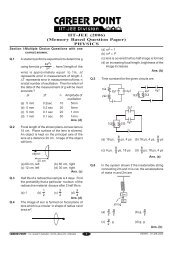
PHYSICS<br />
<strong>1.</strong> Refractive index is maximum for violet and<br />
minimum for red colour<br />
2. Path difference between two waves should be odd<br />
multiple of λ/2 or phase difference between two<br />
waves should be odd multiple of π.<br />
3.<br />
P<br />
−34<br />
h 6.<br />
6 × 10<br />
= =<br />
= <strong>1.</strong>32 × 10<br />
−10<br />
–27 kg-m/s<br />
λ<br />
5000 × 10<br />
4. R = R0A 1/3 ⇒ R ∝ A 1/3<br />
∴<br />
R 1<br />
=<br />
R 2<br />
⎛ A<br />
⎜<br />
⎝ A<br />
3R<br />
∴ R2 =<br />
2<br />
1<br />
2<br />
⎞<br />
⎟<br />
⎠<br />
1<br />
3<br />
⇒<br />
R<br />
=<br />
R 2<br />
1<br />
⎛ 8 ⎞<br />
⎜ ⎟⎠<br />
⎝ 27<br />
/ 3<br />
2<br />
=<br />
3<br />
5. It should be very high i.e. in KHz to GHz<br />
6.<br />
=<br />
µ<br />
c<br />
v ; v2 < v3 < v1<br />
7. Resistivity or specific resistance of a material is<br />
defined as the resistance offered by a wire made by<br />
that material having unit area of cross-section and<br />
unit length.<br />
W<br />
8. V = =<br />
q<br />
MOCK TEST-2 (SOLUTION)<br />
<strong>1.</strong><br />
6×<br />
10<br />
3.<br />
2×<br />
10<br />
– 5<br />
– 7<br />
MOCK TEST– 2 PUBLISHED IN JANUARY ISSUE<br />
= 50 volt<br />
9. Objective lens must have greater focal length than<br />
eye-piece because magnifying power of lens<br />
⎛ f ⎞<br />
⎜ 0 ⎟<br />
⎜<br />
M P =<br />
⎟<br />
increases in this case.<br />
⎝ fe<br />
⎠<br />
10. Conditions of interference<br />
(i) waves must travel in the same medium in the<br />
same direction.<br />
(ii) Their frequencies and wavelengths must be<br />
same<br />
(iii) Their plane of polarisation must be same<br />
(iv) Their must be maintained a constant phase<br />
difference between the waves.<br />
1<strong>1.</strong> Ionisation energy:- Minimum energy required to<br />
remove electron from its ground state.<br />
Excitation energy:- Energy required to transit an<br />
electron to one of its excited state from ground state<br />
KE =<br />
2r<br />
; U = –<br />
∴ U = −2KE<br />
<strong>Xtra</strong><strong>Edge</strong> for IIT-JEE 74 FEBRUARY <strong>2012</strong><br />
KZe 2<br />
12. Emax. = 12V; Emin. = 4V<br />
Ma =<br />
E<br />
E<br />
max<br />
max<br />
− E<br />
+ E<br />
min<br />
min<br />
KZe 2<br />
r<br />
12 − 4<br />
= =<br />
12 + 4<br />
1<br />
2<br />
1<br />
∴ ma in percentage = × 100 = 50%<br />
2<br />
13. Modulating signal being of low frequency cannot<br />
travel to large distance so it is modulated with high<br />
frequency carrier. Frequency modulation is virtually<br />
free from noise where as amplitude modulation<br />
suffers from noise pollution.<br />
14. Semiconductor atoms are tetravalent. The form<br />
covalent bonds by sharing their electrons with the<br />
neighboring atoms. When donor impurity of valency<br />
S is doped, the donor atoms takes the place of a<br />
semiconductor atom in the crystal lattice. Donor<br />
atoms forms covalent bond by sharing its four<br />
electrons whereas the fifth electron of donor atom is<br />
so loosely attached to the atom such that it behaves<br />
as a free electron at room temperature.<br />
15. (i) width of depletion layer of zener diode<br />
becomes very small due to heavy doping of<br />
p and n regions.<br />
(ii) The field across depletion layer becomes very<br />
⎛ V ⎞<br />
high ⎜Q<br />
E = ⎟<br />
⎝ d ⎠<br />
16. Let at any instant charge on the capacitor is q, then<br />
q<br />
p.d. V =<br />
C<br />
Then work done to put additional charge dq is<br />
⎛ q ⎞<br />
dW = (dq) V = ⎜ ⎟ dq<br />
⎝ C ⎠<br />
∴ Total work done to give charge Q is<br />
Q<br />
⎛ q ⎞ Q<br />
W = ∫⎜ ⎟dq =<br />
⎝ C ⎠ 2C<br />
2<br />
1 2<br />
= CV (Q Q = CV)<br />
2<br />
0