Damage formation and annealing studies of low energy ion implants ...
Damage formation and annealing studies of low energy ion implants ... Damage formation and annealing studies of low energy ion implants ...
6.30b). TRIM calculations show the maximum range of the implant and recoil interstitials during a 3 keV As implant does not extend beyond a depth of approximately 20 nm. Therefore any damage from the implant should be well away from the buried oxide interface. MEIS results for the 3 keV As samples showed no significant differences between the bulk, 60 nm and 100 nm SOI samples, (Figure 6.24). Combined with the TRIM results this would lead to the conclusion that when the damage is well away from the BOX and there is a continuous crystalline seed layer the SOI regrowth proceeds in the same fashion as bulk Si, as also seen in (26). a) b) TRIM (A.U.) 1 0.1 0.01 1E-3 1E-4 3keV As TRIM profiles 0 50 100 150 200 250 300 Depth (Ang) As ions Si vacancies Si interstitials Red – As ions Blue – Si Interstitials Green – O interstitials Figure 6.30 a) TRIM results for a 3 keV As implant into Si including vacancy and interstitial profiles. b) Pictorial representation of the TRIM calculation. Results of TRIM calculations for a 40 keV Xe implant are shown in Figure 6.31, likewise the Xe profile and interstitial and vacancy profiles are plotted in Figure 6.31a) 167
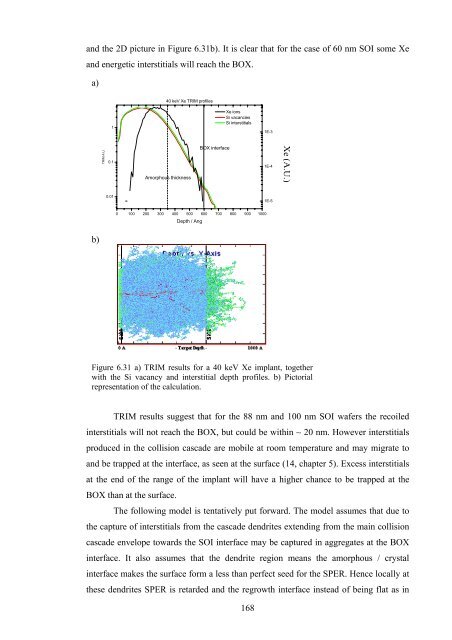
and the 2D picture in Figure 6.31b). It is clear that for the case of 60 nm SOI some Xe and energetic interstitials will reach the BOX. a) b) TRIM A.U. 1 0.1 0.01 40 keV Xe TRIM profiles Amorphous thickness Xe ions Si vacancies Si interstitials 0 100 200 300 400 500 600 700 800 900 1000 Depth / Ang BOX interface Figure 6.31 a) TRIM results for a 40 keV Xe implant, together with the Si vacancy and interstitial depth profiles. b) Pictorial representation of the calculation. TRIM results suggest that for the 88 nm and 100 nm SOI wafers the recoiled interstitials will not reach the BOX, but could be within ~ 20 nm. However interstitials produced in the collision cascade are mobile at room temperature and may migrate to and be trapped at the interface, as seen at the surface (14, chapter 5). Excess interstitials at the end of the range of the implant will have a higher chance to be trapped at the BOX than at the surface. The following model is tentatively put forward. The model assumes that due to the capture of interstitials from the cascade dendrites extending from the main collision cascade envelope towards the SOI interface may be captured in aggregates at the BOX interface. It also assumes that the dendrite region means the amorphous / crystal interface makes the surface form a less than perfect seed for the SPER. Hence locally at these dendrites SPER is retarded and the regrowth interface instead of being flat as in 168 1E-3 1E-4 1E-5 TRIM A.U. Xe (A.U.)
- Page 135 and 136: 5.4 Conclusion MEIS analysis with a
- Page 137 and 138: Chapter 6 Annealing studies 6.1 Int
- Page 139 and 140: 6.2.2.2 Results and Discussion Figu
- Page 141 and 142: theory predictions and X-ray fluore
- Page 143 and 144: implantation conditions are those u
- Page 145 and 146: a) b) c) Yield (counts per 5 µC) Y
- Page 147 and 148: greater than MEIS. SIMS is not sens
- Page 149 and 150: attributed to the interference betw
- Page 151 and 152: The as-implanted sample, with a bro
- Page 153 and 154: a) b) Yield (counts per 5 µC) Yiel
- Page 155 and 156: interface, as evidenced by the high
- Page 157 and 158: duration, is observed. MEIS results
- Page 159 and 160: Yield (counts per 5µC) 500 400 300
- Page 161 and 162: ack edges of the Si peaks are very
- Page 163 and 164: underneath the SiO2 layer, iii) it
- Page 165 and 166: R s (Ω/sq) 950 900 850 800 750 60
- Page 167 and 168: As concentration (at/cm 3 ) 1E22 1E
- Page 169 and 170: R s (Ω/sq) 950 900 850 800 750 70
- Page 171 and 172: Following annealing it was observed
- Page 173 and 174: ∆a/a (x 10 -3 ) 4,0 epi550 3,5 3,
- Page 175 and 176: Yield (counts per 5 uC) 350 300 250
- Page 177 and 178: (FWHM). Concomitantly, As in the re
- Page 179 and 180: Yield (counts per 5 µC) 450 400 35
- Page 181 and 182: The higher temperature anneals carr
- Page 183 and 184: ecomes steeper for the sample annea
- Page 185: Figure 6.28 Schematic illustrations
- Page 189 and 190: 6.5 Conclusion In summary, in this
- Page 191 and 192: 20 L. Capello, T. H. Metzger, M. We
- Page 193 and 194: egarding B profiles relevant to the
- Page 195 and 196: Yield (counts per 5 µC) 400 300 20
- Page 197 and 198: TRIM AU 0.04 0.03 0.02 0.01 TRIM si
- Page 199 and 200: a) F profile PAI 3 keV BF2 b) F pro
- Page 201 and 202: Yield (counts per 5 µC) 20 15 10 5
- Page 203 and 204: the corresponding PAI sample, yield
- Page 205 and 206: amorphous matrix, (16) i.e. local c
- Page 207 and 208: 21 M. Anderle, M. Bersani, D. Giube
- Page 209 and 210: stopped at depths beyond the observ
- Page 211: the role of each individual element
<strong>and</strong> the 2D picture in Figure 6.31b). It is clear that for the case <strong>of</strong> 60 nm SOI some Xe<br />
<strong>and</strong> energetic interstitials will reach the BOX.<br />
a)<br />
b)<br />
TRIM A.U.<br />
1<br />
0.1<br />
0.01<br />
40 keV Xe TRIM pr<strong>of</strong>iles<br />
Amorphous thickness<br />
Xe <strong>ion</strong>s<br />
Si vacancies<br />
Si interstitials<br />
0 100 200 300 400 500 600 700 800 900 1000<br />
Depth / Ang<br />
BOX interface<br />
Figure 6.31 a) TRIM results for a 40 keV Xe implant, together<br />
with the Si vacancy <strong>and</strong> interstitial depth pr<strong>of</strong>iles. b) Pictorial<br />
representat<strong>ion</strong> <strong>of</strong> the calculat<strong>ion</strong>.<br />
TRIM results suggest that for the 88 nm <strong>and</strong> 100 nm SOI wafers the recoiled<br />
interstitials will not reach the BOX, but could be within ~ 20 nm. However interstitials<br />
produced in the collis<strong>ion</strong> cascade are mobile at room temperature <strong>and</strong> may migrate to<br />
<strong>and</strong> be trapped at the interface, as seen at the surface (14, chapter 5). Excess interstitials<br />
at the end <strong>of</strong> the range <strong>of</strong> the implant will have a higher chance to be trapped at the<br />
BOX than at the surface.<br />
The fol<strong>low</strong>ing model is tentatively put forward. The model assumes that due to<br />
the capture <strong>of</strong> interstitials from the cascade dendrites extending from the main collis<strong>ion</strong><br />
cascade envelope towards the SOI interface may be captured in aggregates at the BOX<br />
interface. It also assumes that the dendrite reg<strong>ion</strong> means the amorphous / crystal<br />
interface makes the surface form a less than perfect seed for the SPER. Hence locally at<br />
these dendrites SPER is retarded <strong>and</strong> the regrowth interface instead <strong>of</strong> being flat as in<br />
168<br />
1E-3<br />
1E-4<br />
1E-5<br />
TRIM A.U.<br />
Xe (A.U.)


