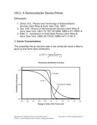
Introduction to radiation-resistant semiconductor devices and circuits
Introduction to radiation-resistant semiconductor devices and circuits
Introduction to radiation-resistant semiconductor devices and circuits

Create successful ePaper yourself
Turn your PDF publications into a flip-book with our unique Google optimized e-Paper software.
contribution (in contrast <strong>to</strong> systems that emphasize noise minimization, as in x-ray<br />
spectrometry or liquid argon calorimetry).<br />
In general, for use in amplifiers bipolar transis<strong>to</strong>r circuitry is superior <strong>to</strong><br />
CMOS. In logic circuitry, especially at low overall switching rates, CMOS is<br />
advantageous both because of power consumption <strong>and</strong> circuit density. For example,<br />
the on-detec<strong>to</strong>r silicon tracker front-end under development for the ATLAS<br />
experiment at the LHC uses bipolar transis<strong>to</strong>r technology for the amplifier-pulse<br />
shaper-compara<strong>to</strong>r <strong>and</strong> <strong>radiation</strong>-hard CMOS for a clock-driven digital pipeline<br />
buffer <strong>and</strong> data readout.<br />
In amplifiers, bipolar transis<strong>to</strong>rs offer higher b<strong>and</strong>width for a given power <strong>and</strong><br />
superior device matching, which is a prime consideration in highly segmented<br />
systems with a correspondingly large number of channels. Threshold shifts in<br />
bipolar transis<strong>to</strong>rs are quite small with excellent matching between <strong>devices</strong>. JFETs<br />
yield excellent noise performance in applications where power consumption <strong>and</strong><br />
circuit density are not prime considerations. Even when a CMOS front-end is<br />
chosen, because of the use of a switched capaci<strong>to</strong>r analog memory, or the desire <strong>to</strong><br />
combine the analog <strong>and</strong> digital circuitry on the same chip, amplifiers can be made<br />
quite <strong>radiation</strong> <strong>resistant</strong>, since the circuitry can be made <strong>to</strong> adjust for shifts in<br />
threshold voltage.<br />
This principle is illustrated by the charge sensitive amplifier in Fig. 8. Transis<strong>to</strong>rs<br />
Q1 - Q4 comprise a cascode gain stage feeding a source follower Q6. Transis<strong>to</strong>rs<br />
Q7 - Q10 perform level shifting <strong>and</strong> biasing. CF <strong>and</strong> Q11 form the feedback<br />
network. Q11 can be utilized either as a resis<strong>to</strong>r or a switch. When biased as a<br />
resis<strong>to</strong>r (RF), the time constant CFRF is chosen <strong>to</strong> be much larger than the rise time.<br />
Q11 also provides continuous DC feedback <strong>to</strong> bias the gate of the input transis<strong>to</strong>r<br />
Q1. When Q11 is used as a switch, it is closed periodically <strong>to</strong> discharge the feedback<br />
capaci<strong>to</strong>r CF <strong>and</strong> also provides DC feedback.<br />
The critical parameter that must be controlled <strong>to</strong> maintain the noise <strong>and</strong> speed<br />
of the amplifier is the transconductance of the input transis<strong>to</strong>r. This in turn is<br />
determined by the drain current in Q1, <strong>and</strong> the biasing circuit must be designed <strong>to</strong><br />
provide the appropriate gate voltage <strong>to</strong> maintain this bias current even as the<br />
required voltage changes with ir<strong>radiation</strong>. This is accomplished by the current<br />
mirror Q4 - Q5, implemented as a matched pair. The desired drain current is<br />
applied as an external control bias current ICASC, which is mirrored <strong>to</strong> the cascode.<br />
The DC feedback through Q11 adjusts the gate voltage of Q1 <strong>to</strong> maintain this current.<br />
Even if the MOSFET threshold voltages change substantially with <strong>radiation</strong>,<br />
this circuit will still maintain the correct current, <strong>to</strong> the extent that the parameters<br />
of the mirror transis<strong>to</strong>rs Q4 <strong>and</strong> Q5 track. This scheme does not maintain the DC<br />
output level, so baseline shifts must be corrected for by correlated double sampling<br />
23