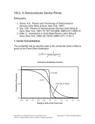
Introduction to radiation-resistant semiconductor devices and circuits
Introduction to radiation-resistant semiconductor devices and circuits
Introduction to radiation-resistant semiconductor devices and circuits

You also want an ePaper? Increase the reach of your titles
YUMPU automatically turns print PDFs into web optimized ePapers that Google loves.
Junction Field Effect Transis<strong>to</strong>rs (JFETs)<br />
JFETs (either silicon or GaAs) can be quite insensitive <strong>to</strong> both ionization <strong>and</strong><br />
displacement effects. In these <strong>devices</strong> a conducting channel from the source <strong>to</strong> the<br />
drain is formed by appropriate doping, typically n type. The gate electrode is<br />
doped p type so that applying a reverse bias voltage relative <strong>to</strong> the channel will<br />
form a depletion region that changes the cross section of the conducting channel.<br />
(31) At low values of gate <strong>and</strong> drain voltages the channel is contiguous <strong>and</strong><br />
resistive. At higher voltage levels the channel becomes fully depleted near the<br />
drain, but the current flow is still determined by the conducting channel near the<br />
source. Since the gate voltage now controls both the geometry <strong>and</strong> potential<br />
distribution, voltage-current characteristics become more complex <strong>and</strong> the device<br />
acts much like a controlled current source, i.e. it exhibits a high output resistance.<br />
With respect <strong>to</strong> <strong>radiation</strong> effects, the important fact is that device characteristics<br />
are determined essentially by the geometry <strong>and</strong> doping level of the channel.<br />
Typical doping levels are 10 15 <strong>to</strong> 10 18 cm -3 , so the effect of <strong>radiation</strong>-induced<br />
accep<strong>to</strong>r states is small. Silicon JFETs exhibit very good <strong>radiation</strong> resistance.<br />
Measurements on both st<strong>and</strong>ard commercial <strong>devices</strong> <strong>and</strong> cus<strong>to</strong>m designed integrated<br />
<strong>circuits</strong> have shown minimal changes in gain at fluences >10 14 neutrons/cm 2<br />
<strong>and</strong> ionization doses up <strong>to</strong> 100 Mrad. (32,33,34). Low frequency noise<br />
(f < 100 kHz) may increase by an order of magnitude, but at high frequencies very<br />
little change in noise is observed. Measurements of Si JFETs at 90K also exhibit<br />
excellent <strong>radiation</strong> characteristics. (33)<br />
In some applications, analog s<strong>to</strong>rage circuitry for example, gate leakage<br />
current is important. Generation current in the gate depletion region due <strong>to</strong><br />
displacement damage can affect the gate current strongly. Measurements on<br />
commercial JFETs irradiated by high-energy electrons <strong>to</strong> 100 Mrad (Φ≈ 10 15 cm -2 )<br />
show the gate reverse current increasing 100 fold from an initial value of 70 pA.<br />
(35) Here one should choose the smallest geometry device commensurate with<br />
other requirements.<br />
At this point it is worth noting that the superior <strong>radiation</strong> resistance claimed for<br />
GaAs ICs has more <strong>to</strong> do with the use of JFETs or MESFETs (a Schottky barrier<br />
JFET) than the properties of the semiconduc<strong>to</strong>r. These <strong>devices</strong> are more <strong>radiation</strong><br />
<strong>resistant</strong> than silicon MOSFETs (discussed below), but suffer from a much lower<br />
circuit density.<br />
15