

The Do's and Don'ts of Using MOS - International Rectifier
The Do's and Don'ts of Using MOS - International Rectifier
The Do's and Don'ts of Using MOS - International Rectifier

You also want an ePaper? Increase the reach of your titles
YUMPU automatically turns print PDFs into web optimized ePapers that Google loves.
APPLICATION NOTE<br />
In this application note, some <strong>of</strong> the most common do’s <strong>and</strong> don’ts <strong>of</strong> using HEXFET ® power <strong>MOS</strong>FETs are described.<br />
<strong>The</strong> objective is to help the user get the most out <strong>of</strong> these remarkable devices, while reducing “on the job” learning time<br />
to a minimum.<br />
1. Be Mindful <strong>of</strong> <strong>The</strong> Reverse Blocking Characteristics <strong>of</strong> <strong>The</strong> Device<br />
IGBTs have a limited reverse blocking capability <strong>of</strong> approximately<br />
20-30 V, with high leakage. This is characterized in IR’s data<br />
sheets with a Reverse Avalanche Energy (EARV). This rating is<br />
useful to absorb energy spikes due to the stray inductance in series<br />
with the anti-parallel diode. This is a significant advantage over<br />
bipolar transistors <strong>and</strong> power darlingtons. A feature <strong>of</strong> power<br />
<strong>MOS</strong>FETs is that they inherently have built into them an integral<br />
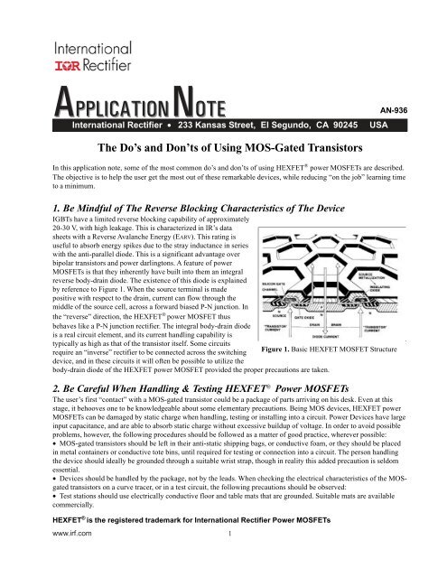
reverse body-drain diode. <strong>The</strong> existence <strong>of</strong> this diode is explained<br />
by reference to Figure 1. When the source terminal is made<br />
positive with respect to the drain, current can flow through the<br />
middle <strong>of</strong> the source cell, across a forward biased P-N junction. In<br />
the “reverse” direction, the HEXFET ® power <strong>MOS</strong>FET thus<br />
behaves like a P-N junction rectifier. <strong>The</strong> integral body-drain diode<br />
is a real circuit element, <strong>and</strong> its current h<strong>and</strong>ling capability is<br />
typically as high as that <strong>of</strong> the transistor itself. Some circuits<br />
require an “inverse” rectifier to be connected across the switching<br />
device, <strong>and</strong> in these circuits it will <strong>of</strong>ten be possible to utilize the<br />
body-drain diode <strong>of</strong> the HEXFET power <strong>MOS</strong>FET provided the proper precautions are taken.<br />
2. Be Careful When H<strong>and</strong>ling & Testing HEXFET ® Power <strong>MOS</strong>FETs<br />
<strong>The</strong> user’s first “contact” with a <strong>MOS</strong>-gated transistor could be a package <strong>of</strong> parts arriving on his desk. Even at this<br />
stage, it behooves one to be knowledgeable about some elementary precautions. Being <strong>MOS</strong> devices, HEXFET power<br />
<strong>MOS</strong>FETs can be damaged by static charge when h<strong>and</strong>ling, testing or installing into a circuit. Power Devices have large<br />
input capacitance, <strong>and</strong> are able to absorb static charge without excessive buildup <strong>of</strong> voltage. In order to avoid possible<br />
problems, however, the following procedures should be followed as a matter <strong>of</strong> good practice, wherever possible:<br />
• <strong>MOS</strong>-gated transistors should be left in their anti-static shipping bags, or conductive foam, or they should be placed<br />
in metal containers or conductive tote bins, until required for testing or connection into a circuit. <strong>The</strong> person h<strong>and</strong>ling<br />
the device should ideally be grounded through a suitable wrist strap, though in reality this added precaution is seldom<br />
essential.<br />
• Devices should be h<strong>and</strong>led by the package, not by the leads. When checking the electrical characteristics <strong>of</strong> the <strong>MOS</strong>gated<br />
transistors on a curve tracer, or in a test circuit, the following precautions should be observed:<br />
• Test stations should use electrically conductive floor <strong>and</strong> table mats that are grounded. Suitable mats are available<br />
commercially.<br />
www.irf.com<br />
<strong>International</strong> <strong>Rectifier</strong> • 233 Kansas Street, El Segundo, CA 90245<br />
<strong>The</strong> Do’s <strong>and</strong> Don’ts <strong>of</strong> <strong>Using</strong> <strong>MOS</strong>-Gated Transistors<br />
1<br />
USA<br />
AN-936<br />
Figure 1. Basic HEXFET <strong>MOS</strong>FET Structure<br />
HEXFET ® is the registered trademark for <strong>International</strong> <strong>Rectifier</strong> Power <strong>MOS</strong>FETs
AN-936 (v.Int)<br />
• When inserting the device in a curve tracer or a test circuit, voltage should not be applied until all terminals are solidly<br />
connected into the circuit.<br />
• When using a curve tracer, a resistor should be connected in series with the gate to damp spurious oscillations that can<br />
otherwise occur on the trace. A suitable value <strong>of</strong> resistance is 100 ohms.<br />
• For repeated testing, it is convenient to build this resistor into the test fixture.<br />
• When switching from one test range to another, voltage <strong>and</strong> current settings should be reduced to zero, to avoid the<br />
generation <strong>of</strong> potentially destructive voltage surges during switching.<br />
<strong>The</strong> next step is to connect the device into an actual circuit. <strong>The</strong> following simple precautions should be observed:<br />
• Work stations should use electrically grounded table <strong>and</strong> floor mats.<br />
• Soldering irons should be grounded.<br />
Now that the device has been connected into its circuit, it is ready for the power to be applied. From here on, success in applying<br />
the device becomes a matter <strong>of</strong> the integrity <strong>of</strong> the circuit design, <strong>and</strong> <strong>of</strong> what circuit precautions have been taken to guard<br />
against unintentional abuse <strong>of</strong> its ratings.<br />
<strong>The</strong> following are the interrelated device <strong>and</strong> circuit considerations that lead to reliable, trouble-free design.<br />
3. BEWARE OF UNEXPECTED GATE-TO-SOURCE VOLTAGE SPIKES<br />
Excessive voltage will punch through the gate-source oxide layer <strong>and</strong> result in permanent damage. This seems obvious enough,<br />
but it is not so obvious that transient gate-to-source overvoltages can be generated that are quite unrelated to, <strong>and</strong> well in excess<br />
<strong>of</strong>, the amplitude <strong>of</strong> the applied drive signal. <strong>The</strong> problem is illustrated by reference to Figure 2.<br />
If we assume that the impedance, Z, <strong>of</strong> the drive source is high, then any positive-going change <strong>of</strong> voltage applied across the<br />
drain <strong>and</strong> source terminals (caused, for example, by the switching <strong>of</strong> another device in the circuit) will be reflected as a positivegoing<br />
voltage transient across the source <strong>and</strong> the drain terminals, in the approximate ratio <strong>of</strong>:<br />
1<br />
1+ C<br />
C<br />
gs<br />
dg<br />
<strong>The</strong> above ratio is typically about 1 to 6. This means that a change <strong>of</strong> drain-to-source voltage <strong>of</strong> 300V, for example, could<br />
produce a voltage transient approaching 50V between the gate <strong>and</strong> source terminals. In practice this “aiming” voltage will not<br />
appear on the gate if the dv/dt is positive because the <strong>MOS</strong>-gated device goes in conduction at approximately Vgs = 4V, thereby<br />
clamping the dv/dt at the expense <strong>of</strong> a current transient <strong>and</strong> increased power dissipation. However, a negative-going dv/dt will<br />
not be clamped. This calculation is based upon the worst case assumption that the transient impedance <strong>of</strong> the drive circuit is high<br />
by comparison with the gate-to-source capacitance <strong>of</strong> the device. This situation can, in fact, be quite easily approximated if the<br />
gate drive circuit contains inductance—for example the leakage inductance <strong>of</strong> an isolating drive transformer. This inductance<br />
exhibits a high impedance for short transients, <strong>and</strong> effectively decouples the gate from its drive circuit for the duration <strong>of</strong> the<br />
transient.<br />
<strong>The</strong> negative-going gate-to-source voltage transient produced under the above circumstances may exceed the gate voltage rating<br />
<strong>of</strong> the device, causing permanent damage. It is, <strong>of</strong> course, true that since the applied drain transient results in a voltage at the<br />
gate which tends to turn the device ON, the overall effect is to an extent self-limiting so far as the gate voltage transient is<br />
concerned. Whether this self-limiting action will prevent the voltage transient at the gate from exceeding the gate-source voltage<br />
rating <strong>of</strong> the device depends upon the impedance <strong>of</strong> the external circuit. Spurious turn-on is <strong>of</strong> itself undesirable, <strong>of</strong> course,<br />
though in practical terms one may grudgingly be able to accept this circuit operating imperfection, provided the safe operating<br />
area <strong>of</strong> the device is not violated.<br />
Notice that a voltage clamp (a conventional zener diode is suitable for this purpose) to prevent the gate-source voltage rating<br />
from being exceeded will not prevent the dv/dt induced turn-on, as the gate will not reach the zener voltage. In many instances<br />
the zener is responsible for generating oscillations in the gate circuit, particularly when a significant amount <strong>of</strong> stray inductance<br />
is present. A more fundamental solution, <strong>of</strong> course, is to make the impedance <strong>of</strong> the gate circuit low enough that not only is the<br />
gate-source voltage rating not exceeded, but also the voltage transient at the gate is contained to a level at which spurious turn-on<br />
does not occur.
"POSITIVE<br />
GOING"<br />
CHANGE<br />
+E<br />
DRAIN-SOURCE<br />
VOLTAGE<br />
"NEGATIVE GOING"<br />
CHANGE<br />
WITH NO<br />
CLAMPING GATE-SOURCE<br />
VOLTAGE<br />
WITH NO<br />
CLAMPING<br />
DRIVE<br />
SOURCE<br />
IMPEDANCE<br />
AN-936 (v.Int)<br />
It should be remembered that a collapse <strong>of</strong> voltage across the device (i.e., a negative-going dv/dt) will produce a transient<br />
negative voltage spike across the gate-source terminals. In this case, <strong>of</strong> course, there will be no tendency for the device to turn<br />
ON, <strong>and</strong> hence no tendency for the effect to be self-limiting. A zener diode connected to clamp positive transients will<br />
automatically clamp negative-going transients, limiting them to the forward conduction voltage drop <strong>of</strong> the zener.<br />
Z<br />
C DG<br />
G<br />
C GS<br />
EXTERNALLY CONNECTED<br />
CLAMPING ZENER DIODE<br />
Figure 2. A Rapidly Changing Applied Drain-Source Voltage will Produce Gate-Source Transients<br />
(a) UNCLAMPED<br />
INDUCTIVE<br />
LOAD<br />
R<br />
L<br />
OVERVOLTAGE<br />
TRANSIENT<br />
DUE TO L<br />
Figure 3. Drain-Source Overvoltage Transient when<br />
Switching Off with Unclamped Inductive Load<br />
+E<br />
L S<br />
(b) CLAMPED<br />
INDUCTIVE<br />
LOAD<br />
LS = STRAY CIRCUIT<br />
INDUCTANCE<br />
L S D<br />
S<br />
R<br />
L<br />
L S<br />
V DS<br />
D<br />
S<br />
C DS<br />
OVERVOLTAGE<br />
TRANSIENT<br />
DUE TO L S<br />
Figure 4. Drain-Source Overvoltage Transient<br />
Produced by Stray Circuit Inductance When Switching<br />
Off with Clamped, Inductive Load<br />
E
AN-936 (v.Int)<br />
4. BEWARE OF DRAIN OR COLLECTOR VOLTAGE SPIKES INDUCED BY<br />
SWITCHING<br />
<strong>The</strong> uninitiated designer is <strong>of</strong>ten not aware that self-inflicted overvoltage transients can be produced when the device is switched<br />
OFF, even though the DC supply voltage for the drain circuit is well below the VDS rating <strong>of</strong> the transistor.<br />
Figure 3 shows how a voltage spike is produced when switching the device OFF, as a result <strong>of</strong> inductance in the circuit. <strong>The</strong><br />
faster the device is switched, the higher the overvoltage will be.<br />
Inductance is always present to some extent in a practical circuit, <strong>and</strong> therefore, there is always danger <strong>of</strong> inducing overvoltage<br />
transients when switching OFF. Usually, <strong>of</strong> course, the main inductive component <strong>of</strong> the load will be "clamped", as shown in<br />
Figure 4. Stray circuit inductance still exists, however, <strong>and</strong> overvoltage transients will still be produced as a result—to say<br />
nothing <strong>of</strong> the fact that the clamping diode may not provide an instantaneous clamping action, due to its "forward recovery"<br />
characteristic.<br />
<strong>The</strong> first approach to this problem is to minimize stray circuit inductance, by means <strong>of</strong> careful attention to circuit layout, to the<br />
point that whatever residual inductance is left in the circuit can be tolerated. HEXFET ® s have an inductive energy rating that<br />
makes capable <strong>of</strong> withst<strong>and</strong>ing these inductive spikes, assuming that the data sheet limits for energy <strong>and</strong> temperature are not<br />
violated. IGBTs, however, do not have an avalanche rating, <strong>and</strong> a clamping device should be connected, physically as close as<br />
possible to the drain <strong>and</strong> source terminals, as shown in Figure 5. A conventional zener diode, or a "transorb" clamping device,<br />
are satisfactory for this purpose. An alternative clamping circuit is shown in Figure 6, depending on the voltage <strong>and</strong> current<br />
rating <strong>of</strong> the circuit.<br />
<strong>The</strong> capacitor C is a reservoir capacitor <strong>and</strong> charges to a substantially constant voltage, while the resistor R is sized to dissipate<br />
the "clamping energy" while maintaining the desired voltage across the capacitor. <strong>The</strong> diode D must be chosen so that its forward<br />
recovery characteristic does not significantly spoil the transient clamping action <strong>of</strong> the circuit. A simple RC snubber can also be<br />
used, as shown in Figure 7. Note, however, that an RC snubber not only limits the peak voltage, it also slows down the effective<br />
switching speed. In so doing, it absorbs energy during the whole <strong>of</strong> the switching period, not just at the end <strong>of</strong> it, as does a<br />
voltage clamp. A snubber is therefore less efficient than a true voltage clamping device.<br />
Note that the highest voltage transient occurs when switching the highest level <strong>of</strong> current. <strong>The</strong> waveform <strong>of</strong> the voltage across the<br />
device should be checked with a high-speed oscilloscope at the full load condition to ensure that switching voltage transients are<br />
within safe limits.<br />
5. DO NOT EXCEED THE PEAK<br />
CURRENT RATING<br />
All power transistors have a specified maximum peak<br />
current rating. This is conservatively set at a level that<br />
guarantees reliable operation <strong>and</strong> it should not be<br />
exceeded. It is <strong>of</strong>ten overlooked that, in a practical<br />
circuit, peak transient currents can be obtained that are<br />
well in excess <strong>of</strong> the expected normal operating current,<br />
unless proper precautions are taken. Heating, lighting<br />
<strong>and</strong> motor loads, for example, consume high in-rush<br />
currents if not properly controlled. A technique that<br />
ensures that the peak current does not exceed the<br />
capability <strong>of</strong> the device is to use a current sensing control<br />
that switches it OFF whenever the current<br />
instantaneously reaches a preset limit.<br />
Unexpectedly high transient current can also be obtained<br />
as a result <strong>of</strong> rectifier reverse recovery, when a transistor<br />
is switched ON rapidly into a conducting rectifier. This is<br />
illustrated in Figure 8. <strong>The</strong> solution is to use a faster<br />
rectifier, or to slow down the switching <strong>of</strong> the transistor<br />
to limit the peak reverse recovery current <strong>of</strong> the rectifier.<br />
6. STAY WITHIN THE THERMAL LIMITS<br />
+E<br />
L S<br />
(c) CLAMPED<br />
INDUCTIVE LOAD<br />
WITH LOCAL D-S<br />
ZENER CLAMP<br />
R<br />
L<br />
L S<br />
D<br />
S<br />
L S<br />
V DS<br />
OVERVOLTAGE<br />
TRANSIENT<br />
CLAMPED<br />
BY ZENER<br />
CLAMPING<br />
ZENER<br />
Figure 5. Overvoltage Transient at Switch-Off Clamped by<br />
Local Drain-Source Zener
Power transistors are thermally limited. <strong>The</strong>y must be<br />
mounted on a heatsink that is adequate to keep the<br />
junction temperature within the rated under the<br />
"worst case" condition <strong>of</strong> maximum power dissipation<br />
<strong>and</strong> maximum ambient temperature.<br />
It must be remembered that in a switching<br />
application, the total power is due to the conduction<br />
losses <strong>and</strong> the switching loss. Switching time <strong>and</strong><br />
switching losses <strong>of</strong> HEXFET ® s are essentially<br />
independent <strong>of</strong> temperature, but the conduction losses<br />
increase with increasing temperature, because RDS(on)<br />
increases with temperature. IGBTs, on the contrary,<br />
have switching losses that highly dependent <strong>of</strong><br />
temperature, while conduction losses are not. This<br />
must be taken into account when sizing the heatsink.<br />
<strong>The</strong> required thermal resistance <strong>of</strong> the heatsink can<br />
be calculated as follows:<br />
<strong>The</strong> transistor conduction power, PT, is given<br />
approximately by PT = On-state Voltage x Drain or<br />
Collector current<br />
<strong>The</strong> switching energy depends upon the voltage <strong>and</strong><br />
current being switched <strong>and</strong> the type <strong>of</strong> load. <strong>The</strong> total<br />
switching loss, PS, is the total switching energy, εT,<br />
multiplied by the operating frequency, f. eT is the sum<br />
<strong>of</strong> the energies due to the individual switchings that<br />
take place in each fundamental operating cycle:<br />
PS = εT f<br />
<strong>The</strong> total power dissipation is the sum <strong>of</strong> the conduction power, PT, <strong>and</strong> the switching power, PS.<br />
Since:<br />
P = PT + PS<br />
ΔTJA = PRth<br />
where:<br />
Rth = junction-to-ambient thermal<br />
resistance<br />
<strong>The</strong> junction-to-ambient thermal resistance, RJA,<br />
is made up <strong>of</strong> the internal junction-to-case<br />
thermal resistance, RJC, plus the case-toheatsink<br />
thermal resistance, RCS, plus the sinkto-ambient<br />
thermal resistance, RSA. <strong>The</strong> first<br />
two terms are fixed for the device, <strong>and</strong> the<br />
required thermal resistance <strong>of</strong> the heatsink, RS-<br />
A, for a given junction temperature rise DTJ-A,<br />
can be calculated from:<br />
RS-A = RJ-A - (RJC + RC-S)<br />
7. PAY ATTENTION TO CIRCUIT LAYOUT<br />
+E<br />
0<br />
+E<br />
E C<br />
E<br />
AN-936 (v.Int)<br />
Figure 6. Overvoltage Transient at Switch-Off Limited by<br />
Local Clamp<br />
L S<br />
R<br />
L<br />
L S<br />
D<br />
S<br />
L S<br />
D<br />
E C<br />
C<br />
OVERVOLTAGE TRANSIENT<br />
REDUCED BY SNUBBER<br />
V DS<br />
(d) CLAMPED INDUCTIVE<br />
LOAD WITH LOCAL<br />
D-S SNUBBER<br />
SNUBBER<br />
Figure 7. Overvoltage Transient at Switch-Off Limited by Local<br />
Capacitor-Resistor Snubber<br />
R<br />
E
AN-936 (v.Int)<br />
Stray inductance in the circuit can cause overvoltage transients, slowing down <strong>of</strong> the switching speed, unexpected unbalance <strong>of</strong><br />
current between parallel connected devices, <strong>and</strong> unwanted oscillations.<br />
In order to minimize these effects, stray circuit inductance must be minimized. This is done by keeping conduction paths as short<br />
as possible, by minimizing the area <strong>of</strong> current loops, by using twisted pairs <strong>of</strong> leads, <strong>and</strong> by using ground plane construction.<br />
Local decoupling capacitors alleviate the affects <strong>of</strong> any residual circuit inductance, once these measures have been taken.<br />
Circuit layout should be kept as symmetrical as possible in order to maintain balanced currents in parallel connected HEXFET ® s<br />
or IGBTs. <strong>The</strong> gates <strong>of</strong> parallel connected devices should be decoupled by small ferrite beads placed over the gate connections, or<br />
by individual resistors in series with each gate. <strong>The</strong>se measures prevent parasitic oscillations.<br />
8. BE CAREFUL WHEN USING THE INTEGRAL BODY-DRAIN DIODE<br />
<strong>The</strong> HEXFET ® 's integral body-drain diode exhibits<br />
minority carrier reverse recovery. Reverse recovery presents<br />
a potential problem when switching any rectifier <strong>of</strong>f;<br />
the slower the rectifier, the greater the problem. By<br />
comparison with the HEXFET ® itself, the switching speed<br />
<strong>of</strong> the integral reverse rectifier is quite slow. <strong>The</strong> switching<br />
speed <strong>of</strong> a circuit which utilizes the body-drain diode <strong>of</strong> the<br />
HEXFET ® may therefore be limited by the rectifier.<br />
Whether this will be so depends upon the circuit <strong>and</strong> the<br />
operating conditions.<br />
Regardless <strong>of</strong> the overall circuit configuration, or the<br />
particular application, the "local" circuit operating<br />
situation that is troublesome occurs when the freewheeling<br />
current from an inductive load is commutated from the<br />
integral rectifier <strong>of</strong> one HEXFET ® to the transistor <strong>of</strong> an<br />
"opposite" HEXFET ® , the two devices forming a t<strong>and</strong>em<br />
series connected pair across a low impedance voltage<br />
source, as shown in Figure 8. This “local” circuit<br />
configuration occurs in most chopper <strong>and</strong> inverter<br />
schemes.<br />
If the incoming HEXFET ® switches ON too rapidly, the<br />
peak reverse recovery current <strong>of</strong> the integral body-drain<br />
diode <strong>of</strong> the opposite HEXFET ® will rise too rapidly, the<br />
peak reverse recovery current rating will be exceeded, <strong>and</strong><br />
the device may possibly be destroyed.<br />
<strong>The</strong> peak reverse recovery current <strong>of</strong> the rectifier can be reduced by slowing down the rate <strong>of</strong> change <strong>of</strong> current during the<br />
commutation process. <strong>The</strong> rate <strong>of</strong> change <strong>of</strong> current can be controlled by purposefully slowing down the rate <strong>of</strong> rise <strong>of</strong> the gate<br />
driving pulse. <strong>Using</strong> this technique, the peak current can be reduced to almost any desired extent, at the expense <strong>of</strong> prolonging<br />
the high dissipation switching period.<br />
<strong>The</strong> oscillograms in Figure 9 illustrate the effect. By slowing the total switch-ON time from 300ns to 1.8ms, the peak current <strong>of</strong><br />
the IRF330 has been decreased from 20A to 10A. <strong>The</strong> energy dissipation associated with the “unrestrained” switch-ON in Figure<br />
9(a) is 0.9mJ, whereas it is 2.7mJ for the controlled switch-ON <strong>of</strong> Figure 9(b).<br />
Note also that it is not necessary to slow the switching-OFF <strong>of</strong> the HEXFET ® , hence the energy dissipation at switch-OFF will be<br />
relatively small by comparison with that at switch-ON. For operation at frequencies up to a few kHz, where ultra-fast switching is<br />
not m<strong>and</strong>atory, slowing the applied gate drive signal to reduce the peak reverse recovery current <strong>of</strong> the "opposite" rectifier <strong>of</strong>fers<br />
a good practical solution.<br />
I<br />
I<br />
IF:<br />
INDUCTIVE LOAD<br />
CURRENT IS<br />
FREE-WHEELING<br />
IN THE<br />
BODY-DRAIN<br />
DIODE OF<br />
THIS DEVICE<br />
THEN:<br />
TAKE CARE WHEN<br />
SWITCHING-ON<br />
THIS DEVICE<br />
Figure 8. Local Circuit Configuration <strong>and</strong> Operating<br />
Condition Requiring Special Care When <strong>Using</strong> the<br />
HEXFET's Integral Body-Drain Diode.
AN-936 (v.Int)<br />
9. BE ON YOUR GUARD WHEN COMPARING CURRENT RATINGS<br />
<strong>The</strong> user can be forgiven if he assumes that the continuous drain current rating, that appears on the data sheet represents the<br />
current at which the device can actually be operated continuously in a practical system. To be sure, that's what it should<br />
represent; unfortunately it <strong>of</strong>ten does not.<br />
Frequently a "continuous" current rating is assigned to the device which in practical terms cannot be used, because the resulting<br />
conduction power dissipation would be so large as to require a heatsink with an impractically low thermal resistance, <strong>and</strong>/or an<br />
impractically low ambient operating temperature. <strong>The</strong> best advice to the user is to compare different types on the basis <strong>of</strong> high<br />
temperature conduction <strong>and</strong> switching losses, <strong>and</strong> not <strong>of</strong> current rating. For <strong>MOS</strong>FETS, it is sufficient to compare RDS(on) at 25°<br />
C, <strong>and</strong> this provides a common basis for comparison. This parameter, taken in conjunction with the junction-case thermal<br />
resistance, is a much better indication <strong>of</strong> the power <strong>MOS</strong>FET true current h<strong>and</strong>ling capability.<br />
100V<br />
10mV<br />
(a) I (max) = 20A, di/dt = 50A/ms.<br />
Switching time = 300nsec.<br />
2μS<br />
10mV<br />
(b) I<br />
(max)<br />
= 20A, di/dt = 50A/μ /μs.<br />
Switching time = 1.8 ms..<br />
Figure 9. Oscillograms <strong>of</strong> IRF330 Switching into Reverse <strong>Rectifier</strong> <strong>of</strong> Another IRF330 with Freewheeling<br />
Current <strong>of</strong> 4A.<br />
Top Trace: Voltage 100V/div.<br />
Bottom Trace: Current 4A/div.<br />
Time Scale: 2ms/div.<br />
2μS


