Polymer Devices : Materials, Physics, Technology & Circuits - Silvaco
Polymer Devices : Materials, Physics, Technology & Circuits - Silvaco
Polymer Devices : Materials, Physics, Technology & Circuits - Silvaco

You also want an ePaper? Increase the reach of your titles
YUMPU automatically turns print PDFs into web optimized ePapers that Google loves.
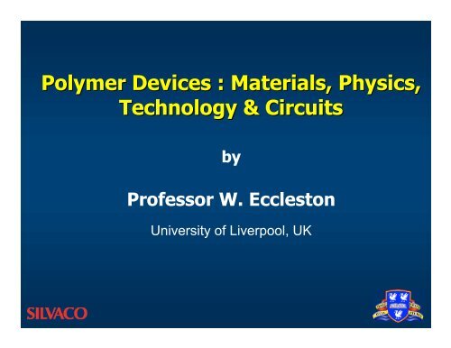
<strong>Polymer</strong> <strong>Devices</strong> : <strong>Materials</strong>, <strong>Physics</strong>,<br />
<strong>Technology</strong> & <strong>Circuits</strong><br />
by<br />
Professor W. Eccleston<br />
University of Liverpool, UK
Ahmed Nejim<br />
Simon Higgins<br />
Naser Sedghi<br />
Munira Raja<br />
Giles Lloyd<br />
Kevin Molloy<br />
Rafaella Di Lucrezia
Summary of talk<br />
ß applications and markets<br />
ß basic polymer conduction properties<br />
ß Schottky diodes<br />
ß light emitting diodes<br />
ß thin film transistors (TFTs/PFETs)<br />
ß circuits<br />
ß European picture
Basic <strong>Polymer</strong> (P3HT) Properties<br />
• usually p - type<br />
• hole mobility low<br />
• soluble in cheap solvents<br />
• can be spun or ink-jetted when dissolved<br />
• photolithography difficult<br />
• tend to be unstable
• Moore’s Law: the problem with silicon<br />
• only designs for speed<br />
• transistors and circuits get smaller each<br />
year<br />
• most applications have to be ‘man-sized’<br />
• markets require ultra-low cost<br />
• large area<br />
• disposable electronics
The Market Sphere<br />
increasing speed sector<br />
(silicon)<br />
Other sectors :<br />
• advertising<br />
• displays<br />
• security<br />
• retail<br />
• electronic newsprint<br />
• etc.
MEURO<br />
10 5<br />
10 4<br />
10 3<br />
10 2<br />
2002<br />
W. European market<br />
10<br />
0 5 10 15 20 25 30<br />
1<br />
Years<br />
• RF retail tags<br />
• Security documents<br />
• Flexible roll-up displays
Large area electronics<br />
• flat panel/roll-up displays<br />
• electronic newspapers<br />
• medical imaging<br />
• electronic bar codes (rf tags)<br />
• security documents<br />
e.g. building access, luggage tracking labels<br />
• active signage/advertising hoardings<br />
etc
Comparison of technologies (MOS)<br />
implant<br />
doped poly<br />
gate oxide<br />
metal<br />
CMOS<br />
deposited<br />
oxide<br />
Epitaxy<br />
or implant<br />
single<br />
crystal<br />
silicon
Comparison of technologies<br />
metal<br />
Ink-jetted or spun polymer<br />
Aluminium on flexible plastic<br />
gate<br />
oxide
<strong>Polymer</strong> <strong>Technology</strong><br />
• easy to synthesise polymers<br />
• easy to apply<br />
• ultra- low cost flexible substrates<br />
• vast range of materials<br />
• good Schottky diodes<br />
• no interface states<br />
• low mobility, high capacitance, therefore slow<br />
• no p-n junctions<br />
• air / voltage/ light /dopant/ instability
<strong>Polymer</strong> conduction processes ?<br />
• Role of dopants<br />
• Fowler - Nordheim<br />
• Schottky Emission<br />
• Poole - Frenkel<br />
• Ohmic Poole Frenkel<br />
• Ohmic<br />
• Free Space Charge Limited<br />
• Trap Space Charge Limited
hole<br />
hole<br />
Fowler-Nordheim<br />
or Schottky emission<br />
Poole-Frenkel or Trap<br />
SCLC when trap<br />
density very high
Method of doping : replacing ion implantation<br />
polymer dopant polymer + dopant
Key Role of Dopants
Air / Voltage/ Light / Dopant/ instability<br />
Output characteristics of P3HT TFT with aspect ratio of 133.
Current through gate oxide (Al 2O3) ) demonstrated<br />
with high dopant content<br />
I-V characteristics of<br />
P3HT MOS capacitor.<br />
(a) no polymer,<br />
(b) polymer removed,<br />
(c) no dopant,<br />
(d) 1% dopant and<br />
(e) 5% dopant.
Mechanism ?<br />
gate oxide<br />
Metal gate<br />
dopant<br />
I<br />
+ V G<br />
• dopant ions break free<br />
from polymer chains<br />
• induces positive<br />
charge in the gate<br />
• current flow into gate<br />
I = displacement current
Capacitance Voltage (CV) Plots for P3HT MOSC<br />
• typical of mobile<br />
charge in oxide but<br />
must be charge in<br />
polymer<br />
• ratio of C max/C min<br />
gives doping density<br />
• flat C min ??
Importance of Cmin min<br />
V G+dV G<br />
depletion region<br />
gate<br />
gate<br />
insulator<br />
A<br />
<strong>Polymer</strong> P3HT<br />
electrons or ions<br />
• constant C min means<br />
constant depletion<br />
layer width<br />
• constant depletion<br />
region requires<br />
formation of negative<br />
layer at interface<br />
• mobility of negative ?<br />
found to be greater<br />
than: 10 -7 cm 2 V -1 s 1<br />
• is it electrons or<br />
ions?
Other parameters from CV plots on polymers<br />
• failure to deliver<br />
holes to surface<br />
region in<br />
accumulation<br />
• hole mobility<br />
10 -2 cm 2 V -1 s -1
Revision of Properties<br />
• hole mobility: 10 -2 cm 2 V -1 s -1<br />
• electron mobility very low: 10 -5 cm 2 V -1 s -1<br />
• doping level can be varied from 10 15 to 10 18 cm -3<br />
• mobile dopant a problem<br />
• hole mobility depends strongly on dopant<br />
concentration
Effects of mobile dopant on devices (e.g. TFTs) TFTs<br />
Transfer characteristics<br />
for P3HT TFT with<br />
aspect ratio of 133,<br />
(a) 1mm film heavily<br />
doped,<br />
(b) 0.5 mm film heavily<br />
doped and<br />
(c) 5 nm film heavily<br />
doped.
<strong>Polymer</strong> Schottky Diodes<br />
aluminium<br />
E F<br />
depletion<br />
polymer<br />
gold<br />
E C<br />
E V
Reverse biased polymer Schottky diode<br />
V applied<br />
Al<br />
E F<br />
E C<br />
EF EV V B enhances hole<br />
injection from<br />
metal
E F<br />
ITO<br />
e<br />
image charge<br />
E V<br />
h<br />
Fowler- Nordheim<br />
electron injection at<br />
cathode to produce<br />
holes
E V<br />
reduced barrier to holes<br />
V forward<br />
Log e (I )<br />
I µ exp (qV forward/kT)<br />
V forward
I-V characteristics of P3HT Schottky diodes<br />
(a) Purified P3HT,<br />
(b) as-synthesised<br />
P3HT and<br />
(c) doped P3HT<br />
Purified material<br />
gives lowest currents<br />
lowest mobility !
Measuring mobility by Liverpool method<br />
• measure doping<br />
N A from reverse<br />
current<br />
• measure<br />
conductivity s<br />
from forward<br />
current<br />
• s = N Ae m<br />
• hence m can be<br />
found
Mobility dependency on doping density<br />
• P3HT<br />
• applies to all<br />
other polymers<br />
tested<br />
•can increase m<br />
by doping<br />
•causes<br />
instability
Basic Relationships :<br />
m = 10 -73 N A 2.35<br />
m FE = 10 -71 N A 2.35 from TFTs<br />
s = 10 -73 N A 3.35<br />
apply over many orders of magnitude of<br />
doping
<strong>Polymer</strong> LEDs
Preferred materials for PLEDs<br />
• PPV (hole transport layer)<br />
• Cyano-PPV (electron transport layer)<br />
• iridium complexes (Covion)<br />
• indium tin oxide (transparent cathode)<br />
• Ca (high cost anode)<br />
• Al (low cost anode, poor emitter, forms oxide)<br />
• Al : Li (good anode, high cost)
Single Layer Diode<br />
• electron efficiency<br />
poor: large barrier, low<br />
mobility.<br />
• recombination at the<br />
Schottky diode?<br />
• low efficiency
Double Layer Diode<br />
• electron efficiency<br />
better: smaller barrier,<br />
• recombination at the<br />
Schottky diode?<br />
• improved efficiency<br />
adds 1% to single layer<br />
device<br />
• metal contacts nonideal<br />
E F<br />
ITO<br />
Transport<br />
layer<br />
h e<br />
R<br />
Light<br />
E C<br />
h E V<br />
emission<br />
layer<br />
Al<br />
E F<br />
e
Light emission: simple picture<br />
• electrons and holes emitted from cathode and<br />
anode respectively to produce a plasma<br />
• electron captures hole to give exciton<br />
• excitons can be singlets or triplets<br />
• only singlet gives light emission<br />
• colour determined by distance between<br />
conjugated defects<br />
• efficiency determined by length of side chains,<br />
dopant etc.<br />
• Langevin bipolar model for plasma
Additional factors<br />
• singlet excitons may be distributed between<br />
two chains (non-radiative)<br />
• singlet excitons may be on a single chain<br />
(radiative)<br />
• as many as 85% of recombination found<br />
experimentally to be associated with singlet<br />
excitons<br />
• there is experimentally a fast component to the<br />
recombination and a much slower component.<br />
• some workers believe that slower component is<br />
associated with singlet exciton radiative decay
E F<br />
ITO<br />
e<br />
image charge<br />
E V<br />
h<br />
Fowler- Nordheim<br />
electron injection at<br />
cathode to produce<br />
holes
PLED failure due to dopant instability<br />
E F<br />
e<br />
h<br />
no dopant ions<br />
E F<br />
e<br />
h h<br />
uniform<br />
distribution of<br />
dopant ions<br />
ion drift<br />
electron<br />
injection failure
<strong>Polymer</strong> TFTs / PFETs
Detailed consideration of device (c)<br />
• (c) 5 nm film<br />
heavily doped<br />
• reduction of<br />
mobility with<br />
thinning<br />
• almost ideal<br />
device
• shift AB indicates accumulation of dopant<br />
• possible reason for high m FE since: m FE = 10 -71 N A 2.35
• TFT (c) below pinchoff<br />
• I D plotted against<br />
gradual channel<br />
equation<br />
• linear with V T = -<br />
1.23V due to high-K<br />
dielectric<br />
• simplifies modelling
Preferred <strong>Materials</strong>:<br />
• High mobility:<br />
¸ polyalkythiophenes<br />
¸ oligomers<br />
¸ penatacene<br />
• Improved stability:<br />
¸ polyflourenes (Dow)<br />
¸ polytriarylamines (Avecia)
Modification to Poole - Frenkel concepts<br />
• needed because mobility is controlled by<br />
doping down to the lowest possible<br />
concentrations<br />
• Poole-Frenkel via dopant molecules is a<br />
possibility<br />
• increasing dopant concentration reduces<br />
distance between dopant molecules and<br />
enhances hopping probability<br />
• also gives correct T dependence<br />
• would simplify insert effects of dopant into<br />
trap model densities
• doping ion clusters<br />
• shows variation of potential<br />
due to negative dopant ions<br />
• gives a hole current at low<br />
fields governed by<br />
• (eaE/kT).exp (-W/kT) and W<br />
is the activation energy. E is<br />
field<br />
• Ohmic Poole - Frenkel
<strong>Circuits</strong>
A<br />
I<br />
B<br />
V DD<br />
0V<br />
• rate of discharging gate B<br />
through driver A is dQ/dt<br />
• L is the channel length which<br />
will often be equal to:<br />
l m = minimum feature size<br />
dQ<br />
dt<br />
?<br />
? C<br />
C<br />
0<br />
0<br />
W<br />
WL<br />
L<br />
?<br />
?<br />
2<br />
L<br />
?<br />
?<br />
?<br />
2<br />
m
A<br />
I<br />
B<br />
V DD<br />
0V<br />
The load resistor is to be 10 X<br />
that of the driver, as is the drive<br />
current, to turn the gate B on is<br />
0.1 x I. The switching on time<br />
for gate B is, therefore, 10x that<br />
of its discharging time:<br />
dQ<br />
dt<br />
m<br />
µ<br />
10lm 2
S D<br />
dQ<br />
dt<br />
µ<br />
G<br />
m<br />
2<br />
40lm V out<br />
V DD<br />
The gate to drain C is two times that of the channel. The<br />
total capacitance is, therefore, four times that of the<br />
channel region.
I C<br />
A B<br />
I D<br />
dQ<br />
dt<br />
µ<br />
V DD<br />
Fig2<br />
mC<br />
W<br />
CMOS: reduces dissipation<br />
and overcomes need for high<br />
resistor loads<br />
Very complex in processing<br />
including p and n type<br />
polymers. Only valuable if<br />
overlap capacitance is<br />
reduced<br />
l<br />
=<br />
m<br />
0 m<br />
2<br />
8C0Wlm 8lm
Schottky Sources<br />
metal<br />
reverse biased<br />
source<br />
forward biased<br />
drain<br />
gate<br />
oxide<br />
This is designed to minimise instability in off-current.<br />
The source is reversed biased, there is the need to<br />
have a heavily doped channel to produce a tunnel<br />
current into the channel.
Schottky Sources: P3HT with SiO 2 gate dielectric<br />
A heavily doped<br />
polymer without<br />
thinning. The<br />
device is<br />
depletion type<br />
because of the<br />
change of<br />
acceptor<br />
concentration in<br />
the channel with<br />
V G. The offcurrent<br />
is stable.
A Vertical Device<br />
bridge<br />
source<br />
dQ<br />
dt<br />
µ<br />
C<br />
0g<br />
bridge<br />
gate<br />
Aluminium<br />
W<br />
mC<br />
0g<br />
W<br />
The channel is in<br />
two parts to enable<br />
the source and drain<br />
to be on the same<br />
plane, they are<br />
Schottky barriers.<br />
The metal bridge<br />
connects the two<br />
channels.<br />
[ L + l ( C C ) ] 2l<br />
L(<br />
C C )<br />
m<br />
2L<br />
0b<br />
polymer<br />
semi-channel<br />
drain<br />
alumina dielectric (e =9)<br />
0g<br />
=<br />
m<br />
m<br />
0b<br />
0g
European picture
European interests (confirmed)<br />
¸ Displays: Displays<br />
Philips and CDT<br />
¸ <strong>Circuits</strong>: <strong>Circuits</strong><br />
Plastic Logic, Philips, Motorola (Germany)<br />
and Siemens<br />
¸ <strong>Materials</strong>:<br />
Avecia, Merck
European Activities<br />
Philips Siemens Infineon<br />
ST CDT Plastic Logic<br />
Motorola IMEC Cambridge Univ. Univ<br />
Liverpool Univ. Univ Imperial College Durham Univ. Univ<br />
Bangor Univ. Univ Avecia Merck<br />
Bayer Cybernetix Fraunhofer (Berlin)<br />
Fraunhofer (Munich)<br />
CNRS University of Paris<br />
>30 other organisations
CBE consortium (UK)<br />
Bristol: <strong>Physics</strong><br />
Cambridge: Chemistry, <strong>Physics</strong> & Engineering<br />
Heriot Watt: <strong>Physics</strong><br />
Imperial: <strong>Physics</strong><br />
KCL: <strong>Physics</strong><br />
Liverpool: Chemistry and Electronics<br />
Oxford: Chemistry<br />
Surrey: Electronics<br />
Sussex: Chemistry<br />
UCL: <strong>Physics</strong> and Electronics
Other countries with or planning a consortium<br />
include:<br />
• France<br />
• Austria<br />
• Germany
Conclusions<br />
• potentially huge market<br />
• radically new device and circuit concepts<br />
• not a competitor to crystalline silicon<br />
• disruptive to conventional print industries<br />
• exciting new physics and engineering<br />
• urgent need for computer based models