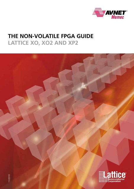
THE NON-VOLATILE FPGA GUIDE LATTIcE XO, XO2 AND XP2
THE NON-VOLATILE FPGA GUIDE LATTIcE XO, XO2 AND XP2
THE NON-VOLATILE FPGA GUIDE LATTIcE XO, XO2 AND XP2

You also want an ePaper? Increase the reach of your titles
YUMPU automatically turns print PDFs into web optimized ePapers that Google loves.
<strong>THE</strong> <strong>NON</strong>-<strong>VOLATILE</strong> <strong>FPGA</strong> <strong>GUIDE</strong><br />
<strong>LATTIcE</strong> <strong>XO</strong>, <strong>XO</strong>2 <strong>AND</strong> <strong>XP2</strong><br />
11/2010
MAcH<strong>XO</strong> FAMILY<br />
crossover Programmable Logic Devices<br />
The Mach<strong>XO</strong> family of non-volatile, infinitely<br />
reconfigurable Programmable Logic Devices (PLDs) is<br />
designed for applications traditionally implemented using<br />
CPLDs or low-capacity <strong>FPGA</strong>s. The Mach<strong>XO</strong> family combines<br />
an optimised Look-Up Table (LUT) fabric with Lattice’s ispXP<br />
technology to provide the high pin-to-pin performance<br />
and instant-on associated with CPLDs, with the flexibility of<br />
<strong>FPGA</strong>s, all in a low-cost device.<br />
The Mach<strong>XO</strong> family offers a high pin-to-logic ratio that is<br />
ideal for glue logic, bus bridging, bus interfacing, powerup<br />
control and control logic. In addition, Mach<strong>XO</strong> devices<br />
feature Lattice‘s exclusive sysCLOCK PLLs, sysMEM<br />
embedded memory blocks (EBRs) and high-performance I/Os.<br />
These features further facilitate the design of high-speed<br />
systems. Designs for Mach<strong>XO</strong> can easily be completed with<br />
Lattice‘s free ispLEVER ® Starter design software.<br />
Key Features and Benefits<br />
Non-Volatile, Infinitely Reconfigurable<br />
• Instant-on, powers up in less than 1 mS<br />
• Single-chip, no external configuration memory<br />
• Excellent design security, no bit stream to intercept<br />
2<br />
Performance to 3.5ns Pin-to-Pin<br />
TransFR Technology Allows Simple Field Upgrades<br />
Flexible LUT Architecture<br />
• 256 to 2280 LUT4s<br />
• 73 to 271 I/Os with extensive package options<br />
• Density migration supported<br />
Embedded and Distributed Memory<br />
• Up to 27.6 Kbits sysMEM Embedded Block RAM<br />
• Includes dedicated FIFO control logic<br />
• Up to 7.7 Kbits distributed RAM<br />
Flexible I/O Buffer<br />
• Programmable sysIO buffer supports wide range of<br />
interfaces:<br />
• LVCMOS 3.3/2.5/1.8/1.5/1.2<br />
• LVTTL<br />
• PCI*<br />
• LVDS*, Bus-LVDS*, LVPECL*, RSDS*<br />
sysCLOCK PLLs<br />
• Up to two analog PLLs per device<br />
• Clock multiply, divide and phase shifting<br />
Sleep Mode Reduces Standby Power to
MAcH<strong>XO</strong> Block Diagram<br />
sysClock PLLs for<br />
clock management<br />
sysMEM Embedded<br />
Block RAM (EBR)<br />
provides 9 kbit true dual port<br />
RAM at up to 275 MHz<br />
Programmable Function<br />
Unit (PFU) with RAM<br />
JTAG Port<br />
for configuration Flash<br />
and SRAM memory<br />
JTAG<br />
SysMEM Embedded Block RAM (EBR)<br />
Mach<strong>XO</strong>1200 and Mach<strong>XO</strong>2280 devices include flexible<br />
sysMEM EBR blocks. sysMEM EBR blocks provide on-chip<br />
memory resources to support a broad range of features.<br />
• Up to 27.6 K Bits sysMEM Embedded Block RAM (EBR)<br />
• 275 MHz Operation<br />
• Configurable Width and Depth<br />
• Single Port, Dual Port and Pseudo-Dual Port<br />
• Dedicated Logic for FIFO Control<br />
• Bus Size Matching<br />
• RAM Initialisation and User ROM Operation<br />
• Memory Cascading<br />
Mach<strong>XO</strong> devices bring together<br />
the best features of <strong>FPGA</strong>s and<br />
CPLDs ... low cost, outstanding<br />
pin-to-pin performance, and<br />
instant-on start-up. Plus, Mach<strong>XO</strong> devices are available in<br />
space-saving, RoHS-compliant packaging.<br />
Flash Memory<br />
sysMEM configuration<br />
Single Port Dual Port Pseudo-Dual Port FIFO<br />
8192 x 1 8192 x 1 8192 x 1 8192 x 1<br />
4096 x 2 4096 x 2 4096 x 2 4096 x 2<br />
2048 x 4 2048 x 4 2048 x 4 2048 x 4<br />
1024 x 9 1024 x 9 1024 x 9 1024 x 9<br />
512 x 18 512 x 18 512 x 18 512 x 18<br />
256 x 36 – 256 x 36 256 x 36<br />
Upgrade<br />
Flash<br />
FLASH<br />
(Configuration 2)<br />
Logic – SRAM<br />
(Configuration 1)<br />
Program Flash in background<br />
while logic functions<br />
On-chip Flash Memory offers<br />
instant-on start-up and security<br />
from bitstream snooping<br />
Flexible Routing optimised for<br />
speed, low-cost, and routability<br />
Programmable Function Unit<br />
without RAM (PFF)<br />
sysIO Buffers support LVCMOS /<br />
LVTTL, LVDS and PCI<br />
FLASH<br />
(Configuration 2)<br />
Upgrade<br />
SRAM<br />
Logic – SRAM<br />
(Configuration 2)<br />
JTAG commands control I/O & logic<br />
states while Flash is copied to SRAM<br />
– Device is operational in
MAcH<strong>XO</strong> FAMILY<br />
MachXo Device Selection Guide<br />
4<br />
Feature LcM<strong>XO</strong>256 LcM<strong>XO</strong>640 LcM<strong>XO</strong>1200 LcM<strong>XO</strong>2280<br />
LUTs 256 640 1200 2280<br />
Distributed RAM (Kbits) 2 6.1 6.4 7.7<br />
Embedded Block RAM – EBR (Kbits) – – 9.2 27.6<br />
Number of EBR Blocks – – 1 3<br />
V CC Voltage (V) Options 1.2 V or 1.8 / 2.5 / 3.3 V 1.2 V or 1.8 / 2.5 / 3.3 V 1.2 V or 1.8 / 2.5 / 3.3 V 1.2 V or 1.8 / 2.5 / 3.3 V<br />
Number of PLLs – – 1 2<br />
Number of I/O Banks 2 4 8 8<br />
Maximum Number of I/Os 78 159 211 271<br />
Maximum Number of LVDS Pairs* – – 27 33<br />
Packages & I/O combinations<br />
100-pin TQFP (14 x 14 mm)** 78 74 73 73<br />
144-pin TQFP (20 x 20 mm) 113 113 113<br />
100-ball csBGA (8 x 8 mm) 78 74<br />
132-ball csBGA (8 x 8 mm) 101 101 101<br />
256-ball caBGA (14 x 14 mm) 159 211 211<br />
256-ball ftBGA (17 x 17 mm) 159 211 211<br />
324-ball ftBGA (19 x 19 mm) 271<br />
* Number of LVDS outputs can be increased by emulating with external resistors. ** In the 100-pin TQFP package, designs can not migrate from LCM<strong>XO</strong>640 to 1200.<br />
LA-MachXo Automotive Family Selection Guide<br />
Feature LAM<strong>XO</strong>256E/c LAM<strong>XO</strong>640E/c LAM<strong>XO</strong>1200E LAM<strong>XO</strong>2280E<br />
LUTs 256 640 1200 2280<br />
Dist. RAM (Kbits) 2.0 6.0 6.25 7.5<br />
EBR SRAM (Kbits) 0 0 9.2 27.6<br />
Number of EBR SRAM Blocks (9 Kbits) 0 0 1 3<br />
V CC Voltage 1.2/1.8/2.5/3.3V 1.2/1.8/2.5/3.3V 1.2 1.2<br />
Number of PLLs 0 0 1 2<br />
Max. I/O 78 159 211 271<br />
Packages<br />
100-pin Lead-Free TQFP (14x14 mm) 78 74 73 73<br />
144-pin Lead-Free TQFP (20x20 mm) 113 113 113<br />
256-ball Lead-Free ftBGA (17x17 mm) 159 211 211<br />
324-ball Lead-Free ftBGA (19x19 mm) 271
MAcH<strong>XO</strong>2 FAMILY<br />
Optimised for consumer and System control<br />
Applications<br />
The Mach<strong>XO</strong>2 family of non-volatile infinitely reconfigurable<br />
Programmable Logic Devices (PLDs) is designed for low-power<br />
consumer applications such as smart phones, GPS devices<br />
and PDAs, as well as for system control applications found in<br />
telecommunications infrastructure, computing, industrial and<br />
medical equipment. Combining an optimized lookup table (LUT)<br />
architecture with 65-nm embedded Flash process technology,<br />
Mach<strong>XO</strong>2 devices provide a flexible “do-it-all” solution for designs.<br />
The Mach<strong>XO</strong>2 family offers system designers the benefits of<br />
increased system integration, improved system robustness and<br />
reduced static power consumption. In addition, the Mach<strong>XO</strong>2<br />
family includes hardened implementations of some of the most<br />
popular functions used in system control applications such as User<br />
Flash Memory (UFM), I 2 C, SPI and timer/counter. Thus, through the<br />
provision of these features, the Mach<strong>XO</strong>2 family offers customers a<br />
“do-it-all PLD”.<br />
Mach<strong>XO</strong>2 devices are available in three options: high performance<br />
(HC, HE) and ultra-low power (ZE).<br />
Mach<strong>XO</strong>2 control Application Example<br />
Control<br />
µP<br />
µP<br />
µP<br />
ASIC<br />
ASSP<br />
Custom, I 2 C<br />
SPI, LPC<br />
Mach<strong>XO</strong>2<br />
Bus<br />
Interface<br />
Status<br />
Registers<br />
Power<br />
Sequence<br />
& Reset<br />
LPC<br />
GPIO<br />
Delta<br />
Sigma/<br />
PWM<br />
Flash<br />
Controller<br />
Serial<br />
Bus<br />
Bridges<br />
I 2 C<br />
SPI<br />
1 2 3 4<br />
Flash<br />
5
MAcH<strong>XO</strong>2 FAMILY<br />
Three Product Options – More Flexibility<br />
Focus Option Regulator<br />
6<br />
Nominal<br />
Vcc (V)<br />
Internal<br />
Vcc (V)<br />
Low Power ZE – 1.2 1.2 60<br />
High HC 3.3, 2.5 1.2 150<br />
Performance HE – 1.2 1.2 150<br />
System<br />
Performance (MHz)<br />
Key Features and Benefits<br />
Large Number of I/Os<br />
• Up to 335 I/Os with broad range of package options<br />
Robust Architecture For Reliable Operation<br />
• Instant-on, powers up in less than 1 ms<br />
• Operate from a single 3.3 / 2.5 / 1.2 V supply<br />
• Input hysteresis allows operation in noisy environment<br />
Enhanced Security<br />
• Unique device Trace ID<br />
• One-time-programmability<br />
High Functional Integration For Cost Reduction<br />
• Densities ranging from 256 to 6864 LUTs<br />
• Up to 240 Kbits sysMEM Embedded Block RAM<br />
• Up to 54 Kbits Distributed RAM<br />
• Up to 256 Kbits of user Flash memory<br />
• Hardened I 2 C, SPI, timer/counter functions<br />
• Robust PLL with fractional division<br />
Flexible sysIO Buffer<br />
• Support for LVCMOS, LVTTL, LVDS, SSTL, HSTL interfaces<br />
• Hot socketing<br />
• On-chip differential termination<br />
• Programmable pull-up or pull-down mode<br />
Pre-Engineered Source Synchronous I/O<br />
• Dedicated gearing logic (7:1, 4:1, 8:1)<br />
• Generic DDR, DDRX2, DDRX4<br />
• Dedicated DDR/DDR2/LPDDR with DQS support<br />
Broad Device Offering<br />
• Commercial: 0 to 85 ºC (TJCOM)<br />
• Industrial: -40 to 100 ºC (TJIND)<br />
System Level Support<br />
• Reliable field updates with TransFR and Dual Boot<br />
• Security options include security bits, One Time<br />
Programmable (OTP) mode and unique device TraceID<br />
• IEEE 1532 Compliant In-System Programming<br />
• IEEE Standard 1149.1 boundary scan<br />
Ultra Low Power For Long Battery Life<br />
• As low as 19 μW static power<br />
• Manage power with power guard and power controller<br />
features
MAcH<strong>XO</strong>2<br />
ARcHITEcTURE<br />
Architecture Overview<br />
Mach<strong>XO</strong>2 PLDs are designed to offer an unprecedented mix<br />
of low cost, low power and high functionality in a single<br />
device. Through the use of 65-nm Flash technology and<br />
innovative design, Mach<strong>XO</strong>2 devices ultra low-power, small<br />
footprint, high system performance, a robust architecture,<br />
support for enhanced I/O features, on-chip UFM, hardened<br />
control functions and flexible security features.<br />
Mach<strong>XO</strong>2 Block Diagram<br />
sysCLOCK PLLs<br />
for frequency<br />
synthesis & clock<br />
alignment<br />
Programmable<br />
Function Units<br />
(PFUs) with RAM<br />
sysMEM Block<br />
9 Kbit Dual Port<br />
RAMs<br />
Advanced clocking Technology<br />
• Full featured PLL<br />
• Fractional division improves frequency synthesis<br />
• 10 to 400 MHz operation<br />
• On-chip oscillator with +/-5% accuracy over PVT and<br />
2 to 133 MHz operation<br />
Flash Memory<br />
sysMEM configuration Options<br />
Single<br />
Port<br />
Dynamic<br />
Phase<br />
Adjust<br />
Feedback<br />
Divider<br />
True Dual<br />
Port<br />
Embedded Functional Block<br />
offers hardened SPI, I 2 C, and<br />
timer / counter<br />
UFM (User Flash Memory)<br />
On-chip Flash Memory<br />
provides instant-on, high<br />
security & single chip solution<br />
sysIO Buffers<br />
support a wide range of interfaces<br />
including source synchronous I/Os.<br />
I/O logic supports 7:1 input gearing.<br />
Input<br />
Divider<br />
Fractional<br />
-N<br />
Synthesizer<br />
sysCLOCK PLL<br />
Phase<br />
Freq.<br />
Detect<br />
Pseudo-<br />
Dual Port<br />
VCO<br />
Output<br />
Divider<br />
Output<br />
Divider<br />
Output<br />
Divider<br />
Output<br />
Divider<br />
FIFO<br />
8192 x 1 8192 x 1 8192 x 1 8192 x 1<br />
4096 x 2 4096 x 2 4096 x 2 4096 x 2<br />
2048 x 4 2048 x 4 2048 x 4 2048 x 4<br />
1024 x 9 1024 x 9 1024 x 9 1024 x 9<br />
512 x 18 512 x 18<br />
Phase<br />
Adjust<br />
Edge<br />
Trim<br />
Phase<br />
Adjust<br />
Edge<br />
Trim<br />
Phase<br />
Adjust<br />
Edge<br />
Trim<br />
Phase<br />
Adjust<br />
Edge<br />
Trim<br />
7
MAcH<strong>XO</strong>2<br />
ARcHITEcTURE<br />
On-chip User Flash Memory<br />
sysIO Buffers Support<br />
• Programmable sysIO supports wide range of interfaces:<br />
• LVTTL, LVCMOS (3.3/2.5/1.8/1.5/1.2)<br />
• PCI*, LVDS*, Bus-LVDS, MLVDS<br />
• RSDS, LVPECL<br />
• SSTL 25/18, HSTL 18<br />
• Up to 256 Kbits<br />
• Input hysteresis<br />
• Hot socketing<br />
• On-chip differential termination*<br />
• Programmable pull-up, pull-down, bus keeper (I/O cell<br />
defaults to pull-down during power-up)<br />
• DDR registers in I/O cells<br />
• Dedicated gearing logic<br />
* Available on <strong>XO</strong>2-1200 and larger densities.<br />
8<br />
Read / Write from Fabric<br />
UFM EBR<br />
Logic<br />
Configuration<br />
FLASH<br />
JTAG / SPI / I 2 C<br />
Logic<br />
Configuration<br />
SRAM<br />
Mach<strong>XO</strong>2 Voltage Options<br />
1.2 V 3.3 / 2.5 V 1.2 V<br />
VCC VCCIO VCC VCCIO VCC VCCIO Mach<strong>XO</strong>2<br />
ZE<br />
Embedded function block<br />
Asymmetrical Banking<br />
Scheme Increases Flexibility<br />
Bank 3 Bank 4 Bank 5<br />
Mach<strong>XO</strong>2<br />
HC<br />
Mach<strong>XO</strong>2<br />
HE<br />
SPI I 2 C I 2 C Timer<br />
WISHBONE BUS<br />
Mach<strong>XO</strong>2 Fabric<br />
Bank 0<br />
Mach<strong>XO</strong>2<br />
Bank 2<br />
Bank 1<br />
Note: Mach<strong>XO</strong>2-256, 640 & 1200 LUT devices<br />
have four banks.
Easy, Reliable Field Updates<br />
Lattice’s Transparent Field Reconfiguration (TransFR)<br />
technology enables logic updates in the field without<br />
interrupting the operation of the system.<br />
Step 1<br />
Program Flash in<br />
background while<br />
logic functions<br />
Step 2<br />
Precisely control<br />
I/Os and initiate<br />
Flash to SRAM<br />
transfer through<br />
JTAG.<br />
Upgrade<br />
Flash<br />
FLASH<br />
(Configuration 2)<br />
Logic – SRAM<br />
(Configuration 1)<br />
FLASH<br />
(Configuration 2)<br />
Upgrade<br />
SRAM<br />
Logic – SRAM<br />
(Configuration 2)<br />
Dual Boot for Reliability<br />
Mach<strong>XO</strong>2 devices offer an additional level of reliability by<br />
supporting dual boot with external SPI Flash.<br />
Loads active configuration at power-up<br />
FLASH<br />
(Active Configuration)<br />
Read<br />
Data<br />
LOGIC SRAM<br />
Golden<br />
Configuration<br />
Control<br />
If active configuration fails, then the<br />
golden configuration is loaded<br />
SPI<br />
Configuration<br />
Memory<br />
Programming Options<br />
Mach<strong>XO</strong>2 devices offer several programming options,<br />
including: JTAG IEEE 1149.1/1532, I2C Slave, and SPI<br />
Master / Slave modes.<br />
Flexible Security Options<br />
Mach<strong>XO</strong>2 devices support<br />
optional security bits and a One-<br />
Time-Programmable (OTP) mode<br />
that prevents further erasure<br />
or programming of the Flash<br />
memory. A unique 64-bit device<br />
TraceID can be used for tracking<br />
purposes.<br />
Broad Range of Space-Saving<br />
Package Options<br />
Mach<strong>XO</strong>2 devices are available in a<br />
wide range of advanced halogenfree<br />
packages. Mach<strong>XO</strong>2 devices<br />
are designed to provide density<br />
migration within the same package.<br />
9
MAcH<strong>XO</strong>2<br />
ARcHITEcTURE<br />
Reference Design Portfolio<br />
Lattice offers an expanding portfolio of IP cores and reference<br />
designs targeted for system applications. Optimized for the<br />
Mach<strong>XO</strong>2 architecture, these include I2C, SPI, UART, PWM<br />
fan control, LCD controller, and LatticeMico8 microcontroller.<br />
The reference designs, source codes and documentation can<br />
be downloaded for free from the Lattice website. For more<br />
information, go to www.latticesemi.com/ip.<br />
Device Selection Guide<br />
Feature <strong>XO</strong>2-256 <strong>XO</strong>2-640 <strong>XO</strong>2-1200 <strong>XO</strong>2-2000 <strong>XO</strong>2-4000 <strong>XO</strong>2-7000<br />
LUTs 256 640 1280 2112 4320 6864<br />
Embedded RAM (Kbits) 0 18 64 74 92 240<br />
Distributed RAM (Kbits) 2 5 10 16 34 54<br />
UFM (Kbits) 0 24 64 80 96 256<br />
PLL 0 0 1 1 2 2<br />
Hardened Control Functions:<br />
I 2 C (2), SPI (1), Timer / Counter (1)<br />
Package I/O<br />
25 WLCSP (2.5 x 2.5 mm, 0.4 mm)* 18<br />
10<br />
<br />
36 WLCSP (3.1 x 3.1 mm, 0.4 mm)* 29<br />
64 μcBGA (4 x 4 mm, 0.4 mm) 45<br />
100 TQFP (14 x 14 mm, 0.5 mm) 56 79 80 80<br />
132 csBGA (8 x 8 mm, 0.5 mm) 56 80 105 105 105<br />
144 TQFP (20 x 20 mm, 0.5 mm) 108 112 115 115<br />
256 caBGA (14 x 14 mm, 0.8 mm) 207 207 207<br />
256 ftBGA (17 x 17 mm, 1.0 mm) 207 207 207<br />
332 caBGA (17 x 17 mm, 0.8 mm) 275 279<br />
484 fpBGA (23 x 23 mm, 1.0 mm) 279 335<br />
Typical Static Power<br />
ZE (μW) 19 33 70 98 153 230<br />
HC (mW) 4 7 13 18 32 48<br />
HE (mW) 2 3 5<br />
*Contact your Lattice sales representative for the support of WLCSP packages.
<strong>LATTIcE</strong><strong>XP2</strong> FAMILY<br />
FlexiFLASH: Instant-on, Secure, Single-chip <strong>FPGA</strong><br />
Lattice<strong>XP2</strong> devices combine a Look-up Table (LUT) based<br />
<strong>FPGA</strong> fabric with Flash non-volatile cells in an architecture<br />
referred to as flexiFLASH. The flexiFLASH approach<br />
provides a single chip solution with benefits such as<br />
instant-on operation, onchip storage featuring FlashBAK<br />
embedded block RAM backup, access to general-purpose<br />
Serial TAG memory and inherent design security. Lattice<strong>XP2</strong><br />
devices also support Live Update field reconfiguration with<br />
TransFRTM, 128-bit AES bitstream encryption and Dual Boot<br />
technologies.<br />
The Lattice<strong>XP2</strong> <strong>FPGA</strong> fabric utilizes an underlying<br />
LatticeECP2 architecture that was optimized from the<br />
outset with high performance and low cost in mind.<br />
Lattice<strong>XP2</strong> devices support 4-input LUT-based logic,<br />
distributed and embedded memory, Phase Locked Loops<br />
(PLLs), pre-engineered source synchronous I/O and enhanced<br />
sysDSPTM blocks.<br />
Lattice‘s ispLEVER ® design tool allows complex designs to<br />
be efficiently implemented using the Lattice<strong>XP2</strong> family of<br />
<strong>FPGA</strong>s. The ispLEVER tool is complemented by pre-designed<br />
IP (Intellectual Property) ispLeverCORE modules for the<br />
Lattice<strong>XP2</strong> family. By using these as standardized IP blocks,<br />
designers are free to concentrate on the unique aspects of<br />
their design, increasing their productivity.<br />
Key Features and Benefits<br />
• FlexiFLASH Architecture<br />
• Instant-on (1 mS), single chip integration<br />
• FlashBAK technology<br />
• General-purpose Serial TAG memory<br />
• Design security<br />
• Live Update Technology<br />
• TransFR technology – update logic configuration<br />
while equipment continues to operate<br />
• Dual Boot with external SPI Flash improves reliability<br />
• Secure updates with 128 bit AES bitstream encryption<br />
• Optimized <strong>FPGA</strong> Architecture<br />
• Densities from 5K to 40K 4-input Look-up Tables (LUTs)<br />
• Up to 885 Kbits sysMEM block RAM<br />
• Up to 83 Kbits distributed RAM<br />
• Low cost TQFP, PQFP and BGA packaging<br />
• High Performance sysDSP Block<br />
• Three to eight blocks with multiply and accumulate<br />
• 12 to 32 18x18 multipliers<br />
• Flexible sysIO Buffer Supports:<br />
• LVCMOS 3.3/2.5/1.8/1.5/1.2; LVTTL<br />
• SSTL 18 class I, II; SSTL 3/2 class I, II<br />
• HSTL15 class I; HSTL18 class I, II<br />
• PCI<br />
• LVDS, Bus-LVDS, LVPECL<br />
• Pre-engineered Source Synchronous Interfaces<br />
• DDR / DDR2 up to 200 MHz / 400 Mbps<br />
• 7:1 LVDS up to 600 Mbps<br />
• Generic up to 750 Mbps<br />
• Up to 4 sysCLOCK PLLs<br />
• Standby Power Reduced by 33%<br />
• System Level Support<br />
• SPI/JTAG interface for device programming<br />
• IEEE Standard 1149.1 Boundary Scan<br />
• Onboard oscillator for initialization & general use<br />
• Soft Error Detect (SED) logic<br />
• 1.2 V power supply core voltage<br />
11
<strong>LATTIcE</strong><strong>XP2</strong> FAMILY<br />
Lattice<strong>XP2</strong> Block Diagram<br />
12<br />
On-chip Oscillator<br />
sysIO Buffers support LVCMOS,<br />
HSTL, SSTL, LVDS and more<br />
sysMEM Embedded Block RAM<br />
(EBR) provides up to 885 Kbit with<br />
speeds up to 350 MHz.<br />
sysDSP Blocks include multiply and<br />
accumulate, up to 32 18x18 multipliers,<br />
and speeds up to 325 MHz.<br />
Programmable Function Unit<br />
(PFU) provide up to 40 K LUTs and<br />
speeds up to 350 MHz.<br />
Architecture Overview<br />
Lattice<strong>XP2</strong> <strong>FPGA</strong>s combine on-chip Flash memory with<br />
SRAM programmable LUTs and interconnect to provide<br />
an optimized low cost architecture that delivers high<br />
performance sysMEM embedded RAM blocks, distributed<br />
memory, sysCLOCK PLLs, DDR memory interface, sysIO<br />
buffers, and more.<br />
FLASH<br />
JTAG<br />
FLASH<br />
syscLOcK PLL Block Diagram<br />
Control<br />
Signals<br />
Clock<br />
Input<br />
Clock<br />
Feedback<br />
Reset<br />
Devider<br />
Devider<br />
Internal Feedback<br />
Phase<br />
Frequency<br />
Detector/<br />
Voltage<br />
Control<br />
Oscillator<br />
Pre-Engineered Source<br />
Synchronous I/O supports<br />
DDR/DDR2 & 7:1 LVDS.<br />
flexiFLASH architecture offers a secure,<br />
instant-on, single chip solution.<br />
JTAG and SPI Ports with Live<br />
Update technology.<br />
sysCLOCK Plls for clock<br />
management. Up to 4 per device.<br />
Devider<br />
Phase/<br />
Duty Cycle/<br />
Duty Trim<br />
Duty Trim<br />
Devider<br />
Lock Detect<br />
÷3<br />
Clock Outputs
sysIO Block Diagram<br />
<strong>FPGA</strong><br />
Fabric<br />
Phase<br />
Frequency<br />
Detector /<br />
Voltage<br />
Control<br />
Oscillator<br />
PFU Block Diagram<br />
Tri-State<br />
Register Block<br />
(2 Flip / Flops)<br />
Output<br />
Register Block<br />
(2 Flip / Flops)<br />
Input<br />
Register Block<br />
(5 Flip / Flops)<br />
DQS/Strobe Delay & Transition Detect<br />
From<br />
Routing<br />
LUT4<br />
LUT4<br />
LUT4<br />
LUT4<br />
LUT4<br />
LUT4<br />
LUT4<br />
LUT4<br />
LUT4<br />
LUT4<br />
LUT4<br />
LUT4<br />
LUT4<br />
Carry Chain<br />
Carry Chain<br />
Slice 3<br />
FF<br />
Slice 2<br />
FF<br />
FF<br />
FF<br />
FF<br />
Slice 1<br />
FF<br />
FF<br />
FF<br />
FF<br />
Slice 0<br />
FF<br />
FF<br />
FF<br />
FF<br />
To<br />
Routing<br />
sysDSP Block Diagram<br />
Adder/<br />
Multipliers Subtractor/<br />
Accumulator<br />
Summation<br />
Input<br />
Registers<br />
sysMEM EBR Primitives<br />
AD[12:0]<br />
DI[35:0]<br />
CLK<br />
CE<br />
RST<br />
WE<br />
CS[2:0]<br />
AD[12:0]<br />
CLK<br />
CE<br />
RST<br />
CS[2:0]<br />
Pipeline<br />
Registers<br />
+ - Σ<br />
+ - Σ<br />
+<br />
Output<br />
Registers<br />
Single Port RAM Dual Port RAM<br />
ADA[12:0]<br />
DIA[17:0]<br />
CLKA<br />
CEA<br />
EBR DO[35:0]<br />
EBR<br />
RSTA<br />
WEA<br />
CSA[2:0]<br />
DOA[17:0]<br />
ROM Pseudo Dual Port RAM<br />
ADW[12:0]<br />
DI[17:0]<br />
CLKW<br />
EBR DO[35:0] CEW<br />
WE<br />
RST<br />
CS[2:0]<br />
EBR<br />
ADB[13:0]<br />
DIB[17:0]<br />
CEB<br />
CLKB<br />
RSTB<br />
WEB<br />
CSB[2:0]<br />
DOB[17:0]<br />
ADR[13:0]<br />
DO[35:0]<br />
CER<br />
CLKR<br />
13
FLEXIFLASH: OVERVIEw<br />
14<br />
<strong>FPGA</strong><br />
Logic<br />
Flash Memory<br />
EBR Blocks<br />
Flash<br />
SPI /<br />
JTAG<br />
Port<br />
FlashBAK technology allows storage of multipl data types:<br />
error codes, data tables, and microprocessor code.<br />
EBR Blocks<br />
SRAM<br />
Configuration Bits<br />
EBR Blocks<br />
Decryption & Device Lock<br />
This approach provides a single chip solution, instant-on (1 mS),<br />
FlashBAK EBR,TAG memory and design security.<br />
FlashBAK Technology<br />
Write to Flash during programming.<br />
Write from Flash to EBRs during<br />
configuration. Write from EBR to<br />
Flash on user command.<br />
Make infinite reads & writes to<br />
EBR @ up to 350 MHz.<br />
TAG<br />
Memory<br />
Flash Memory<br />
JTAG<br />
<strong>FPGA</strong><br />
Logic<br />
SPI &<br />
JTAG<br />
Serial TAG Memory<br />
Sequential<br />
Address Counter<br />
Fast parallel data transfer for<br />
instant-on.<br />
FLASH for single chip solution.<br />
FlashBAK for sysMEM EBR storage.<br />
Device lock for design security.<br />
TDI TDO<br />
Data Shift<br />
Register (Nx8)<br />
Flash<br />
Memory<br />
Array<br />
JTAG<br />
<strong>FPGA</strong><br />
Logic<br />
Use Serial TAG Memory to store items such as Board ID, calibration<br />
data, and manufacturing information.
LIVE UPDATE – FLEXILBLE, RENTABLE<br />
<strong>AND</strong> SEcURE UPDATES<br />
Live Update Technology<br />
Field logic update continues to increase in importance in<br />
a wide variety of applications due to the unprecedented<br />
flexibility that it provides designers to fix bugs, respond to<br />
changing standards, upgrade equipment and add additional<br />
services. Lattice‘s Live Update technology allow logic to be<br />
reliably updated in the field without interrupting system<br />
operation<br />
Lattice<strong>XP2</strong><br />
Flash<br />
(Configuration 2)<br />
Logic-SRAM<br />
(Configuration 1)<br />
Lattice<strong>XP2</strong><br />
Flash<br />
(Configuration 2)<br />
Logic-SRAM<br />
(Configuration 1)<br />
Step 1<br />
While the device is<br />
operating, Load New<br />
Configuration (2) to<br />
Configuration Memory<br />
Step 2<br />
Lock the I/Os in the Desired<br />
States<br />
Step 3<br />
Transfer New Configuration<br />
to Logic<br />
Step 4<br />
Lattice<strong>XP2</strong> <strong>FPGA</strong> Regains<br />
Control of I/Os<br />
SPI Configuration<br />
Memory<br />
Read Data<br />
Lattice<strong>XP2</strong><br />
Flash<br />
(Active Config)<br />
Backup<br />
(Golden)<br />
Configuration Logic-SRAM<br />
Control<br />
Minimize Field Calls Add Services Features Respond to Changeing Standards<br />
Customer Site Head Office Customer Site<br />
Transfer technology Dual boot for reliable update 128-bit AES bitstream encryption<br />
If error detected in active configuration<br />
then backup (golden) configuration is<br />
loaded from SPI Flash.<br />
128 Bit AES<br />
Encrypted Bitstream<br />
Decryption<br />
Engine<br />
128-Bit<br />
Key<br />
Lattice<strong>XP2</strong><br />
Flash<br />
(Configuration)<br />
Logic-SRAM<br />
Design specific key stored in<br />
on-chip Flash.<br />
<strong>XP2</strong> Device Selection Guide<br />
Feature LF<strong>XP2</strong>-5 LF<strong>XP2</strong>-8 LF<strong>XP2</strong>-17 LF<strong>XP2</strong>-30 LF<strong>XP2</strong>-40<br />
LUTs (K) 5 8 17 29 40<br />
sysMEM EBR RAM Blocks 9 12 15 21 48<br />
Embedded Memory (Kbits) 166 221 276 387 885<br />
Distributed Memory (Kbits) 10 18 35 56 83<br />
sysDSP Blocks 3 4 5 7 8<br />
Number of 18x18 Multipliers 12 16 20 28 32<br />
Number of PLLs 2 2 4 4 4<br />
V Voltage (V) CC<br />
Packages & I/O combinations<br />
1.2 1.2 1.2 1.2 1.2<br />
132-ball csBGA (8 x 8 mm) 86 86<br />
144-pin TQFP (20 x 20 mm) 100 100<br />
208-pin PQFP (28 x 28 mm) 146 146 146<br />
256-ball ftBGA (17 x 17 mm) 172 201 201 201<br />
484-ball fpBGA (23 x 23 mm) 358 363 363<br />
672-ball fpBGA (27 x 27 mm) 472 540<br />
15
DEVELOPMENT HARDwARE<br />
MAcH<strong>XO</strong> USB connection Starter Kit<br />
MACH<strong>XO</strong> USB connection Starter Kit is a complete hardware<br />
kit, including everything required to program, evaluate and<br />
de-bug a design for the Lattice Mach<strong>XO</strong> architecture.<br />
Product contents<br />
• MACH<strong>XO</strong> USB Kit featuring:<br />
• Mach<strong>XO</strong> device: LCM<strong>XO</strong>640C-3TN144C<br />
• Power via JTAG and USB<br />
• Step-down-conversion for 3.3V<br />
• 24 MHz oscillator<br />
• 8 LEDs<br />
• Power LED<br />
• 4-input DIP switch<br />
• USB-A connector incl. USB cable (A-A)<br />
• Data-CD and Lattice Starter-SW<br />
• Access to all device I/O<br />
• Download via USB-connection<br />
Ordering Information<br />
Part Number: HWD-<strong>XO</strong>-USB<br />
16<br />
MAcH<strong>XO</strong> Development Kits<br />
The Mach<strong>XO</strong> Mini Development Kit is an easy to use, lowcost<br />
platform to accelerate the evaluation of Mach<strong>XO</strong> PLDs.<br />
The kit features the Mach<strong>XO</strong> LCM<strong>XO</strong>2280 device, 2 Mbit SPI<br />
Flash and 1 Mbit SRAM memory, a temperature sensor, an<br />
expansion header for I 2 C and SPI interfaces, and several LEDs<br />
and user switches.<br />
The Mach<strong>XO</strong> Control Development Kit is a platform for<br />
rapidly prototyping system control designs using Mach<strong>XO</strong><br />
PLDs. The kit features the Mach<strong>XO</strong> LCM<strong>XO</strong>2280 device,<br />
Power Manager II ispPAC-POWR1014A, 2 Mbit SPI Flash and<br />
1 Mbit SRAM memory, a temperature sensor, an expansion<br />
header for I 2 C and SPI interfaces, and several LEDs and user<br />
switches.<br />
Ordering Information<br />
Part Number:<br />
LCM<strong>XO</strong>2280C-C-EVN<br />
LCM<strong>XO</strong>2280C-M-EVN
MAcH<strong>XO</strong>2<br />
Evaluation and Development Kits<br />
Mach<strong>XO</strong>2 Control<br />
Development Board<br />
Mach<strong>XO</strong>2 Pico<br />
Development Board<br />
Lattice offers a number of evaluation and development<br />
boards that provide a complete and easy-to-use platform<br />
to evaluate the performance of the Mach<strong>XO</strong>2, or aid in the<br />
development of custom designs. For more information, go<br />
to www.latticesemi.com/products/developmenthardware.<br />
The following devices are available:<br />
• Mach<strong>XO</strong> 640c<br />
• Mach<strong>XO</strong>1200c<br />
• Mach<strong>XO</strong>2280c<br />
and<br />
• XP3c<br />
• XP6c<br />
• <strong>XP2</strong>-17E<br />
• All devices in TQFP144<br />
• 25 MHz oscillator<br />
• 5 to 20 V external power supply<br />
• 2 V 5 lin. voltage regulator for LVDS<br />
• Power-LED<br />
• JTAG connector 10 pol and 8 pol<br />
• 8 LEDs<br />
• Dimensions: 83 x 61 mm<br />
Ordering information<br />
Part Number:<br />
LCM<strong>XO</strong>640C-eval-demo<br />
LCM<strong>XO</strong>1200C-eval-demo<br />
LCM<strong>XO</strong>2280C-eval-demo<br />
LFXP3C-eval-demo<br />
LFXP6C-eval-demoboard<br />
HWD<strong>XP2</strong>17EROHS<br />
17
DEVELOPMENT HARDwARE<br />
<strong>LATTIcE</strong><strong>XP2</strong> Advanced Evaluation Board<br />
The Lattice<strong>XP2</strong> Advanced Evaluation Board is a flexible<br />
platform designed to help you quickly evaluate the<br />
features and performance of the Lattice<strong>XP2</strong> <strong>FPGA</strong>, or aid in<br />
development of custom designs.<br />
Product contents<br />
Lattice<strong>XP2</strong> Advanced Evaluation Board featuring<br />
• Lattice<strong>XP2</strong>-17 <strong>FPGA</strong> in 484fpBGA package (LF<strong>XP2</strong>-17E-<br />
18<br />
4F484C)<br />
• DDR2 SDRAM SO-DIMM socket (32-bit)<br />
• Tri-speed Ethernet PHY (10/100/1G) / RJ45.<br />
• PCI 32-bit edge<br />
• LVDS Video Tx/Rx (via MDR-26 connectors)<br />
• PS/2 I/O<br />
• Compact Flash connector<br />
• SMAs for clock and general purpose I/O<br />
• A/D converter (ADS7842), D/A converter (DAC7617)<br />
• USB host/controller<br />
• Built-in USB download capability (includes Mach<strong>XO</strong> device)<br />
• RS-232 connector (female)<br />
• on-board oscillator (dip socket)<br />
• SPI flash memory for alternate configuration<br />
• LCD connector<br />
• 4 push-button switches, 8-bit switch<br />
• 7-segment LED, 8 general purpose LEDs<br />
• PAC1220AT8 for on-board power control<br />
Ordering Information<br />
Part Number: LF<strong>XP2</strong>-17E-H-EV<br />
<strong>LATTIcE</strong><strong>XP2</strong> Standard Evaluation Board<br />
The Lattice<strong>XP2</strong> Standard Evaluation Board is a flexible<br />
platform designed to help you quickly evaluate the<br />
features and performance of the Lattice<strong>XP2</strong> <strong>FPGA</strong>, or aid in<br />
development of custom designs.<br />
Product contents<br />
Lattice<strong>XP2</strong> Standard Evaluation Board featuring<br />
• Lattice<strong>XP2</strong>-17 <strong>FPGA</strong> in 484fpBGA package (LF<strong>XP2</strong>-17E-<br />
4F484C)<br />
• On-board Asynch SRAM memory (256Kx32 providing<br />
1Mbyte)<br />
• A/D converter (ADS7842), D/A converter (DAC7617)<br />
• 10K digital POT<br />
• RS232 DB9 „female“ connector<br />
• Compact Flash connector<br />
• 8-bit switch, 4 push-button switches<br />
• 7-segment LED, 8 general purpose LEDs<br />
• Built-in USB download capability (includes Mach<strong>XO</strong> device)<br />
• Selectable I/O voltage<br />
• SMA connectors for clock and general purpose I/O<br />
• PAC607 power manager<br />
• on-board oscillator (dip socket)<br />
• Proto/test area<br />
• SPI flash memory for alternate configuration<br />
• Power via Bellnix DC power control modules<br />
• LCD connector<br />
Ordering Information<br />
Part Number: LF<strong>XP2</strong>-17E-L-EV
PAcKAGE OFFERING<br />
<strong>THE</strong> <strong>NON</strong> <strong>VOLATILE</strong> TEcHNOLOGY<br />
Packages shown actual size. All dimensions refer to package body size.<br />
64-BALL<br />
ucBGA<br />
4 x 4 mm<br />
0.4 mm pitch<br />
LAM<strong>XO</strong> XXXX X –<br />
■ Device Family<br />
LA-Mach<strong>XO</strong><br />
Automotive<br />
Crossover PLD<br />
■ Logic Capacity<br />
256 LUTs = 256<br />
640 LUTs = 640<br />
1200 LUTs = 1200<br />
2280 LUTs = 2280<br />
■ Supply Voltage<br />
C = 1.8 V / 2.5 V / 3.3 V<br />
E = 1.2 V<br />
256-BALL<br />
caBGA<br />
8 x 8 mm<br />
14 x 14 mm<br />
14 x 14 mm<br />
17 x 17 mm<br />
0.5 mm pitch 0.5 mm pitch (100 TQFP) 0.8 mm pitch h 1.0 mm pitchh<br />
LA-MACH<strong>XO</strong> Automotive<br />
X XXXXXX X<br />
■ Speed<br />
3 = -3 Speed Grade<br />
■ Package<br />
TN100 = 100-pin Lead-Free TQFP<br />
TN144 = 144-pin Lead-Free TQFP<br />
FTN256 = 256-ball Lead-Free ftBGA<br />
FTN324 = 324-ball Lead-Free ftBGA<br />
■ Grade<br />
E = Automotive<br />
LATTICE<strong>XP2</strong><br />
LF<strong>XP2</strong> XX E – X XXXXX X<br />
■ Device Family<br />
Lattice<strong>XP2</strong><br />
■ Logic Capacity<br />
5 = 5 K LUTs<br />
8 = 8 K LUTs<br />
17 = 17 K LUTs<br />
30 = 30 K LUTs<br />
40 = 40 K LUTs<br />
■ Supply Voltage<br />
E = 1.2 V<br />
■ Speed<br />
5 = Slowest<br />
6<br />
7 = Fastest<br />
Only Mach<strong>XO</strong>256C(E), Mach<strong>XO</strong>640C(E),Mach<strong>XO</strong>1200E<br />
and Mach<strong>XO</strong>2280E are available for Automotive. LF<strong>XP2</strong> - 5E / 8E / 17E also available for Automotive Speedgrade.<br />
MACH<strong>XO</strong><br />
LCM<strong>XO</strong> XXXX X – X XXXXXX X<br />
■ Device Family<br />
Mach<strong>XO</strong> PLD<br />
■ Logic Capacity<br />
256 LUTs = 256<br />
640 LUTs = 640<br />
1200 LUTs = 1200<br />
2280 LUTs = 2280<br />
■ Supply Voltage<br />
C = 1.8 V / 2.5 V / 3.3 V<br />
E = 1.2 V<br />
■ Speed<br />
3 = Slowest<br />
4<br />
5 = Fastest<br />
■ Grade<br />
C = Commercial<br />
I = Industrial<br />
100-/132-BALL<br />
csBGA<br />
Ordering information<br />
■ Package<br />
T100 = 100-pin TQFP<br />
T144 = 144-pin TQFP<br />
M100 = 100-pin csBGA<br />
M132 = 132-ball csBGA<br />
B256 = 256-ball caBGA<br />
FT256 = 256-ball ftBGA<br />
FT324 = 324-ball ftBGA<br />
100-PIN<br />
TQFP<br />
T100 = 100-pin Lead-Free TQFP<br />
T144 = 144-pin Lead-Free TQFP<br />
M100 = 100-pin Lead-Free csBGA<br />
M132 = 132-ball Lead-Free csBGA<br />
BN256 = 256-ball Lead-Free caBGA<br />
FT256 = 256-ball Lead-Free ftBGA<br />
FT324 = 324-ball Lead-Free ftBGA<br />
MACH<strong>XO</strong>2<br />
LCM<strong>XO</strong>2 – XXXXX X X – X XXXXXX X<br />
■ Device Family<br />
Mach<strong>XO</strong>2 PLD<br />
■ Logic Capacity<br />
256 = 256 LUTs<br />
640 = 640 LUTs<br />
1200 = 1280 LUTs<br />
2000 = 2112 LUTs<br />
4000 = 4320 LUTs<br />
7000 = 6864 LUTs<br />
■ Power/Performance<br />
Z = Low Power<br />
H = High Performance<br />
■ Supply Voltage<br />
C = 2.5 V / 3.3 V<br />
E = 1.2 V<br />
■ Grade<br />
C = Commercial<br />
I = Industrial<br />
■ Package<br />
M132 = 132-ball csBGA<br />
FT256 = 256-ball ftBGA<br />
F484 = 484-ball fpBGA<br />
F672 = 672-ball fpBGA<br />
MN132 = 132-ball Lead-Free csBGA<br />
TN144 = 144-pin Lead-Free TQFP<br />
QN208 = 208-pin Lead-Free PQFP<br />
FTN256 = 256-ball Lead-Free ftBGA<br />
FN484 = 484-ball Lead-Free fpBGA<br />
FN672 = 672-ball Lead-Free fpBGA<br />
■ Grade<br />
C = Commercial<br />
I = Industrial<br />
■ Speed<br />
1 = Slowest<br />
2<br />
3 = Fastest<br />
4 = Slowest<br />
5<br />
6 = Fastest<br />
Low Power<br />
High Performance<br />
256-BALL<br />
ftBGA<br />
■ Package<br />
TG100 = 100-pin Halogen-Free TQFP<br />
TG144 = 144-pin Halogen-Free TQFP<br />
UMG64 = 64-ball Halogen-Free ucBGA<br />
(0.4 mm Pitch)<br />
MG132 = 132-ball Halogen-Free csBGA<br />
(0.8 mm Pitch)<br />
BG256 = 256-ball Halogen-Free caBGA<br />
(0.8 mm Pitch)<br />
FTG256 = 256-ball Halogen-Free ftBGA<br />
(1.0 mm Pitch)<br />
BG437 = 437-ball Halogen-Free caBGA<br />
FG484 = 484-ball Halogen-Free fpBGA<br />
(1.0 mm Pitch)<br />
144-PIN<br />
TQFP<br />
20 x 20 mm<br />
0.5 mm pitch<br />
484-BALL fpBGA<br />
23 x 23 mm<br />
1.0 mm pitch<br />
672-BALL<br />
fpBGA<br />
27 x 27 mm<br />
1.0 mm pitch<br />
208-PIN<br />
PQFP<br />
28 x 28 mm<br />
0.5 mm pitch<br />
332-Ball ll<br />
caBGA<br />
17 x 17 mm<br />
0.8 mm pitch h<br />
19
LOcATIONS<br />
AUSTRIA<br />
Avnet Memec<br />
(Avnet EMG Elektronische Bauelemente GmbH)<br />
Schönbrunner Str. 297 - 307 · A-1120 Vienna<br />
Phone +43 1 86642 500<br />
Fax +43 1 86642 550<br />
vienna@avnet-memec.eu<br />
BELGIUM<br />
Avnet Memec (Avnet Europe Comm. VA)<br />
Maaltecenter Blok G · Derbystraat 299 · B-9051 Gent<br />
Phone +32 9 243 70 70<br />
Fax +32 9 243 70 79<br />
gent@avnet-memec.eu<br />
czEcH REP, cROATIA, HUNGARY, SERBIA, SLOVAKIA,<br />
SLOVENIA<br />
Avnet Memec<br />
(Avnet EMG Elektronische Bauelemente GmbH)<br />
Schönbrunner Str. 297–307 · A-1120 Vienna<br />
Phone +43 1 86642 590<br />
Fax +43 1 86642 551<br />
vienna@avnet-memec.eu<br />
DENMARK<br />
Avnet Memec (Avnet Nortec A/S)<br />
Ellekær 9 · DK-2730 Herlev<br />
Phone +45 43 22 80 30<br />
Fax +45 43 22 80 31<br />
herlev@avnet-memec.eu<br />
FINL<strong>AND</strong>, ESTONIA<br />
Avnet Memec (Avnet Nortec Oy)<br />
Pihatörmä 1 B · FIN-02240 Espoo<br />
Phone +358 207 499 250<br />
Fax +358 207 499 255<br />
espoo@avnet-memec.eu<br />
FRANcE<br />
Avnet Memec (Avnet EMG France SA)<br />
6/8, Rue Ambroise Croizat - ZAE Les Glaises<br />
F-91127 Palaiseau Cedex<br />
Phone +33 1 64 47 90 80<br />
Fax +33 1 64 47 90 99<br />
paris@avnet-memec.eu<br />
Avnet Memec (Avnet EMG France SA)<br />
33, Rue du Docteur G. Levy<br />
Parc Club du moulin à Vent<br />
Bâtiment 40 · F-69693 Venissieux<br />
Phone +33 4 72 14 84 00<br />
Fax +33 4 72 14 10 03<br />
lyon@avnet-memec.eu<br />
Avnet Memec (Avnet EMG France SA)<br />
Espace Vilaine - 29, Avenue des Peupliers<br />
F-35510 Cesson Sévigné<br />
Phone +33 2 99 83 60 60<br />
Fax +33 2 99 83 60 69<br />
rennes@avnet-memec.eu<br />
Avnet Memec (Avnet EMG France SA)<br />
Parc de la Plaine - 35<br />
Avenue Marcel Dassault - BP5867<br />
F-31506 Toulouse Cedex<br />
Phone +33 5 62 47 47 70<br />
Fax +33 5 62 47 47 66<br />
toulouse@avnet-memec.eu<br />
Avnet Memec (Avnet EMG France SA)<br />
Parc de l‘Innovation Technologique<br />
1, Rue Gruninger<br />
F-67400 Illkirch-Graffenstaden<br />
Phone +33 3 88 39 69 03<br />
strasbourg@avnet-memec.eu<br />
GERMANY<br />
Avnet Memec (Avnet EMG GmbH)<br />
Wilhelmstraße 1 · D-59439 Holzwickede<br />
Phone +49 2301 919-0<br />
Fax +49 2301 919 200<br />
holzwickede@avnet-memec.eu<br />
Avnet Memec (Avnet EMG GmbH)<br />
Gutenbergstraße 15 · D-70771 Leinfelden-Echterdingen<br />
Phone +49 711 782 60 03<br />
Fax +49 711 782 60 555<br />
stuttgart@avnet-memec.eu<br />
Avnet Memec (Avnet EMG GmbH)<br />
Gruber Straße 60c · D-85586 Poing<br />
Phone +49 8121 775-0<br />
Fax +49 8121 775 594<br />
poing@avnet-memec.eu<br />
Avnet Memec Direct (Avnet EMG GmbH)<br />
Gruber Straße 60c · D-85586 Poing<br />
Phone +49 8121 775-190 (West/East)<br />
Phone +49 8121 775-191 (South)<br />
Phone +49 8121 775-192 (North)<br />
Fax +49 8121 775 591<br />
direct@avnet-memec.eu<br />
GREEcE<br />
Avnet Memec<br />
Anaxagora 1 Tavros · GR-17778 Athens<br />
Phone +30 22910-55831<br />
Fax +30 22910-54847<br />
greece@avnet-memec.eu<br />
ITALY<br />
Avnet Memec (Avnet EMG Italy SRL)<br />
Via Manzoni, 44 · I-20095 Cusano Milanino (MI)<br />
Phone + 39 02 66092 1<br />
Fax + 39 02 66092 496<br />
milan@avnet-memec.eu<br />
Avnet Memec (Avnet EMG Italy SRL)<br />
Viale dell’ Industria, 23 · I-35129 Padova<br />
Phone +39 049 78 18 116<br />
Fax +39 049 77 30 36<br />
padova@avnet-memec.eu<br />
NE<strong>THE</strong>RL<strong>AND</strong>S<br />
Avnet Memec (Avnet B.V.)<br />
Takkebijsters 2 · NL-4817BL Breda<br />
Phone +31 76 5722800<br />
Fax +31 76 5722808<br />
breda@avnet-memec.eu<br />
NORwAY<br />
Avnet Memec (Avnet Nortec AS)<br />
Ryensvingen 3B · Pb 101 Manglerud · N-0680 Oslo<br />
Phone +47 66 77 97 00<br />
Fax +47 66 77 97 01<br />
oslo@avnet-memec.eu<br />
POL<strong>AND</strong>, ROMANIA, BULGARIA, LATVIA,<br />
LITHUANIA<br />
Avnet Memec (Avnet EM Sp. z o.o.)<br />
ul. Staromiejska 7 · PL-40-013 Katowice<br />
Phone +48 32 337 56 20<br />
Fax +48 32 337 56 20 ext. 25<br />
katowice@avnet-memec.eu<br />
PORTUGAL<br />
Avnet Memec<br />
Tower Plaza · Rotunda Edgar Cardoso, 23 - 14 andar, Sala E<br />
P-4400-676 Vila Nova de Gaia<br />
Phone +351 22 377 95 02<br />
Fax +351 22 377 95 03<br />
porto@avnet-memec.eu<br />
RUSSIA, UKRAINE, BELARUS<br />
Avnet Memec<br />
Korovinskoye Chausse 10, Building 2, Office 26<br />
RUS-127486 Moscow<br />
Phone +7 495 937 87 08<br />
Fax +7 495 937 12 63<br />
moscow@avnet-memec.eu<br />
SPAIN<br />
Avnet Memec (Avnet Iberia SA)<br />
C/Chile, 10 - ofic. 222 - Edificio Madrid 92<br />
E-28290 Las Matas (Madrid)<br />
Phone +34 91 372 71 19<br />
Fax +34 91 372 72 13<br />
madrid@avnet-memec.eu<br />
Avnet Memec (Avnet Iberia SA)<br />
C/ Mallorca · 1-23. 2ª plta. 1A.<br />
E-08014 Barcelona<br />
Phone: +34 93 327 85 43<br />
Fax: +34 93 425 05 44<br />
barcelona@avnet-memec.eu<br />
Avnet Memec (Avnet Iberia SA)<br />
Plaza Zabalgane · 12. Bajo Izqda.<br />
E-48960 Galdacano. Vizcaya.<br />
Phone: +34 944 57 27 77<br />
Fax: +34 944 56 88 55<br />
bilbao@avnet-memec.eu<br />
SwEDEN<br />
Avnet Memec (Avnet Nortec AB)<br />
Esplanaden 3D · S-172 67 Sundbyberg<br />
Phone +46 8 587 46 300<br />
Fax +46 8 587 46 301<br />
sundbyberg@avnet-memec.eu<br />
SwITzERL<strong>AND</strong><br />
Avnet Memec (Avnet EMG AG)<br />
Gaswerkstr. 32 · CH-4900 Langenthal<br />
Phone +41 62 919 55 55<br />
Fax +41 62 919 55 00<br />
langenthal@avnet-memec.eu<br />
TURKEY<br />
Avnet Memec<br />
19 Mayıs Mah. Sümer Sok.<br />
Sümko Sitesi L2 Kozal Residence D:8<br />
TR-Erenköy, Istanbul<br />
Phone +90 21 63 72 64 72<br />
Fax +90 21 63 72 66 33<br />
istanbul@avnet-memec.eu<br />
UK & IREL<strong>AND</strong><br />
Avnet Memec (Avnet EMG Ltd.)<br />
Suite 4, First Floor · Oxford House · Oxford Road Thame<br />
Oxfordshire OX9 2AH, UK<br />
Phone +44 1844 263600<br />
Fax +44 1844 263601<br />
thame@avnet-memec.eu<br />
This document provides a brief overview only, no binding offers are<br />
intended. Avnet disclaims all representations, warranties and liabilities<br />
under any theory with respect to the product information, including any<br />
implied warranties of merchantability, fitness for a particular purpose, title<br />
and/or non-infringement, specifications, use, legal compliance or other<br />
requirements. Product information is obtained by Avnet from its suppliers or<br />
other sources deemed reliable and is provided by Avnet on an ‘AS IS’ basis.<br />
No guarantees as to the accuracy or completeness of any information are<br />
made. All information is subject to change, modifications and amendments<br />
without notice.<br />
www.avnet-memec.eu