Uncooled microbolometer detector: recent developments at ULIS
Uncooled microbolometer detector: recent developments at ULIS
Uncooled microbolometer detector: recent developments at ULIS

Create successful ePaper yourself
Turn your PDF publications into a flip-book with our unique Google optimized e-Paper software.
OPTO-ELECTRONICS REVIEW 14(1), 25–32<br />
<strong>Uncooled</strong> <strong>microbolometer</strong> <strong>detector</strong>: <strong>recent</strong> <strong>developments</strong> <strong>at</strong> <strong>ULIS</strong><br />
J.L. TISSOT * , C. TROUILLEAU, B. FIEQUE, A. CRASTES, and O. LEGRAS<br />
<strong>ULIS</strong>, BP 27 – 38113 Veurey-Voroize, France<br />
<strong>Uncooled</strong> infrared focal plane arrays are being developed for a wide range of thermal imaging applic<strong>at</strong>ions. Fire-fighting,<br />
predictive maintenance, process control and thermography are a few of the industrial applic<strong>at</strong>ions which could take benefit<br />
from uncooled infrared <strong>detector</strong>. Therefore, to answer these markets, a 35-µm pixel-pitch uncooled IR <strong>detector</strong> technology<br />
has been developed enabling high performance 160´120 and 384´288 arrays production. Besides a wide-band version from<br />
uncooled 320´240/45 µm array has been also developed in order to address process control and more precisely industrial<br />
furnaces control. The <strong>ULIS</strong> amorphous silicon technology is well adapted to manufacture low cost <strong>detector</strong> in mass production.<br />
After some brief <strong>microbolometer</strong> technological background, we present the characteriz<strong>at</strong>ion of 35 µm pixel-pitch <strong>detector</strong><br />
as well as the wide-band 320´240 infrared focal plane arrays with a pixel pitch of 45 µm.<br />
Keywords: uncooled IRFPA, 2D array, MWIR, LWIR, <strong>microbolometer</strong>, amorphous silicon.<br />
1. Introduction<br />
<strong>Uncooled</strong> infrared <strong>detector</strong>s are now available for various<br />
applic<strong>at</strong>ions. Their simple oper<strong>at</strong>ing conditions are similar<br />
to those of digital CMOS active pixel sensor (APS) used in<br />
some digital cameras. They have already shown their potentiality<br />
to fulfil many commercial and military applic<strong>at</strong>ions.<br />
One of the key parameters is the low cost achievable<br />
with uncooled <strong>detector</strong>s compared to cooled quantum <strong>detector</strong>s.<br />
Cooled <strong>detector</strong>s are designed for high performance<br />
systems and uncooled <strong>detector</strong>s are designed for<br />
low cost systems and mass production.<br />
This paper describes the advantages of the amorphous<br />
silicon technology, the characteriz<strong>at</strong>ion of 35-µm pixelpitch<br />
<strong>detector</strong>s and the characteriz<strong>at</strong>ion of wide-band<br />
320´240 uncooled <strong>detector</strong>s. Some mass production results<br />
and a short present<strong>at</strong>ion of the next bolometer gener<strong>at</strong>ion<br />
conclude the discussion.<br />
2. Background<br />
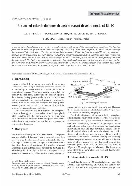
The bolometer is composed of a thermometer [1] integr<strong>at</strong>ed<br />
on a micro-bridge. This micro-bridge is supported by two legs<br />
anchored over the silicon substr<strong>at</strong>e by metal studs. This micro-bridge<br />
is built on a sacrificial layer which is removed in a<br />
final step. The micro-bridge is only 0.1 µm thick of doped<br />
amorphous silicon and the distance between the ROIC and the<br />
micro-bridge is 2.5 µm (Fig. 1). This vacuum gap works as a<br />
quarter wavelength cavity, which sets the <strong>detector</strong> spectral re-<br />
* e-mail: jl.tissot@ulis-ir.com<br />
The paper presented there appears in Infrared Photoelectronics,<br />
edited by Antoni Rogalski, Eustace L. Dereniak, Fiodor F. Sizov,<br />
Proc. SPIE Vol. 5957, 59570M (2005).<br />
Infrared Photoelectronics<br />
Fig. 1. Bolometer pixel structure.<br />
sponse maximum <strong>at</strong> a wavelength close to 10 µm. However,<br />
the measured response is still substantial in the 3–5 µm range<br />
as shown in the following paragraphs.<br />
Besides its silicon technology comp<strong>at</strong>ibility, amorphous<br />
silicon presents many other advantages. First, it enables the<br />
manufacturing of very thin suspended membranes (1000 )<br />
combined with short leg lengths resulting in high fill factor<br />
and high mechanical strength structures th<strong>at</strong> could sustain<br />
high vibr<strong>at</strong>ion r<strong>at</strong>es and high mechanical shocks. This reduced<br />
mechanical susceptibility to vibr<strong>at</strong>ion or shock solicit<strong>at</strong>ion<br />
is obviously important for many military as well as<br />
commercial applic<strong>at</strong>ions. Secondly, the very thin thermally<br />
isol<strong>at</strong>ed suspended membrane, along with the low thermal<br />
mass of silicon, results in a very low pixel thermal time<br />
constant (approx. 4 ms for 45 µm pixel pitch and 7 ms for<br />
35 µm and 25 µm pixel-pitch). Moreover, this simple technology<br />
leads to high manufacturing yield and therefore low<br />
manufacturing cost.<br />
3. 35-µm pixel-pitch uncooled IRPA<br />
For enabling the design of 35-µm pixel pitch devices while<br />
keeping high performance, CEA/LETI has defined new<br />
process flow and pixel design with advanced design rules,<br />
Opto-Electron. Rev., 14, no. 1, 2006 J.L. Tissot 25
<strong>Uncooled</strong> <strong>microbolometer</strong> <strong>detector</strong>: <strong>recent</strong> <strong>developments</strong> <strong>at</strong> <strong>ULIS</strong><br />
to improve the thermal insul<strong>at</strong>ion from 1.4´107 K/W up to<br />
4.2´107 K/W. Moreover, the pixel structure still uses a one<br />
level structure, the manufacture of which is much easier<br />
than double deck structures. In order to limit the low frequency<br />
noise, a specific design of the pixel has been developed,<br />
which essentially maximizes the sensitive m<strong>at</strong>erial<br />
volume defining the electrical resistance. Namely, the<br />
membrane thickness has been adjusted on the basis of 7 ms<br />
thermal time constant (Rth.Cth), still comp<strong>at</strong>ible with<br />
60 Hz video frame r<strong>at</strong>e. The resulting mean NETD (f/1,<br />
300 K, 60 Hz) has been dropped to 30 mK. The characteristics<br />
of this 2nd gener<strong>at</strong>ion process flow are summarized in<br />
the following table for a 35´35 µm² pixel pitch.<br />
Table 1. 35-µm pixel size parameters.<br />
Rth (K/W) tth (ms) NETD (mK) Fill factor<br />
4.2´107 7 < 30 > 80%<br />
This 2 nd gener<strong>at</strong>ion technology enables the manufacturing<br />
of products based on 35-µm pixel size and leads to dram<strong>at</strong>ic<br />
improvement in performance and cost.<br />
3.1. ROIC design<br />
The two CMOS readout integr<strong>at</strong>ed circuits (384´288 and<br />
160´120) have a similar structure to the 45 µm 320´240<br />
focal plane array. The pixels are pulse-biased row by row.<br />
Figure 2 shows the synoptic of the signal processing from<br />
one pixel to the video signal output. A blind bolometer suppresses<br />
the background current. Then, the signal is integr<strong>at</strong>ed<br />
in a capacitance trans-impedance amplifier. Afterwards,<br />
during the next row time, this integr<strong>at</strong>ed signal is<br />
held, multiplexed, and finally amplified. Figure 3 shows<br />
th<strong>at</strong> the skimming, integr<strong>at</strong>ion and sample and hold functions<br />
are loc<strong>at</strong>ed <strong>at</strong> one end of each column.<br />
Compared to the 45-µm product, several on-chip fe<strong>at</strong>ures<br />
have been added to simplify the use of these new<br />
Fig. 2. Synoptic of the pixel readout architecture.<br />
Fig. 3. 320´240/384´288 ROIC schem<strong>at</strong>ic.<br />
IRFPAs. These new components take advantage of the 3.3<br />
V/5 V voltage supplied by the 0.5 µm –5VCMOS technology.<br />
Even if the three clocks are pulsed in 3.3 V, the analogue<br />
part, which is supplied in 5 V, enables to get a dynamic<br />
range from 0.4 to 3.2 V. This ensures a wider dynamic<br />
range with a low NETD and takes benefit for<br />
TEC-less use. These two ROICs have been designed to<br />
consume less than 70 mW for the 160´120 array and less<br />
than 130 mW for the 384´288 array.<br />
An on-chip biases module, based on a band-gap structure,<br />
gener<strong>at</strong>es most of the voltage and current biases. The<br />
outputs of this module are stabilized against temper<strong>at</strong>ure<br />
fluctu<strong>at</strong>ions (< 100 ppm/°C) and leads to a high noise rejection<br />
on analogue biases. This module and the 3.3 V clocks<br />
provide a simple electrical interface requiring only three<br />
3.3 V clocks and five biases. Moreover, the internal d<strong>at</strong>a<br />
processing has been designed in order to deliver a video<br />
compliant with CCIR and NTSC form<strong>at</strong>s.<br />
An on-chip thermometer, based on a p/n silicon junction<br />
with a buffer to prevent any ROIC parasitic coupling,<br />
26 Opto-Electron. Rev., 14, no. 1, 2006 © 2006 COSiW SEP, Warsaw
Fig. 4. UL 03 08 1–384´288, 35-µm pixel pitch.<br />
has been implemented in the readout circuit to deliver a<br />
voltage VTEMP th<strong>at</strong> follows ROIC temper<strong>at</strong>ure vari<strong>at</strong>ion.<br />
For TEC-less oper<strong>at</strong>ion, VTEMP output can be used to adjust<br />
the different oper<strong>at</strong>ing points.<br />
Finally, the wider array ROIC provides two different array<br />
sizes: 320´240 and 384´288 form<strong>at</strong>s by applying 3.3 V<br />
or ground on the “SIZE” input pad.<br />
3.2. Packaging<br />
Two new fl<strong>at</strong> packages have been developed for the two arrays<br />
384´288 (3202´40) and 160´120 with 35-µm pixel<br />
pitch. These packages (Figs. 5 and 6) are based on available<br />
technologies widely developed for the packaging of<br />
mass produced electronic devices.<br />
The lead frames enable electronic board integr<strong>at</strong>ion like<br />
it is for standard CMS devices, insuring high electrical contact<br />
reliability in tough and demanding environmental applic<strong>at</strong>ions<br />
such as military oper<strong>at</strong>ions, fire fighting, process<br />
control or predictive maintenance.<br />
The package of the UL 02 05 1 (160´120/35 µm pixel<br />
pitch) is a standard package often used for the telecom market.<br />
Only the processes used to assemble the thermoelectric<br />
cooler, the die and the window housing have been adapted<br />
to take into account the required lifetime under vacuum.<br />
Conversely, the package of the UL 03 04 1 (384´288)<br />
is designed in house. It is a lead-free metal package assembled<br />
with high reliability ceramic feed through technology.<br />
Fig. 5. UL 02 05 1–160´120, 35-µm pixel pitch.<br />
The package base pl<strong>at</strong>e is composed of a highly he<strong>at</strong> conductive<br />
m<strong>at</strong>erial allowing efficient thermal transfer either<br />
through the back or the front of the package.<br />
The distance between FPA and external window side is<br />
1.32 mm enabling the possibility to use short back working-distance<br />
optics. Additionally, for both <strong>detector</strong>s UL 03<br />
08 1 and UL 03 04 1, the optical centre is the same for the<br />
two array form<strong>at</strong>s 384´288 or 320´240. This package developed<br />
for wide bolometer arrays, is comp<strong>at</strong>ible with the<br />
640´480 <strong>microbolometer</strong> FPAs with 25-µm pitch pixels<br />
currently under development <strong>at</strong> <strong>ULIS</strong>.<br />
3.3. Electro-optical tests<br />
Infrared Photoelectronics<br />
Fig. 6. UL 03 04 1–384´288 (320´240), 35-µm pixel pitch.<br />
As characteristics of UL 02 05 1 have already been presented<br />
[2,3], this part focuses only on the tests of the UL 03<br />
04 1 and UL 03 08 1 full size 384´288. All electrical and<br />
electro-optical tests are defined and carried out with f/1 optical<br />
aperture, a background temper<strong>at</strong>ure <strong>at</strong> 293 K and a<br />
FPA controlled <strong>at</strong> 303 K. The excellent linearity above<br />
99% on the total electrical range (0.4–3.2 V) allowed all<br />
the tests <strong>at</strong> 60 Hz frame r<strong>at</strong>e and with a 6.4 MHz master<br />
clock. Moreover, all the presented tests correspond to a<br />
typical polariz<strong>at</strong>ion and a 59.3 µs integr<strong>at</strong>ion time. Figure 7<br />
shows the histogram and also a map of an output DC level<br />
for a <strong>detector</strong> presented in front of a 293 K blackbody without<br />
any correction. The electrical dynamic range extends<br />
from 0.4 V to 3.2 V.<br />
Very few bad pixels are loc<strong>at</strong>ed on this map. The<br />
knowledge and control of bolometer technology acquired<br />
over the last years allows the production of 35-µm<br />
bolometer arrays with a pixel-operability much higher than<br />
99.5%. The responsivity (7.2 mV/K, s 1.1%) is measured<br />
between two blackbodies <strong>at</strong> 293 K and 308 K. Therefore,<br />
by considering Planck’s law, if we associ<strong>at</strong>e the available<br />
electrical dynamic range (0.4–3.2 V) presented in Fig. 7<br />
and the mean value of the responsivity, the temper<strong>at</strong>ure dynamic<br />
range could be higher than 200°C without any pixel<br />
s<strong>at</strong>ur<strong>at</strong>ion before correction or calibr<strong>at</strong>ion. Associ<strong>at</strong>ed with<br />
a mean rms noise of 310 µV, presented in Fig. 8, these<br />
Opto-Electron. Rev., 14, no. 1, 2006 J.L. Tissot 27
<strong>Uncooled</strong> <strong>microbolometer</strong> <strong>detector</strong>: <strong>recent</strong> <strong>developments</strong> <strong>at</strong> <strong>ULIS</strong><br />
Fig. 7. Output raw DC level distribution and map.<br />
35-µm pixel pitch <strong>detector</strong>s achieve a mean NETD of 43<br />
mK for f/1, 50 Hz and a 303 K background.<br />
All these results obtained with this wide FPA confirm<br />
the characteristics on the smaller array 160´120/35 µm<br />
pixel pitch. Moreover, NETD as low as 27 mK has already<br />
been demonstr<strong>at</strong>ed under the same conditions with reduced<br />
scene temper<strong>at</strong>ure dynamic range. The <strong>detector</strong> oper<strong>at</strong>ing<br />
point could be tuned in line with the applic<strong>at</strong>ion. It is a<br />
trade off between NETD performance and the available<br />
scene temper<strong>at</strong>ure dynamic range. Number of applic<strong>at</strong>ions<br />
such as process control, need a high temper<strong>at</strong>ure dynamic<br />
range while others like medical applic<strong>at</strong>ions, require a<br />
better NETD with a dynamic range of a few degrees.<br />
Both the sp<strong>at</strong>ial and temporal NETD ofaUL03081<br />
are presented in Fig. 8. We observe the characteristic “W”<br />
shape of the sp<strong>at</strong>ial NETD with the two minima <strong>at</strong> 20°C<br />
and 40°C. These points correspond to the two points of<br />
gain and offset calibr<strong>at</strong>ion. Within this range, the sp<strong>at</strong>ial<br />
NETD is always below the temporal NETD to ensure th<strong>at</strong><br />
the sp<strong>at</strong>ial p<strong>at</strong>terns are not distinguished from the temporal<br />
noise on the image. By combining a mean temporal NETD<br />
of around 43 mK and the improved power supply rejection<br />
r<strong>at</strong>io, the images of the 384´288 are sharply contrasted and<br />
present a high quality resolution.<br />
3.4. Mass production feasibility<br />
The following bar-chart offers the distribution of the standard<br />
devi<strong>at</strong>ion of the responsivity on more than 3000<br />
U 02 05 1 issued during 2004.<br />
Fig. 8. Sp<strong>at</strong>ial and temporal NETD (TPFA = 30°C).<br />
Table 2. Summary of typical characteristics of UL 03 08 1.<br />
Array configur<strong>at</strong>ion 384´288/320´240<br />
Pitch size 35´35 µm<br />
Nominal oper<strong>at</strong>ing temper<strong>at</strong>ure 30°C<br />
Spectral response 8–14 µm<br />
Typical responsivity 7.2 mV/K<br />
Typical noise 310 µVrms<br />
Typical NETD @ f/1 43 mK<br />
Operability > 99.5%<br />
Thermal time constant < 7 ms<br />
Sp<strong>at</strong>ial NETD < temporal NETD<br />
Power dissip<strong>at</strong>ion 130 mW<br />
Typical frame r<strong>at</strong>e 60 Hz<br />
Output video CCIR–NTSC comp<strong>at</strong>ible<br />
NETD´time constant 300E-6<br />
This low and constant standard devi<strong>at</strong>ion of 1.4% demonstr<strong>at</strong>es<br />
the excellent homogeneity for a large number of<br />
<strong>detector</strong>s. Also, first results on the 384´288 arrays show<br />
the same productiveness. The excellent yield and the mastering<br />
of the 35-µm technology allow <strong>ULIS</strong> to produce<br />
highly uniform <strong>detector</strong>s.<br />
4. New <strong>developments</strong><br />
The development of the 3 rd gener<strong>at</strong>ion has been under<br />
progress <strong>at</strong> CEA/LETI for few years and a first 320´240<br />
arrays has been developed with a pixel pitch of 25 µm. The<br />
pixel architecture developed for this small pixel pitch is<br />
still based on a one level structure while pushing the pixel<br />
design improvement to some further limits. This new architecture<br />
leads to obtain high performance in conjunction<br />
with small thermal time constants. The first prototype<br />
shows a mean NETD of 75 mK (f/1, 60 Hz, 300 K) with 6<br />
ms as thermal time constant. This very low thermal time<br />
constant leaves a large margin to increase the performance<br />
of this new <strong>detector</strong> further. These results demonstr<strong>at</strong>e th<strong>at</strong><br />
Fig. 9. Distribution of responsivity standard devi<strong>at</strong>ion (%) on more<br />
than 3000 UL 02 05 1.<br />
28 Opto-Electron. Rev., 14, no. 1, 2006 © 2006 COSiW SEP, Warsaw
amorphous silicon may compete with other <strong>developments</strong><br />
even <strong>at</strong> reduced pitches, while maintaining a small thermal<br />
time constant with a very simple process [4].<br />
Based on this first result, a 640´480 array is currently<br />
developed and will be mass produced from 2005 as well as<br />
a 320´240 for automotive applic<strong>at</strong>ion.<br />
5. Wide-band 320´240 uncooled IRPA<br />
In theory, a thermal bolometer made from a resistively coupled<br />
thin film membrane shows a fl<strong>at</strong> response across the<br />
entire spectrum. However, in order to maximize the response<br />
in the LWIR, these semi-transparent thin film structures<br />
are traditionally built with a quarter wave optical cavity<br />
under the membrane. This cavity increases the absorption<br />
efficiency in the LWIR by re-capturing some of the<br />
missed LWIR flux reflected back by an aluminium reflector.<br />
The peak absorption wavelength l p dict<strong>at</strong>ed by the optical<br />
cavity is given by Eq. (1) where n is the index of refraction<br />
of the transmission media in the cavity (vacuum), e<br />
is the cavity depth, and k is the resonant order<br />
( 2k+ 1)<br />
l p<br />
ne = . (1)<br />
4<br />
As a consequence, for n = 1 (vacuum), e ~2.5 µm, and k =<br />
0, lp = 10 µm which corresponds to the standard <strong>ULIS</strong><br />
<strong>microbolometer</strong> array product in the LWIR. For k =1,lp =<br />
3.33 µm. Therefore, the standard <strong>ULIS</strong> <strong>microbolometer</strong><br />
pixel structure should exhibit increased absorption factor in<br />
the MWIR, although not as high as th<strong>at</strong> in the LWIR.<br />
One can evalu<strong>at</strong>e the result of such quarter-wave cavity,<br />
in Fig. 10, where the <strong>microbolometer</strong> response and the contribution<br />
of this cavity are described. In this figure, we can<br />
see both the measured <strong>microbolometer</strong> response and the<br />
theoretical quarter-wave response for a 2.5-µm cavity. For<br />
the theoretical curve, the response is calcul<strong>at</strong>ed for an infinite<br />
pixel and all process layers are taken into account. In<br />
this case, the fill factor is considered as 100%. For the<br />
other curve, the measurement method of the spectral response<br />
is described in the next paragraph.<br />
Fig. 10. Quarter-wave cavity (theoretical and measured) spectrum.<br />
5.1. Microbolometer chip spectral response<br />
As it can be seen in Fig. 11, the spectral response of the<br />
<strong>microbolometer</strong> is efficient in the 3–5 µm band. Two different<br />
methods have been used to measure the <strong>microbolometer</strong><br />
response. The first one corresponds to a method<br />
which takes the fill factor into account. The response is indirectly<br />
measured, with an IR spectrometer equipped with<br />
an integr<strong>at</strong>ion sphere. A large beam (~5 mm diameter) is<br />
shed on the array and the total reflected, diffracted or diffused<br />
back flux is detected, and normalized against the<br />
spectral reflectivity of a reference mirror. We assume the<br />
quantity (1–R) to be closely represent<strong>at</strong>ive of the effective<br />
spectral absorption, and hence of the response. The other<br />
one is the <strong>microbolometer</strong> response of one pixel measured<br />
with an FTIR bench (Fourier transform infrared).<br />
Characteriz<strong>at</strong>ion elements explain the differences between<br />
the two results shown in Fig. 11. First, as noticed before,<br />
the fill factor is not taken into account in the FTIR<br />
method because only one pixel is sampled in this electrical<br />
measurement. Moreover, in this measure, the results are<br />
normalized to the maximum value, and therefore, the <strong>detector</strong><br />
window transmission is de-correl<strong>at</strong>ed from the rough<br />
FTIR measurement. Despite these differences, the rough<br />
curves profiles are the same.<br />
5.2. ilters<br />
For wide-band prototype development, a specific 3–5 µm<br />
and 8–16 µm ranges <strong>detector</strong> window has been used. Its<br />
transmission is shown in Fig. 12. An added sapphire filter,<br />
placed on the optical p<strong>at</strong>h, has also been used (Fig. 13) in<br />
order to cut-off the <strong>at</strong>mospheric transmission beyond 5 µm.<br />
5.3. Responsivity evalu<strong>at</strong>ion<br />
Infrared Photoelectronics<br />
Fig. 11. Microbolometer chip spectral response measurement.<br />
We assessed the responsivity in the MWIR range by multiplying<br />
the <strong>microbolometer</strong> responsivity presented in Fig. 11<br />
by the window prototype transmission shown in Fig. 12. This<br />
result is given in Fig. 14. On the same graph, one can see the<br />
calcul<strong>at</strong>ed luminance for a black body <strong>at</strong> 450°C and 650°C.<br />
Opto-Electron. Rev., 14, no. 1, 2006 J.L. Tissot 29
<strong>Uncooled</strong> <strong>microbolometer</strong> <strong>detector</strong>: <strong>recent</strong> <strong>developments</strong> <strong>at</strong> <strong>ULIS</strong><br />
Fig. 12. Wide-band window prototype transmission.<br />
Fig. 13. Sapphire filter transmission.<br />
Fig. 14. Microbolometer responsivity over the waveband.<br />
Wh<strong>at</strong> is very important to notice, is th<strong>at</strong>, even if the<br />
<strong>microbolometer</strong> response in the 3 to 5 µm range is half the<br />
response in the 8–14 µm range, the flux coming from a<br />
blackbody <strong>at</strong> 450°C or650°C is roughly ten times higher in<br />
the 3–5 µm range than in the 8–14 µm range. In order to<br />
compare the standard 8–12 µm <strong>detector</strong> and the wide-band<br />
<strong>detector</strong> prototype, we define a factor of merit which is a<br />
signal difference DV r<strong>at</strong>io, or responsivity r<strong>at</strong>io. This r<strong>at</strong>io<br />
allow us to compare a signal difference for a given temper<strong>at</strong>ure<br />
T and a given wavelength range to the signal difference<br />
calcul<strong>at</strong>ed for 30°C in the 8–12 µm wavelength range.<br />
Following Planck’s law, one can determine this signal<br />
difference ÄV we can reach, and the factor of merit FOM<br />
L<br />
DV = Rmeanò<br />
d A W<br />
<br />
l l det<br />
(2)<br />
DVllow-lhigh<br />
( T)<br />
FOM =<br />
DV<br />
( 30°<br />
C)<br />
8-12mm Where Adet is the sensitive bolometer membrane surface<br />
and W is the solid angle W = p 4 2<br />
f calcul<strong>at</strong>ed with the f<br />
number. As a result, we can estim<strong>at</strong>e a sensitivity comparison<br />
(FOM) for different temper<strong>at</strong>ures and wavelength<br />
ranges. Table 3 provides these results.<br />
Table 3. Calcul<strong>at</strong>ed rel<strong>at</strong>ive response versus wavelength<br />
ranges.<br />
Detector llow (µm)<br />
Standard LWIR<br />
320´240/45 µm<br />
Standard LWIR<br />
320´240/45 µm<br />
Wide-band<br />
320´240/45 µm<br />
Wide-band<br />
320´240/45 µm<br />
Wide-band<br />
320´240/45 µm<br />
l high<br />
(µm)<br />
T BB<br />
(°C)<br />
(3)<br />
Rel<strong>at</strong>ive<br />
response<br />
8 12 30 1<br />
8 12 450 4<br />
3 5 450 6.6<br />
3.5 5 450 4.8<br />
3.7 4.8 450 3.4<br />
Table 3 shows th<strong>at</strong> the rel<strong>at</strong>ive response is more than<br />
six time higher for a 450°C scene temper<strong>at</strong>ure with the<br />
wide-band prototype <strong>detector</strong> (in the 3–5 µm range) than<br />
with the LWIR standard <strong>detector</strong> (in the 8–12 µm range)<br />
for a 30°C scene temper<strong>at</strong>ure. Other wavelength range rel<strong>at</strong>ive<br />
responses are presented in order to fit specific applic<strong>at</strong>ions.<br />
5.4. Electro optical characteriz<strong>at</strong>ion<br />
In order to evalu<strong>at</strong>e the performances in the 3–5 µm wave<br />
band range, a high temper<strong>at</strong>ure cavity blackbody has been<br />
used. We placed a diaphragm in the optic p<strong>at</strong>h to fix the<br />
field of view. The f number resulting from the limiting diaphragm<br />
amounts to 9.54. Figure 15 shows a schem<strong>at</strong>ic of<br />
the experimental setup, and Fig. 16 is a plot of the DC output<br />
level for different blackbody temper<strong>at</strong>ure. We also have<br />
carried out measurements with a sapphire filter in order to<br />
cutoff the <strong>at</strong>mospheric transmission beyond 5 µm.<br />
We calcul<strong>at</strong>ed the deriv<strong>at</strong>ive against temper<strong>at</strong>ure of the<br />
previous results. This leads to the responsivity R presented<br />
below. The previous results have been obtained with f/9.54.<br />
In order to compare these results with classical optical aperture<br />
we extrapol<strong>at</strong>e the results <strong>at</strong> f/1. This extrapol<strong>at</strong>ion is<br />
Fig. 15. Experimental setup.<br />
30 Opto-Electron. Rev., 14, no. 1, 2006 © 2006 COSiW SEP, Warsaw
Fig. 16. DC output signal versus blackbody temper<strong>at</strong>ure (@f/9.54).<br />
Fig. 17. Responsivity with sapphire filter for different ranges of<br />
high temper<strong>at</strong>ures (@f/1).<br />
Fig. 18. Responsivity without sapphire filter for different ranges of<br />
high temper<strong>at</strong>ures (@f/1).<br />
Fig. 19. Responsivity with sapphire filter and with 3–5 µm filter for<br />
different high temper<strong>at</strong>ures ranges (@f/1).<br />
obtained by using the rel<strong>at</strong>ion R1/W1 = R1/W2 where R1 and<br />
R2 are the responsivity associ<strong>at</strong>ed with the W1 and W2 solid<br />
angles. W is rel<strong>at</strong>ed to the f number, by the formula<br />
W = p 4 2<br />
f . The extrapol<strong>at</strong>ed responsivity can be seen in<br />
Figs. 17 and 18.<br />
We can fit any specific filter onto a camera, in order to<br />
m<strong>at</strong>ch the <strong>detector</strong> with a given applic<strong>at</strong>ion. We tried to<br />
simul<strong>at</strong>e wh<strong>at</strong> could be expected with the wide-band prototype<br />
<strong>detector</strong> provided with a perfect 3–5 µm band pass<br />
(with 100% transmission between 3 and 5 µm, and 0 outside<br />
th<strong>at</strong> range).<br />
Table 4 summarizes all the results and points out th<strong>at</strong><br />
the responsivity will be close to 45 mV/K @f/1 for 450°C<br />
temper<strong>at</strong>ure scene and 30 mV/K with additional 3–5 µm<br />
filter.<br />
Responsivity between<br />
400°C and 500°C<br />
Table 4. Results summary for f/1.<br />
With<br />
sapphire<br />
filter<br />
Without<br />
sapphire<br />
filter<br />
3–5 µm band<br />
pass filter.<br />
Extrapol<strong>at</strong>ion<br />
result<br />
49 mV/K 66 mV/K 31 mV/K<br />
For some applic<strong>at</strong>ions, we have to be able to detect a<br />
hot spot in a background environment <strong>at</strong> 20°C, for example<br />
in aerial observ<strong>at</strong>ion such as fire detection from s<strong>at</strong>ellites<br />
[5]. In this case, the signal to noise r<strong>at</strong>io is very high because<br />
the response is measured between 20°C and high<br />
temper<strong>at</strong>ure (i.e., 450°C).<br />
The next table summarizes the wide-band <strong>detector</strong> prototype<br />
parameters and performances.<br />
Different pictures have been taken with both <strong>detector</strong> in<br />
both ranges (3–5 µm and 8–12 µm). We can see differences<br />
of temper<strong>at</strong>ure on the soldering iron with the wide-band <strong>detector</strong><br />
whereas with the 8–12 µm <strong>detector</strong>, the signal s<strong>at</strong>ur<strong>at</strong>e<br />
on the iron (Fig. 20).<br />
Table 5. Detector summary (values @f/1).<br />
LWIR – 30°C<br />
Range<br />
MWIR – 450°C<br />
Responsivity 5 mV/K 45 mV/K<br />
Array size 320´240<br />
Pixel pitch 45 µm<br />
Operability > 99.5%<br />
Pin out Fully comp<strong>at</strong>ible with UL 01 01 1<br />
electronics board<br />
6. Improvement in progress<br />
Infrared Photoelectronics<br />
The current filter of the wide-band prototype window allow<br />
the <strong>detector</strong> to have a sufficient responsivity both in the<br />
3–5 µm and in the 8–12 µm wave band. But the drawback<br />
of this filter is the cut-off <strong>at</strong> 9.5 µm and its poor transmission<br />
in the region close to 7 µm to 8 µm which could be<br />
a disadvantage for some gas detection. An improved win-<br />
Opto-Electron. Rev., 14, no. 1, 2006 J.L. Tissot 31
<strong>Uncooled</strong> <strong>microbolometer</strong> <strong>detector</strong>: <strong>recent</strong> <strong>developments</strong> <strong>at</strong> <strong>ULIS</strong><br />
dow with a continuous high transmission in a spectral<br />
range from 3 to 16 µm is under test. It leads to the improved<br />
spectral response shown in Fig. 21 which is to be<br />
compared with the first prototype spectral response shown<br />
in Fig. 14.<br />
7. Conclusions<br />
Fig. 20. Soldering iron (temper<strong>at</strong>ure 450°C).<br />
Developments of amorphous silicon <strong>microbolometer</strong> technology<br />
have been focusing on the improvement of their<br />
sensitivity, enabling the possibility of manufacturing high<br />
performance devices with small pixel pitch, <strong>at</strong> a low cost.<br />
The 320´240/384´288 and 160´120 with 35-µm pixel<br />
pitch arrays have demonstr<strong>at</strong>ed high uniform performance<br />
and very low thermal time constant which open the field to<br />
new applic<strong>at</strong>ions. The tuning of these focal plane arrays enables<br />
<strong>ULIS</strong> to m<strong>at</strong>ch many applic<strong>at</strong>ions from high dynamic<br />
range for industrial controls or small dynamic range and<br />
low NETD like medical applic<strong>at</strong>ions. Technology development<br />
is in progress to enable the production of a new gen-<br />
Fig. 21. Spectral response of the improved <strong>detector</strong> under development<br />
in comparison with different gas detection wavelength.<br />
er<strong>at</strong>ion 25-µm pixel-pitch <strong>detector</strong>s in 640´480, 384´288,<br />
and 160´120 form<strong>at</strong>s.<br />
Besides, new <strong>detector</strong>s with wide-band sensitivity<br />
based on standard 320´240/45 µm pixel pitch <strong>detector</strong> have<br />
been demonstr<strong>at</strong>ed. The fields of applic<strong>at</strong>ion are in industrial<br />
processes, thermography, gas detection and furnace<br />
control or fire detection.<br />
Acknowledgments<br />
The authors would like to thank LETI LIR <strong>Uncooled</strong> <strong>detector</strong>s<br />
Teams and <strong>ULIS</strong> personnel who develop and produce<br />
uncooled infrared <strong>microbolometer</strong> <strong>detector</strong>s. We also thank<br />
Sofradir staff for their contribution and their support.<br />
Reference<br />
1. C. Vedel, J.L. Martin, J.L. Ouvrier-Buffet, J.L. Tissot, M.<br />
Vilain, and J.J. Yon, “Amorphous silicon based uncooled<br />
<strong>microbolometer</strong> IRFPA”, Proc. SPIE 3698, 276–283 (1999).<br />
2. C. Trouilleau, A. Crastes, J.L. Tissot, J.P. Ch<strong>at</strong>ard, and S.<br />
Tinnes, “Amorphous silicon based uncooled <strong>microbolometer</strong><br />
IRFPA”, Proc. SPIE 5251, 272–279 (2003).<br />
3. J.L. Tissot, M. Vilain, A. Crastes , S. Tinnes, A. Larre, O.<br />
Legras, and J.J. Yon “<strong>Uncooled</strong> IRFPA with high performance<br />
and low thermal time constant”, Proc. SPIE 5612,<br />
72–77 (2004).<br />
4. J.J. Yon, A. Astier, S. Bisotto, G. Chamings, A. Durand,<br />
J.L. Martin, E. Mottin, J.L. Ouvrier-Buffet, and J.L. Tissot,<br />
“First demonstr<strong>at</strong>ion of 25-µm pitch uncooled amorphous<br />
silicon <strong>microbolometer</strong> IRFPA <strong>at</strong> LETI-LIR”, SPIE Proc.<br />
5783, 432–440 (2005).<br />
5. B.D. Oelrich, A. Crastes, C.I. Underwood, and S. Mackin,<br />
“A low-cost mid-wave IR micros<strong>at</strong>ellite image concept<br />
based on uncooled technology”, Proc. SPIE 5570, 209–217<br />
(2004).<br />
32 Opto-Electron. Rev., 14, no. 1, 2006 © 2006 COSiW SEP, Warsaw