MC3501 - ABOV Semiconductor
MC3501 - ABOV Semiconductor
MC3501 - ABOV Semiconductor

Create successful ePaper yourself
Turn your PDF publications into a flip-book with our unique Google optimized e-Paper software.
<strong>MC3501</strong><br />
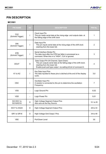
PIN DESCRIPTION<br />
<strong>MC3501</strong><br />
PIN NAME I/O DESCRIPTION PIN No.<br />
CLK<br />
(Schmitt Trigger)<br />
DIN<br />
(Schmitt Trigger)<br />
STB<br />
(Schmitt Trigger)<br />
DOUT O<br />
K1 to K2 I<br />
OSC I<br />
I<br />
I<br />
I<br />
Clock Input Pin<br />
This pin reads serial data at the rising edge and outputs data at<br />
the falling edge of the shift clock<br />
Data Input Pin<br />
This pin inputs serial data at the rising edge of the shift clock<br />
(starting from the lower bit)<br />
Serial Interface Strobe Pin<br />
The data input after the STB has fallen is processed as a<br />
command. When this in is “HIGH”, CLK is ignored.<br />
Data Output Pin (N-Channel, Open-Drain)<br />
This pin outputs serial data at the falling edge of the shift clock.<br />
(starting from the lower bit)<br />
Enable push-pull type output via setting b5,b4 of command 4.<br />
Key Data Input Pins<br />
The data inputted to these pins is latched at the end of the display<br />
cycle.<br />
Oscillator Input Pin<br />
A resistor is connected to this pin to determine the oscillation<br />
Frequency.<br />
VSS - Logic Ground Pin 8,52<br />
VDD - Logic Power Pin 9,51<br />
SG1/KS1 to<br />
SG16/KS16<br />
O<br />
High-Voltage Segment Output Pins<br />
Also acts as the Key Source.<br />
1<br />
2<br />
3<br />
4<br />
5,6<br />
7<br />
10 to 25<br />
SG17 to SG24 O High-Voltage Segment Output Pins 26 to 33<br />
GR1 to GR16 O High-Voltage Grid Output Pins 34 to 49<br />
VEE - Pull-Down Level 50<br />
December 17, 2010 Ver.2.3 5/24