50. J. M. Hvam, S. Stobbe, and P. Lodahl - Quantum Photonics
50. J. M. Hvam, S. Stobbe, and P. Lodahl - Quantum Photonics
50. J. M. Hvam, S. Stobbe, and P. Lodahl - Quantum Photonics

Create successful ePaper yourself
Turn your PDF publications into a flip-book with our unique Google optimized e-Paper software.
Phys. Status Solidi B 248, No. 2, 375–383 (2011) / DOI 10.1002/pssb.201000634<br />
<strong>Quantum</strong>-dot excitons in<br />
nanostructured environments<br />
Jørn M. <strong>Hvam</strong> * , Søren <strong>Stobbe</strong>, <strong>and</strong> Peter <strong>Lodahl</strong><br />
DTU Fotonik, Department of <strong>Photonics</strong> Engineering, Technical University of Denmark, 2800 Kgs. Lyngby, Denmark<br />
Received 7 July 2010, accepted 4 October 2010<br />
Published online 9 November 2010<br />
Keywords oscillator strength, photonic crystals, quantum-dot excitons, spin-flip<br />
* Corresponding author: e-mail jmhv@fotonik.dtu.dk, Phone: þ45 4525 5758, Fax: þ45 4593 6581<br />
The interaction between light <strong>and</strong> quantum-dot (QD) excitons is<br />
strongly influenced by the environment in which the QD is<br />
placed. We have investigated the interaction by measuring the<br />
time-resolved spontaneous-emission rate of QD excitons in<br />
different nanostructured environments. Thereby, we have<br />
determined the oscillator strength, quantum efficiency <strong>and</strong><br />
spin-flip rates of QD excitons as well as their dependencies on<br />
emission wavelength <strong>and</strong> QD size. Enhancement <strong>and</strong> inhibition<br />
of QD spontaneous emission in photonic crystal membranes<br />
(PCMs) is observed. Efficient coupling to PCM waveguides is<br />
demonstrated <strong>and</strong> the influence of disorder is discussed. The<br />
findings have a strong bearing on future nanophotonic devices.<br />
1 Introduction The interaction between excitons <strong>and</strong><br />
light, as e.g. manifested by the spontaneous emission rate, is<br />
essentially governed by two factors: The oscillator strength<br />
which describes the strength of the exciton–photon interaction,<br />
as can be calculated on a quantum-mechanical basis<br />
[1], <strong>and</strong> the density of optical states (DOS) to interact with<br />
[2]. The latter can be calculated classically from Maxwell’s<br />
equations once the material environment is specified.<br />
In the weak-coupling limit the light–matter interaction<br />
strength can be calculated perturbatively leading to Fermi’s<br />
golden rule. In the strong-coupling limit, the full exciton–<br />
photon Hamiltonian is diagonalised leading to a new quasi<br />
particle the (exciton-)polariton [3] with a mixed exciton/<br />
photon character depending on the detuning from the bare<br />
exciton resonance. Prominent examples of strong coupling<br />
are (Wannier) exciton-polaritons in bulk wide-gap II–VI<br />
semiconductors [4] <strong>and</strong> cavity-polaritons in III–V semiconductor<br />
microcavities [5]. Recently, strong coupling has also<br />
been observed between single quantum-dot (QD) excitons<br />
<strong>and</strong> various types of nanocavities [6, 7]. The latter two cases<br />
are examples showing that strong coupling can also be<br />
achieved by modifying the local density of optical states<br />
physica<br />
pss<br />
www.pss-b.com<br />
status<br />
solidi<br />
basic solid state physics<br />
Feature Article<br />
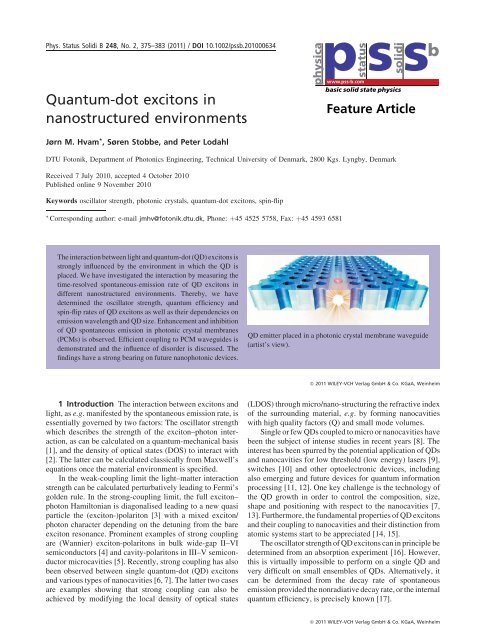
QD emitter placed in a photonic crystal membrane waveguide<br />
(artist’s view).<br />
b<br />
ß 2011 WILEY-VCH Verlag GmbH & Co. KGaA, Weinheim<br />
(LDOS) through micro/nano-structuring the refractive index<br />
of the surrounding material, e.g. by forming nanocavities<br />
with high quality factors (Q) <strong>and</strong> small mode volumes.<br />
Single or few QDs coupled to micro or nanocavities have<br />
been the subject of intense studies in recent years [8]. The<br />
interest has been spurred by the potential application of QDs<br />
<strong>and</strong> nanocavities for low threshold (low energy) lasers [9],<br />
switches [10] <strong>and</strong> other optoelectronic devices, including<br />
also emerging <strong>and</strong> future devices for quantum information<br />
processing [11, 12]. One key challenge is the technology of<br />
the QD growth in order to control the composition, size,<br />
shape <strong>and</strong> positioning with respect to the nanocavities [7,<br />
13]. Furthermore, the fundamental properties of QD excitons<br />
<strong>and</strong> their coupling to nanocavities <strong>and</strong> their distinction from<br />
atomic systems start to be appreciated [14, 15].<br />
The oscillator strength of QD excitons can in principle be<br />
determined from an absorption experiment [16]. However,<br />
this is virtually impossible to perform on a single QD <strong>and</strong><br />
very difficult on small ensembles of QDs. Alternatively, it<br />
can be determined from the decay rate of spontaneous<br />
emission provided the nonradiative decay rate, or the internal<br />
quantum efficiency, is precisely known [17].<br />
ß 2011 WILEY-VCH Verlag GmbH & Co. KGaA, Weinheim
physica<br />
p status<br />
s<br />
solidi<br />
s<br />
b<br />
376 J. M. <strong>Hvam</strong> et al.: <strong>Quantum</strong>-dot excitons in nanostructured environments<br />
In the present paper we will focus our attention on the<br />
study of spontaneous emission from QD excitons in various<br />
nanostructured environments. In the first part (Section 3), we<br />
will make use of a modified LDOS to determine fundamental<br />
QD exciton parameters like quantum efficiency, oscillator<br />
strength [17, 18] <strong>and</strong> spin-flip rates [19]. In the second part<br />
(Section 4), we will demonstrate how one can modify <strong>and</strong><br />
control the spontaneous emission rate [20, 21], by operating<br />
in the weak-coupling limit, into specific optical modes [22]<br />
by proper structuring of the immediate surroundings of the<br />
QD excitons. The investigations are of fundamental<br />
character <strong>and</strong> are considered as prerequisites to venture<br />
further into all-solid-state quantum optics/photonics with<br />
applications in future integrated optics <strong>and</strong> nanophotonics<br />
including single-photon devices for quantum communication<br />
<strong>and</strong> quantum computing [11, 12].<br />
2 Experimental<br />
2.1 Self-assembled quantum dots The QDs<br />
investigated here are self-assembled Stranskii–Krastanov<br />
InAs/GaAs or InxGa1 xAs/GaAs dots grown by molecular<br />
beam epitaxy on (001) oriented GaAs substrates as described<br />
in detail in Refs.[17, 18]. The InAs dots are typically<br />
relatively small, around 20 nm in diameter <strong>and</strong> with average<br />
height of about 7 nm, with a significant spread giving rise to<br />
an inhomogeneous broadening of 60–80 meV of the groundstate<br />
transition from an ensemble of these QDs. The areal<br />
density of the InAs QDs, as determined by atomic force<br />
microscopy (AFM), is typically 250 mm 2 , corresponding to<br />
an average distance of 60 nm between QDs. This excludes<br />
any significant interaction between QDs so that all<br />
measurements can be considered ensemble-averaged values<br />
of the properties of individual QDs. The In xGa 1 xAs<br />
(x ¼ 0.3) QDs are typically larger, 40–70 nm in diameter,<br />
with a correspondingly lower areal density of 100 mm 2 .<br />
2.2 Interface <strong>and</strong> photonic crystal structures<br />
The single layer of QDs described above are embedded in<br />
layers of GaAs <strong>and</strong> AlAs allowing for further processing of<br />
samples to be investigated. For interface studies, the QD<br />
layer is overgrown by 300 nm of GaAs. The wafer was then<br />
processed by st<strong>and</strong>ard UV lithography <strong>and</strong> wet chemical<br />
etching in five subsequent steps with nominal etch depths of<br />
160, 80, 40, 20, <strong>and</strong> 10 nm by which was obtained 32 fields<br />
with specific distances (spaced by 10 nm) from the QDs to<br />
the semiconductor surface (see Ref. [17] for further details).<br />
A schematic illustration of the resulting sample is shown<br />
in Fig. 1(a).<br />
For photonic crystal studies, a sacrificial layer of AlAs is<br />
first grown followed by a 150-nm layer of GaAs with a single<br />
layer of InAs self-assembled QDs in the centre. The photonic<br />
crystal structures are then formed by electron-beam<br />
lithography <strong>and</strong> dry etching followed by wet etching of the<br />
sacrificial AlAs layer to form the photonic crystal membrane<br />
(PCM). The PCM consists of holes arranged in a triangular<br />
lattice with hole radius r <strong>and</strong> lattice constant a <strong>and</strong> a fill factor<br />
around 66% (r/a 0.3), see details in Refs. [21, 22]. In the<br />
Figure 1 (a) Schematic drawing of the interface sample; (b) SEM<br />
picture of photonic crystal membrane with W1 waveguide.<br />
PCM a photonic crystal waveguide (PCW) can be formed by<br />
omitting one row of holes (W1 waveguide). In Fig. 1(b) is<br />
shown a SEM picture of a typical PCM with a W1<br />
waveguide.<br />
2.3 Optical characterisation The QD excitons have<br />
been studied by time-resolved micro-photoluminescence<br />
(m-PL). The samples were placed in a helium flow cryostat<br />
mounted on precision translational stages <strong>and</strong> excited by<br />
subpicosecond or picosecond pulses from a mode-locked<br />
Ti:sapphire laser with a repetition rate of 78 MHz <strong>and</strong><br />
emitting at around 800 nm. The excitation spot size could be<br />
varied from >100 mm down to 1.4 mm, which is also the<br />
ultimate spatial resolution of the emission which is sent<br />
through a spectrometer <strong>and</strong> detected by either a CCD camera<br />
for recording full spectra or an avalanche photodiode (APD)<br />
for time-resolved measurement, see Fig. 2. Thus, both<br />
ensemble measurements <strong>and</strong>, by combining spatial <strong>and</strong><br />
spectral resolution, single-dot PL measurements can be<br />
performed with a time resolution down to 40 ps. All<br />
experiments are performed at cryogenic temperatures,<br />
normally around 10 K. Further details on the experimental<br />
techniques can be found in Refs. [17, 22].<br />
3 <strong>Quantum</strong>-dot excitons For excitons in QDs there<br />
are three different regimes of quantisation depending on the<br />
relative importance of the electron–hole Coulomb interaction<br />
<strong>and</strong> the quantisation energies of electrons <strong>and</strong> holes in<br />
the confining QD potential [23].<br />
For small QDs with an average radius R a x, where a x is<br />
the (bulk) exciton Bohr radius, the electron <strong>and</strong> hole<br />
Figure 2 Schematics of the experimental setup. BS: beamsplitter;<br />
CCD: charge-coupled device/camera; APD: avalanche photo diode.<br />
ß 2011 WILEY-VCH Verlag GmbH & Co. KGaA, Weinheim www.pss-b.com
Phys. Status Solidi B 248, No. 2 (2011) 377<br />
quantisation energies dominate over the Coulomb energy. In<br />
this so-called strong confinement (SC) limit, exciton effects<br />
are negligible <strong>and</strong> the oscillator strength can be expressed as<br />
[17, 18]<br />
fSCðvÞ ¼ Ep<br />
hv FeðvÞ jh jFhðvÞij<br />
2 Ep<br />
; (1)<br />
hv<br />
where Ep is the Kane energy for the semiconductor<br />
constituting the QD, hv is the transition energy, <strong>and</strong><br />
FeðhÞðvÞ is the envelope of the electron (hole) wavefunction.<br />
For intermediate-sized QDs (R ax) where the Coulomb<br />
<strong>and</strong> quantisation energies have to be treated on an equal<br />
footing, there is no simple solution for the oscillator strength,<br />
whereas for large QDs, with R ax, the quantisation<br />
energies are small compared to the Coulomb energy. In this<br />
weak confinement (WC) limit, the exciton wavefunction is<br />
essentially unaltered by the confinement <strong>and</strong> only the<br />
translational energy of the exciton is quantised in the QD<br />
potential. Correspondingly, the oscillator strength is essentially<br />
the bulk exciton oscillator strength [24]<br />
fWCðvÞ ¼fxðvÞ ¼ Ep Vcoh<br />
hv pa3 x<br />
Ep<br />
hv<br />
VQD<br />
pa3 x<br />
; (2)<br />
where Vcoh is the coherence volume of the exciton <strong>and</strong> VQD<br />
is the volume of the QD.<br />
Specifically, for InxGa1 xAs self-assembled QDs with<br />
E p ¼ E p(x) ¼ (28.8 7.3x) eV, <strong>and</strong> assuming infinite barriers<br />
in the growth direction <strong>and</strong> a parabolic confinement potential<br />
in the plane perpendicular to it, one can obtain [25, 26]<br />
fWCðv; xÞ<br />
2EpðxÞ<br />
hv<br />
L<br />
ax<br />
2<br />
; (3)<br />
where L is the diameter of the QD, defined as four st<strong>and</strong>ard<br />
deviations of the Gaussian centre-of-mass wavefunction.<br />
Thus, for large QDs there is the potential for ‘‘giant’’<br />
oscillator strength [27] provided the exciton is coherent over<br />
the whole QD volume. It should also be mentioned that the<br />
above analysis assumes the dipole approximation to be valid<br />
for all QDs, which may not hold for large QDs.<br />
Figure 3 Calculated oscillator strength for InxGa1 xAs QDs with<br />
x ¼ 0, x ¼ 0.3 <strong>and</strong> x ¼ 1.0. In the weak confinement limit (dashed<br />
lines) fWC increases quadratically with the exciton (QD) size,<br />
whereas in the strong confinement limit f SC 23.2 (17.1) for GaAs<br />
(InAs).<br />
Feature<br />
Article<br />
Applying Eqs. (1) <strong>and</strong> (3), the upper bounds for the<br />
oscillator strength are plotted in Fig. 3 in the SC (solid lines)<br />
<strong>and</strong> WC (dashed lines) limits, respectively for InxGa1 xAs<br />
QDs with x ¼ 0, x ¼ 0.3 <strong>and</strong> x ¼ 1.0. Thus, oscillator<br />
strengths beyond 100 should be achievable in large<br />
In0.3Ga0.7As QDs facilitating strong coupling between single<br />
large QDs <strong>and</strong> nanocavities.<br />
Indeed strong coupling has been observed in such<br />
systems [6]. We have pursued a different route to directly<br />
determine the oscillator strength from the radiative decay<br />
rate of QD excitons in a nanostructured environment<br />
[17, 18].<br />
3.1 Determination of oscillator strength The<br />
radiative recombination rate Grad(v) of QD excitons in a<br />
homogeneous medium with refractive index n can be<br />
calculated from Fermi’s golden rule <strong>and</strong> expressed by the<br />
oscillator strength fx(v) <strong>and</strong> the DOS rhom(v) ¼ n 3 v 2 /p 2 c 3<br />
[18]<br />
G radðvÞ ¼ pe2 fxðvÞr homðvÞ<br />
6e0m0n 2 ¼ ne2 v 2<br />
6pe0m0c 3 fxðvÞ; (4)<br />
where e0, m0 <strong>and</strong> c are the vacuum dielectric constant, the<br />
free electron mass, <strong>and</strong> the velocity of light in vacuum,<br />
respectively. However, in order to determine Grad(v) from<br />
the PL decay of QD excitons after a short-pulse excitation<br />
one needs to know also the nonradiative decay rate G nrad(v),<br />
i.e. the internal quantum efficiency<br />
G radðvÞ<br />
hintðvÞ ¼<br />
G radðvÞþG nradðvÞ ¼ G radðvÞ<br />
: (5)<br />
G ðvÞ<br />
The radiative <strong>and</strong> non-radiative recombination rates can<br />
be separated by measuring the decay rates of QD excitons<br />
placed at different positions r in an environment with a<br />
known LDOS r l(v,r) [28]. We have done this for the sample<br />
shown in Fig. 1(a), i.e. measured [17, 18]<br />
G ðv; zÞ ¼G radðvÞ r lðv; zÞ<br />
r homðvÞ þ G nradðvÞ; (6)<br />
Figure 4 The LDOS as a function of distance z to a GaAs–air<br />
interface for a dipole oriented parallel (black curve) or perpendicular<br />
(grey curve) to the interface.<br />
www.pss-b.com ß 2011 WILEY-VCH Verlag GmbH & Co. KGaA, Weinheim
physica<br />
p status<br />
s<br />
solidi<br />
s<br />
b<br />
378 J. M. <strong>Hvam</strong> et al.: <strong>Quantum</strong>-dot excitons in nanostructured environments<br />
where rl(v,z) is the projection of the LDOS along the<br />
direction of the transition dipole moment of the QD exciton<br />
<strong>and</strong> shown in Fig. 4 as a function of the distance z to a GaAs–<br />
air interface for two dipole orientations parallel <strong>and</strong><br />
perpendicular to the interface. For Stranskii–Krastanov<br />
grown InAs/GaAs QDs the transition dipole moment is<br />
oriented perpendicular to the growth direction, i.e. parallel<br />
to the GaAs–air interfaces of the sample sketched in<br />
Fig. 1(a).<br />
Examples of measured PL decay curves are shown in the<br />
inset of Fig. 5(a) for two different distances from the<br />
interface. The decays are bi-exponential with a slow decay<br />
rate Gs 0.1 ns 1 <strong>and</strong> a fast decay rate Gf which is about one<br />
order of magnitude larger. The slow decay rate is largely<br />
independent of the distance to the surface as seen in the lower<br />
curve of Fig. 5(a). It is ascribed to the influence of the dark<br />
exciton states, as we will discuss in the next section.<br />
The variation of the fast decay rate with the distance to<br />
the interface is shown as the upper curve in Fig. 5(a). The<br />
points are the measured decay rates <strong>and</strong> the solid curve is a fit<br />
by Eq. (6) with the known values of rl(v,z) <strong>and</strong> rhom(v). The<br />
fit is excellent for distances z > 100 nm, <strong>and</strong> from this fit<br />
the radiative recombination rate Grad(v) as well as the<br />
nonradiative recombination rate Gnrad(v) are uniquely<br />
determined without any further assumptions about the<br />
sample. The deviations for z < 100 nm could be related to<br />
dissipation at the sample surface [17], but do not influence<br />
the determination of the QD parameters.<br />
The oscillator strength f x(v) <strong>and</strong> the internal quantum<br />
efficiency h int(v) are determined by Eqs. (4) <strong>and</strong> (5),<br />
respectively. The results are shown in Fig. 6(a) as a function<br />
of transition energy across the inhomogeneously broadened<br />
Figure 5 (online colour at: www.pss-b.com) (a) Measured<br />
decay rates as a function of distance z to the GaAs–air interface<br />
(solid squares). Calculated decay rates (solid curve) applying the<br />
LDOS projected onto a dipole oriented parallel to the interface. The<br />
inset shows PL decays for two different distances to the interface<br />
perfectly fitted by bi-exponential decays with G f¼ 0:91 ns 1 <strong>and</strong><br />
G s¼ 0:09 ns 1<br />
for z ¼ 109 nm <strong>and</strong> G f¼ 1:15 ns 1<br />
<strong>and</strong><br />
G s¼ 0:10 ns 1 for z ¼ 170 nm. (b) Goodness-of-fit x2 R for all distances<br />
to the interface.<br />
Figure 6 (a) Oscillator strength (solid squares, left scale) <strong>and</strong><br />
quantum efficiency (open squares, right scale) versus emission<br />
photon energy. (b) Measured (squares) <strong>and</strong> calculated (solid curve)<br />
overlap of the envelope wavefunctions of electrons <strong>and</strong> holes.<br />
PL spectrum from an ensemble of InAs/GaAs QD excitons<br />
[17]. The QDs examined in Fig. 6 are relatively small<br />
(diameter 20 nm, height 6 nm) whereby the excitons can<br />
be considered to be in the SC limit. Applying Eq. (1), we can<br />
then estimate the overlap integral of the electron <strong>and</strong> hole<br />
wavefunctions. The result is shown as experimental points in<br />
Fig. 6(b) <strong>and</strong> compared with a model calculation based on<br />
lens-shaped QDs with a size distribution giving rise to<br />
ground state transitions matching the inhomogeneously<br />
broadened PL spectrum [17]. More details of these<br />
experiments can be found in Refs. [17, 18].<br />
It has been argued that oscillator strengths well beyond<br />
what is determined above are necessary to obtain strong<br />
coupling between a single QD <strong>and</strong> a high-Q nanocavity [29].<br />
We have performed the above measurements also on<br />
In 0.3Ga 0.7As/GaAs QDs with a diameter of 40 nm which,<br />
according to Eq. (3), should give rise to an oscillator strength<br />
fWC > 100 (Fig. 3). However, oscillator strengths in the same<br />
range as for the smaller QDs were found, but with a<br />
significantly lower quantum efficiency [26]. We may<br />
therefore conclude that the coherence volume (area) of the<br />
excitons in these QDs is smaller than the actual volume (area)<br />
of the QDs, e.g. by excitons being further localised by a<br />
fluctuating potential from strain <strong>and</strong>/or alloy disorder.<br />
3.2 Dark excitons <strong>and</strong> spin-flip rates In the above<br />
analysis we neglected the slow part of the decay. However,<br />
the decay curves in Fig. 5(a) are fitted excellently with the biexponential<br />
function<br />
IðtÞ ¼Afe G ft þ Ase G st ; (7)<br />
where the fast <strong>and</strong> slow amplitudes, A f <strong>and</strong> A s, are included<br />
as parameters. With this additional information it is possible<br />
to gain further insight in the QD exciton dynamics,<br />
including the spin flips connecting the bright <strong>and</strong> dark<br />
ß 2011 WILEY-VCH Verlag GmbH & Co. KGaA, Weinheim www.pss-b.com
Phys. Status Solidi B 248, No. 2 (2011) 379<br />
Figure 7 Exciton level scheme with bright, dark <strong>and</strong> ground states.<br />
The transition rates are indicated <strong>and</strong> explained in the text.<br />
exciton states that are initially both populated after a shortpulse<br />
excitation into the continuum states.<br />
Figure 7 shows the fine structure of the lowest exciton<br />
state for InAs/GaAs QDs. The exciton is formed by the<br />
conduction-b<strong>and</strong> electron state (spin 1/2) <strong>and</strong> the heavy-hole<br />
valence-b<strong>and</strong> state (total angular momentum 3/2). Thus, four<br />
exciton states can be formed characterised by the projections<br />
of the total angular momentum onto the growth axis with the<br />
values 1or 2for bright <strong>and</strong> dark excitons, respectively.<br />
The bright-exciton level jbiis typically a few hundred meV<br />
above the dark-exciton level jdi. The splitting is determined<br />
by the exchange coupling between electron <strong>and</strong> hole spins.<br />
The bright excitons can decay into the ground state jieither g<br />
Þ. The dark excitons<br />
radiatively ðgradÞ or nonradiativelyðgb nrad<br />
can only recombine nonradiatively ðgd nrad<br />
Þ. Alternatively,<br />
they can be transformed into bright excitons via a phononmediated<br />
spin-flip process with a rate g db [30, 31]. The<br />
reverse process may also occur with a rate g bd.<br />
Assuming that the spin-flip rates are much slower than<br />
both radiative <strong>and</strong> nonradiative recombination rates, we can<br />
identify the decay rates G f ffi g rad þ g b nrad <strong>and</strong> G s ffi g d nrad .<br />
Thus, the spin-flip rates cannot be determined directly from<br />
these decay rates. However, the amplitudes of the fast <strong>and</strong><br />
slow components carry additional information including the<br />
spin-flip rates [19]:<br />
AfðzÞ<br />
AsðzÞ ¼ G fðzÞ G sðzÞ nbðt ¼ 0Þ<br />
; (8)<br />
gdbðzÞ ndðt ¼ 0Þ<br />
where nb/d(t ¼ 0) are the initial populations of bright/dark<br />
excitons, which can be considered equal for very low<br />
density of non-resonant excitation. In our experiments, the<br />
excitation density was typically such that the initial average<br />
population was 0.1 exciton per QD. Thus, there is a finite<br />
probability to form biexcitons that will recombine<br />
radiatively <strong>and</strong> always leave bright excitons behind. This<br />
results in a slight overweight of bright excitons over dark<br />
excitons: nbðt¼ 0Þ=ndðt¼ 0Þ 1:25 [19].<br />
The spin-flip rate can then be determined from Eq. (8)<br />
<strong>and</strong> the result is shown in Fig. 8 as a function of distance to<br />
the interface <strong>and</strong> for different transition energies across the<br />
inhomogeneously broadened PL line [19]. As it turns out, the<br />
spin-flip rate increases in an exponential fashion when<br />
approaching the interface with a characteristic length of 25–<br />
110 nm. This length is comparable to the wavelength of<br />
Feature<br />
Article<br />
Figure 8 (onlinecolourat:www.pss-b.com)Thespin-flipratesasa<br />
function of distance z to the interface for different emission energies<br />
1.170, 1.187, 1.204, 1.216, 1.252 <strong>and</strong> 1.272 eV counted from below<br />
at z ¼ 300 nm. The solid curves are fits to the experimental points<br />
assuming an exponential decay of the rates away from the interface<br />
with characteristics lengths of 25–110 nm.<br />
acoustic phonons with energies matching the exchange<br />
splitting between bright <strong>and</strong> dark excitons. Thus, the increase<br />
could be caused by an enhancement of the acoustic phonons<br />
at the interface [19].<br />
The spin-flip rate also depends strongly on the emission<br />
energy <strong>and</strong> thereby the QD size. The values furthest away<br />
from the interface are plotted in Fig. 9 as a function of<br />
emission energy <strong>and</strong> are seen to vary from 6 ns 1 at 1.170 eV<br />
to 13 ns 1 at 1.272 eV. A calculation of the spin-flip rate<br />
based on short-range exchange interaction <strong>and</strong> acoustic<br />
phonons [31] produce the same trend in energy dependence,<br />
but at rates that are two orders of magnitude lower (dashed<br />
curve in Fig. 9). This discrepancy can be reduced somewhat<br />
by varying the composition, size <strong>and</strong> shape of the QDs (solid<br />
curve in Fig. 9), but still without a perfect fit to the<br />
experimental results [19]. Thus additional processes are<br />
likely to contribute to the exciton spin flips in QDs.<br />
4 <strong>Quantum</strong>-dots in photonic crystals In the<br />
above, we have studied the influence of very simple<br />
modifications of the QD environment. More dramatic<br />
changes of the light–matter interaction can be achieved in<br />
Figure 9 Measured spin-flip rates (solid squares) at different emission<br />
energies <strong>and</strong> far from the interface (z ¼ 302 nm). The dashed<br />
curve is a model calculation reproducing the energy dependence of<br />
the radiative decay rate (Fig. 6) <strong>and</strong> the solid curve is calculated with<br />
parameters optimised to fit the measured spin-flip rates.<br />
www.pss-b.com ß 2011 WILEY-VCH Verlag GmbH & Co. KGaA, Weinheim
physica<br />
p status<br />
a photonic crystal environment where spontaneous emission<br />
from QD excitons can be strongly enhanced or inhibited<br />
depending on the emission energy in relation to the photonic<br />
b<strong>and</strong> structure of the photonic crystal [20]. Here we will<br />
study the spontaneous emission rate of InAs/GaAs QD<br />
excitons embedded in a two-dimensional PCM as described<br />
in Section 2.2 [Fig. 1(b)]. It is of particular interest to study<br />
the emission rate in the spectral region in <strong>and</strong> around the b<strong>and</strong><br />
gap of the PCM [21].<br />
Since the ground-state transition energy of QD excitons<br />
embedded in the membrane is relatively fixed, we prepared a<br />
series of PCMs with lattice constant a (pitch) ranging from<br />
180 to 470 nm in steps of 10 nm <strong>and</strong> with constant fill factor<br />
ðr=a ¼ 0:313 0:006Þ. For the whole series, we then<br />
measured time resolved PL decay at a fixed wavelength<br />
(l ¼ 980 nm) after a short-pulse excitation at a fixed intensity<br />
into the GaAs barrier material [21].<br />
The result is shown in Fig. 10, where we observe a<br />
pronounced slow down of the decay, indicating a strong<br />
inhibition of the spontaneous emission, in the region<br />
0:26 a=l 0:35 for which the emission wavelength is<br />
within the b<strong>and</strong> gap of the corresponding PCM. The PL<br />
decays in Fig. 10(a) are strongly non-exponential (multiexponential)<br />
which is to be expected since the observed PL<br />
decay is an average over an ensemble of QDs with different<br />
positions <strong>and</strong> orientations within the PCM <strong>and</strong> thereby<br />
different LDOS. Still, we can define a mean decay time<br />
tm ¼ R 1<br />
s<br />
solidi<br />
s<br />
b<br />
380 J. M. <strong>Hvam</strong> et al.: <strong>Quantum</strong>-dot excitons in nanostructured environments<br />
0 tIðtÞdt= R 1<br />
0 IðtÞdt to characterise the decay rates<br />
in Fig. 10(a). The corresponding mean decay rates t 1<br />
m are<br />
plotted in Fig. 10(b) as solid squares <strong>and</strong> compared with a<br />
model calculation [32] shown as open squares. The measured<br />
reference decay rate is t 1<br />
m ¼ 0:75 ns 1 in the absence of the<br />
PCM. Thus, within the b<strong>and</strong> gap we observe a sixfold<br />
reduction/inhibition of the decay rate, whereas an increase<br />
(up to 30%) of the decay rate is observed just outside the b<strong>and</strong><br />
Figure 10 (online colour at: www.pss-b.com) (a) Colour-coded<br />
contour plots of normalised time-resolved decay curves <strong>and</strong><br />
(b) extracted mean decay rates (solid squares) <strong>and</strong> simulated values<br />
(open squares) for different lattice constants normalised to the<br />
emission wavelength. The b<strong>and</strong>-gap effect is clearly seen in the<br />
region 0.26 < a/l < 0.35.<br />
gap. It should be noted that the measured decay rates include<br />
nonradiative decays that are unaffected by the variations in<br />
the LDOS.<br />
These investigations serve as a background for further<br />
studies of the strong enhancement (Purcell effect) of QD<br />
exciton emission in particular nanocavity modes within the<br />
b<strong>and</strong> gap of PCMs. In the weak-coupling limit for QDs in a<br />
micro/nanocavity two parameters are essential to describe<br />
the coupling efficiency. The Purcell factor Fp is the factor<br />
with which the spontaneous emission rate is enhanced in the<br />
cavity over the emission rate in a homogeneous medium. The<br />
b-factor is the fraction of all the emitted photons that are<br />
emitted into the specific cavity mode. The latter is important<br />
for an efficient harvesting of light emission for a given<br />
purpose. It is of particular interest to couple the emitted<br />
photons into a guided mode [33, 34] that can lead the photons<br />
efficiently to the point of use.<br />
4.1 Coupling to photonic crystal waveguides<br />
We have experimentally investigated the coupling of single<br />
QDs to a PCM waveguide of the type W1 shown in Fig. 1(b)<br />
[22, 35]. In the membrane (150-nm thick) a single layer of<br />
InAs QDs is embedded with a density of 250 mm 1 <strong>and</strong> a<br />
ground-state emission wavelength around 960 nm. The QDs<br />
are excited from the surface in the m-PL setup sketched in<br />
Fig. 2 by 2-ps pulses from a Ti:sapphire laser emitting at<br />
800 nm <strong>and</strong> strongly focused through a microscope objective<br />
with high numerical aperture (NA ¼ 0.8). The QD exciton<br />
emission is detected through the same microscope lens with a<br />
resulting spatial resolution of 1.4 mm. The combination of<br />
the spatial resolution <strong>and</strong> the spectral resolution (0.15 nm)<br />
allows for the detection of single-QD emission lines from an<br />
ensemble of excited QDs with different positions <strong>and</strong><br />
orientations with respect to the waveguide, <strong>and</strong> thereby<br />
possibly different couplings to it. This is reflected in the<br />
different intensities of the emission lines, but more distinctly<br />
in the measured radiative decay rate of the different lines. A<br />
large group of QDs show a slow decay that is well fitted with<br />
a single-exponential (decay rate 0.05 ns 1 ) representing a<br />
QD that is uncoupled to the waveguide <strong>and</strong> with a radiative<br />
decay strongly inhibited by the surrounding photonic crystal.<br />
Other QDs showed a faster decay well fitted by a biexponential<br />
decay. The fast component is representing the<br />
radiative decay coupled to the waveguide <strong>and</strong> the slow<br />
component is due to dark excitons as discussed in Section<br />
3.2. The fast rate is up to 27 times faster than the uncoupled<br />
QD demonstrating that the QD emission can be coupled very<br />
efficiently to a PCM waveguide in agreement with recent<br />
theoretical proposals [33, 34].<br />
A large number of measured decay rates on a sample<br />
with lattice constant a ¼ 256 nm was analysed in Ref. [22]<br />
showing that the decay rate, <strong>and</strong> thereby the coupling to the<br />
waveguide, is increasing strongly as the frequency<br />
approaches the cut-off frequency of the PCM waveguide,<br />
i.e. as the group index increases in the slow-light region.<br />
The coupling efficiency of the QDs to the PCM<br />
waveguide is quantified by the b-factor, which we can<br />
ß 2011 WILEY-VCH Verlag GmbH & Co. KGaA, Weinheim www.pss-b.com
Phys. Status Solidi B 248, No. 2 (2011) 381<br />
Figure 11 MeasuredQD decayrates(opensquares) onaPCMW1waveguide<br />
(inset) as a function of detuning from the waveguide cutoff<br />
wavelength at 969 nm. The solid curve is calculated from the<br />
simulated group velocity in a lossless waveguide.<br />
calculate from<br />
G wg<br />
b ¼<br />
G wg þ G rad þ G nrad<br />
¼ G res G non-res<br />
; (9)<br />
G res<br />
where G wg is the decay rate into the waveguide mode, G rad<br />
is the decay rate to non-guided modes, <strong>and</strong> G nrad is the<br />
intrinsic nonradiative decay rate. G res (G non-res) is the<br />
observed decay rate of a coupled (uncoupled) QD. In<br />
Ref. [22] it was found that the b-factor approaches 0.9 near<br />
the cut-off frequency of the waveguide. We have also varied<br />
the coupling of an individual QD to the W1 waveguide by<br />
temperature tuning the emission of the QD through the<br />
wavelength region around the cut-off wavelength of the<br />
waveguide [35]. The result is shown in Fig. 11 (open<br />
squares), from which again a high b-factor (0.85) can be<br />
deduced when the QD is resonant with the slow-light region<br />
of the waveguide. The decay rate of QDs coupled to a<br />
lossless PCM waveguide is calculated from the simulated<br />
group velocity [33] <strong>and</strong> is shown as the solid curve in<br />
Fig. 11. At resonance the enhanced decay rate corresponds<br />
to a Purcell factor Fp ¼ G res=G 0¼ 5:2 where G 0 ¼ 1:1ns 1<br />
is the decay rate of the QD in a homogeneous medium. We<br />
have studied also a QD detuned by approximately 2nm<br />
<strong>and</strong> found an almost constant decay rate of 2ns 1 . Thus,<br />
an efficient coupling to the PCM waveguide has been<br />
demonstrated over a b<strong>and</strong>width larger than 5 nm [35]. This<br />
is in contrast to the narrow b<strong>and</strong>width of efficient coupling<br />
to high-Q nanocavities [36, 37].<br />
4.2 Influence of disorder It is obvious from the<br />
above that the radiative coupling of QDs to a PCM<br />
waveguide is strongly enhanced when the emission frequency<br />
approaches the waveguide cut-off frequency, i.e. in<br />
the slow-light region where not only the propagation of light<br />
is affected (velocity, dispersion), but where also losses, <strong>and</strong><br />
in particular scattering (in the waveguide plane <strong>and</strong> out-ofplane)<br />
due to disorder, are increased. This poses a serious<br />
problem for an efficient coupling of the QD (single-photon)<br />
emission to an external user. However, it can also be<br />
considered as resource for an alternative way of localising<br />
light in very small-volume cavities. We have shown that<br />
Feature<br />
Article<br />
Figure 12 (online colour at: www.pss-b.com) (a) Spectra of<br />
Anderson-localised modes for different degrees of engineered disorder.<br />
The waveguide cut-off is at 978 nm. Each spectrum is collected<br />
with the excitation <strong>and</strong> collection microscope objective at a<br />
fixedpositiononthewaveguide.Thespectra areshiftedverticallyfor<br />
visual clarity. (b)Scan along the waveguide for3% disorder showing<br />
that the modes are indeed localised.<br />
indeed Anderson localisation [38] of waveguide modes in<br />
such a PCM waveguide with controlled additional disorder<br />
can be obtained [39]. Figure 12(a) shows the spectral<br />
signature of such Anderson-localised modes. The localised<br />
modes are predominant near the cut-off wavelength of the<br />
waveguide. That they are indeed localised is shown in<br />
Fig. 12(b), where the microscope objective is scanned along<br />
the waveguide in a sample with 3% engineered disorder. It is<br />
interesting to speculate to what extent these disorderlocalised<br />
modes can serve as an alternative to conventional<br />
nanocavities <strong>and</strong> open a new avenue towards all-solid-state<br />
cavity QED.<br />
5 Applications Due to the discrete nature of the<br />
electronic states in QDs they are often called artificial atoms<br />
<strong>and</strong> it is the combination of the atomistic character <strong>and</strong> the<br />
fact that they appear in a solid-state environment that make<br />
them attractive for many applications. Devices based on<br />
semiconductor QDs can easily be incorporated in integrated<br />
<strong>and</strong> scalable photonic <strong>and</strong> electronic circuits, <strong>and</strong> devices<br />
containing single, or a few, QDs coupled to a nanocavity can<br />
be miniaturised to the smallest scale allowed by the wave<br />
nature of light [40]. This limit can be pushed further down if<br />
metallic (plasmonic) structures are incorporated [41].<br />
www.pss-b.com ß 2011 WILEY-VCH Verlag GmbH & Co. KGaA, Weinheim
physica<br />
p status<br />
s<br />
solidi<br />
382 J. M. <strong>Hvam</strong> et al.: <strong>Quantum</strong>-dot excitons in nanostructured environments<br />
The two-level nature of the ground-state transition of QD<br />
excitons ensures that transparency <strong>and</strong> gain (inversion) can<br />
be attained with very modest pumping, <strong>and</strong> the efficient<br />
coupling to nanocavities with high Q <strong>and</strong> small mode volume<br />
paves the way to very compact, low-threshold lasers [40] <strong>and</strong><br />
switches. However, an efficient coupling off-chip remains a<br />
serious challenge.<br />
Single QDs are ideal single-photon emitters from the<br />
ground-state transition [12, 42]. If the QD is excited further<br />
to obtain a significant biexciton population, it can even serve<br />
as an efficient source of entangled photon pairs [43]. The<br />
challenges are to obtain a high rate of photons, or photon<br />
pairs, on dem<strong>and</strong> <strong>and</strong> also an efficient coupling to preferably<br />
an external optical fibre [44].<br />
6 Conclusions We have performed extensive studies<br />
of self-assembled InAs/GaAs QD excitons placed in<br />
different nanostructured environments, i.e. with the refractive<br />
index varying on the wavelength scale. We have<br />
exploited the resulting variation in the LDOS to obtain direct<br />
experimental measurements of the quantum efficiency,<br />
oscillator strength <strong>and</strong> spin-flip rates of the QD excitons.<br />
We have further demonstrated that the spontaneous emission<br />
rate of QD excitons can be manipulated very effectively by<br />
placing the QDs in different environments. In PCMs the<br />
spontaneous emission rate is significantly inhibited for<br />
wavelength within the photonic crystal b<strong>and</strong> gap. On the<br />
other h<strong>and</strong>, strong enhancement via the Purcell effect <strong>and</strong> an<br />
efficient coupling to localised modes in PCWs <strong>and</strong><br />
nanocavities can be obtained. The influence of disorder in<br />
the PCW has been studied <strong>and</strong> Anderson localisation of<br />
waveguide modes has been observed. These investigations<br />
are essential for the further underst<strong>and</strong>ing <strong>and</strong> exploitation of<br />
QD excitons in nanophotonics devices.<br />
Acknowledgements The authors gratefully acknowledge<br />
J. Johansen, T. Lund-Hansen, B. Julsgaard, H. Thyrrestrup,<br />
L. Sapienza, S. Smolka <strong>and</strong> P. D. Garcia for making their data<br />
available <strong>and</strong> T. Sünner, M. Kamp, T. Schlereth, S. Höfling <strong>and</strong><br />
A. Forchel for growth <strong>and</strong> processing of samples. Thanks are due<br />
to the Danish Research Agency <strong>and</strong> the Villum Kann Rasmussen<br />
Foundation for financial support.<br />
References<br />
s<br />
b<br />
[1] H. Haug <strong>and</strong> S. W. Koch, <strong>Quantum</strong> Theory of the Optical <strong>and</strong><br />
Electronic Properties of Semiconductors, second ed. (World<br />
Scientific, Singapore, 1993), p. 21.<br />
[2] R. Loudon, The <strong>Quantum</strong> Theory of Light (Oxford University<br />
Press, Oxford, 2000).<br />
[3] J. J. Hopfield, Phys. Rev. 112, 1555 (1958).<br />
[4] E. Gross, S. Permogorov, V. Travnikov, <strong>and</strong> A. Selkin, Solid<br />
State Commun. 16, 1971 (1972).<br />
[5] C. Weisbuch, M. Nishioka, A. Ishikawa, <strong>and</strong> Y. Arakawa,<br />
Phys. Rev. Lett. 69, 3314 (1992).<br />
[6] J. P. Reithmaier, G. Sek, A. Löffler, C. Hofmann, S. Kuhn,<br />
S. Reitzenstein, L. V. Keldysh, V. D. Kulakovskii, T. L.<br />
Reinecke, <strong>and</strong> A. Forchel, Nature 432, 197 (2004).<br />
[7] T. Yoshie, A. Scherer, J. Hendrickson, G. Khitrova, H. M.<br />
Gibbs, G. Rupper, C. Ell, O. B. Shchekin, <strong>and</strong> D. G. Deppe,<br />
Nature 432, 200 (2004).<br />
[8] A. Laucht, F. Hofbauer, N. Hauke, J. Angele, S. <strong>Stobbe</strong>,<br />
M. Kaniber, G. Böhm, P. <strong>Lodahl</strong>, M.-C. Amann, <strong>and</strong> J. J.<br />
Finley, New J. Phys. 11, 023034 (2009).<br />
[9] S. Reitzenstein, T. Heindel, C. Kistner, A. Rahimi-Iman,<br />
C. Schneider, S. Höfling, <strong>and</strong> A. Forchel, Appl. Phys. Lett.<br />
93, 061104 (2008).<br />
[10] X. Ma <strong>and</strong> S. John, Phys. Rev. Lett. 103, 233601 (2009).<br />
[11] A. Imamoglu, D. D. Awschalom, G. Burkard, D. P. DiVincenzo,<br />
D. Loss, M. Scherwin, <strong>and</strong> A. Small, Phys. Rev. Lett.<br />
83, 4204 (1999).<br />
[12] P. Michler, A. Kiraz, C. Becher, W. V. Schoenfeld, P. M.<br />
Petroff, L. Zhang, E. Hu, <strong>and</strong> A. Imamoglu, Science 290,<br />
2282 (2000).<br />
[13] C. Schneider, A. Huggenberger, T. Sünner, T. Heindel,<br />
M. Strauss, S. Göpfer, P. Weinmann, S. Reitzenstein,<br />
L. Worschech, M. Kamp, S. Höfling, <strong>and</strong> A. Forchel, Nanotechnology<br />
20, 434012 (2009).<br />
[14] K. Hennessy, A. Badolato, M. Wigner, D. Gerace, M. Atatüre,<br />
S. Gulde, S. Fält, E. L. Hu, <strong>and</strong> A. Imamoglu, Nature<br />
445, 896 (2007).<br />
[15] A. Naesby, T. Suhr, P. T. Kristensen, <strong>and</strong> J. Mørk, Phys. Rev.<br />
A 78, 045802 (2008).<br />
[16] D. Birkedal, J. Bloch, J. Shah, L. N. Pfeiffer, <strong>and</strong> K. West,<br />
Appl. Phys. Lett. 77, 2201 (2000).<br />
[17] J. Johansen, S. <strong>Stobbe</strong>, I. S. Nikolaev, T. Lund-Hansen, P. T.<br />
Kristensen, J. M. <strong>Hvam</strong>, W. L. Vos, <strong>and</strong> P. <strong>Lodahl</strong>, Phys. Rev.<br />
B 77, 073303 (2008).<br />
[18] S. <strong>Stobbe</strong>, J. Johansen, P. T. Kristensen, J. M. <strong>Hvam</strong>, <strong>and</strong><br />
P. <strong>Lodahl</strong>, Phys. Rev. B 80, 155307 (2009).<br />
[19] J. Johansen, B. Julsgaard, S. <strong>Stobbe</strong>, J. M. <strong>Hvam</strong>, <strong>and</strong><br />
P. <strong>Lodahl</strong>, Phys. Rev. B 81, 081304(R) (2010).<br />
[20] P. <strong>Lodahl</strong>, A. F. van Driel, I. S. Nikolaev, A. Irman,<br />
K. Overgaag, D. Vanmaekelbergh, <strong>and</strong> W. L. Vos, Nature<br />
430, 654 (2004).<br />
[21] B. Julsgaard, J. Johansen, S. <strong>Stobbe</strong>, T. Stolberg-Rohr,<br />
T. Sünner, M. Kamp, A. Forchel, <strong>and</strong> P. <strong>Lodahl</strong>, Appl. Phys.<br />
Lett. 93, 094102 (2008).<br />
[22] T. Lund-Hansen, S. <strong>Stobbe</strong>, B. Julsgaard, H. Thyrrestrup,<br />
T. Sünner, M. Kamp, A. Forchel, <strong>and</strong> P. <strong>Lodahl</strong>, Phys. Rev.<br />
Lett. 101, 113903 (2008).<br />
[23] C. Klingshirn, Semiconductor Optics, third ed. (Springer,<br />
Heidelberg, 2007), p. 392.<br />
[24] J. Bellessa, V. Voliotis, R. Grousson, X. L. Wang, M. Ogura,<br />
<strong>and</strong> H. Matsuhata, Phys. Rev. B 58, 9933 (1998).<br />
[25] M. Sugawara, Phys. Rev. B 51, 10743 (1995).<br />
[26] S. <strong>Stobbe</strong>, T. W. Schlereth, S. Höfling, A. Forchel, J. M.<br />
<strong>Hvam</strong>, P. <strong>Lodahl</strong>, arXiv:1006.5796, resubmitted to Phys.<br />
Rev. B.<br />
[27] E. Hanamura, Phys. Rev. B 37, 1273 (1988).<br />
[28] K. L. Drexhage, J. Lumin. 1-2, 693 (1970).<br />
[29] L. C. Andreani, G. Panzarini, <strong>and</strong> J.-M. Gérard, Phys. Rev. B<br />
60, 13276 (1999).<br />
[30] O. Labeau, P. Tamarat, <strong>and</strong> B. Lounis, Phys. Rev. Lett. 90,<br />
257404 (2003).<br />
[31] J. M. Smith, P. A. Dalgarno, R. J. Warburton, A. O. Govorov,<br />
K. Karrai, B. D. Gerardot, <strong>and</strong> P. M. Petroff, Phys. Rev. Lett.<br />
94, 197402 (2005).<br />
[32] A. F. Koenderink, M. Kafesaki, C. M. Soukoulis, <strong>and</strong><br />
V. S<strong>and</strong>oghdar, J. Opt. Soc. Am. B 23, 1196 (2006).<br />
ß 2011 WILEY-VCH Verlag GmbH & Co. KGaA, Weinheim www.pss-b.com
[33] V. S. C. M. Rao <strong>and</strong> S. Hughes, Phys. Rev. Lett. 99, 193901<br />
(2007).<br />
[34] G. Lecamp, P. Lalanne, <strong>and</strong> P. Hugonin, Phys. Rev. Lett. 99,<br />
023902 (2007).<br />
[35] H. Thyrrestrup, L. Sapienza, <strong>and</strong> P. <strong>Lodahl</strong>, Appl. Phys. Lett.<br />
96, 231106 (2010).<br />
[36] A. Kress, F. Hofbauer, N. Reinelt, M. Kaniber, H. J. Krenner,<br />
R. Meyer, G. Böhm, <strong>and</strong> J. J. Finley, Phys. Rev. B 71, 241304<br />
(2005).<br />
[37] W. H. Chang, W. Y. Chen, H. S. Chang, T. P. Hsieh, J. I.<br />
Chyi, <strong>and</strong> T. M. Hsu, Phys. Rev. Lett. 96, 117401 (2006).<br />
[38] P. W. Anderson, Phys. Rev. 109, 1492 (1958).<br />
[39] L. Sapienza, H. Thyrrestrup, S. <strong>Stobbe</strong>, P. D. Garcia,<br />
S. Smolka, <strong>and</strong> P. <strong>Lodahl</strong>, Science 327, 1352 (2010).<br />
Feature<br />
Article<br />
Phys. Status Solidi B 248, No. 2 (2011) 383<br />
[40] S. Strauf, K. Hennessy, M. T. Rakher, Y.-S. Choi, A. Badolato,<br />
L. C. Andreani, E. L. Hu, P. M. Petroff, <strong>and</strong> D. Bouwmeester,<br />
Phys. Rev. Lett. 96, 127404 (2006).<br />
[41] M. T. Hill, Y.-S. Oei, B. Smalbrugge, Y. Zhu, T. de Vries,<br />
P. J. van Veldhoven, F. W. M. van Otten, T. J. Eijkemans,<br />
J. P. Turkiewicz, H. de Waardt, E. J. Gelug, S.-H. Kwon,<br />
Y.-H. Lee, R. Nötzel, <strong>and</strong> M. K. Smit, Nature Photon. 1, 589<br />
(2007).<br />
[42] A. J. Shields, Nature Photon. 1, 215 (2007).<br />
[43] R. M. Stevenson, R. J. Young, P. Atkinson, K. Cooper, D. A.<br />
Ritchie, <strong>and</strong> A. J. Shields, Nature 439, 179 (2006).<br />
[44] J. Claudon, J. Bleuse, N. S. Malik, M. Bazin, P. Jaffrennou, N.<br />
Gregersen, C. Sauvan, P. Lalanne, <strong>and</strong> J.-M. Gérard, Nature<br />
Photon. 4, 174 (2010).<br />
www.pss-b.com ß 2011 WILEY-VCH Verlag GmbH & Co. KGaA, Weinheim