Using a three head Laytec detector system on a 6x2 Thomas Swan ...
Using a three head Laytec detector system on a 6x2 Thomas Swan ...
Using a three head Laytec detector system on a 6x2 Thomas Swan ...

Create successful ePaper yourself
Turn your PDF publications into a flip-book with our unique Google optimized e-Paper software.
<str<strong>on</strong>g>Using</str<strong>on</strong>g> a <str<strong>on</strong>g>three</str<strong>on</strong>g> <str<strong>on</strong>g>head</str<strong>on</strong>g> <str<strong>on</strong>g>Laytec</str<strong>on</strong>g> <str<strong>on</strong>g>detector</str<strong>on</strong>g> <str<strong>on</strong>g>system</str<strong>on</strong>g> <strong>on</strong><br />
a <strong>6x2</strong> <strong>Thomas</strong> <strong>Swan</strong> MOCVD reactor<br />
A.J.SpringThorpe and W. Beny<strong>on</strong><br />
Nati<strong>on</strong>al Research Council of Canada<br />
Institute for Microstructural Sciences<br />
Canadian Phot<strong>on</strong>ics Fabricati<strong>on</strong> Centre<br />
1200 M<strong>on</strong>treal Rd., Ottawa.Ontario<br />
Canada [K1A 0R6]
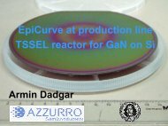
CPFC<br />
<strong>6x2</strong> [7x2] T/S MOCVD reactor<br />
�Mainly 3x3 and 1x4 c<strong>on</strong>figurati<strong>on</strong><br />
�For InP and GaAs based alloys<br />
�Quartz diffuser plate<br />
�Exhaust pipe-line “Widget”<br />
�<str<strong>on</strong>g>Laytec</str<strong>on</strong>g> ‘in-situ’ m<strong>on</strong>itoring<br />
�Pyrometry @ 950nm<br />
�reflectance @ 633nm [GaAs] and 950nm [InP]<br />
A.J.SpringThorpe – <str<strong>on</strong>g>Laytec</str<strong>on</strong>g> seminar - Metz – June 2008<br />
2
InP-based materials<br />
�1.3 and 1.55μm lasers<br />
� FP, DFB and BH<br />
�InGaAsP, InGaAs and InAlGaAs<br />
�P-i-N <str<strong>on</strong>g>detector</str<strong>on</strong>g>s - InGaAs<br />
�APD’s, QWIP’s<br />
�HBT’s<br />
�Quantum Dots<br />
A.J.SpringThorpe – <str<strong>on</strong>g>Laytec</str<strong>on</strong>g> seminar - Metz – June 2008<br />
3
GaAs, GaInAs, GaInP and AlGaAs<br />
�980nm lasers<br />
�Waveguides<br />
�Bragg reflectors<br />
�Multi-juncti<strong>on</strong> Solar Cells<br />
�QWIP’s - QCL’s<br />
�Quantum Dots<br />
�2DEG’s<br />
A.J.SpringThorpe – <str<strong>on</strong>g>Laytec</str<strong>on</strong>g> seminar - Metz – June 2008<br />
4
Single <str<strong>on</strong>g>Laytec</str<strong>on</strong>g> reflectance <str<strong>on</strong>g>head</str<strong>on</strong>g><br />
A.J.SpringThorpe – <str<strong>on</strong>g>Laytec</str<strong>on</strong>g> seminar - Metz – June 2008<br />
5
<str<strong>on</strong>g>Laytec</str<strong>on</strong>g> optical m<strong>on</strong>itoring <str<strong>on</strong>g>head</str<strong>on</strong>g> placement <strong>on</strong> the MOCVD reactor<br />
A.J.SpringThorpe – <str<strong>on</strong>g>Laytec</str<strong>on</strong>g> seminar - Metz – June 2008<br />
6
<str<strong>on</strong>g>Laytec</str<strong>on</strong>g> <str<strong>on</strong>g>detector</str<strong>on</strong>g> <str<strong>on</strong>g>head</str<strong>on</strong>g> layout<br />
DTT 1: 633 nm<br />
950 ± 70 nm DTT 2: 633 nm<br />
950 ± 70 nm<br />
950 ± 10 nm<br />
DTT 3: 950 ±<br />
70 nm<br />
A<br />
B<br />
C<br />
D<br />
D Ξ<br />
A.J.SpringThorpe – <str<strong>on</strong>g>Laytec</str<strong>on</strong>g> seminar - Metz – June 2008<br />
B<br />
C sees the susceptor<br />
7
GaAs and AlAs calibrati<strong>on</strong><br />
Mirror<br />
White light<br />
AsH 3<br />
Detectors<br />
@633nm<br />
@950nm<br />
GaAs substrate<br />
TMG<br />
TMA<br />
TMA-1 TMG-1 TMA-2 TMG-2<br />
A.J.SpringThorpe – <str<strong>on</strong>g>Laytec</str<strong>on</strong>g> seminar - Metz – June 2008<br />
8
InP growth rate calibrati<strong>on</strong> @ ~650 o C<br />
4.758Å/s<br />
4.625Å/s<br />
4.758Å/s<br />
+2.9%<br />
-1.8%<br />
Relative reflectance<br />
0.380<br />
0.360<br />
0.340<br />
0.320<br />
0.300<br />
0.280<br />
Relative reflectance @ 950nm<br />
Detector 1<br />
Detector 2<br />
Detector 3<br />
0.260<br />
1500 2000 2500 3000 3500 4000 4500<br />
time/s<br />
Special 3x3 susceptor to use all <str<strong>on</strong>g>three</str<strong>on</strong>g> <str<strong>on</strong>g>detector</str<strong>on</strong>g>s<br />
A.J.SpringThorpe – <str<strong>on</strong>g>Laytec</str<strong>on</strong>g> seminar - Metz – June 2008<br />
9
Reflectance at 950nm during n-InP epitaxy<br />
Substrate<br />
1.3E18 S-InP<br />
5E18 Si-InP<br />
5E17 Si-InP<br />
A.J.SpringThorpe – <str<strong>on</strong>g>Laytec</str<strong>on</strong>g> seminar - Metz – June 2008<br />
10
MOCVD Quantum dots<br />
�InAs<br />
�50%InGaAs<br />
�Need ‘in-situ’ m<strong>on</strong>itoring<br />
A.J.SpringThorpe – <str<strong>on</strong>g>Laytec</str<strong>on</strong>g> seminar - Metz – June 2008<br />
11
Formati<strong>on</strong> of InAs QDs – RHEED signature<br />
T=0s,<br />
0ML InAs<br />
GaAs c(4x4)<br />
T=1s,<br />
0.08ML InAs<br />
T=QD-0.5s,<br />
T=QD 0.5s,<br />
1.86ML InAs<br />
T=QD+0.5s,<br />
1.94ML InAs<br />
T=QD+2.0s,<br />
2.06ML InAs<br />
T=QD+4s,<br />
2.21ML InAs<br />
With thanks to Dr.Z. Wasilewski of NRC/IMS Epitaxy<br />
A.J.SpringThorpe – <str<strong>on</strong>g>Laytec</str<strong>on</strong>g> seminar - Metz – June 2008<br />
12
A.J.SpringThorpe – <str<strong>on</strong>g>Laytec</str<strong>on</strong>g> seminar - Metz – June 2008<br />
13
TMI bubbler c<strong>on</strong>figurati<strong>on</strong><br />
Carrier<br />
gas in<br />
0-1000 sccm<br />
Pusher<br />
Massflow c<strong>on</strong>trollers<br />
Flow in<br />
0-1000 sccm<br />
Minimum flow ~50 sccm<br />
Ξ ~0.1mL/s<br />
x<br />
x x<br />
To exhaust<br />
Pressure<br />
c<strong>on</strong>troller<br />
C<strong>on</strong>trol<br />
valves<br />
Organometallic<br />
Bubbler<br />
To<br />
reactor<br />
A.J.SpringThorpe – <str<strong>on</strong>g>Laytec</str<strong>on</strong>g> seminar - Metz – June 2008<br />
14
Minimum InAs growth rate calibrati<strong>on</strong><br />
RADS:-<br />
5x 15sec TMI @ ~50sccm<br />
200sec TEG @ 190sccm<br />
T g ~ 500 o C<br />
GaAs – 353.9 Å – 1.77Å/s<br />
InAs – 3.81Å - ~0.254Å/s - ~0.083mL/s<br />
22sec ~ 1.84mL<br />
A.J.SpringThorpe – <str<strong>on</strong>g>Laytec</str<strong>on</strong>g> seminar - Metz – June 2008<br />
15
Estimati<strong>on</strong> of InAs critical depositi<strong>on</strong> thickness<br />
Relative reflectance<br />
1.014<br />
1.012<br />
1.010<br />
1.008<br />
1.006<br />
1.004<br />
1.002<br />
1.000<br />
SI-GaAs - 0deg<br />
SI-GaAs - 2deg<br />
Critical<br />
depositi<strong>on</strong><br />
thickness<br />
~2+-0.22mL<br />
0 50 100 150 200 250 300<br />
Growth time [sec<strong>on</strong>ds]<br />
A.J.SpringThorpe – <str<strong>on</strong>g>Laytec</str<strong>on</strong>g> seminar - Metz – June 2008<br />
16
Estimati<strong>on</strong> of 50%InGaAs critical depositi<strong>on</strong> thickness<br />
5.0 5.2 5.4 5.6 5.8 6.0 6.2 6.4 6.6 6.8 7.0 mL<br />
Relaxati<strong>on</strong> starts after ~5.8mL<br />
A.J.SpringThorpe – <str<strong>on</strong>g>Laytec</str<strong>on</strong>g> seminar - Metz – June 2008<br />
17
Comparis<strong>on</strong> between 633nm and 950nm reflectance<br />
633nm 950nm<br />
5.0 5.2 5.4 5.6 5.8 6.0 6.2 6.4 6.6 6.8 7.0 mL 5.0 5.2 5.4 5.6 5.8 6.0 6.2 6.4 6.6 6.8 7.0 mL<br />
δR~1.2% δR~0.8%<br />
Reflectance changes are ~50% larger at 633nm as compared to 950nm<br />
A.J.SpringThorpe – <str<strong>on</strong>g>Laytec</str<strong>on</strong>g> seminar - Metz – June 2008<br />
18
Surface dot growth test –<br />
Structure<br />
22 sec InAs<br />
Reflectance at 633nm<br />
Cooldown<br />
AFM scan<br />
A.J.SpringThorpe – <str<strong>on</strong>g>Laytec</str<strong>on</strong>g> seminar - Metz – June 2008<br />
19
Buried dot growth test –<br />
Structure<br />
Photoluminesce<br />
532nm – 11mW<br />
22 sec InAs<br />
Reflectance at 633nm<br />
GaAs<br />
Surfscan<br />
10μm defects<br />
Plan View TEM<br />
500nm<br />
A.J.SpringThorpe – <str<strong>on</strong>g>Laytec</str<strong>on</strong>g> seminar - Metz – June 2008<br />
20
Structure<br />
Indium-Flush to improve surface morphology - 2<br />
25 sec InAs ~2mL<br />
10nm GaAs<br />
Ramp to 620C<br />
25nm GaAs<br />
60 sec anneal<br />
Surfscan<br />
Reflectance at 633nm<br />
10nm GaAs<br />
25nm GaAs<br />
Plan View TEM<br />
500nm<br />
~1.5E9 dots/cm 2<br />
~22nm in size<br />
A.J.SpringThorpe – <str<strong>on</strong>g>Laytec</str<strong>on</strong>g> seminar - Metz – June 2008<br />
21
Reflectance @ 633nm<br />
1.025<br />
1.020<br />
1.015<br />
1.010<br />
1.005<br />
1.000<br />
0.995<br />
0.990<br />
M1163 Reflectance @ 633nm<br />
Temperature (C)<br />
Reflectance @ 633nm<br />
640<br />
620<br />
600<br />
580<br />
560<br />
540<br />
0.985<br />
520<br />
0 50 100 150 200 250 300<br />
Time (sec<strong>on</strong>ds)<br />
500nm<br />
2.5mL InAs<br />
Increased InAs depositi<strong>on</strong><br />
Temperature ( o C)<br />
InAs ~2.5 and 3.0mL<br />
10nm GaAs<br />
Ramp to 620C<br />
25nm GaAs<br />
60 sec anneal<br />
1.025<br />
1.020<br />
1.015<br />
1.010<br />
1.005<br />
1.000<br />
0.995<br />
0.990<br />
~1.8E10/cm 2 ~3.2E10/cm 2<br />
Reflectance @ 633nm<br />
3.0mL InAs<br />
M1162 Reflectance @ 633nm<br />
Reflectance @ 633nm<br />
0.985<br />
520<br />
0 50 100 150 200 250 300<br />
Time (sec<strong>on</strong>ds)<br />
Temperature(oC)<br />
500nm<br />
A.J.SpringThorpe – <str<strong>on</strong>g>Laytec</str<strong>on</strong>g> seminar - Metz – June 2008<br />
640<br />
620<br />
600<br />
580<br />
560<br />
540<br />
22<br />
Temperature ( o C)
50% InGaAs surface QD’s <strong>on</strong> vicinal substrates – AFM 1μm square<br />
0-deg - 6.6E10/cm2 2-deg – 8.4E10/cm2 5-deg – 9.6E10/cm2 10-deg – 1E11/cm2<br />
1075<br />
0.00 2.00 4.00 6.00 8.00 10.00<br />
A.J.SpringThorpe – <str<strong>on</strong>g>Laytec</str<strong>on</strong>g> seminar - Metz – June 2008<br />
PL wavelength [nm]<br />
1275<br />
1250<br />
1225<br />
1200<br />
1175<br />
1150<br />
1125<br />
1100<br />
10 deg<br />
Arsine [sccm]<br />
0 Deg<br />
2 Deg<br />
5 Deg<br />
23
C<strong>on</strong>clusi<strong>on</strong>s:-<br />
�The <str<strong>on</strong>g>three</str<strong>on</strong>g> <str<strong>on</strong>g>head</str<strong>on</strong>g> reflectance unit enables precise growth rate<br />
and temperature uniformity measurements<br />
�Simple reflectance measurements can be used to<br />
m<strong>on</strong>itor the <strong>on</strong>set of relaxati<strong>on</strong> in quantum dot depositi<strong>on</strong><br />
�Shorter wavelengths are better – ~1.3% δR @ 633nm<br />
A.J.SpringThorpe – <str<strong>on</strong>g>Laytec</str<strong>on</strong>g> seminar - Metz – June 2008<br />
24
Acknowledgements:-<br />
�For TEM analysis<br />
Dr. Xiaohua Wu – NRC/IMS*<br />
Mr.Guy Parent – NRC/IMS<br />
�For AFM analysis<br />
Ms.Sim<strong>on</strong>a Moisa – NRC/IMS<br />
�For financial support<br />
Canadian Phot<strong>on</strong>ics Fabricati<strong>on</strong> Centre<br />
CMC Micro<str<strong>on</strong>g>system</str<strong>on</strong>g>s<br />
*Nati<strong>on</strong>al Research Council of Canada/Institute for Microstructural Sciences<br />
A.J.SpringThorpe – <str<strong>on</strong>g>Laytec</str<strong>on</strong>g> seminar - Metz – June 2008<br />
25